JP2005294940A - Semiconductor circuit device and operational amplifier - Google Patents
Semiconductor circuit device and operational amplifier Download PDFInfo
- Publication number
- JP2005294940A JP2005294940A JP2004103290A JP2004103290A JP2005294940A JP 2005294940 A JP2005294940 A JP 2005294940A JP 2004103290 A JP2004103290 A JP 2004103290A JP 2004103290 A JP2004103290 A JP 2004103290A JP 2005294940 A JP2005294940 A JP 2005294940A
- Authority
- JP
- Japan
- Prior art keywords
- circuit
- current
- transistor
- offset
- operational amplifier
- Prior art date
- Legal status (The legal status is an assumption and is not a legal conclusion. Google has not performed a legal analysis and makes no representation as to the accuracy of the status listed.)
- Pending
Links
- 239000004065 semiconductor Substances 0.000 title claims abstract description 30
- 238000010586 diagram Methods 0.000 description 16
- 238000012544 monitoring process Methods 0.000 description 6
- 238000000034 method Methods 0.000 description 5
- 230000003287 optical effect Effects 0.000 description 5
- 230000007423 decrease Effects 0.000 description 4
- 230000003321 amplification Effects 0.000 description 2
- 230000001419 dependent effect Effects 0.000 description 2
- 238000001514 detection method Methods 0.000 description 2
- 230000000694 effects Effects 0.000 description 2
- 238000003199 nucleic acid amplification method Methods 0.000 description 2
- 239000003990 capacitor Substances 0.000 description 1
- 230000005669 field effect Effects 0.000 description 1
- 238000004519 manufacturing process Methods 0.000 description 1
- 229910044991 metal oxide Inorganic materials 0.000 description 1
- 150000004706 metal oxides Chemical class 0.000 description 1
- 238000012986 modification Methods 0.000 description 1
- 230000004048 modification Effects 0.000 description 1
- 230000008929 regeneration Effects 0.000 description 1
- 238000011069 regeneration method Methods 0.000 description 1
Images


Landscapes
- Amplifiers (AREA)
Abstract
Description
本発明は、例えば光学式メディア用の記録再生装置の1つとして使用される光ピックアップに搭載される光ピックアップ用受光素子(Photo Detect Integrated Circuit:PDIC)などに使用される演算増幅器のオフセットを補償することができる半導体回路装置に関する。 The present invention compensates for an offset of an operational amplifier used in a light receiving element (Photo Detect Integrated Circuit: PDIC) mounted on an optical pickup used as one of recording / reproducing devices for optical media, for example. The present invention relates to a semiconductor circuit device that can be used.
従来、光ピックアップに搭載されるPDICの電圧出力値、及びその和・差の結果は、光学式メディアのトラック追従(トラッキング)、及び光学式メディアとの距離(フォーカス)制御信号として使用されている。 Conventionally, the voltage output value of a PDIC mounted on an optical pickup and the result of the sum / difference are used as a track follow-up (tracking) of an optical medium and a distance (focus) control signal with the optical medium. .
通常、PDICは1チップICと1つ以上の出力端子と1つ以上の電源端子とから構成され、このPDICには1つ以上のフォトダイオードとフォトダイオードに接続された1つ以上のオペアンプとが内蔵され、オペアンプの出力は出力端子に接続される。 Usually, a PDIC is composed of a one-chip IC, one or more output terminals, and one or more power supply terminals. The PDIC includes one or more photodiodes and one or more operational amplifiers connected to the photodiodes. The output of the operational amplifier is connected to the output terminal.
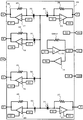
図7は、代表的な再生用PDICを示すブロック図である。通常、PDIC229は、複数のフォトダイオード230〜235と、このフォトダイオード230〜235に接続されたオペアンプ217〜222とを有し、これら各オペアンプ217〜222がそれぞれ各フォトダイオード230〜235に照射した光量に応じて発生する電流信号を電圧信号に変換増幅する。
FIG. 7 is a block diagram showing a typical playback PDIC. In general, the
すなわち、図7に示すように、PDIC229は、フォーカス信号用フォトダイオード230〜233と、このフォーカス信号用フォトダイオード230〜233とその反転入力端子とが接続されたそれぞれフォーカス信号用オペアンプ217〜220とを有する。各フォーカス信号用オペアンプ217〜220は、それぞれ負帰還回路223〜226を有し、その非反転入力端子は基準電位(Vc)251を供給する基準電源端子VCに接続され、それぞれ入力オフセット電圧を0に調整するためのオフセット電圧調整用入力257〜260を入力する図示せぬ端子を有する。そして、各フォーカス信号用アペアンプ217〜220の出力はフォーカス信号用出力端子A〜Dを介して出力される。以下、フォーカス信号用出力端子A〜Dを介して出力されるオペアンプ217〜220の出力をA〜D出力という。
That is, as shown in FIG. 7, the
また、PDIC229には、トラッキング信号用フォトダイオード234、235と、このトラッキング信号用フォトダイオード234、235とその反転入力端子とが接続されたそれぞれトラッキング信号用オペアンプ221、222とを有する。各トラッキング信号用オペアンプ221、222は、それぞれ負帰還回路227、228を有し、その非反転入力端子は基準電位(Vc)251を供給する基準電源端子VCに接続され、それぞれ入力オフセット電圧を0に調整するためのオフセット電圧調整用入力261、262を入力する図示せぬ端子を有する。そして、各トラッキング信号用アペアンプ221、222の出力は、トラッキング信号用出力端子E、Fを介して出力される。以下、トラッキング信号用出力端子E、Fを介して出力されるオペアンプ221、222の出力をE、F出力という。
The
PDIC229には、その他、IC内部で接続していないNon-connection端子NC、電源電位(Vcc)253を供給するための電源端子VCC、基準電源電位(Vc)251を供給するための基準電源端子VC、GND電位254を供給するためのGND端子GNDなどを備える。
The
このようなPDIC229においては、内蔵された各オペアンプ217〜222は各フォトダイオード230〜235に照射された光量に応じて発生する電流信号を電圧信号に変換増幅している。これがPDIC229のA〜E出力となる。ここで、PDIC229内のオペアンプ217〜222がオフセット電圧を有すると、PDIC229の出力が誤差を持つことになり、フォーカス制御やトラッキング制御が不完全で、正しくデータを読み出せないという不具合が発生してしまう。またオフセット電圧が温度変化、電源電圧変動に対して敏感であると同様の不具合の原因となりうる。
In such a
また、最近のPDICに求められる技術動向として、広帯域化、ゲイン切り替え機能化が挙げられる。これらの機能実現のためには、オペアンプの多段化が必須技術としてあげられるが、多段化とオフセット電圧のばらつきとにはトレードオフの関係がある。 Further, recent technical trends required for PDIC include wideband and gain switching function. In order to realize these functions, multi-stage operation of an operational amplifier is an essential technology, but there is a trade-off relationship between multi-stage operation and variations in offset voltage.
以上のことからも、特に影響が大きい初段のオペアンプにおける素子のばらつきによるオフセットの低減を図る必要がある。オペアンプのオフセット電圧を低減するための方法として、オペアンプ内の差動増幅器に対してオフセット補償回路を設ける方法がある(例えば特許文献1など)。 From the above, it is necessary to reduce the offset due to device variations in the first-stage operational amplifier, which has a particularly large influence. As a method for reducing the offset voltage of the operational amplifier, there is a method of providing an offset compensation circuit for the differential amplifier in the operational amplifier (for example, Patent Document 1).
図8は、従来の差動回路を示す回路図である。図8に示すように、従来の差動回路は、非反転入力端子にベースが接続されるNPNトランジスタ203及び反転入力端子にベースが接続されるNPNトランジスタ204からなる差動対トランジスタと、トランジスタ203のコレクタにコレクタが接続されベースとコレクタとが短絡されたPNPトランジスタ201及びこのトランジスタ201のベースにベースが接続されたPNPトランジスタからなるアクティブ・ロードと、一端がトランジスタ201及び202のエミッタにそれぞれ接続され、他端が電源電位(Vcc)253に接続されたそれぞれ抵抗209、210と、バイアス電流源207とにより差動アンプ部DAが構成される。また、ドライブトランジスタ206と、このトランジスタ206のベース電流をモニタするモニタトランジスタ205と、ドライブ電流源208とからドライバ部DVが構成される。ここで、バイアス電流源207、208は、通常カレント・ミラー回路から構成される。
FIG. 8 is a circuit diagram showing a conventional differential circuit. As shown in FIG. 8, the conventional differential circuit includes a differential transistor composed of an
トランジスタ205は、トランジスタ206とカスケード接続して、トランジスタ206のベース電流をモニタする。トランジスタ205のベース電流を、アクティブ・ロードを構成するカレント・ミラー回路のトランジスタ201のエミッタ側へ帰還すると、トランジスタ201のエミッタ電位はトランジスタ205のベース電流×抵抗209の抵抗Rの電位分だけ下がる。この電位分はトランジスタ202及び抵抗210によって電流に変換され、抵抗209及び抵抗210の抵抗値を同一としたときトランジスタ202のコレクタにはトランジスタ205のベース電流の分だけ多く電流が流れる。トランジスタ205、206 はカスコード接続してそれらのベース電流をほぼ等しくしていることから、トランジスタ206のベースにはトランジスタ202のコレクタ電流の増加分、すなわち、トランジスタ205のベース電流のみ流れ込む。これより、トランジスタ204に流れ込む電流はトランジスタ206のベース電流の影響を受けることなく、オフセット補償を施すことができる。
すなわち、従来の差動回路においては、非反転入力端子及び反転入力端子から入力されたそれぞれ+端子入力251及び−端子入力252よりなる差動入力は、NPNトランジスタ203及び204の差動対を介して増幅され、その出力はNPNトランジスタ204のコレクタより取出され、更に、NPNトランジスタ206によるエミッタフォロアを介して、出力端子から出力255として出力される。NPNトランジスタ206のベース電流により、NPNトランジスタ203、204のコレクタ電流に差異が生じ、ベース・エミッタ電圧に差が生じて入力に対するオフセット電圧を生ずるが、このオフセット電圧が、NPNトランジスタ205を付加することにより補償される。すなわち、このトランジスタ205がオフセット補償回路を構成する。
しかしながら、この従来の差動回路においては、PNPトランジスタ201、202のベース電流によるトランジスタ203のコレクタ電流増分はPNPトランジスタ201、202の直流電流増幅率hFEに依存し、トランジスタ205、206のベース電流は205、206及び208のNPNトランジスタのhFEに依存している。通常PNPのhFEとNPNのhFEの間に相関はないため、このような固定電流源ではオフセット電圧のばらつきを完全に補償できない場合がある。
However, this conventional differential circuit, the collector current increment of the
また、電源電圧変動、温度変動特性に関しても同様に、PNPトランジスタのアーリ電圧とNPNトランジスタのアーリ電圧に相関はない。更に、抵抗についてもNPNトランジスタ、PNPトランジスタの品質及び素子特性に相関がない。以上のことから、上述の従来の差動回路においては、オフセット電圧のばらつきを完全に補償することができないという問題点がある。 Similarly, regarding the power supply voltage fluctuation and temperature fluctuation characteristics, there is no correlation between the Early voltage of the PNP transistor and the Early voltage of the NPN transistor. Further, the resistance has no correlation with the quality and element characteristics of the NPN transistor and the PNP transistor. From the above, the conventional differential circuit described above has a problem in that it is not possible to completely compensate for variations in offset voltage.
本発明は、このような問題点を解決するためになされたものであり、品質及び素子特性が異なるトランジスタを使用した演算増幅器であってもそのオフセットを補償することができる半導体回路装置を提供することを目的とする。 The present invention has been made to solve such problems, and provides a semiconductor circuit device capable of compensating for an offset even in an operational amplifier using transistors having different quality and element characteristics. For the purpose.
本発明にかかる半導体回路装置は、基準電位と比較電位との差に基づき出力信号を出力する演算増幅器の該出力信号に対応したモニタ電位と、基準電位とを比較する比較回路と、前記比較回路の比較結果に基づき前記演算増幅器のオフセットを補償するように当該演算増幅器に含まれる差動増幅回路の動作電流を調整する電流調整回路とを有することを特徴とする。 A semiconductor circuit device according to the present invention includes a comparison circuit that compares a reference potential with a monitor potential corresponding to the output signal of an operational amplifier that outputs an output signal based on a difference between the reference potential and the comparison potential, and the comparison circuit. And a current adjusting circuit that adjusts the operating current of the differential amplifier circuit included in the operational amplifier so as to compensate for the offset of the operational amplifier based on the comparison result.
本発明においては、モニタ電位と基準電位とを比較した比較結果に基づき演算増幅器に含まれる差動増幅回路の動作電流を調整するため、差動増幅回路に含まれる素子のバラツキなどによって生じるオフセットを補償することができる。 In the present invention, since the operating current of the differential amplifier circuit included in the operational amplifier is adjusted based on the comparison result obtained by comparing the monitor potential with the reference potential, an offset caused by variations in elements included in the differential amplifier circuit is eliminated. Can be compensated.
この場合、前記電流調整回路は、例えば、前記差動増幅回路に含まれる差動対のテール電流に流れる電流量を調整することができ、差動増幅回路の動作電流としてのテール電流の電流量を調整することでオフセットを補償することができる。 In this case, for example, the current adjustment circuit can adjust the amount of current flowing in the tail current of the differential pair included in the differential amplifier circuit, and the amount of tail current as the operating current of the differential amplifier circuit The offset can be compensated by adjusting.
また、前記電流調整回路は、例えば、前記電流調整回路は、前記差動増幅回路に含まれる差動対の負荷側に流れる負荷電流の電流量を調整することができ、この場合、前記差動対の基準電位が入力される側の負荷電流、又は前記差動対の負荷として設けられたカレント・ミラー回路と前記差動対との間のノードに流れる負荷電流の電流量を調整してもよく、差動増幅回路の動作電流としての負荷電流の電流量を調整することでオフセットを補償してもよい。 Further, the current adjustment circuit can adjust, for example, the amount of load current flowing to the load side of the differential pair included in the differential amplifier circuit. Even if the load current on the side to which the reference potential of the pair is input or the amount of load current flowing to the node between the differential pair and the current mirror circuit provided as the load of the differential pair is adjusted The offset may be compensated by adjusting the amount of load current as the operating current of the differential amplifier circuit.
ここで、前記モニタ電位は、前記比較回路が比較する基準電位との差が、前記演算増幅器のオフセットと同一極性とすることができ、モニタ電位は、演算増幅回路のオフセットが正のオフセットである場合には、基準電位より大きく、オフセットが負のオフセットである場合は、基準電位より小さい電位とされる。 Here, the monitor potential can have the same polarity as the offset of the operational amplifier so that the difference between the monitor potential and the reference potential to be compared is the same as the offset of the operational amplifier. In this case, if the offset is larger than the reference potential and the offset is a negative offset, the potential is smaller than the reference potential.
また、前記比較回路は、一方のトランジスタの制御端子が前記基準電位に接続され他方のトランジスタの制御端子が前記モニタ電位に接続される差動対と、前記差動対に接続された定電流源とを有することができ、比較回路は、差動回路として構成することができる。 The comparison circuit includes a differential pair in which a control terminal of one transistor is connected to the reference potential and a control terminal of the other transistor is connected to the monitor potential, and a constant current source connected to the differential pair The comparison circuit can be configured as a differential circuit.
更に、前記電流調整回路は、前記電流調整回路は、ダイオード接続されたトランジスタと、当該トランジスタと前記比較回路の出力に応じて電流量が変化するカレント・ミラー回路を構成する調整電流出力用トランジスタとを有することができ、調整電流用トランジスタにモニタ電位に応じて自動調整可能な調整電流を流す電流源を構成することができる。 Further, the current adjustment circuit includes a diode-connected transistor, and an adjustment current output transistor constituting a current mirror circuit in which an amount of current changes according to an output of the transistor and the comparison circuit. The current source can be configured to flow an adjustment current that can be automatically adjusted according to the monitor potential to the adjustment current transistor.
更にまた、前記電流調整回路は、前記ダイオード接続されたトランジスタと前記カレント・ミラー回路を構成する複数の前記調整電流出力用トランジスタを有し、各調整電流出力用トランジスタは、複数の演算増幅器のオフセットを個別に補償するようにそれぞれ複数の演算増幅器に含まれる差動増幅回路の動作電流を調整してもよく、調整電流出力用トランジスタを複数設けることで、複数の演算増幅器を個別に補償することができる。 Furthermore, the current adjustment circuit includes the diode-connected transistor and a plurality of adjustment current output transistors constituting the current mirror circuit, and each adjustment current output transistor includes offsets of a plurality of operational amplifiers. The operational currents of the differential amplifier circuits included in each of the plurality of operational amplifiers may be adjusted so that each of the operational amplifiers is individually compensated, and the plurality of operational amplifiers are individually compensated by providing a plurality of adjustment current output transistors. Can do.
更にまた、前記モニタ電位を出力するオフセットモニタ回路を有し、前記比較回路は、前記基準電位と前記モニタ回路の出力とを比較することができ、モニタ回路を内蔵した半導体回路装置とすることができる。 Furthermore, an offset monitor circuit for outputting the monitor potential is provided, and the comparison circuit can compare the reference potential with the output of the monitor circuit, and a semiconductor circuit device incorporating the monitor circuit is provided. it can.
また、前記オフセットモニタ回路は、前記演算増幅器の前記差動増幅回路に含まれる差動対及び該差動対の負荷として設けられるカレント・ミラー回路と同一導電性のトランジスタを有する差動増幅回路を有することができ、更に、前記演算増幅器に含まれる前記差動増幅回路の出力と当該演算増幅器の出力との間に設けられる帰還回路に対応する帰還回路を有することができ、演算増幅器と同一導電性のトランジスタ、帰還回路を有するものとすれば、演算増幅器と同様のオフセットを正確に生じさせることができる。 The offset monitor circuit includes a differential amplifier circuit including a differential pair included in the differential amplifier circuit of the operational amplifier and a transistor having the same conductivity as a current mirror circuit provided as a load of the differential pair. And a feedback circuit corresponding to a feedback circuit provided between the output of the differential amplifier circuit included in the operational amplifier and the output of the operational amplifier. If it has a transistor and a feedback circuit, the same offset as that of the operational amplifier can be generated accurately.
また、前記演算増幅器を有し、前記演算増幅器は、一方のトランジスタの制御端子に基準電位が接続され他方のトランジスタの制御端子に比較電位が接続される差動対と、前記差動対に負荷として接続されるカレント・ミラー回路と、前記差動対に接続された定電流源と、前記差動対と前記カレント・ミラー回路との間のノードに制御端子が接続されたオフセット補償用トランジスタとを有し、前記調整電流出力用トランジスタは、前記オフセット補償用トランジスタと直列に接続されることができ、上述したオフセット補償回路としての半導体回路装置を演算増幅器と共に搭載した半導体回路装置を提供することができ、この場合、調整電流出力用トランジスタはカレント・ミラー回路と差動対との間のノードに接続されたオフセット補償用トランジスタと直列に接続されることで、調整電流出力用トランジスタが出力する調整電流をオフセット補償用トランジスタに流すことで演算増幅器のカレント・ミラー回路に流れる負荷電流を調整してオフセットを吸収することができる。 The operational amplifier has a differential pair in which a reference potential is connected to a control terminal of one transistor and a comparison potential is connected to a control terminal of the other transistor, and a load is applied to the differential pair. A current mirror circuit connected as a constant current source connected to the differential pair, an offset compensation transistor having a control terminal connected to a node between the differential pair and the current mirror circuit; The adjustment current output transistor can be connected in series with the offset compensation transistor, and a semiconductor circuit device in which the semiconductor circuit device as the offset compensation circuit described above is mounted together with an operational amplifier is provided. In this case, the adjustment current output transistor is offset compensated for the node between the current mirror circuit and the differential pair. By connecting in series with the transistor, the adjustment current output from the adjustment current output transistor can be passed through the offset compensation transistor to adjust the load current flowing in the current mirror circuit of the operational amplifier to absorb the offset. it can.
また、前記演算増幅器を有し、前記演算増幅器は、前記演算増幅器は、一方のトランジスタの制御端子に基準電位が接続され他方のトランジスタの制御端子に比較電位が接続される差動対と、前記差動対に負荷として接続されたカレント・ミラー回路とを有し、前記調整電流出力用トランジスタは、前記差動対に接続され、該調整電流出力用トランジスタを出力する調整電流をテール電流とすることができ、調整電流をテール電流とすることで差動対に流れる電流を調整してオフセットを吸収することができる。 The operational amplifier includes a differential pair in which a reference potential is connected to a control terminal of one transistor and a comparison potential is connected to a control terminal of the other transistor; A current mirror circuit connected as a load to the differential pair, and the adjustment current output transistor is connected to the differential pair, and the adjustment current output from the adjustment current output transistor is a tail current. The offset current can be absorbed by adjusting the current flowing in the differential pair by using the tail current as the adjustment current.
更に、受光量に応じた電圧を前記比較電位として出力するフォトダイオードを有することができ、フォトダイオードの検出出力を比較電位として出力する演算増幅器及びそのオフセットを補償する受光検出回路としての半導体回路装置を提供することができる。 Furthermore, it can have a photodiode that outputs a voltage corresponding to the amount of received light as the comparison potential, an operational amplifier that outputs the detection output of the photodiode as a comparison potential, and a semiconductor circuit device as a light reception detection circuit that compensates for the offset Can be provided.
本発明に係る半導体回路装置によれば、品質及び素子特性が異なるトランジスタを使用した演算増幅器のオフセットを補償することができる。 According to the semiconductor circuit device of the present invention, it is possible to compensate for an offset of an operational amplifier using transistors having different quality and element characteristics.
以下、本発明を適用した具体的な実施の形態について、図面を参照しながら詳細に説明する。この実施の形態は、本発明を、演算増幅器と、演算増幅器に含まれるNPNトランジスタ、PNPトランジスタ、及び抵抗などの素子特性の影響を演算増幅器と同様に受け、同様のオフセットを生じるようなオフセットモニタ回路と、このオフセットモニタ回路を使用して上記演算増幅器のオフセットを間接的にモニタし、このモニタ結果に基づき演算増幅回路のオフセットを自動調整することができるオフセット補償回路用電流源としてのオフセット補償回路とを有する半導体回路装置に適用したものである。 Hereinafter, specific embodiments to which the present invention is applied will be described in detail with reference to the drawings. This embodiment is an offset monitor in which the present invention is affected by the operational amplifier and the element characteristics such as the NPN transistor, the PNP transistor, and the resistance included in the operational amplifier in the same manner as the operational amplifier, and generates the same offset. Offset compensation as a current source for an offset compensation circuit capable of indirectly monitoring the offset of the operational amplifier using the circuit and the offset monitor circuit and automatically adjusting the offset of the operational amplifier circuit based on the monitoring result The present invention is applied to a semiconductor circuit device having a circuit.
発明の実施の形態1.
先ず、本発明の実施の形態1について説明する。演算増幅器、オフセットモニタ回路及びオフセット補償回路を搭載した半導体回路装置の一例としてPDICがある。PDICは1チップICと1つ以上の出力端子と1つ以上の電源端子とから構成され、ICには1つ以上のフォトダイオードとフォトダイオードに接続された1つ以上のオペアンプとが内蔵され、オペアンプの出力は出力PINに接続されている。本実施の形態は、PDICなどに含まれる演算増幅器(以下、オペアンプという。)のオフセット電圧を補償するためのオフセット電圧補償回路をオペアンプと共に搭載した回路装置である。なお、以下の実施の形態においては、半導体回路装置をPDICとして説明するが、本実施の形態におけるオフセット補償回路が補償するオフセットは、PDICに搭載されるオペアンプに限らず、他の用途のオペアンプを有する回路であってもよい。
First,
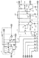
図1は、本発明の実施の形態1にかかるオフセット補償回路を搭載した半導体回路装置の一例であるPDICを示すブロック図である。PDIC29は、複数のフォトダイオード30〜35と、このフォトダイオード30〜35に接続された複数のオペアンプ17〜22とを有し、これら各オペアンプ17〜22がそれぞれ各フォトダイオード30〜35に照射した光量に応じて発生する電流信号を電圧信号に変換増幅する。
FIG. 1 is a block diagram showing a PDIC which is an example of a semiconductor circuit device equipped with an offset compensation circuit according to the first embodiment of the present invention. The
すなわち、図1に示すように、PDIC29は、フォーカス信号用フォトダイオード30〜33と、このフォーカス信号用フォトダイオード30〜33にその反転入力端子が接続されたそれぞれフォーカス信号用オペアンプ17〜20とを有する。各フォーカス信号用オペアンプ17〜20は、それぞれ負帰還回路23〜26を有し、その非反転入力端子は基準電位(Vc)51に接続され、それぞれ入力オフセット電圧を0に調整するためのオフセット電圧調整用入力57〜60を入力する図示せぬ端子が設けられる。そして、各フォーカス信号用アペアンプ17〜20の出力は、フォーカス信号用出力A〜Dが端子を介して出力される。以下、フォーカス信号用出力端子A〜Dを介して出力されるオペアンプ17〜22の出力をA〜D出力という。
That is, as shown in FIG. 1, the
また、PDIC29には、トラッキング信号用フォトダイオード34、35と、このトラッキング信号用フォトダイオード34、35にその反転入力端子が接続されたそれぞれトラッキング信号用オペアンプ21、22とを有する。各トラッキング信号用オペアンプ21、22は、それぞれ負帰還回路27、28を有し、その非反転入力端子は基準電位(Vc)51に接続され、それぞれ入力オフセット電圧を0に調整するためのオフセット電圧調整用入力61、62を入力する図示せぬ端子が設けられる。そして、各トラッキング信号用アペアンプ21、22の出力は、トラッキング信号用出力端子E、Fを介して出力される。以下、トラッキング信号用出力端子E、Fを介して出力されるオペアンプ221、222の出力をE、F出力という。
Further, the
そして、このPDIC29には更に、オフセット電圧調整用入力57である調整電流を出力するオフセット補償回路14と、これに接続されたオフセットモニタ用オペアンプであるオフセットモニタ回路15とを有する。オフセットモニタ回路15は、その非反転入力端子に基準電位(Vc)51が供給され、その出力と反転入力端子とに接続されたオフセットモニタ用帰還回路QM12を有する。そして、このオフセット補償回路14のトランジスタQN5のベース電流56が、カレント・ミラー回路を介してオフセット電圧調整用入力57〜62用の端子に入力されることで、フォーカス信号用、トラッキング信号用のオペアンプ17〜22のオフセットを調整する。
The
PDIC29には、その他、IC内部で接続していないNon-connection端子NC、電源電位(Vcc)53を供給するための電源端子VCC、基準電位(Vc)51を供給するための基準電源端子VC、GND電位54を供給するためのGND端子GNDなどを備える。
The
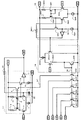
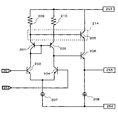
図2は、図1に示すPDIC29のうち、オフセット補償回路14及びオフセットモニタ回路15を示す回路図である。図2には、このオフセット補償回路14に接続されるフォーカス信号用オペアンプ17(以下、A出力オペアンプともいう。)も合わせて示す。オフセットモニタ回路15は、フォーカス信号、トラッキング信号用オペアンプと同じオペアンプ回路形式を取っており、例えばフォーカス信号用オペアンプ17のオフセットと同様のオフセットを生じるような回路となっている。オフセット補償回路14は、このオフセットモニタ回路15に生じるオフセットに基づき、図1に示したフォーカス信号用オペアンプ17〜20、トラッキング信号用オペアンプ21、22などのオフセットを補償するものである。
FIG. 2 is a circuit diagram showing the offset
例えばフォーカス信号用オペアンプであるA出力オペアンプ17は、基準電位(Vc)51にベースが接続されたNPNトランジスタ3、及びフォトダイオード30のカソードにベースが接続されたNPNトランジスタ4からなる差動対と、一端が電源電位(Vcc)53に接続された抵抗9、10と、トランジスタ3のコレクタにコレクタが接続され、エミッタに抵抗9の他端が接続されベースとコレクタとが短絡されたPNPトランジスタ1、及びエミッタに抵抗10の他端が接続され、ベースがトランジスタ1のベースと接続されコレクタがトランジスタ4のコレクタに接続されたNPNトランジスタ2からなり、前記差動対の負荷となるカレント・ミラー回路と、トランジスタ3、4のエミッタに接続されたテール電流を流す定電流源7と、トランジスタ4のコレクタにベースが接続されたエミッタフォロア回路(NPNトランジスタ)6と、トランジスタ6のエミッタに接続された出力バッファ回路11と、出力バッファ回路11の出力とトランジスタ4のベースとの間に設けられた、抵抗及びコンデンサを有する帰還回路23と、トランジスタ1のコレクタに制御端子であるベースが接続されたオフセット補償用トランジスタとしてのNPNトランジスタ5とを有する。このトランジスタ5のエミッタ電流を後述する調整電流とすることにより、A出力オペアンプ17のオフセットを補償することができる。
For example, the A output
このA出力オペアンプ17のオフセットは、このA出力オペアンプ17を構成する例えば、PNPトランジスタ1、2、NPNトランジスタ3、4、帰還回路23の素子バラツキなどによって生じ、A出力55が例えば基準電位(Vc)より大きくなったり、小さくなったりするものである。これを防止するためには、トランジスタ5に適当な電流を流してオフセットを吸収する必要があるが、オフセットによるA出力は、上記の素子特性によって一定とはならないため、オフセットに応じた調整電流を流してオフセットを吸収する必要がある。この調整電流を流すためのオフセット補償回路14は、基準電位(Vc)とA出力55に対応するモニタ電位とを比較する比較回路としての差動増幅器(差動回路)と、比較回路の比較結果に応じて、オフセットを補償するようにA出力オペアンプの差動増幅器の動作電流を調整する電流調整回路とを有している。
The offset of the A output
ここで、オフセットモニタ回路15は、オフセット補償回路14のトランジスタQN2のベースへの出力16を、オペアンプ17のA出力と同様のオフセットを生じさせるためのダミー回路として機能する。このため、本実施の形態におけるオフセットモニタ回路15は、オペアンプ17と、オフセット補償用トランジスタ5以外は同様の構成とする。これにより、オペアンプ17のオフセットを間接的にモニタすることができる。
Here, the offset
すなわち、本実施の形態におけるオフセットモニタ回路15は、差動対トランジスタを構成するPNPトランジスタQM3、QM4と、アクティブ・ロード(能動負荷)となるNPNトランジスタQM1、QM2と、抵抗QM8、QM9と、定電流源QM7とから差動アンプDAと、ドライブトランジスタQM5と、ドライブ電流源となる定電流源QM7とからドライバ部DVとを有している。
That is, the offset
このように、オフセットモニタ回路15を、A出力オペアンプ17と同様の構成とすることで、A出力オペアンプ17と同様のオフセットを生じさせるものである。ここで、A出力オペアンプと同じ大きさのオフセットを生じさせる回路として、本実施の形態におけるオフセットモニタ回路15は、少なくともA出力オペアンプ17と以下の構成を同様とするものとする。すなわち、A出力オペアンプ17の差動増幅器3、4に対応するトランジスタQM3、4、カレント・ミラー回路を構成するトランジスタ1、2に対応するトランジスタQM1、QM2、帰還回路23に対応するQM12である。また、この場合、オフセットモニタ回路15とオペアンプとにおいて、差動対、カレント・ミラー回路などを構成するトランジスタを同一導電性にし、同一プロセスで製造されたものとすれば、極めて高精度にオペアンプ17のオフセットをモニタできるものとなる。すなわち、オフセットモニタ回路15は、A出力オペアンプ17とほぼ同様のオフセットを生じさせることができる。
As described above, the offset
次に、オフセット補償回路14について説明する。オフセット補償回路14は、基準電位(Vc)とオフセットモニタ回路15の出力16とを比較する比較回路と、この比較結果に応じた調整電流を出力してオフセットの原因となっているオペアンプ17の差動増幅器に流れる動作電流を調整する電流調整回路とからなり、調整電流と同一の電流をA出力オペアンプ17のトランジスタ5に流すことにより、A出力オペアンプ17のオフセットを補償するものである。
Next, the offset
このため、オフセット補償回路14は、比較回路として、基準電位(Vc)にベースが接続されたNPNトランジスタQN1、及びモニタ電位を出力する出力16にベースが接続されたNPNトランジスタQN2からなる差動対と、これらトランジスタ対のエミッタに接続された定電流源QN12とからなるNPN型差動増幅器を有する。
For this reason, the offset
また、比較結果に応じて調整電流を出力する電流調整回路として、トランジスタQN1のコレクタの電流を増幅するためのPNPトランジスタQN3、QN4からなるPNP型カレント・ミラー回路と、このカレント・ミラー回路に接続されるダイオード接続されたNPNトランジスタ(エミッタ接地回路)5と、NPNトランジスタ5と共にNPN型カレント・ミラー回路を構成する調整電流出力用トランジスタとしてのNPNトランジスタQN6〜QN11とを有し、トランジスタQN6〜QN11に流れるコレクタ電流が調整電流となっている。
Further, as a current adjustment circuit that outputs an adjustment current according to the comparison result, a PNP type current mirror circuit composed of PNP transistors QN3 and QN4 for amplifying the collector current of the transistor QN1, and a connection to the current mirror circuit Diode-connected NPN transistor (grounded emitter circuit) 5 and NPN transistors QN6 to QN11 as adjusting current output transistors which form an NPN current mirror circuit together with the
ここで、トランジスタQN5のベース端子は、トランジスタQN1、QN2から構成される差動アンプの基準電圧側に接続され、トランジスタQN5のエミッタ端子はQN6、7、8、9、10、11のいずれか1以上のエミッタ端子と接続され、ベースとコレクタとが短絡されてダイオード接続されている。このトランジスタQN5とカレント・ミラー回路を構成するトランジスタQN6は、エミッタが接地され、ベースがトランジスタQN5と接続され、更にA出力オペアンプ17のトランジスタ5と直列に接続されている。すなわち、トランジスタQN6のコレクタ電流は、調整電流として、A出力オペアンプ17のトランジスタ5のコレクタ電流(57)となるよう構成されている。
Here, the base terminal of the transistor QN5 is connected to the reference voltage side of the differential amplifier composed of the transistors QN1 and QN2, and the emitter terminal of the transistor QN5 is any one of QN6, 7, 8, 9, 10, and 11. Connected to the above emitter terminal, the base and collector are short-circuited and diode-connected. The transistor QN5 and the transistor QN6 constituting the current mirror circuit have an emitter grounded, a base connected to the transistor QN5, and further connected in series with the
トランジスタQN1のコレクタ側に接続されるカレント・ミラー回路は、トランジスタQN1のコレクタにコレクタが接続されエミッタにトランジスタQN2のコレクタが接続され、ベースとコレクタとが短絡されたPNPトランジスタQN3と、トランジスタQN3とベース同士が接続されたPNPトランジスタQN4とから構成され、トランジスタQN4のコレクタと第3のトランジスタとしてのトランジスタQN5のコレクタとが接続される。 The current mirror circuit connected to the collector side of the transistor QN1 includes a PNP transistor QN3 in which the collector is connected to the collector of the transistor QN1, the collector of the transistor QN2 is connected to the emitter, and the base and collector are short-circuited; The base is connected to a PNP transistor QN4, and the collector of the transistor QN4 and the collector of the transistor QN5 as the third transistor are connected.
オフセットは、オペアンプ17を構成するNPNトランジスタ3,4、PNPトランジスタ1,2、及び帰還回路23などの素子特性のバラツキにより、差動増幅器に流れる電流(動作電流)のバランスがくずれて生じるものである。差動増幅器に流れる電流としては、トランジスタ1,2からなるカレント・ミラー回路に流れる電流、すなわち、トランジスタ3,4のコレクタ電流、トランジスタ3,4からなる差動対に流れる電流、すなわち、トランジスタ3,4のコレクタ電流、エミッタ電流、電流源7に流れるテール電流などである。
The offset is caused by the balance of the current (operating current) flowing through the differential amplifier due to variations in element characteristics such as the
本実施の形態においては、これらの電流のうち、カレント・ミラー回路を構成するトランジスタ3の差動対の入力側のトランジスタ1との間のノードに接続されたトランジスタ5のエミッタ電流を調整電流とすることでトランジスタ1のコレクタ電流の電流量を調整してオフセットを補償するものである。なお、後述するように、上記テール電流を調整してオフセットを補償するように構成することも可能である。
In this embodiment, among these currents, the emitter current of the
ここで、通常、1チップ内の複数のオペアンプ、すなわち、本実施の形態においては、オペアンプ17〜22、及びオフセットモニタ回路15のオペアンプは、同じオフセット電圧を出力し、電源電圧変動、温度変動特性も等しくなる。すなわち、このように構成されたA出力オペアンプ17、オフセットモニタ回路15及びオフセット補償回路14においては、例えば出力Aのオペアンプ17と、これと同様に構成されたオフセットモニタ回路15とは、同様の動作をすることで、オフセット補償回路14は、オフセットモニタ回路15のオフセットを補償するように動作することで、A出力オペアンプ17のオフセットを補償することができる。
Here, normally, a plurality of operational amplifiers in one chip, that is, in the present embodiment, the
次に、これらの回路の動作について説明する。ここでは、例えば、ロットバラツキなどによって、直流電流増幅率hFEが目的の値よりも低いPNPトランジスタが製造された場合の動作について説明する。すなわち、図2に示すA出力オペアンプ17において、PNPトランジスタ1、2のhFEが目的の値より小さい場合、PNPトランジスタ1、2のベース電流が増加する。PNPトランジスタ1は、ベースとコレクタとが短絡されているため、PNPトランジスタ1のベース電流が増加すればそのコレクタ電流も増加することとなる。これにより、トランジスタ3のベース−エミッタ間電圧がトランジスタ4のベース−エミッタ間電圧より大きくなる。これにより、トランジスタ4のベース電位が低下し、帰還回路23を介してA出力55は、基準電圧(Vc)51よりも低い電圧(負のオフセット電圧)を出力しようとする。
Next, the operation of these circuits will be described. Here, for example, by lot variations, the DC current amplification factor h FE will be described operation when the lower PNP transistor than the desired value is produced. That is, in the A output
このとき、同一チップ内にて同様の構成を有するオフセットモニタ回路15においても、A出力オペアンプ17と同様の現象が生じる。すなわち、同じくトランジスタQM1、2のhFEが小さいものとなっており、トランジスタQM4のベース電位が基準電位(Vc)より低くなってしまい、したがって帰還回路QM12を介した出力16の電位も基準電位(Vc)より低下して負のオフセットを生じる。これにより、オフセット補償回路14の入力に、オフセットモニタ回路15からの出力16が負のオフセット電圧として入力されることになる。
At this time, the same phenomenon as the A output
オフセット補償回路14に負のオフセット電圧が入力されるとトランジスタQN2のコレクタ電流が増加し、あわせてQN5のベース電流も増え、カレント・ミラー回路で増幅されたQN6〜QN11のコレクタ電流(57〜62)も増加することになる。この増幅された調整電流57は、トランジスタ5のエミッタ電流となる。これにより、トランジスタ5のベース電流が増加し、PNPトランジスタのhFEの低下によるトランジスタ2へのコレクタ電流の増加を防ぐことができる。こうして、A出力55は、ほぼ基準電圧(Vc)を出力するようになり、オフセットを吸収することができる。
When a negative offset voltage is input to the offset
同様にして、その他のオペアンプ18〜22も、トランジスタQN7〜QN11に流れる調整電流によりオフセットが吸収され、B〜F出力が基準電圧(Vc)を出力するようになり、オフセット電圧、オペアンプの和及び差の出力特性も改善することができる。また、電源電圧変動、温度変動に対しても同様のオフセット電圧低減効果を奏する。ここで、トランジスタQN3、QN4からなるカレント・ミラー回路のカレント・ミラー回路比を適宜設定して出力電流56を所望の値に調整することができ、また、トランジスタQN5〜QN11からなるカレント・ミラー回路のカレント・ミラー回路比を適宜設定することにより、出力電流(調整電流)57〜62の大きさを適宜設定することができ、1つのオフセット補償回路により、オフセット補償をするオペアンプ17〜22毎に個別に調整電流を設定することができる。なお、オペアンプ毎にオフセット補償回路を設けてもよく、オペアンプ毎に異なる構成である場合や異なる素子特性の素子を使用している場合などにおいては、オフセットモニタ回路を設けてもよい。
Similarly, in the other
なお、A出力オペアンプ17と同種の極性のオフセットを生じさせることができれば、オフセットモニタ回路15の構成はこれに限るものではなく、オフセットモニタ回路15は、少なくともA出力オペアンプ17の基準電位(Vc)に対するA出力の極性と同一となる出力16となるものであってもよい。この場合、本実施の形態におけるオフセット補償回路14の比較回路は、一方のトランジスタQN1のベースには基準電位(Vc)51が接続され、他方のトランジスタQN2のベースにはオフセットモニタ回路15の出力(モニタ電位)16に接続される差動対を有するものであるが、この差動対が少なくとも、オフセットによりA出力オペアンプ17のA出力が基準電位(Vc)より高いか低いかを比較できればよい。すなわち、トランジスタQN2に入力されるモニタ電位(出力16)は、トランジスタQN1に入力される基準電位との差が、オペアンプ17に入力される基準電位とそのA出力との差と同一極性となっていればよく、オペアンプ17のA出力が基準電位(Vc)51より高いときは、オフセット補償回路14の他方のトランジスタQN2のベースを基準電位(Vc)51より高い電位とし、オペアンプ17のA出力が基準電位(Vc)51より低い場合には、他方のトランジスタQN2のベースも基準電位(Vc)51より低い電位とすることができればよい。
Note that the configuration of the offset
従って、例えば、図2に示すオフセットモニタ回路15には、上述した従来の演算増幅器のように、トランジスタQM5のベース電流をモニタする、トランジスタQM6とカスケード接続された図示せぬ従来のオフセット補償回路としてのトランジスタを設けてもよい。このトランジスタは、トランジスタQM6のベース電流をモニタしてオフセットを吸収するものであるが、上述したように、このような従来のオフセット補償回路としてのトランジスタを設けたとしても、オフセットが完全に補償することはできず、結果的にオフセットモニタ回路15にはオフセットが生じてオフセットモニタ回路15としての機能を果たすことができる。
Therefore, for example, the offset
このようにオフセットモニタ回路15が、オペアンプ17のA出力の基準電位からのオフセット量の極性のみに対応するモニタ電位を出力する場合、すなわちオフセットの極性は認識できてもその大きさを認識できない場合は、例えば正のオフセットであれば、それに対応する調整電流を出力し、その間のオペアンプ17のA出力を外部などでモニタするなどして調整電流を制御するようにするなどすればよい。
As described above, when the offset
本実施の形態においては、従来のオペアンプにおいて設けられていたオフセット補償回路では、モニタトランジスタ205におけるベース電流値であったのに対し、オフセットモニタ回路が生成する電圧(出力16)と基準電源(Vc)の差電圧に基づき得られる調整電流によって制御することができるために、製造ばらつき、温度変動、電源電圧変動に強い回路を提供することができる。すなわち、オフセット補償回路14は、上述したようにA出力が負のオフセットを出力する場合は、A出力を増大させるべくトランジスタ5、トランジスタQN6に流れる調整電流(57)を増加させ、反対にA出力が正のオフセットを出力する場合(A出力>基準電位(Vc))、A出力を減少させるべく、調整電流57が小さくなるよう動作する。
In the present embodiment, the offset compensation circuit provided in the conventional operational amplifier has the base current value in the
このように、オフセット補償回路14は、トランジスタ205のような固定電流源ではなく、A出力オペアンプを含めPDIC29に含まれるオペアンプに生じるオフセットに応じて自動調整可能な電流源として作用する。これにより、ICの素子変動、電源電圧変動、ばらつきに対してロバストなオフセット補償を行うことができる。
In this manner, the offset
発明の実施の形態2.
次に、本発明の実施の形態2について説明する。上述の実施の形態1においては、図2に示すオフセット補償回路14における差動回路は、NPNトランジスタからなる入力差動増幅器(NPN型差動増幅器)であったのに対し、本実施の形態におけるオフセット補償回路74では、PNP型入力差動増幅器としたものである。
Embodiment 2 of the Invention
Next, a second embodiment of the present invention will be described. In the first embodiment described above, the differential circuit in the offset
図3は、本実施の形態におけるオフセット補償回路及びオフセットモニタ回路を示す回路図である。なお、この図3及び後述する図4乃至図6において、図1及び図2に示す実施の形態1と同一構成要素には同一の符号を付してその詳細な説明は省略する。 FIG. 3 is a circuit diagram showing the offset compensation circuit and the offset monitor circuit in the present embodiment. In FIG. 3 and FIGS. 4 to 6 described later, the same components as those in the first embodiment shown in FIGS. 1 and 2 are denoted by the same reference numerals, and detailed description thereof is omitted.
図3に示すように、本実施の形態におけるオフセット補償回路74は、ベースが基準電位(Vc)51に接続されたPNPトランジスタQN21と、ベースがオフセットモニタ回路15の出力16に接続されたPNPトランジスタQN22とからなる入力差動増幅器と、これらのエミッタに接続された定電流源QN32とから比較回路が構成され、PNPトランジスタQN21に接続されたコレクタ接地回路QN5及びこれとカレント・ミラー回路を構成するトランジスタQN6〜QN11とから電流調整回路が構成されている。
As shown in FIG. 3, the offset
上述した図2に示す実施の形態1において、オフセット補償回路14における定電流源QN12としては、通常、NPN型カレント・ミラー回路が使用される。ここで、例えば、基準電圧(Vc)をGND電位近傍まで下げて使用する場合、図2に示すNPN型差動増幅器を使用すると、差動増幅器におけるトランジスタの十分なベース−エミッタ間電圧や、カレント・ミラー回路における十分なコレクタ−エミッタ間電圧を確保することができなくなり、不具合を生じる場合がある。そこで、本実施の形態においては、図3に示すように、オフセット補償回路74の入力をPNP型差動回路とする。
In the first embodiment shown in FIG. 2 described above, an NPN current mirror circuit is normally used as the constant current source QN12 in the offset
すなわち、差動対を構成するトランジスタQN21、QN22がPNPトランジスタである場合、電流調整回路は、トランジスタQN21のコレクタにコレクタが接続され、トランジスタQN22のコレクタにエミッタが接続され、ベースとコレクタとが短絡されたNPNトランジスタQN5と、このトランジスタQN5とカレント・ミラー回路を構成し、そのコレクタ電流が調整電流となるNPNトランジスタQN6〜QN11とを有する。 That is, when the transistors QN21 and QN22 constituting the differential pair are PNP transistors, the current adjustment circuit has a collector connected to the collector of the transistor QN21, an emitter connected to the collector of the transistor QN22, and a short circuit between the base and the collector. NPN transistor QN5, and NPN transistors QN6 to QN11 which constitute a current mirror circuit with the transistor QN5 and whose collector current is an adjustment current.
このように、基準電位(Vc)がGND電位近傍である場合には、PNP型差動増幅器とすることで、トランジスタQN21、QN22のベース−エミッタ間電圧、定電流源QN32におけるコレクタ−エミッタ間電圧を確保することができ、動作を補償することができる。その他の構成、及び動作については、図2に示す実施の形態1と同様である。本実施の形態においても、オフセット補償回路74を、オフセットモニタ回路15の出力と基準電位(Vc)との差動電位に応じてオペアンプ17などのオフセットに応じた調整電流を自動統制して出力する電流源として構成したため、実施の形態1と同様の効果を奏し、ICの素子変動、電源電圧変動、ばらつきに対してロバストなオフセット補償を行うことができる。
As described above, when the reference potential (Vc) is in the vicinity of the GND potential, the PNP differential amplifier is used so that the base-emitter voltages of the transistors QN21 and QN22 and the collector-emitter voltage of the constant current source QN32 are used. Can be ensured, and the operation can be compensated. Other configurations and operations are the same as those of the first embodiment shown in FIG. Also in the present embodiment, the offset
発明の実施の形態3.
次に、本発明の実施の形態3について説明する。上述の実施の形態1、2においては、調整電流を流すトランジスタQN6とトランジスタ5とをカスケード接続して、A出力オペアンプの差動増幅器を構成するトランジスタ1のコレクタ電流を調整することでオフセットを補償するものであったが、本実施の形態においては、差動増幅器を構成する入力差動電流源に流れるテール電流をコントロールすることで、差動増幅器を構成するNPNトランジスタ3、4のコレクタ電流を制御可能とするものである。
Embodiment 3 of the Invention
Next, a third embodiment of the present invention will be described. In the first and second embodiments described above, the offset is compensated by adjusting the collector current of the
図4は、本実施の形態におけるPDICのうち、オフセット補償回路14、オフセットモニタ回路15、A出力オペアンプ87を示す回路図である。図4に示すように、オフセット補償回路14及びオフセットモニタ回路15の構成は、図2に示すオフセット補償回路14及びオフセットモニタ回路15の構成と同様とする。ここで、オフセット補償回路14においてトランジスタQN6に流れるコレクタ電流(調整電流)をA出力オペアンプ87の差増増幅器の電流源として使用する。
FIG. 4 is a circuit diagram showing the offset
すなわち、A出力オペアンプ87は、基準電位(Vc)にベースが接続されたNPNトランジスタ3と、フォトダイオード30にベースが接続されたPNPトランジスタ4とからなる差動対トランジスタのエミッタにトランジスタQN6のコレクタが接続され、トランジスタ3、4のコレクタ電流が調整電流57となるよう構成されている。
That is, the A output
この場合においても、例えばトランジスタ1、2のhFEが目的の値より小さい場合、トランジスタ3のコレクタ電流が増加する。これにより、トランジスタ4のベース電位が下がり、A出力55は基準電位(Vc)51より低下し、負のオフセットを有するようになるが、これをモニタするオフセットモニタ回路15の出力16からも同様に負のオフセット電位が出力され、基準電位(Vc)と出力16との差動入力に応じた調整電流57を出力する。すなわち、A出力オペアンプ87にて負のオフセットが発生した場合は、調整電流57を増やすように動作し、正のオフセットが発生した場合には調整電流を増大させるように動作する。そして、例えば負のオフセットが生じた場合に調整電流57が増大することで、トランジスタ4の電圧低下を防止し、よってA出力55の電圧低下を防止することができる。一方、正のオフセットが生じた場合には、調整電流が減少し、トランジスタ4のベース−エミッタ間電圧の上昇を抑制し、よってA出力55の電圧上昇を防止することができる。
In this case, for example, if h FE of the
本実施の形態においては、差動増幅器の入力差動電流源を調整電流にて調整することにより、トランジスタ3、4両方のコレクタ電流を調整することができ、これにより、ICの素子変動、電源電圧変動、ばらつきに対してロバストなオフセット補償を行うことができる。
In the present embodiment, the collector current of both the
また、本実施の形態においては、オフセット補償回路14は、図2に示すオフセット補償回路と同様、PNP型差動回路としたが、図3に示すようにPNP型差動回路として構成してもよいことは勿論である。
Further, in the present embodiment, the offset
発明の実施の形態4.
次に、本発明の実施の形態4について説明する。本実施の形態においては、オフセットモニタ回路をICに内蔵するのではなく、PDICの外部端子からオフセット補償対象のオペアンプに生じているオフセットのモニタ結果を入力することで、PDIC外からオフセットを制御する方法である。
Next, a fourth embodiment of the present invention will be described. In this embodiment, an offset monitor circuit is not built in the IC, but the offset is controlled from outside the PDIC by inputting the result of monitoring the offset generated in the operational amplifier to be compensated for offset from the external terminal of the PDIC. Is the method.
図5は、本実施の形態におけるPDICを示すブロック図、図6は、図5におけるA出力オペアンプ17及びオフセット補償回路94を示す回路図である。図5に示すように、本実施の形態におけるPDIC129は、オフセット補償する対象となるA〜F出力オペアンプと、これらのオフセットを補償するオフセット補償回路94とを有する。オフセット補償回路94は、外部端子NCに接続され、この外部端子NCからオフセット補償対象となる各オペアンプの出力の基準電位(Vc)からのオフセットと同一極性となる制御電位63が入力され、オフセット調整用の電流を出力する。
FIG. 5 is a block diagram showing the PDIC in this embodiment, and FIG. 6 is a circuit diagram showing the A output
すなわち、オフセット補償回路94は、図6に示すように、基準電位(Vc)51と入力電位63との差動入力により調整電流57を出力することで、A出力オペアンプ17のオフセットを補償するものである。ここで、入力電位63を供給する方法としては、例えば、オフセット補償対象となるオペアンプ17の出力を一端取り出し、オペアンプ17のA出力55が基準電位(Vc)より高い電位である正のオフセットであるか、基準電位(Vc)より低い電位である負のオフセットであるかを外部でモニタする機能を設け、正のオフセットであれば、基準電位(Vc)より大きい電位を制御電位63とし、負のオフセットであれば、基準電位(Vc)より小さい電位を制御電位63とするなどすればよい。
That is, as shown in FIG. 6, the offset
本実施の形態においては、オフセットモニタ回路を設けず、オフセット補償対象のオペアンプのオフセットを外部からモニタにてオフセット補償回路94に入力できるようにしたので、例えば図1に示すPDIC29のようにオフセットモニタ回路を設けた場合に比してPDICにおける消費電流を低減することができる。
In the present embodiment, the offset monitor circuit is not provided, and the offset of the operational amplifier to be compensated for offset can be externally input to the offset
また、例えば、基準電圧(Vc)51の値は変えずに、オフセット補償回路94の出力のダイナミックレンジを広くしたい場合、又は出力のダイナミックレンジを狭めたい場合(振幅リミットをかけたいい場合等)において、制御電位63としてオフセット補償回路94に任意の電圧を与えることで、ダイナミックレンジを任意に調整することができる。
Further, for example, when the output dynamic range of the offset
更に、上述の実施の形態1乃至実施の形態3と同様に、PDIC129のオフセット電圧、その和、差を小さくするため、各オペアンプの入力差動回路に、従来のオフセット補償回路として使用される固定電流源ではなく、自動調整可能な電流源となるオフセット補償回路94を接続することにより、ICの素子変動、電源電圧変動、ばらつきにより生じるオフセットをロバストに補償することができる。
Further, as in the first to third embodiments described above, in order to reduce the offset voltage, sum, and difference of the
なお、本発明は上述した実施の形態のみに限定されるものではなく、本発明の要旨を逸脱しない範囲において種々の変更が可能であることは勿論である。例えば、PDIC内に設けられたオフセットモニタ回路と接続された例えば実施の形態1に示すオフセット補償回路と、外部からオフセット補償対象のオフセットをモニタした結果が与えられる実施の形態4に示すオフセット補償回路とを1つのPDIC内に共存させてもよい。また、上述の実施の形態1乃至実施の形態4においては、オペアンプを構成するトランジスタをバイポーラトランジスタとして説明したが、MOSFET(Metal Oxide Semiconductor Field Effect Transistor)などのFETで構成してもよい。 It should be noted that the present invention is not limited to the above-described embodiments, and various modifications can be made without departing from the scope of the present invention. For example, the offset compensation circuit shown in, for example, the first embodiment connected to the offset monitor circuit provided in the PDIC, and the offset compensation circuit shown in the fourth embodiment, which gives the result of monitoring the offset to be offset compensated from the outside. May coexist in one PDIC. In the first to fourth embodiments, the transistors constituting the operational amplifier have been described as bipolar transistors. However, the transistors may be composed of FETs such as MOSFETs (Metal Oxide Semiconductor Field Effect Transistors).
7,8,QM7,QM7,QM12,QM32 定電流源 9,10,QM9,QM9 抵抗 1,2,3,4,5,6,QN1,QN2,QN3,QN4,QM1,QM2,QM3,QM4,QM5 トランジスタ 11 出力バッファ回路 14,74,94 オフセット補償回路 15 オフセットモニタ回路 17〜22,87 オペアンプ 23〜28 帰還回路 30〜35 フォトダイオード 57〜62 オフセット電圧調整用入力 51 基準電位 53 電源電位 54 グラウンド電位 57 調整電流 VC 基準電源端子 VCC 電源ピン GND GND端子
7, 8, QM7, QM7, QM12, QM32 Constant
Claims (16)
前記比較回路の比較結果に基づき前記演算増幅器のオフセットを補償するように当該演算増幅器に含まれる差動増幅回路の動作電流を調整する電流調整回路と
を有することを特徴とする半導体回路装置。 A comparison circuit that compares the reference potential with the monitor potential corresponding to the output signal of the operational amplifier that outputs the output signal based on the difference between the reference potential and the comparison potential;
And a current adjustment circuit for adjusting an operating current of a differential amplifier circuit included in the operational amplifier so as to compensate for an offset of the operational amplifier based on a comparison result of the comparison circuit.
ことを特徴とする請求項1記載の半導体回路装置。 The semiconductor circuit device according to claim 1, wherein the current adjustment circuit adjusts an amount of current flowing in a tail current of a differential pair included in the differential amplifier circuit.
ことを特徴とする請求項1記載の半導体回路装置。 The semiconductor circuit device according to claim 1, wherein the current adjustment circuit adjusts a current amount of a load current that flows on a load side of a differential pair included in the differential amplifier circuit.
ことを特徴とする請求項3記載の半導体回路装置。 The semiconductor circuit device according to claim 3, wherein the current adjustment circuit adjusts the load current on a side to which a reference potential of the differential pair is input.
ことを特徴とする請求項3記載の半導体回路装置。 The current adjustment circuit adjusts a current amount of the load current flowing in a node between a current mirror circuit provided as a load of the differential pair and the differential pair. Semiconductor circuit device.
ことを特徴とする請求項1記載の半導体回路装置。 2. The semiconductor circuit device according to claim 1, wherein a difference between the monitor potential and a reference potential to be compared by the comparison circuit has the same polarity as an offset of the operational amplifier.
ことを特徴とする請求項1記載の半導体回路装置。 The comparison circuit includes a differential pair in which a control terminal of one transistor is connected to the reference potential and a control terminal of the other transistor is connected to the monitor potential, and a constant current source connected to the differential pair. The semiconductor circuit device according to claim 1, comprising:
ことを特徴とする請求項7記載の半導体回路装置。 The current adjustment circuit includes a diode-connected transistor, and an adjustment current output transistor constituting a current mirror circuit in which a current amount changes according to the output of the transistor and the comparison circuit. Item 8. A semiconductor circuit device according to Item 7.
ことを特徴とする請求項8記載の半導体回路装置。 The current adjustment circuit includes the diode-connected transistor and a plurality of adjustment current output transistors constituting the current mirror circuit. Each adjustment current output transistor individually offsets a plurality of operational amplifiers. 9. The semiconductor circuit device according to claim 8, wherein the operating current of the differential amplifier circuit included in each of the plurality of operational amplifiers is adjusted so as to compensate.
前記比較回路は、前記基準電位と前記モニタ回路の出力とを比較する
ことを特徴とする請求項1乃至9のいずれか1項に記載の半導体回路装置。 An offset monitor circuit for outputting the monitor potential;
The semiconductor circuit device according to claim 1, wherein the comparison circuit compares the reference potential with an output of the monitor circuit.
ことを特徴とする請求項10記載の半導体回路装置。 The offset monitor circuit includes a differential amplifier circuit including a differential pair included in the differential amplifier circuit of the operational amplifier and a transistor having the same conductivity as a current mirror circuit provided as a load of the differential pair. The semiconductor circuit device according to claim 10.
ことを特徴とする請求項11記載の半導体回路装置。 The offset monitor circuit includes a feedback circuit corresponding to a feedback circuit provided between an output of the differential amplifier circuit included in the operational amplifier and an output of the operational amplifier. Semiconductor circuit device.
ことを特徴とする請求項1記載の半導体回路装置。 The semiconductor circuit device according to claim 1, comprising the operational amplifier.
前記演算増幅器は、
一方のトランジスタの制御端子に基準電位が接続され他方のトランジスタの制御端子に比較電位が接続される差動対と、
前記差動対に負荷として接続されるカレント・ミラー回路と、
前記差動対に接続された定電流源と、
前記差動対と前記カレント・ミラー回路との間のノードに制御端子が接続されたオフセット補償用トランジスタとを有し、
前記調整電流出力用トランジスタは、前記オフセット補償用トランジスタと直列に接続される
ことを特徴とする請求項8記載の半導体回路装置。 Having the operational amplifier,
The operational amplifier is
A differential pair in which a reference potential is connected to the control terminal of one transistor and a comparison potential is connected to the control terminal of the other transistor;
A current mirror circuit connected as a load to the differential pair;
A constant current source connected to the differential pair;
An offset compensation transistor having a control terminal connected to a node between the differential pair and the current mirror circuit;
The semiconductor circuit device according to claim 8, wherein the adjustment current output transistor is connected in series with the offset compensation transistor.
前記演算増幅器は、
一方のトランジスタの制御端子に基準電位が接続され他方のトランジスタの制御端子に比較電位が接続される差動対と、
前記差動対に負荷として接続されたカレント・ミラー回路とを有し、
前記調整電流出力用トランジスタは、前記差動対に接続され、該調整電流出力用トランジスタを出力する調整電流をテール電流とする
ことを特徴とする請求項8記載の半導体回路装置。 Having the operational amplifier,
The operational amplifier is
A differential pair in which a reference potential is connected to the control terminal of one transistor and a comparison potential is connected to the control terminal of the other transistor;
A current mirror circuit connected as a load to the differential pair;
The semiconductor circuit device according to claim 8, wherein the adjustment current output transistor is connected to the differential pair, and an adjustment current output from the adjustment current output transistor is a tail current.
ことを特徴とする請求項13記載の半導体回路装置。 The semiconductor circuit device according to claim 13, further comprising a photodiode that outputs a voltage corresponding to the amount of received light as the comparison potential.
Priority Applications (1)
| Application Number | Priority Date | Filing Date | Title |
|---|---|---|---|
| JP2004103290A JP2005294940A (en) | 2004-03-31 | 2004-03-31 | Semiconductor circuit device and operational amplifier |
Applications Claiming Priority (1)
| Application Number | Priority Date | Filing Date | Title |
|---|---|---|---|
| JP2004103290A JP2005294940A (en) | 2004-03-31 | 2004-03-31 | Semiconductor circuit device and operational amplifier |
Publications (1)
| Publication Number | Publication Date |
|---|---|
| JP2005294940A true JP2005294940A (en) | 2005-10-20 |
Family
ID=35327434
Family Applications (1)
| Application Number | Title | Priority Date | Filing Date |
|---|---|---|---|
| JP2004103290A Pending JP2005294940A (en) | 2004-03-31 | 2004-03-31 | Semiconductor circuit device and operational amplifier |
Country Status (1)
| Country | Link |
|---|---|
| JP (1) | JP2005294940A (en) |
Cited By (3)
| Publication number | Priority date | Publication date | Assignee | Title |
|---|---|---|---|---|
| JP2016157231A (en) * | 2015-02-24 | 2016-09-01 | ローム株式会社 | Overshoot suppression circuit, power supply device, electronic device, and vehicle |
| WO2017068848A1 (en) * | 2015-10-19 | 2017-04-27 | 三菱重工オートモーティブサーマルシステムズ株式会社 | Inverter integrated electric compressor and circuit board, and method for manufacturing circuit board |
| CN115129295A (en) * | 2022-07-22 | 2022-09-30 | 晶艺半导体有限公司 | Multiplier circuit |
-
2004
- 2004-03-31 JP JP2004103290A patent/JP2005294940A/en active Pending
Cited By (5)
| Publication number | Priority date | Publication date | Assignee | Title |
|---|---|---|---|---|
| JP2016157231A (en) * | 2015-02-24 | 2016-09-01 | ローム株式会社 | Overshoot suppression circuit, power supply device, electronic device, and vehicle |
| WO2017068848A1 (en) * | 2015-10-19 | 2017-04-27 | 三菱重工オートモーティブサーマルシステムズ株式会社 | Inverter integrated electric compressor and circuit board, and method for manufacturing circuit board |
| CN108377665A (en) * | 2015-10-19 | 2018-08-07 | 三菱重工制冷空调系统株式会社 | Inverter-integrated electric compressor, circuit board, and method for manufacturing circuit board |
| US10673348B2 (en) | 2015-10-19 | 2020-06-02 | Mitsubishi Heavy Industries Thermal Systems, Ltd. | Inverter-integrated electric compressor and circuit board, and method for manufacturing circuit board |
| CN115129295A (en) * | 2022-07-22 | 2022-09-30 | 晶艺半导体有限公司 | Multiplier circuit |
Similar Documents
| Publication | Publication Date | Title |
|---|---|---|
| US7502719B2 (en) | Method and apparatus for overshoot and undershoot errors correction in analog low dropout regulators | |
| US6437645B1 (en) | Slew rate boost circuitry and method | |
| KR100924293B1 (en) | Low Voltage Drop Regulator | |
| US6359427B1 (en) | Linear regulators with low dropout and high line regulation | |
| JPH06180803A (en) | Data storage device | |
| US5691663A (en) | Single-ended supply preamplifier with high power supply rejection ratio | |
| JP3697679B2 (en) | Stabilized power circuit | |
| US10931240B2 (en) | Amplifier with reduced power consumption and improved slew rate | |
| KR100638487B1 (en) | Complementary Transconductance Amplifier and Transconductance Amplification Method with Common Mode Feedback Circuit | |
| US7319220B2 (en) | Trans-impedance amplifier with offset current | |
| JP2005294940A (en) | Semiconductor circuit device and operational amplifier | |
| US4661781A (en) | Amplifier with floating inverting and non-inverting inputs and stabilized direct output voltage level | |
| US6300833B1 (en) | DC gain enhancement for operational amplifiers | |
| US7414474B2 (en) | Operational amplifier | |
| JP2005535954A (en) | Voltage regulator | |
| US20140015610A1 (en) | Amplifiers with enhanced power supply rejection ratio at the output stage | |
| JP6625458B2 (en) | Output circuit and current sensor having the same | |
| JP2005244864A (en) | Differential amplifier circuit and optical pickup device having the same | |
| JP2004362250A (en) | Stabilized power supply circuit | |
| JP2006025377A (en) | Light receiving amplifier circuit and optical pickup | |
| JP2004032003A (en) | amplifier | |
| JP5255533B2 (en) | Light receiving circuit | |
| JP2004096288A (en) | Current/voltage converter circuit, signal processing circuit using the same, and optical information reproducer | |
| US20230069204A1 (en) | Control of base currents for output driver transistors in amplifiers | |
| JP4332522B2 (en) | Differential amplifier circuit |
Legal Events
| Date | Code | Title | Description |
|---|---|---|---|
| A711 | Notification of change in applicant |
Free format text: JAPANESE INTERMEDIATE CODE: A712 Effective date: 20060426 |