JP2005294888A - Signal processing circuit - Google Patents
Signal processing circuit Download PDFInfo
- Publication number
- JP2005294888A JP2005294888A JP2004102448A JP2004102448A JP2005294888A JP 2005294888 A JP2005294888 A JP 2005294888A JP 2004102448 A JP2004102448 A JP 2004102448A JP 2004102448 A JP2004102448 A JP 2004102448A JP 2005294888 A JP2005294888 A JP 2005294888A
- Authority
- JP
- Japan
- Prior art keywords
- signal
- circuit
- noise
- input
- digital
- Prior art date
- Legal status (The legal status is an assumption and is not a legal conclusion. Google has not performed a legal analysis and makes no representation as to the accuracy of the status listed.)
- Withdrawn
Links
Images
Classifications
-
- H—ELECTRICITY
- H04—ELECTRIC COMMUNICATION TECHNIQUE
- H04N—PICTORIAL COMMUNICATION, e.g. TELEVISION
- H04N25/00—Circuitry of solid-state image sensors [SSIS]; Control thereof
- H04N25/60—Noise processing, e.g. detecting, correcting, reducing or removing noise
- H04N25/62—Detection or reduction of noise due to excess charges produced by the exposure, e.g. smear, blooming, ghost image, crosstalk or leakage between pixels
- H04N25/625—Detection or reduction of noise due to excess charges produced by the exposure, e.g. smear, blooming, ghost image, crosstalk or leakage between pixels for the control of smear
-
- H—ELECTRICITY
- H04—ELECTRIC COMMUNICATION TECHNIQUE
- H04N—PICTORIAL COMMUNICATION, e.g. TELEVISION
- H04N25/00—Circuitry of solid-state image sensors [SSIS]; Control thereof
- H04N25/70—SSIS architectures; Circuits associated therewith
- H04N25/71—Charge-coupled device [CCD] sensors; Charge-transfer registers specially adapted for CCD sensors
- H04N25/72—Charge-coupled device [CCD] sensors; Charge-transfer registers specially adapted for CCD sensors using frame transfer [FT]
-
- H—ELECTRICITY
- H04—ELECTRIC COMMUNICATION TECHNIQUE
- H04N—PICTORIAL COMMUNICATION, e.g. TELEVISION
- H04N25/00—Circuitry of solid-state image sensors [SSIS]; Control thereof
- H04N25/60—Noise processing, e.g. detecting, correcting, reducing or removing noise
- H04N25/67—Noise processing, e.g. detecting, correcting, reducing or removing noise applied to fixed-pattern noise, e.g. non-uniformity of response
Landscapes
- Engineering & Computer Science (AREA)
- Multimedia (AREA)
- Signal Processing (AREA)
- Transforming Light Signals Into Electric Signals (AREA)
Abstract
【課題】 不要な変動信号が存在する状況にあっても効果的な信号処理回路を提供する。
【解決手段】 ディジタル回路部120で雑音を適応的に予測し、これを減算信号としてアナログ回路部110に出力する。減算信号はD/A変換器114を通して減算回路111に入力され、減算回路111でアナログ入力信号から雑音が除去される。そして、減算回路111の出力が可変増幅回路112で増幅され、A/D変換器113でディジタル信号に変換される。
【選択図】 図2
PROBLEM TO BE SOLVED: To provide an effective signal processing circuit even in a situation where an unnecessary fluctuation signal exists.
Noise is adaptively predicted by a digital circuit unit and is output as a subtraction signal to an analog circuit unit. The subtraction signal is input to the subtraction circuit 111 through the D / A converter 114, and the subtraction circuit 111 removes noise from the analog input signal. Then, the output of the subtraction circuit 111 is amplified by the variable amplification circuit 112 and converted into a digital signal by the A / D converter 113.
[Selection] Figure 2
Description
本発明は、撮像装置等から出力されたアナログ信号を増幅後、ディジタル信号に変換する信号処理回路に関する。 The present invention relates to a signal processing circuit that amplifies an analog signal output from an imaging device or the like and then converts it into a digital signal.
従来より、撮像装置からの入力信号のように、使用条件によりダイナミックレンジが大きく増減するようなアナログ信号をアナログ/ディジタル変換(A/D変換)する場合、A/D変換回路の前段に可変増幅回路を配置し、アナログ信号振幅がA/D変換回路の入力電圧範囲を超えない範囲で、可変増幅回路の増幅度を制御することが一般的である(例えば、特許文献1参照)。これは、ディジタル信号へ変換する際の擬似的な分解能を、向上させるためである。 Conventionally, when analog / digital conversion (A / D conversion) is performed on an analog signal whose dynamic range greatly increases or decreases depending on use conditions, such as an input signal from an imaging device, variable amplification is performed before the A / D conversion circuit. It is common to arrange a circuit and control the amplification degree of the variable amplifier circuit within a range where the analog signal amplitude does not exceed the input voltage range of the A / D converter circuit (see, for example, Patent Document 1). This is to improve the pseudo resolution when converting to a digital signal.
例えば、A/D変換回路の分解能を10ビット、入力電圧範囲を1Vとする。今、外部からのアナログ入力信号振幅が0.5Vであるとした場合、可変増幅回路の増幅度を2倍に制御し、その信号振幅を1Vに増幅してA/D変換回路に入力する。A/D変換回路は、信号振幅が1Vに増幅されたアナログ信号を10ビットの分解能でディジタル信号に変換する。これは、0.5Vの振幅を持つアナログ信号を擬似的に11ビットの分解能でディジタル信号に変換したことと等価である。 For example, the resolution of the A / D conversion circuit is 10 bits and the input voltage range is 1V. Now, assuming that the analog input signal amplitude from the outside is 0.5 V, the amplification degree of the variable amplifier circuit is controlled to be doubled, the signal amplitude is amplified to 1 V, and input to the A / D conversion circuit. The A / D conversion circuit converts an analog signal whose signal amplitude is amplified to 1 V into a digital signal with a resolution of 10 bits. This is equivalent to converting an analog signal having an amplitude of 0.5 V into a digital signal with a pseudo 11-bit resolution.
また、外部からのアナログ入力信号振幅が0.25Vであった場合、可変増幅回路の増幅度を4倍に制御し、その信号振幅を1Vに増幅して、A/D変換回路で10ビットの分解能でディジタル信号に変換する。この場合、0.25Vの振幅を持つアナログ信号は、擬似的に12ビットの分解能でディジタル信号に変換したことと等価である。このように、入力されたアナログ信号振幅が小さいほど、可変増幅回路の増幅度を上げることにより、その擬似的な分解能を向上させることができる。 When the analog input signal amplitude from the outside is 0.25 V, the amplification factor of the variable amplifier circuit is controlled to 4 times, the signal amplitude is amplified to 1 V, and the A / D converter circuit generates 10 bits. Convert to digital signal with resolution. In this case, an analog signal having an amplitude of 0.25 V is equivalent to being converted into a digital signal with a pseudo 12-bit resolution. Thus, the pseudo resolution can be improved by increasing the amplification degree of the variable amplifier circuit as the input analog signal amplitude is smaller.
さて、外部より入力されるアナログ入力信号には、後段のディジタル回路部で必要とする情報(例えば、画素電荷信号など)の他に、オフセット信号や、雑音などの不要な信号が含まれる。一般的に、アナログ入力信号はこの不要な信号を含んだまま可変増幅回路で増幅され、増幅後のアナログ信号がA/D変換回路でディジタル信号に変換される。そして、不要な信号はディジタル回路部で除去される。しかし、このような構成は、擬似的な分解能の向上を無意味に妨げることになる。 The analog input signal input from the outside includes an offset signal and unnecessary signals such as noise in addition to information (for example, a pixel charge signal) required in the subsequent digital circuit section. In general, an analog input signal is amplified by a variable amplifier circuit while including this unnecessary signal, and the amplified analog signal is converted into a digital signal by an A / D converter circuit. Unnecessary signals are removed by the digital circuit section. However, such a configuration obstructs the pseudo resolution improvement meaninglessly.
これに対し、不要な信号を可変増幅回路の前段に設けた減算回路で除去できる構成が非特許文献1のFigure 1.に開示されている。これは、あらかじめ定めた黒レベル・オフセット信号を、アナログ入力信号から減算する構成となっている。
非特許文献1で開示された構成において、可変増幅回路の前段で除去できるのはあらかじめ定められた固定値であり、変動値を除去することはできない。すなわち、不要な変動信号(例えば、固定パターン雑音やスミア雑音といった雑音、もしくは入力画像データと予測画像データとの差分画像データを算出する際の予測画像データに相当する信号など)については、これを含んだまま可変増幅回路で増幅し、A/D変換回路でディジタル信号に変換することになるため、擬似的な分解能の向上が妨げられることになる。
In the configuration disclosed in
本発明はこうした課題に鑑みてなされたものであり、その目的は、不要な変動信号が存在する状況にあっても効果的な信号処理回路を提供することにある。 The present invention has been made in view of these problems, and an object of the present invention is to provide an effective signal processing circuit even in a situation where an unnecessary fluctuation signal exists.
本発明のある態様は、信号処理回路に関する。この回路は、アナログ信号である入力信号から減算処理を行う減算回路と、前記減算回路の出力を増幅する増幅回路と、前記増幅回路の出力をディジタル信号に変換するA/D変換器と、前記A/D変換器で生成されたディジタル信号を処理するディジタル回路部と、を具備し、前記ディジタル回路部は、前記入力信号の属性によって変化する不要な信号を生成し、この不要な信号はアナログ信号に変換された後、前記減算回路に入力されることを特徴とする。この態様によれば、不要な信号を増幅回路の前段で減算することができ、より精度の高い信号処理が実現できる。 One embodiment of the present invention relates to a signal processing circuit. This circuit includes a subtraction circuit that performs subtraction processing from an input signal that is an analog signal, an amplification circuit that amplifies the output of the subtraction circuit, an A / D converter that converts the output of the amplification circuit into a digital signal, A digital circuit unit that processes a digital signal generated by the A / D converter, and the digital circuit unit generates an unnecessary signal that varies depending on the attribute of the input signal, and the unnecessary signal is analog After being converted into a signal, it is input to the subtracting circuit. According to this aspect, an unnecessary signal can be subtracted in the previous stage of the amplifier circuit, and more accurate signal processing can be realized.
前記入力信号の属性とは、例えば、現在入力されている入力信号が前記撮像装置のどの領域から出力されたか、を表すものを含んでよく、また、現在入力されている入力信号が前記撮像装置のどの画素から出力されたか、を表すものを含んでもよい。その他、入力信号の大きさや入力された時間など、入力信号に係わる任意の情報を含めてよい。 The attribute of the input signal may include, for example, a field indicating from which region of the imaging device the currently input signal is output, and the input signal currently input is the imaging device. It may include what indicates from which pixel of the output. In addition, any information related to the input signal such as the magnitude of the input signal and the input time may be included.
前記ディジタル回路部は、前記増幅回路の増幅度を表す増幅度信号を更に生成してもよく、この場合、前記増幅度信号の値は、前記増幅回路の出力振幅が前記A/D変換器の入力レベル範囲を超えない範囲で決定されてもよい。これによると、不要な信号が取り除かれた信号に対して、擬似的な分解能をより大きくすることができる。 The digital circuit unit may further generate an amplification signal representing the amplification degree of the amplification circuit, and in this case, the value of the amplification signal indicates that the output amplitude of the amplification circuit is that of the A / D converter. It may be determined within a range not exceeding the input level range. According to this, the pseudo resolution can be further increased with respect to the signal from which unnecessary signals are removed.
前記不要な信号は、前記入力信号に含まれる雑音に相当する信号を含んでもよい。これによると、入力信号より雑音を除去して増幅回路で増幅するので、雑音を含む入力信号に対し、より精度の高い信号処理が実現できる。 The unnecessary signal may include a signal corresponding to noise included in the input signal. According to this, since noise is removed from the input signal and amplified by the amplifier circuit, more accurate signal processing can be realized for the input signal including noise.
前記入力信号はフレーム転送方式CCDから出力された信号であってもよく、この場合、前記雑音はスミア雑音を含み、前記ディジタル回路部において、前記フレーム転送方式CCDにおける撮像時間と転送時間をもとに前記スミア雑音に相当する信号を生成してもよい。これによると、フレーム転送方式CCDに特有のスミア雑音を増幅前に除去できるので、フレーム転送方式CCDから出力された信号に対しより精度の高い信号処理が実現できる。 The input signal may be a signal output from a frame transfer type CCD. In this case, the noise includes smear noise, and in the digital circuit unit, based on an imaging time and a transfer time in the frame transfer type CCD. In addition, a signal corresponding to the smear noise may be generated. According to this, since smear noise peculiar to the frame transfer type CCD can be removed before amplification, more accurate signal processing can be realized for the signal output from the frame transfer type CCD.
前記ディジタル回路部は論理回路とメモリとを備えてもよく、この場合、前記メモリに複数枚の画像データを参照画像データとして記憶し、前記論理回路は前記参照画像データから予測画像データを生成し、前記不要な信号はこの予測画像データに相当する信号が含まれるようにしてもよい。これによると、入力信号から予測画像データを減算して得られる差分画像データに対して、より精度の高い信号処理が実現できる。 The digital circuit unit may include a logic circuit and a memory. In this case, a plurality of pieces of image data are stored as reference image data in the memory, and the logic circuit generates predicted image data from the reference image data. The unnecessary signal may include a signal corresponding to the predicted image data. According to this, more accurate signal processing can be realized for the difference image data obtained by subtracting the predicted image data from the input signal.
本発明の別の態様も、信号処理回路に関する。この回路は、アナログ信号である入力信号から雑音に相当する信号を減算する減算回路と、前記減算回路の出力を増幅する増幅回路と、前記雑音に相当する信号を生成する雑音予測回路と、を備え、前記雑音予測回路は、前記雑音に相当する信号を、前記入力信号を発生した系に応じて定めることを特徴とする。この態様によれば、処理系に応じて雑音信号を予測するので、様々な入力に対してより精度の高い信号処理が実現できる。 Another embodiment of the present invention also relates to a signal processing circuit. The circuit includes: a subtracting circuit that subtracts a signal corresponding to noise from an input signal that is an analog signal; an amplifier circuit that amplifies the output of the subtracting circuit; and a noise prediction circuit that generates a signal corresponding to the noise. And the noise prediction circuit determines a signal corresponding to the noise according to a system in which the input signal is generated. According to this aspect, since the noise signal is predicted according to the processing system, more accurate signal processing can be realized for various inputs.
なお、以上の構成要素の任意の組合せや、本発明の構成要素や表現を回路、方法、装置、システムなどの間で相互に置換したものもまた、本発明の態様として有効である。 Note that any combination of the above-described constituent elements, and those in which constituent elements and expressions of the present invention are mutually replaced among circuits, methods, apparatuses, systems, and the like are also effective as an aspect of the present invention.
本発明によれば、不要な変動信号を可変増幅回路の前段で減算することにより、より精度の高い信号処理が実現できる。 According to the present invention, signal processing with higher accuracy can be realized by subtracting an unnecessary fluctuation signal in the previous stage of the variable amplifier circuit.
以下、本発明の好適な実施の形態をもとに説明する。この実施形態は、撮像装置であるフレーム転送方式CCDより入力されたアナログ入力信号から、ディジタル回路部で予測したスミア雑音を減算した上で増幅し、ディジタル信号に変換する信号処理回路に関する。 Hereinafter, a description will be given based on a preferred embodiment of the present invention. This embodiment relates to a signal processing circuit that subtracts smear noise predicted by a digital circuit unit from an analog input signal input from a frame transfer type CCD, which is an imaging device, and amplifies the signal to convert it into a digital signal.
スミア雑音は、撮像装置に強い光が入射された時に、撮像装置の撮像部で発生した電荷が電荷転送部に漏れ、縦方向に光の筋が発生する現象のことである。また、フレーム転送方式CCDにおいては、その構成からさらに特有のスミア雑音が発生する。 Smear noise is a phenomenon in which when strong light is incident on an imaging device, charges generated in the imaging unit of the imaging device leak into the charge transfer unit, and light streaks are generated in the vertical direction. Further, in the frame transfer type CCD, more specific smear noise is generated due to its configuration.
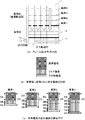
図1(a)は、フレーム転送方式CCDの構成を示した図である。フレーム転送方式CCDは、入射された光を電荷に変換する撮像部11と、光が遮蔽された蓄積部12と、蓄積部から転送された電荷を出力回路14へ転送する水平転送部13と、電荷を電圧に変換し外部へ出力する出力回路14とからなる。撮像部11は垂直転送部を兼ねており、撮像期間に撮像部11で変換された電荷は、撮像期間後に素早く蓄積部12に転送され、これ以上光が入射されるのを防ぐ構造になっている。
FIG. 1A is a diagram showing the configuration of a frame transfer type CCD. The frame transfer type CCD includes an
図1(b)は、蓄積部12に蓄積された各画素における信号電荷の内訳を示した図である。蓄積部12に蓄積された各画素における信号電荷は、画素電荷、スミア雑音、その他の雑音に分けられる。画素電荷は、撮像期間に入射された光によって発生した電荷量であり、これが真の画像情報である。
FIG. 1B is a diagram showing a breakdown of signal charges in each pixel accumulated in the
スミア雑音は、撮像期間直後、撮像部11から蓄積部12へ電荷が転送される転送期間中に、撮像部11に入射された光によって生成された電荷が蓄積されたものである。すなわち、このスミア雑音は、フレーム転送方式CCDの撮像部11が垂直転送部を兼用する構造のために発生するもので、撮像期間外に発生した不要な信号電荷である。
その他の雑音は、CCD内で発生する様々な雑音であり、製造プロセスや基板の結晶品質などに起因する固定パターン雑音や、各素子の揺らぎによるランダム雑音を含む。
The smear noise is a result of accumulating charges generated by light incident on the
Other noises are various noises generated in the CCD, and include fixed pattern noises caused by the manufacturing process and crystal quality of the substrate, and random noises caused by fluctuations of each element.
図1(c)は、図1(a)に示した画素1、画素2、画素3、画素4それぞれにおいて、図1(b)の各信号電荷の占める割合を示した図である。この図から撮像部11から蓄積部12へ転送する距離が長くなるほど、スミア雑音が多くなることが見て取れる。これは、転送距離が長ければ転送期間中に光にさらされる時間も長くなるからである。
FIG. 1C is a diagram showing the proportion of each signal charge in FIG. 1B in each of the
先に説明したように、画素電荷は、撮像期間中に入射された光に応じて発生するのに対し、スミア雑音は、転送期間中に入射された光に応じて発生する。したがって、スミア雑音の大きさは、出力された信号電荷から撮像時間と転送時間とをもとに予測することが可能である。 As described above, the pixel charge is generated according to the light incident during the imaging period, while the smear noise is generated according to the light incident during the transfer period. Therefore, the magnitude of smear noise can be predicted based on the imaging time and transfer time from the output signal charge.
以下、図1(c)を用いて、各画素のスミア雑音の予測方法について説明する。ここでは、撮像期間と転送期間で同じ強度の光が撮像部11に入射されていると仮定する。スミア雑音を予測する場合、蓄積部12に最も近い画素1から予測する。画素1の画素電荷の大きさ1Aとスミア雑音の大きさ1Bとの比(1A:1B)は、撮像時間TAと1画素分を垂直転送するのにかかる時間TBとの比(TA:TB)で表すことができる。したがって、画素1の信号電荷の大きさを1S、その他の雑音の大きさを1Nとすると、画素1におけるスミア雑音の大きさ1Bは次式のようになる。
1B=TB・(1S−1N)/(TA+TB) ・・・ (1)
Hereinafter, a method for predicting smear noise of each pixel will be described with reference to FIG. Here, it is assumed that light having the same intensity is incident on the
1B = TB · (1S-1N) / (TA + TB) (1)
次に、画素2のスミア雑音を予測する。画素2に蓄積された電荷は、撮像部11の画素1を通って蓄積部12に転送される。したがって、蓄積部12に転送された段階で画素2の信号電荷2Sには、画素1のスミア雑音も含まれる。一方、画素2の画素電荷の大きさ2Aと画素2で発生するスミア雑音の大きさ2Bとの比は、画素1と同様、撮像時間TAと1画素分を垂直転送するのにかかる時間TBとの比(TA:TB)で表すことができる。したがって、その他の雑音の大きさを2Nとすると、画素2におけるスミア雑音の大きさ2Bは次式のようになる。
2B=TB・(2S−2N−1B)/(TA+TB) ・・・ (2)
Next, the smear noise of the
2B = TB · (2S-2N-1B) / (TA + TB) (2)
画素3についても画素2と同様に求めることができる。すなわち、画素3は、撮像部11の画素1、画素2を通って蓄積部12に転送されるため、画素1と画素2のスミア雑音1B、2Bが画素3の信号電荷3Sに含まれる。そして、画素3の画素電荷の大きさ3Aと画素3で発生するスミア雑音の大きさ3Bとの比は、撮像時間TAと1画素分を垂直転送するのにかかる時間TBとの比(TA:TB)で表すことできるので、画素3におけるその他の雑音の大きさを3Nとすると、画素3におけるスミア雑音の大きさ3Bは次式のようになる。
3B=TB・(3S−3N−1B−2B)/(TA+TB) ・・・ (3)
The pixel 3 can be obtained similarly to the
3B = TB · (3S-3N-1B-2B) / (TA + TB) (3)
以後、垂直方向に順次、各画素のスミア雑音を予測していく。予測の方法は、予測対象となる画素の信号電荷から、その画素のその他の雑音と、蓄積部12まで転送される間に通過する撮像部11の各画素のスミア雑音とを差し引き、差し引いた値に対して、撮像時間TAと1画素分を垂直転送するのにかかる時間TBとの比(TA:TB)で比例配分する。
Thereafter, the smear noise of each pixel is predicted sequentially in the vertical direction. The prediction method is a value obtained by subtracting and subtracting other noise of the pixel and smear noise of each pixel of the
なお、以上の説明の中で、その他の雑音を差し引いたが、その他の雑音は、予測値として任意に設定した値を差し引いてもよい。この任意に値はゼロも含まれる。また、その他の雑音のうち、固定パターン雑音については測定することが可能であるため、測定によって求められた固定パターン雑音をその他の雑音として差し引いてもよい。もしくは、測定によって求められた固定パターン雑音に、ランダム雑音として任意に設定された値が足し合わされたものを、その他の雑音として差し引いてもよい。これにより、予測したスミア雑音は正確な値ではない可能性もあるが、本発明の実施形態では、スミア雑音の予測値を求めることが重要であり、正確な値を求める必要はない。 In the above description, other noise is subtracted, but for other noise, a value arbitrarily set as a predicted value may be subtracted. This optional value includes zero. Moreover, since it is possible to measure fixed pattern noise among other noises, the fixed pattern noise obtained by measurement may be subtracted as other noise. Alternatively, a value obtained by adding a value arbitrarily set as random noise to the fixed pattern noise obtained by measurement may be subtracted as other noise. Thus, the predicted smear noise may not be an accurate value, but in the embodiment of the present invention, it is important to obtain a predicted value of the smear noise, and it is not necessary to obtain an accurate value.
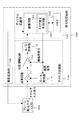
次に、本発明の実施の形態に係る信号処理回路100について説明する。図2は、本発明の実施の形態に係る信号処理回路100の構成を示すブロック図である。信号処理回路100は、フレーム転送方式CCD200から入力されたアナログ入力信号を増幅し、ディジタル信号に変換するアナログ回路部110と、アナログ回路部で変換されたディジタル信号に対しディジタル処理を行うディジタル回路部120と、フレーム転送方式CCD200を駆動する駆動回路部130を具備している。なお、信号処理回路100とフレーム転送方式CCD200により、ディジタルカメラを構成することができる。
Next, the
アナログ回路部110は、アナログ入力信号を被減算数として減算処理を行う減算回路111と、増幅率が変更可能で、減算回路111で減算処理されたアナログ信号を増幅する可変増幅回路112と、可変増幅回路112で増幅されたアナログ信号をディジタル信号に変換するA/D変換器113と、を具備している。また、ディジタル回路部120より入力された減算信号をアナログ信号に変換するD/A変換器114も備え、D/A変換器114の出力は減算数として減算回路111に入力される。さらに、ディジタル回路部120より入力された増幅度信号が可変増幅回路112に入力され、可変増幅回路112は増幅度信号で示された増幅度に従って増幅処理を行う。
The
ディジタル回路部120は、アナログ回路部より入力されたディジタル信号やその他のディジタル信号に対し、所定の処理を施す論理回路121と、一時的にデータを記憶するメモリ122と、を備える。また、論理回路121は、スミア雑音予測回路123を含み、スミア雑音の大きさを予測する。スミア雑音予測回路123で予測された値は、減算信号としてアナログ回路部110へ出力される。また、スミア雑音の予測値にもとに、増幅回路の出力振幅が前記A/D変換器の入力レベル範囲を超えない範囲で増幅度信号の値が決定される。
The
駆動回路部130は、フレーム転送方式CCD200の駆動信号を生成するほか、フレーム転送方式CCD200から出力されているデータがどの画素位置のものであるかを示すアドレスも生成する。このアドレスはディジタル回路部120に入力される。また、フレーム転送方式CCD200を駆動するためのパラメータである撮像時間TAと転送時間TBも駆動回路部130からディジタル回路部120へ入力される。
The
信号処理回路100の動作を説明する。まず、駆動回路部130の駆動信号に従って、フレーム転送方式CCD200で撮像が行われた後、フレーム転送方式CCD200内で信号電荷が信号電圧に変換され、この信号電圧がアナログ入力信号として1画素ずつ出力される。そして、このアナログ入力信号は、はじめは減算回路111による減算処理がなされずに可変増幅回路112によって増幅され、A/D変換器によってディジタル信号に変換された後、ディジタル回路部120に入力される。
The operation of the
論理回路121に備えられたスミア雑音予測回路123は、アナログ回路部110より入力されたディジタル信号と、駆動回路部130から入力された撮像時間TA及び転送時間TBをもとに、先に述べたスミア雑音の予測方法により、各画素のスミア雑音を予測する。このスミア雑音の予測値は一旦メモリ122に記憶される。
The smear
以上の動作は、フレーム転送方式CCDのすべての画素について、その信号電圧が読み出されるまで行われ、最終的に全画素のスミア雑音の予測値がメモリ122に記憶される。
The above operation is performed until the signal voltage is read for all the pixels of the frame transfer type CCD, and finally the predicted value of the smear noise of all the pixels is stored in the
次に、駆動回路部130の駆動信号に従って、再度フレーム転送方式CCD200で撮像が行われ、各画素の信号電圧がアナログ入力信号として出力される。この時、論理回路121は、駆動回路部130から出力されるアドレスにしたがって、フレーム転送方式CCD200から出力されているアナログ入力信号の画素と同じ画素のスミア雑音を、メモリ122から読み出し、それを減算信号として出力する。すなわち、信号電荷の大きさと撮像時間、転送時間に基いて求めた各画素のスミア雑音を、現在入力されているアナログ入力信号がフレーム転送方式CCD200のどの画素から出力されたかに応じて選択し、減算信号として出力することになる。つまり、減算信号は、アナログ入力信号の属性である、信号電荷の大きさ、撮像時間、転送時間、及び現在入力されているアナログ入力信号がフレーム転送方式CCD200のどの画素から出力されたかによって、適応的に変化する。
Next, imaging is performed again by the
減算信号はD/A変換器114によってアナログ信号に変換され、このアナログ信号を減算数として
減算回路111に入力する。減算回路は被減算数であるアナログ入力信号から減算数を減算する。すなわち、アナログ入力信号からスミア雑音が除去されることになり、減算後のアナログ信号は、ほぼ真の画像情報を表す画素電荷信号で構成される。
The subtraction signal is converted into an analog signal by the D /
Input to the
減算後のアナログ信号は、可変増幅回路112に入力され、可変増幅回路112の出力がA/D変換器113の入力範囲を超えない範囲で決定された増幅度に従って増幅される。そして、増幅されたアナログ信号をA/D変換器113によってディジタル信号に変換し、ディジタル回路部120へ出力され、所定の画像処理演算が施される。
このように、不要な変動信号を可変増幅回路の前段で減算することにより、より精度の高い信号処理が実現できる。
The subtracted analog signal is input to the
As described above, by subtracting the unnecessary fluctuation signal in the previous stage of the variable amplifier circuit, more accurate signal processing can be realized.
したがって、以上の構成によれば、信号電荷の大きさ、撮像時間、転送時間、及び現在入力されているアナログ入力信号が撮像装置のどの画素から出力されたかによって変化するスミア雑音を適応的に予測し、これを可変増幅回路で増幅する前にアナログ入力信号から除去できる。これにより、可変増幅回路で増幅する信号は、真の画像情報を表す画素電荷信号でほぼ構成された信号となるため、より精度の高い信号処理が実現できる。 Therefore, according to the above configuration, smear noise that varies depending on the magnitude of signal charge, imaging time, transfer time, and from which pixel of the imaging device the currently input analog input signal is output is adaptively predicted. This can be removed from the analog input signal before it is amplified by the variable amplifier circuit. As a result, the signal amplified by the variable amplifier circuit becomes a signal substantially composed of a pixel charge signal representing true image information, so that more accurate signal processing can be realized.
なお、この実施の形態において、フレーム転送方式CCDについて説明したが、これに限るものではなく、他の撮像装置で発生したスミア雑音を予測し、アナログ入力信号から減算するように構成してもよい。この場合、スミア雑音の予測方法は、撮像装置の構成に合わせて決定される。 In this embodiment, the frame transfer type CCD has been described. However, the present invention is not limited to this, and a smear noise generated in another imaging apparatus may be predicted and subtracted from the analog input signal. . In this case, the smear noise prediction method is determined according to the configuration of the imaging apparatus.
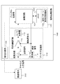
図3は、別の実施の形態に係る信号処理回路100の構成を示したブロック図である。この信号処理回路100は、撮像素子300から入力されたアナログ信号を、ディジタル回路部で予測した固定パターン雑音を減算した上で増幅し、ディジタル信号に変換する信号処理回路に関する。この構成は、図2に示した信号処理回路100の構成と類似しているので、この実施の形態に特徴的な点のみを説明し、それ以外の説明は省略する。なお、本実施の形態においても、信号処理回路100と撮像素子300により、ディジタルカメラを構成することができる。
FIG. 3 is a block diagram showing a configuration of a
光を遮蔽した状態で、駆動回路部130により生成された駆動信号により、撮像素子300が駆動されると、撮像素子300から出力されるアナログ入力信号は、固定パターン雑音とランダム雑音とが足し合わされたものになる。そこで、まずこのようなアナログ入力信号をアナログ回路部110に入力し、減算回路111による減算処理は行わず、可変増幅回路112、A/D変換器113を通して、ディジタル信号に変換して、ディジタル回路部120に入力する。
When the
論理回路121では、撮像素子300の全画素に対して、入力されたディジタル信号から固定パターン雑音を予測し、メモリ122の固定パターン雑音記憶領域124に記憶する。固定パターン雑音の予測方法としては、ランダム雑音をある一定の値と仮定してディジタル信号から差し引く方法がある。また、入力されたディジタル信号をそのまま固定パターン雑音の予測値としてもよい。また、光を遮蔽した状態のまま、撮像素子300を複数回撮像し、固定パターン雑音とランダム雑音からなる複数枚の画像データを取得した上で、複数の画像データにLPF(Low Path Filter)を通すことにより、ランダム雑音を除去して固定パターン雑音を予測してもよい。
In the
つづいて、撮像素子300によって画像を撮像する場合、論理回路121は駆動回路部130から出力されるアドレスにしたがって、撮像素子300から出力されているアナログ入力信号の画素と同じ画素の固定パターン雑音を固定パターン雑音記憶領域124から読み出し、それを減算信号として出力する。すなわち、減算信号は、現在入力されているアナログ入力信号が撮像素子300のどの画素から出力されたか、というアナログ入力信号の属性によって、適応的に変化する。
Subsequently, when an image is picked up by the
この減算信号はD/A変換器114を通って減算数として減算回路に入力され、減算回路でアナログ入力信号から不要な信号(この実施の形態では固定パターン雑音)を減算した後、減算後のアナログ信号が、可変増幅回路112でA/D変換器113の入力範囲を超えない範囲で決定された増幅度信号に基いて増幅され、A/D変換器113によってディジタル信号に変換されて、ディジタル回路部120に出力される。
This subtraction signal is input as a subtraction number to the subtraction circuit through the D /
したがって、以上の構成によれば、撮像素子300に固有の固定パターン雑音を適応的に予測し、これを可変増幅回路で増幅する前にアナログ入力信号から除去できる。これにより、可変増幅回路で増幅する信号は、真の画像情報を表す画素電荷信号でほぼ構成された信号となるため、より精度の高い信号処理が実現できる。
Therefore, according to the above configuration, it is possible to adaptively predict the fixed pattern noise unique to the
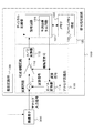
図4は、さらに別の実施の形態に係る信号処理回路100の構成を示したブロック図である。この信号処理回路100は、入力画像データと予測画像データから差分画像データを算出し、この差分画像データに対して演算を行う。従来は、差分画像データの算出をディジタル回路部で行っていたが、本実施の形態では、撮像素子300から入力されたアナログ信号に対して、ディジタル回路部で生成した予測画像信号を減算して差分画像信号を得、この差分画像信号を増幅して、ディジタル信号に変換する。この構成は、図2に示した信号処理回路100の構成と類似しているので、この実施の形態に特徴的な点のみを説明し、それ以外の説明は省略する。なお、本実施の形態においても、信号処理回路100と撮像素子300により、ディジタルカメラを構成することができる。
FIG. 4 is a block diagram showing a configuration of a
ディジタル回路部120のメモリ122には、フレームメモリ領域126が設けてあり、そこにあらかじめ複数枚の画像データが参照画像データとして記憶されている。また、論理回路121には、予測画像生成回路125が備えられている。
A frame memory area 126 is provided in the
撮像素子300により出力される画像信号に対し、参照画像による予測処理を行わない場合、アナログ回路部110は減算回路111による減算処理を行うことなく、アナログ入力信号をそのまま可変増幅回路112で増幅後、A/D変換器113でディジタル信号に変換して、ディジタル回路部120へ入力する。
一方、撮像素子300により出力される画像信号に対し、参照画像による予測処理を行う場合は、以下のような動作を行う。
When the prediction process using the reference image is not performed on the image signal output from the
On the other hand, when performing prediction processing using a reference image on an image signal output from the
まず、駆動回路部130により生成されたアドレスにしたがって、予測画像生成回路125は、現在、撮像素子300より入力されているアナログ入力信号が撮像素子300のどの領域から出力されたかを判断し、あらかじめフレームメモリ領域126に記憶されている参照画像データから、必要な領域の画像データを1つ、或いは複数読み出し、所定の処理を施して、予測画像データを生成する。そして、論理回路121は、駆動回路部130により生成されたアドレスにより、現在入力されているアナログ入力信号の画素位置に合わせて、予測画像の中から対応する画素データを選択する。この画素データに相当する信号が減算信号としてアナログ回路部110に出力される。したがって、この減算信号は、現在入力されているアナログ入力信号が撮像素子300のどの領域、およびどの画素から出力されたか、というアナログ入力信号の属性によって、適応的に変化する。
First, according to the address generated by the
この減算信号はD/A変換器114を通って減算数として減算回路に入力される。減算回路は、アナログ入力信号から予測画像データに相当する信号を減算して差分画像データを求める。この差分画像データが、可変増幅回路112でA/D変換器113の入力範囲を超えない範囲で決定された増幅度信号に基いて増幅され、A/D変換器113によってディジタル信号に変換されて、ディジタル回路部120に出力される。
This subtraction signal passes through the D /
したがって、以上の構成によれば、予測画像データを適応的に生成し、これを可変増幅回路で増幅する前にアナログ入力信号から除去して差分画像データを求めることができる。この差分画像データを可変増幅回路で増幅するため、差分画像データに対して、より精度の高い信号処理が実現できる。
以上、本発明を実施の形態をもとに説明した。これらの実施の形態は例示であり、それらの各構成要素の組合せにいろいろな変形例が可能なこと、またそうした変形例も本発明の範囲にあることは当業者に理解されるところである。
Therefore, according to the above configuration, the predicted image data can be adaptively generated and removed from the analog input signal before being amplified by the variable amplifier circuit, thereby obtaining the difference image data. Since the difference image data is amplified by the variable amplification circuit, more accurate signal processing can be realized for the difference image data.
The present invention has been described based on the embodiments. It is to be understood by those skilled in the art that these embodiments are exemplifications, and that various modifications can be made to combinations of the respective constituent elements, and such modifications are within the scope of the present invention.
例えば、図2の信号処理回路100と図3の信号処理回路100を組み合わせて信号処理回路を構成してもよい。この場合、スミア雑音と固定パターン雑音の両方を、実施の形態で説明した方法に基いてディジタル回路部120で予測し、これらの和を減算信号として入力信号から除去できる。また、入力信号に含まれる雑音において、固定パターン雑音がスミア雑音と比して無視できるほど小さい場合は、スミア雑音のみを予測し、これを減算信号としてもよい。或いは、スミア雑音が固定パターン雑音と比して無視できるほど小さい場合は、固定パターン雑音のみを予測して、これを減算信号としてもよい。この構成によれば、入力を発生した系に応じて雑音信号を予測するので、様々な入力に対してより精度の高い信号処理が実現できる。
For example, the
100 信号処理回路、
110 アナログ回路部、
111 減算回路、
112 可変増幅回路、
113 A/D変換器、
114 D/A変換器、
120 ディジタル回路部、
121 論理回路、
122 メモリ、
123 スミア雑音予測回路、
124 固定パターン雑音記憶領域、
125 予測画像生成回路、
126 フレームメモリ領域、
130 駆動回路部、
200 フレーム転送方式CCD、
300 撮像素子。
100 signal processing circuit,
110 Analog circuit part,
111 subtraction circuit,
112 variable amplifier circuit,
113 A / D converter,
114 D / A converter,
120 digital circuit section,
121 logic circuit,
122 memory,
123 smear noise prediction circuit,
124 fixed pattern noise storage area,
125 prediction image generation circuit,
126 frame memory area,
130 drive circuit section,
200 frame transfer CCD,
300 Image sensor.
Claims (6)
前記減算回路の出力を増幅する増幅回路と、
前記増幅回路の出力をディジタル信号に変換するA/D変換器と、
前記A/D変換器で生成されたディジタル信号を処理するディジタル回路部と、
を具備し、
前記ディジタル回路部は、前記入力信号の属性によって変化する不要な信号を生成し、この不要な信号はアナログ信号に変換された後、前記減算回路に入力されることを特徴とした信号処理回路。 A subtraction circuit that performs subtraction processing from an input signal that is an analog signal;
An amplification circuit for amplifying the output of the subtraction circuit;
An A / D converter for converting the output of the amplifier circuit into a digital signal;
A digital circuit section for processing a digital signal generated by the A / D converter;
Comprising
The signal processing circuit, wherein the digital circuit section generates an unnecessary signal that changes according to an attribute of the input signal, and the unnecessary signal is converted into an analog signal and then input to the subtraction circuit.
前記メモリに複数枚の画像データを参照画像データとして記憶し、
前記論理回路は前記参照画像データから予測画像データを生成し、
前記不要な信号はこの予測画像データに相当する信号が含まれることを特徴とする請求項1又は2に記載の信号処理回路。 The digital circuit unit includes a logic circuit and a memory,
Storing a plurality of pieces of image data as reference image data in the memory;
The logic circuit generates predicted image data from the reference image data;
The signal processing circuit according to claim 1, wherein the unnecessary signal includes a signal corresponding to the predicted image data.
前記減算回路の出力を増幅する増幅回路と、
前記雑音に相当する信号を生成する雑音予測回路と、
を備え、前記雑音予測回路は、前記雑音に相当する信号を、前記入力信号を発生した系に応じて定めることを特徴とする信号処理回路。 A subtraction circuit that subtracts a signal corresponding to noise from an input signal that is an analog signal;
An amplification circuit for amplifying the output of the subtraction circuit;
A noise prediction circuit for generating a signal corresponding to the noise;
And the noise prediction circuit determines a signal corresponding to the noise according to a system in which the input signal is generated.
Priority Applications (4)
| Application Number | Priority Date | Filing Date | Title |
|---|---|---|---|
| JP2004102448A JP2005294888A (en) | 2004-03-31 | 2004-03-31 | Signal processing circuit |
| KR1020050025816A KR20060044894A (en) | 2004-03-31 | 2005-03-29 | Signal processing circuit and imaging device for performing high precision signal processing |
| CNA2005100627841A CN1678028A (en) | 2004-03-31 | 2005-03-30 | High-precision signal processing circuit and an image capturing apparatus |
| US11/092,813 US20050219389A1 (en) | 2004-03-31 | 2005-03-30 | Efficient fluctuating signal subtraction in a signal processing circuit and an image capturing apparatus |
Applications Claiming Priority (1)
| Application Number | Priority Date | Filing Date | Title |
|---|---|---|---|
| JP2004102448A JP2005294888A (en) | 2004-03-31 | 2004-03-31 | Signal processing circuit |
Publications (1)
| Publication Number | Publication Date |
|---|---|
| JP2005294888A true JP2005294888A (en) | 2005-10-20 |
Family
ID=35050311
Family Applications (1)
| Application Number | Title | Priority Date | Filing Date |
|---|---|---|---|
| JP2004102448A Withdrawn JP2005294888A (en) | 2004-03-31 | 2004-03-31 | Signal processing circuit |
Country Status (4)
| Country | Link |
|---|---|
| US (1) | US20050219389A1 (en) |
| JP (1) | JP2005294888A (en) |
| KR (1) | KR20060044894A (en) |
| CN (1) | CN1678028A (en) |
Cited By (1)
| Publication number | Priority date | Publication date | Assignee | Title |
|---|---|---|---|---|
| KR100806438B1 (en) | 2005-10-28 | 2008-02-21 | 가부시끼가이샤 도시바 | Solid state image pickup device |
Families Citing this family (3)
| Publication number | Priority date | Publication date | Assignee | Title |
|---|---|---|---|---|
| KR101022832B1 (en) * | 2009-11-16 | 2011-03-17 | 연세대학교 산학협력단 | Smear removal apparatus and method for ccd sensor |
| CN101794727B (en) * | 2010-01-29 | 2012-05-30 | 浙江大学 | Distributed cancellation method of integrated circuit substrate noise and circuit |
| CN121007818A (en) * | 2025-08-25 | 2025-11-25 | 合肥合安智为科技有限公司 | Methods and devices for detecting spatial particulate matter concentration in industrial and mining environments |
Family Cites Families (6)
| Publication number | Priority date | Publication date | Assignee | Title |
|---|---|---|---|---|
| KR920010512B1 (en) * | 1989-01-27 | 1992-11-30 | 가부시끼가이샤 히다찌세이사꾸쇼 | Image pick-up device |
| TW297202B (en) * | 1993-10-13 | 1997-02-01 | Rca Thomson Licensing Corp | |
| US6285710B1 (en) * | 1993-10-13 | 2001-09-04 | Thomson Licensing S.A. | Noise estimation and reduction apparatus for video signal processing |
| US6061092A (en) * | 1997-12-05 | 2000-05-09 | Intel Corporation | Method and apparatus for dark frame cancellation for CMOS sensor-based tethered video peripherals |
| US6750910B1 (en) * | 1998-07-15 | 2004-06-15 | Texas Instruments Incorporated | Optical black and offset correction in CCD signal processing |
| FR2856547B1 (en) * | 2003-06-23 | 2005-09-23 | St Microelectronics Sa | METHOD FOR PROCESSING THE BLACK LEVEL OF A PIXEL MATRIX OF AN IMAGE SENSOR, AND CORRESPONDING SENSOR |
-
2004
- 2004-03-31 JP JP2004102448A patent/JP2005294888A/en not_active Withdrawn
-
2005
- 2005-03-29 KR KR1020050025816A patent/KR20060044894A/en not_active Ceased
- 2005-03-30 CN CNA2005100627841A patent/CN1678028A/en active Pending
- 2005-03-30 US US11/092,813 patent/US20050219389A1/en not_active Abandoned
Cited By (1)
| Publication number | Priority date | Publication date | Assignee | Title |
|---|---|---|---|---|
| KR100806438B1 (en) | 2005-10-28 | 2008-02-21 | 가부시끼가이샤 도시바 | Solid state image pickup device |
Also Published As
| Publication number | Publication date |
|---|---|
| CN1678028A (en) | 2005-10-05 |
| KR20060044894A (en) | 2006-05-16 |
| US20050219389A1 (en) | 2005-10-06 |
Similar Documents
| Publication | Publication Date | Title |
|---|---|---|
| KR101105516B1 (en) | Solid-state image pickup apparatus and image pickup method | |
| JP4998056B2 (en) | Imaging apparatus, imaging system, and imaging method | |
| JP5610961B2 (en) | Solid-state imaging device and driving method of solid-state imaging device | |
| JP5528283B2 (en) | Solid-state imaging device | |
| CN101072303A (en) | Image pickup device and image pickup apparatus | |
| JP6896788B2 (en) | Imaging equipment, imaging methods, computer programs and storage media | |
| CN100454984C (en) | Signal processing device and signal processing method for solid-state imaging element | |
| JPH11331592A (en) | Image reading device and computer readable storage medium | |
| JP5805260B2 (en) | Solid-state imaging device and driving method of solid-state imaging device | |
| JPH08331463A (en) | Smear correction of CCD imager using active pixels | |
| JP5222068B2 (en) | Imaging device | |
| JP5528282B2 (en) | Solid-state imaging device | |
| JP2017028416A (en) | Image sensor | |
| US11778346B2 (en) | Image processing device, image processing method, and storage medium | |
| JP2005294888A (en) | Signal processing circuit | |
| US10560653B2 (en) | Image sensing apparatus and control method for performing analog-to-digital conversion | |
| JP6160139B2 (en) | Imaging apparatus and method | |
| JP2003259234A (en) | CMOS image sensor | |
| JP5172283B2 (en) | Stereo image processing apparatus, stereo image processing method, and program | |
| JP2016523474A (en) | CMOS sensor with standard photosite | |
| JP2006060628A (en) | Solid-state image pickup device | |
| JP5956856B2 (en) | Imaging device and imaging system | |
| JP4368396B2 (en) | AD converter | |
| JP4322258B2 (en) | Noise processing apparatus and imaging apparatus | |
| JP2018107527A (en) | Imaging apparatus and control method thereof |
Legal Events
| Date | Code | Title | Description |
|---|---|---|---|
| A621 | Written request for application examination |
Free format text: JAPANESE INTERMEDIATE CODE: A621 Effective date: 20051101 |
|
| A761 | Written withdrawal of application |
Free format text: JAPANESE INTERMEDIATE CODE: A761 Effective date: 20080526 |