JP2005294588A - Organic semiconductor material, organic semiconductor structure and organic semiconductor device - Google Patents
Organic semiconductor material, organic semiconductor structure and organic semiconductor device Download PDFInfo
- Publication number
- JP2005294588A JP2005294588A JP2004108528A JP2004108528A JP2005294588A JP 2005294588 A JP2005294588 A JP 2005294588A JP 2004108528 A JP2004108528 A JP 2004108528A JP 2004108528 A JP2004108528 A JP 2004108528A JP 2005294588 A JP2005294588 A JP 2005294588A
- Authority
- JP
- Japan
- Prior art keywords
- organic semiconductor
- organic
- liquid crystal
- semiconductor layer
- semiconductor material
- Prior art date
- Legal status (The legal status is an assumption and is not a legal conclusion. Google has not performed a legal analysis and makes no representation as to the accuracy of the status listed.)
- Granted
Links
Images
Classifications
-
- H—ELECTRICITY
- H10—SEMICONDUCTOR DEVICES; ELECTRIC SOLID-STATE DEVICES NOT OTHERWISE PROVIDED FOR
- H10K—ORGANIC ELECTRIC SOLID-STATE DEVICES
- H10K85/00—Organic materials used in the body or electrodes of devices covered by this subclass
- H10K85/60—Organic compounds having low molecular weight
- H10K85/649—Aromatic compounds comprising a hetero atom
- H10K85/655—Aromatic compounds comprising a hetero atom comprising only sulfur as heteroatom
-
- H—ELECTRICITY
- H10—SEMICONDUCTOR DEVICES; ELECTRIC SOLID-STATE DEVICES NOT OTHERWISE PROVIDED FOR
- H10K—ORGANIC ELECTRIC SOLID-STATE DEVICES
- H10K85/00—Organic materials used in the body or electrodes of devices covered by this subclass
- H10K85/10—Organic polymers or oligomers
- H10K85/111—Organic polymers or oligomers comprising aromatic, heteroaromatic, or aryl chains, e.g. polyaniline, polyphenylene or polyphenylene vinylene
- H10K85/113—Heteroaromatic compounds comprising sulfur or selene, e.g. polythiophene
-
- H—ELECTRICITY
- H10—SEMICONDUCTOR DEVICES; ELECTRIC SOLID-STATE DEVICES NOT OTHERWISE PROVIDED FOR
- H10K—ORGANIC ELECTRIC SOLID-STATE DEVICES
- H10K85/00—Organic materials used in the body or electrodes of devices covered by this subclass
- H10K85/731—Liquid crystalline materials
-
- H—ELECTRICITY
- H10—SEMICONDUCTOR DEVICES; ELECTRIC SOLID-STATE DEVICES NOT OTHERWISE PROVIDED FOR
- H10K—ORGANIC ELECTRIC SOLID-STATE DEVICES
- H10K10/00—Organic devices specially adapted for rectifying, amplifying, oscillating or switching; Organic capacitors or resistors having potential barriers
- H10K10/40—Organic transistors
- H10K10/46—Field-effect transistors, e.g. organic thin-film transistors [OTFT]
- H10K10/462—Insulated gate field-effect transistors [IGFETs]
- H10K10/466—Lateral bottom-gate IGFETs comprising only a single gate
-
- Y—GENERAL TAGGING OF NEW TECHNOLOGICAL DEVELOPMENTS; GENERAL TAGGING OF CROSS-SECTIONAL TECHNOLOGIES SPANNING OVER SEVERAL SECTIONS OF THE IPC; TECHNICAL SUBJECTS COVERED BY FORMER USPC CROSS-REFERENCE ART COLLECTIONS [XRACs] AND DIGESTS
- Y02—TECHNOLOGIES OR APPLICATIONS FOR MITIGATION OR ADAPTATION AGAINST CLIMATE CHANGE
- Y02E—REDUCTION OF GREENHOUSE GAS [GHG] EMISSIONS, RELATED TO ENERGY GENERATION, TRANSMISSION OR DISTRIBUTION
- Y02E10/00—Energy generation through renewable energy sources
- Y02E10/50—Photovoltaic [PV] energy
- Y02E10/549—Organic PV cells
-
- Y—GENERAL TAGGING OF NEW TECHNOLOGICAL DEVELOPMENTS; GENERAL TAGGING OF CROSS-SECTIONAL TECHNOLOGIES SPANNING OVER SEVERAL SECTIONS OF THE IPC; TECHNICAL SUBJECTS COVERED BY FORMER USPC CROSS-REFERENCE ART COLLECTIONS [XRACs] AND DIGESTS
- Y10—TECHNICAL SUBJECTS COVERED BY FORMER USPC
- Y10T—TECHNICAL SUBJECTS COVERED BY FORMER US CLASSIFICATION
- Y10T428/00—Stock material or miscellaneous articles
- Y10T428/31504—Composite [nonstructural laminate]
Landscapes
- Chemical & Material Sciences (AREA)
- Engineering & Computer Science (AREA)
- Materials Engineering (AREA)
- Crystallography & Structural Chemistry (AREA)
- Physics & Mathematics (AREA)
- Spectroscopy & Molecular Physics (AREA)
- Thin Film Transistor (AREA)
- Heterocyclic Carbon Compounds Containing A Hetero Ring Having Oxygen Or Sulfur (AREA)
- Electroluminescent Light Sources (AREA)
Abstract
【課題】 少なくとも常温を含む広い温度範囲で液晶相を示すと共に、高い電荷移動度の発現を可能にする有機半導体材料及び有機半導体構造物並びに有機半導体装置を提供する。
【解決手段】 下記化学式1で表されるクォーターチオフェン骨格を有する有機半導体材料により、上記課題を解決する。式中、R1はC1〜C20のアルキル基又は水素であり、R2はC1〜C20のアルキル基又は水素である。本発明の有機半導体構造物は、少なくとも−40〜+90℃の温度範囲で高次のスメクティック液晶相を有する有機半導体層を備え、且つその有機半導体層は少なくとも常温領域で10−1cm2/V・s以上の電荷移動度を有する。
【化1】
The above problem is solved by an organic semiconductor material having a quarterthiophene skeleton represented by the following chemical formula 1. In the formula, R1 is a C1-C20 alkyl group or hydrogen, and R2 is a C1-C20 alkyl group or hydrogen. The organic semiconductor structure of the present invention includes an organic semiconductor layer having a high-order smectic liquid crystal phase in a temperature range of at least −40 to + 90 ° C., and the organic semiconductor layer is at least 10 −1 cm 2 / V in a normal temperature region. -It has charge mobility of s or more.
[Chemical 1]
Description
本発明は、少なくとも常温を含む広い温度範囲で液晶相を示す有機半導体材料、有機半導体構造物及び有機半導体装置に関するものである。 The present invention relates to an organic semiconductor material, an organic semiconductor structure, and an organic semiconductor device that exhibit a liquid crystal phase in a wide temperature range including at least room temperature.
近年、有機半導体材料を用いた有機半導体構造物についての研究が注目され、各種のデバイスへの応用が期待されている。そうした応用として、フレキシブルディスプレイ装置等に利用可能な薄膜トランジスタ(有機TFTともいう。)、発光素子、太陽電池等が研究対象となっている。 In recent years, research on organic semiconductor structures using organic semiconductor materials has attracted attention, and application to various devices is expected. As such applications, thin film transistors (also referred to as organic TFTs), light-emitting elements, solar cells, and the like that can be used in flexible display devices and the like have been studied.
有機半導体構造物が実用レベルで利用されるためには、広い使用温度範囲において高い電荷移動度を示すことが必要であると共に、広い面積で均一且つ柔軟な分子配向薄膜が作製されることが必要である。したがって、常温を含む広い使用温度範囲(−40〜+90℃程度)で液晶相を示すと共に、その液晶相が高い電荷移動度を有していることが望ましい。 In order to use an organic semiconductor structure at a practical level, it is necessary to exhibit high charge mobility in a wide use temperature range, and it is necessary to produce a uniform and flexible molecular alignment thin film in a wide area. It is. Accordingly, it is desirable that the liquid crystal phase is exhibited in a wide use temperature range (about −40 to + 90 ° C.) including normal temperature, and the liquid crystal phase has high charge mobility.
従来においては、例えば、フェニルベンゾチアゾール誘導体等の棒状(ロッド状)の液晶性材料が液晶状態で高い電荷移動度を示すことが報告されている(例えば、非特許文献1を参照)。しかし、この液晶性材料は、比較的高い温度で液晶性を示すが、常温を含む広い使用温度範囲(−40〜+90℃程度)では液晶性を示さないものであった。
上述したように、従来の有機半導体材料においては、少なくとも常温を含む広い温度範囲で液晶相を示す有機半導体材料が少ないことから、そのような液晶性有機半導体材料が望まれていると共に、常温を含む広い温度範囲で高い電荷移動度の発現を可能にする有機半導体材料の開発及びその材料を用いた有機半導体構造物が望まれている。 As described above, in conventional organic semiconductor materials, since there are few organic semiconductor materials that exhibit a liquid crystal phase in a wide temperature range including at least room temperature, such liquid crystalline organic semiconductor materials are desired, and room temperature is reduced. Development of an organic semiconductor material capable of developing high charge mobility in a wide temperature range, and an organic semiconductor structure using the material are desired.
本発明は、上述した従来の要請に応えるべくなされたものであって、その目的は、少なくとも常温を含む広い温度範囲で液晶相を示すと共に、高い電荷移動度の発現を可能にする有機半導体材料及びその有機半導体材料からなる有機半導体構造物並びに有機半導体装置を提供することにある。 The present invention has been made to meet the above-described conventional demands, and an object of the present invention is to provide an organic semiconductor material that exhibits a liquid crystal phase in a wide temperature range including at least room temperature and can exhibit high charge mobility. And an organic semiconductor structure and an organic semiconductor device comprising the organic semiconductor material.
上記目的を達成するための本発明の有機半導体材料は、下記化学式1で表されるクォーターチオフェン骨格を有する有機半導体材料であって、式中、R1はC1〜C20のアルキル基又は水素であり、R2はC1〜C20のアルキル基又は水素であることを特徴とする。 The organic semiconductor material of the present invention for achieving the above object is an organic semiconductor material having a quarterthiophene skeleton represented by the following chemical formula 1, wherein R1 is a C1-C20 alkyl group or hydrogen, R2 is a C1-C20 alkyl group or hydrogen.
この発明の有機半導体材料は、少なくとも常温を含む広い温度範囲(−40〜+90℃程度)で液晶相を示すと共に、高い電荷移動度の発現を可能にすることができる。 The organic semiconductor material of the present invention can exhibit a liquid crystal phase in a wide temperature range (about −40 to + 90 ° C.) including at least room temperature and can exhibit high charge mobility.
本発明の有機半導体材料は、上記本発明の有機半導体材料において、前記クォーターチオフェン骨格を有する有機半導体材料が下記化学式2で表されることを特徴とする。 The organic semiconductor material of the present invention is characterized in that, in the organic semiconductor material of the present invention, the organic semiconductor material having the quarterthiophene skeleton is represented by the following chemical formula 2.
この発明の有機半導体材料は、少なくとも−40℃〜+90℃の範囲で高次のスメクティック液晶相を示すことができると共に、この有機半導体材料で有機半導体層を構成すれば10−1cm2/V・s以上の電荷移動度を示すことができる。 The organic semiconductor material of the present invention can exhibit a high-order smectic liquid crystal phase at least in the range of −40 ° C. to + 90 ° C., and 10 −1 cm 2 / V if the organic semiconductor layer is composed of this organic semiconductor material. -Charge mobility of s or more can be shown.
上記目的を達成する本発明の有機半導体構造物は、上記本発明の有機半導体材料からなる有機半導体層を有するものであって、前記有機半導体層は、少なくとも常温領域で高次のスメクティック液晶相を有することを特徴とする。この発明によれば、有機半導体層が少なくとも常温領域で高次のスメクティック液晶相を有するので、広い面積で均一且つ柔軟な分子配向薄膜となり、フレキシブルディスプレイ装置等に利用可能な薄膜トランジスタ等のデバイスに応用することができる。 The organic semiconductor structure of the present invention that achieves the above object has an organic semiconductor layer made of the organic semiconductor material of the present invention, and the organic semiconductor layer has a high-order smectic liquid crystal phase in at least a normal temperature region. It is characterized by having. According to the present invention, since the organic semiconductor layer has a high-order smectic liquid crystal phase in at least a normal temperature region, it becomes a uniform and flexible molecular alignment thin film over a wide area, and is applied to a device such as a thin film transistor that can be used for a flexible display device or the like. can do.
上記目的を達成する本発明の有機半導体装置は、少なくとも基板、ゲート電極、ゲート絶縁層、有機半導体層、ドレイン電極、及びソース電極を有するものであって、前記有機半導体層が、上述した本発明の有機半導体材料で形成されていることを特徴とする。また、本発明の有機半導体装置は、前記有機半導体層が、少なくとも常温領域で10−1cm2/V・s以上の電荷移動度を有することを特徴とする。この発明によれば、広い使用温度範囲において高い電荷移動度を示すので、実用レベルで利用することができる。 An organic semiconductor device of the present invention that achieves the above object has at least a substrate, a gate electrode, a gate insulating layer, an organic semiconductor layer, a drain electrode, and a source electrode, and the organic semiconductor layer is the above-described present invention. It is characterized by being formed of an organic semiconductor material. In the organic semiconductor device of the present invention, the organic semiconductor layer has a charge mobility of 10 −1 cm 2 / V · s or more at least in a normal temperature region. According to the present invention, high charge mobility is exhibited in a wide use temperature range, and therefore it can be used at a practical level.
また、本発明は、上述した本発明の有機半導体構造物を、有機トランジスタ、有機EL素子、有機電子デバイス又は有機太陽電池として使用する。 Moreover, this invention uses the organic-semiconductor structure of this invention mentioned above as an organic transistor, an organic EL element, an organic electronic device, or an organic solar cell.
本発明の有機半導体材料によれば、少なくとも−40℃〜+90℃の範囲で高次の液晶相を有していると共に、この有機半導体材料で有機半導体層を構成すれば10−1cm2/V・s以上の電荷移動度を示すことができる。 According to the organic semiconductor material of the present invention, it has a high-order liquid crystal phase at least in the range of −40 ° C. to + 90 ° C., and if the organic semiconductor layer is composed of this organic semiconductor material, 10 −1 cm 2 / Charge mobility of V · s or higher can be shown.
さらに、本発明の有機半導体構造物によれば、構成する有機半導体層が少なくとも常温を含む広い使用温度範囲で高次のスメクティック液晶相を有するので、広い面積で均一且つ柔軟な分子配向薄膜となり、フレキシブルディスプレイ装置等に利用可能な薄膜トランジスタ等のデバイスに応用することができる。 Furthermore, according to the organic semiconductor structure of the present invention, since the organic semiconductor layer to be formed has a high-order smectic liquid crystal phase in a wide use temperature range including at least room temperature, it becomes a uniform and flexible molecular alignment thin film over a wide area, The present invention can be applied to a device such as a thin film transistor that can be used for a flexible display device or the like.
また、本発明の有機半導体装置は、広い使用温度範囲(約−40〜+90℃)において高い電荷移動度を示すので、実用レベルで利用することができる。その結果、フレキシブルディスプレイ装置等に利用可能な薄膜トランジスタ、発光素子、太陽電池等に使用可能となる。 Moreover, since the organic semiconductor device of the present invention exhibits high charge mobility in a wide use temperature range (about −40 to + 90 ° C.), it can be used at a practical level. As a result, it can be used for a thin film transistor, a light emitting element, a solar cell, and the like that can be used in a flexible display device or the like.
以下、本発明の有機半導体材料、有機半導体構造物及び有機半導体装置について説明する。 Hereinafter, the organic semiconductor material, the organic semiconductor structure, and the organic semiconductor device of the present invention will be described.
(有機半導体材料)
本発明の有機半導体材料は、上記化学式1で表されるクォーターチオフェン骨格を有するものであって、式中、R1はC1〜C20のアルキル基又は水素であり、R2はC1〜C20のアルキル基又は水素である。なお、R1及びR2のアルキル基は、直鎖でも分岐鎖であってもよい。
(Organic semiconductor materials)
The organic semiconductor material of the present invention has a quarterthiophene skeleton represented by the above chemical formula 1, wherein R1 is a C1 to C20 alkyl group or hydrogen, and R2 is a C1 to C20 alkyl group or Hydrogen. In addition, the alkyl group of R1 and R2 may be linear or branched.
本発明の有機半導体材料は、少なくとも常温を含む広い温度範囲(−40〜+90℃)で高次の液晶相を示すことができる。高次の凝集状態を示す液晶相は、結晶相でみられる電荷移動障壁となる結晶粒界が存在しないので、高い電荷移動度を実現可能な有機半導体層を形成することができる。 The organic semiconductor material of the present invention can exhibit a high-order liquid crystal phase in a wide temperature range (−40 to + 90 ° C.) including at least room temperature. In the liquid crystal phase exhibiting a higher-order aggregation state, there is no crystal grain boundary serving as a charge transfer barrier seen in the crystal phase, so that an organic semiconductor layer capable of realizing high charge mobility can be formed.
本発明においては、具体的には、上記化学式2で表される化合物が挙げられる。この有機半導体材料は、後述する有機半導体構造物を高次の液晶層で構成することができ、10−1cm2/V・s以上の高い電荷移動特性を示すことができる。 In the present invention, specifically, the compound represented by the above chemical formula 2 is exemplified. This organic semiconductor material can constitute a later-described organic semiconductor structure with a high-order liquid crystal layer, and can exhibit high charge transfer characteristics of 10 −1 cm 2 / V · s or more.
(有機半導体構造物)
本発明の有機半導体構造物は、上記の有機半導体材料からなる有機半導体層を有するものであり、その有機半導体層は、少なくとも常温領域で高次のスメクティック液晶相を有している。
(Organic semiconductor structure)
The organic semiconductor structure of the present invention has an organic semiconductor layer made of the above-described organic semiconductor material, and the organic semiconductor layer has a high-order smectic liquid crystal phase at least in a normal temperature region.
本発明の有機半導体構造物において、有機半導体層を形成する例えば上記化学式2の有機半導体材料は、DSC(示差走査型熱量計:Differential Scanning Calorimeter)測定によれば、例えば昇温過程ではおよそ210℃で液晶相から等方相に相転移し、降温過程ではおよそ209℃で等方相から液晶相に相転移する。また、液晶相から結晶相への相転移は、およそ−120℃まで起こらないことが本発明者らによって確認されている。 In the organic semiconductor structure of the present invention, for example, the organic semiconductor material of the above-described chemical formula 2 forming the organic semiconductor layer is about 210 ° C. in the temperature rising process, for example, according to DSC (Differential Scanning Calorimeter) measurement. The phase transition from the liquid crystal phase to the isotropic phase occurs, and the phase transition from the isotropic phase to the liquid crystal phase occurs at about 209 ° C. in the temperature lowering process. Further, the present inventors have confirmed that the phase transition from the liquid crystal phase to the crystal phase does not occur up to about −120 ° C.
有機半導体層は、本発明の有機半導体材料を配向させることにより形成される。配向手段としては、有機半導体材料を、例えばポリイミド系材料からなる液晶配向層上に積層したり、微少な凹凸を表面に有した硬化性樹脂からなる液晶配向層上に積層することにより行うことができる。 The organic semiconductor layer is formed by orienting the organic semiconductor material of the present invention. The alignment means may be performed by laminating an organic semiconductor material on a liquid crystal alignment layer made of, for example, a polyimide material, or on a liquid crystal alignment layer made of a curable resin having minute irregularities on the surface. it can.
上述した有機半導体材料は、液晶状態を維持する温度以上において流動性を有するので、その状態で塗布することができる。こうした方法によれば、優れた電荷移動特性を有する大面積の有機半導体層を極めて容易に形成することができる。このときの塗布方法としては、各種の塗布方法および印刷方法を適用できる。 Since the organic semiconductor material described above has fluidity at a temperature higher than the temperature at which the liquid crystal state is maintained, it can be applied in that state. According to such a method, a large-area organic semiconductor layer having excellent charge transfer characteristics can be formed very easily. Various coating methods and printing methods can be applied as the coating method at this time.
本発明の有機半導体構造物は、第一の態様として基板、液晶配向層、有機半導体層を順次積層したものを挙げることができ、第二の態様として、基板、有機半導体層、液晶配向層を順次積層したものを挙げることができ、第三の態様として、基板、液晶配向層、有機半導体層、液晶配向層を順次積層したものを挙げることができる。本発明においては、有機半導体層を、配向処理を施した層と接する形態となるように構成することによって、有機半導体材料を構成する液晶相に高い配向性を付与することができる。 The organic semiconductor structure of the present invention can include a substrate, a liquid crystal alignment layer, and an organic semiconductor layer sequentially stacked as a first aspect, and a substrate, an organic semiconductor layer, and a liquid crystal alignment layer as a second aspect. One that is sequentially laminated can be exemplified, and a third aspect is one in which a substrate, a liquid crystal alignment layer, an organic semiconductor layer, and a liquid crystal alignment layer are sequentially laminated. In the present invention, by configuring the organic semiconductor layer so as to be in contact with the layer subjected to the alignment treatment, high alignment can be imparted to the liquid crystal phase constituting the organic semiconductor material.
以上説明したように、本発明の有機半導体構造物は、少なくとも常温を含む広い温度範囲で高次の液晶相を示す有機半導体材料からなる有機半導体層を含むので、その有機半導体層は、液晶としての柔軟性を保持する均一な分子配向薄膜として使用することができる。また、その有機半導体層は、広い温度範囲において、高次の液晶相を示すので、分子性結晶相に近い形態の密なパッキング構造を実現することができ、10−1cm2/V・s以上の高い電荷移動特性を示すことができる。その結果、例えば薄膜トランジスタや電界効果型トランジスタ等の半導体層への応用が期待できる。 As described above, the organic semiconductor structure of the present invention includes an organic semiconductor layer made of an organic semiconductor material that exhibits a high-order liquid crystal phase in a wide temperature range including at least room temperature. It can be used as a uniform molecular oriented thin film that retains the flexibility. In addition, since the organic semiconductor layer exhibits a high-order liquid crystal phase in a wide temperature range, a dense packing structure close to a molecular crystal phase can be realized, and 10 −1 cm 2 / V · s. The above high charge transfer characteristics can be exhibited. As a result, application to semiconductor layers such as thin film transistors and field effect transistors can be expected.
(有機半導体装置)
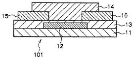
本発明の有機半導体装置101は、図1に示すように、少なくとも基板11、ゲート電極12、ゲート絶縁層13、有機半導体層14、ドレイン電極15及びソース電極16で構成される。この有機半導体装置101は、有機半導体層14が、上述した本発明の有機半導体構造物を構成する有機半導体材料で形成されている。
(Organic semiconductor device)
As shown in FIG. 1, the
構成の一例としては、基板11上に、ゲート電極12、ゲート絶縁層13、配向した有機半導体層14、ドレイン電極15とソース電極16、保護膜17の順に構成される逆スタガー構造、又は、基板11上に、ゲート電極12、ゲート絶縁層13、ドレイン電極15とソース電極16、有機半導体層14、保護膜(図示しない。)の順に構成されるコプラナー構造、を挙げることができる。こうした構成からなる有機半導体装置101は、ゲート電極12に印加される電圧の極性に応じて、蓄積状態又は空乏状態の何れかで動作する。以下、有機半導体装置の構成部材について詳細に説明する。
As an example of the configuration, an inverted stagger structure in which a
(基板)
基板11は、絶縁性の材料であれば広い範囲の材料から選択することができる。例えば、ガラス、アルミナ焼結体などの無機材料、ポリイミド膜、ポリエステル膜、ポリエチレン膜、ポリフェニレンスルフィド膜、ポリパラキシレン膜等の各種の絶縁性材料を挙げることができる。特に、高分子化合物からなる膜を用いると、軽量でフレシキブルな有機半導体装置を作製することができるので、極めて有用である。なお、本発明で適用される基板11の厚さは、25μm〜1.5mm程度である。
(substrate)
The substrate 11 can be selected from a wide range of materials as long as it is an insulating material. Examples thereof include various insulating materials such as glass, an inorganic material such as an alumina sintered body, a polyimide film, a polyester film, a polyethylene film, a polyphenylene sulfide film, and a polyparaxylene film. In particular, the use of a film made of a polymer compound is extremely useful because a lightweight and flexible organic semiconductor device can be manufactured. In addition, the thickness of the board | substrate 11 applied by this invention is about 25 micrometers-1.5 mm.
(ゲート電極)
ゲート電極12は、ポリアニリン、ポリチオフェン等の有機材料からなる電極又は導電性インキを塗布して形成した電極であることが好ましい。これらの電極は、有機材料や導電性インキを塗布して形成できるので、電極形成プロセスが極めて簡便となるという利点がある。塗布法の具体的な手法としては、スピンコート法、キャスト法、引き上げ法、転写法、インクジェット法等が挙げられる。
(Gate electrode)
The
なお、電極として金属膜を形成する場合には、既存の真空成膜法を用いることができ、具体的には、マスク成膜法又はフォトリソグラフ法を用いることができる。この場合には、金、白金、クロム、パラジウム、アルミニウム、インジウム、モリブデン、ニッケル等の金属、これら金属を用いた合金、ポリシリコン、アモルファスシリコン、錫酸化物、酸化インジウム、インジウム・錫酸化物(ITO)等の無機材料を、電極形成用の材料として挙げることができる。また、これらの材料を2種以上併用してもよい。 Note that when a metal film is formed as an electrode, an existing vacuum film formation method can be used, and specifically, a mask film formation method or a photolithographic method can be used. In this case, metals such as gold, platinum, chromium, palladium, aluminum, indium, molybdenum, nickel, alloys using these metals, polysilicon, amorphous silicon, tin oxide, indium oxide, indium / tin oxide ( An inorganic material such as ITO) can be cited as a material for forming an electrode. Two or more of these materials may be used in combination.
ゲート電極の膜厚は、その材質の導電率によるが、50〜1000nm程度であることが好ましい。ゲート電極の厚さの下限は、電極材料の導電率及び下地基板との密着強度によって異なる。ゲート電極の厚さの上限は、後述のゲート絶縁層及びソース・ドレイン電極対を設けた際に、下地基板とゲート電極の段差部分におけるゲート絶縁層による絶縁被覆が十分で、かつその上に形成する電極パターンに断線を生ぜしめないことが必要である。特に、可とう性がある基板を使用した場合には、応力のバランスを考慮する必要がある。 The thickness of the gate electrode depends on the conductivity of the material, but is preferably about 50 to 1000 nm. The lower limit of the thickness of the gate electrode varies depending on the conductivity of the electrode material and the adhesion strength with the base substrate. The upper limit of the thickness of the gate electrode is that when a gate insulating layer and a source / drain electrode pair, which will be described later, are provided, the insulating coating by the gate insulating layer at the stepped portion of the base substrate and the gate electrode is sufficient and formed thereon It is necessary not to cause disconnection in the electrode pattern. In particular, when a flexible substrate is used, it is necessary to consider the balance of stress.
(ゲート絶縁層)
ゲート絶縁層13は、上記のゲート電極12と同じように、有機材料を塗布して形成したものであることが好ましく、使用される有機材料としては、ポリクロロピレン、ポリエチレンテレフタレート、ポリオキシメチレン、ポリビニルクロライド、ポリフッ化ビニリデン、シアノエチルプルラン、ポリメチルメタクリレート、ポリサルフォン、ポリカーボネート、ポリイミド等を挙げることができる。塗布法の具体的な手法としては、スピンコート法、キャスト法、引き上げ法、転写法、インクジェット法等が挙げられる。なお、CVD法等の既存パターンプロセスを用いて形成してもよく、その場合には、SiO2、SiNx、A12O3等の無機材料が好ましく使用される。また、これらの材料を2種以上併用してもよい。
(Gate insulation layer)
The
有機半導体装置の移動度は電界強度に依存するので、ゲート絶縁層の膜厚は、50〜300nm程度であることが好ましい。このときの絶縁耐圧は、2MV/cm以上であることが望ましい。 Since the mobility of the organic semiconductor device depends on the electric field strength, the thickness of the gate insulating layer is preferably about 50 to 300 nm. In this case, the withstand voltage is preferably 2 MV / cm or more.
(ドレイン電極及びソース電極)
ドレイン電極15及びソース電極16は、仕事関数の大きい金属で形成されることが好ましい。その理由としては、後述する液晶性有機半導体材料は、電荷を輸送するキャリアがホールであることから、有機半導体層14とオーミック接触していることが必要となるからである。ここでいう仕事関数とは、固体中の電子を外部に取り出すのに必要な電位差であり、真空準位とフェルミ準位とのエネルギー差として定義される。好ましい仕事関数としては、4.6〜5.2eV程度であり、具体的には、金、白金、透明導電膜(インジウム・スズ酸化物、インジウム・亜鉛酸化物等)等が挙げられる。透明導電膜は、スパッタリング法、電子ビーム(EB)蒸着法で形成することができる。
(Drain electrode and source electrode)
The
なお、本発明で適用されるドレイン電極15及びソース電極16の厚さは、50〜100nm程度である。
The thickness of the
(有機半導体層)
有機半導体層14は、上述した本発明の有機半導体材料により形成された層である。形成される有機半導体層14は、少なくとも常温を含む広い温度範囲において液晶相を呈し、欠陥のない均一な大面積の有機半導体層を形成することができるという特徴的な効果がある。また、有機半導体層14の奏する電荷輸送速度は10−1cm2/V・s以上となる。有機半導体層14がこうした高い電荷輸送速度を有することにより、例えば有機薄膜トランジスタの駆動電圧の低減に寄与したり、応答速度の向上に寄与できるという利点がある。
(Organic semiconductor layer)
The
なお、有機半導体材料を形成する被形成面がゲート絶縁層又は基板である場合には、そのゲート絶縁層又は基板をラビング処理することにより、配向処理膜と、ゲート絶縁層又は基板とを一体のものとすることができる。 Note that when the formation surface on which the organic semiconductor material is formed is a gate insulating layer or a substrate, the alignment processing film and the gate insulating layer or the substrate are integrated with each other by rubbing the gate insulating layer or the substrate. Can be.
(層間絶縁層)
有機半導体装置101には、層間絶縁層を設けることが望ましい。層間絶縁層は、ゲート絶縁層13上にドレイン電極15及びソース電極16を形成する際に、ゲート電極12の表面の汚染を防ぐことを目的として形成される。したがって、層間絶縁層は、ドレイン電極15及びソース電極16を形成する前にゲート絶縁層13の上に形成される。そして、ソース電極15及びドレイン電極16が形成された後においては、チャネル領域上方に位置する部分を完全に除去又は一部を除去するように加工される。除去される層間絶縁層領域は、ゲート電極12のサイズと同等であることが望ましい。
(Interlayer insulation layer)
The
材料としては、SiO2、SiNx、Al2O3等の無機材料や、ポリクロロピレン、ポリエチレンテレフタレート、ポリオキシメチレン、ポリビニルクロライド、ポリフッ化ビニリデン、シアノエチルプルラン、ポリメチルメタクリレート、ポリスルホン、ポリカーボネート、ポリイミド等の有機材料が挙げられる。 Materials include inorganic materials such as SiO 2 , SiN x , Al 2 O 3 , polychloropyrene, polyethylene terephthalate, polyoxymethylene, polyvinyl chloride, polyvinylidene fluoride, cyanoethyl pullulan, polymethyl methacrylate, polysulfone, polycarbonate, polyimide, etc. The organic material is mentioned.
(有機半導体装置の他の態様)
本発明の有機半導体装置においては、その構成として、(i)基板/ゲート電極/ゲート絶縁層(液晶配向層を兼ねる。)/ソース・ドレイン電極/液晶性有機半導体層(/保護層)、(ii)基板/ゲート電極/ゲート絶縁層/ソース・ドレイン電極/液晶配向層/液晶性有機半導体層(/保護層)、(iii)基板/ゲート電極/ゲート絶縁層(液晶配向層を兼ねる)/液晶性有機半導体層/ソース・ドレイン電極/(保護層)、(iv)基板/ゲート電極/ゲート絶縁層(液晶配向層を兼ねる)/液晶性有機半導体層/ソース・ドレイン電極がパターニングされた基板(保護層を兼ねる)、(v)基板/ソース・ドレイン電極/液晶性有機半導体層/ゲート絶縁層(液晶配向層を兼ねる)/ゲート電極/基板(保護層を兼ねる)、(vi)基板(配向層を兼ねる)/ソース・ドレイン電極/液晶性有機半導体層/ゲート絶縁層/ゲート電極/基板(保護層を兼ねる)、又は、(vii)基板/ゲート電極/ゲート絶縁層/ソース・ドレイン電極/液晶性有機半導体層/基板(配向層を兼ねる)、とすることもできる。
(Other aspects of organic semiconductor device)
In the organic semiconductor device of the present invention, the configuration includes (i) substrate / gate electrode / gate insulating layer (also serving as a liquid crystal alignment layer) / source / drain electrode / liquid crystalline organic semiconductor layer (/ protective layer), ii) substrate / gate electrode / gate insulating layer / source / drain electrode / liquid crystal alignment layer / liquid crystalline organic semiconductor layer (/ protective layer), (iii) substrate / gate electrode / gate insulating layer (also serving as a liquid crystal alignment layer) / Liquid crystal organic semiconductor layer / source / drain electrode / (protective layer), (iv) substrate / gate electrode / gate insulating layer (also serving as liquid crystal alignment layer) / liquid crystal organic semiconductor layer / source / drain electrode patterned substrate (Also serves as protective layer), (v) substrate / source / drain electrode / liquid crystal organic semiconductor layer / gate insulating layer (also serves as liquid crystal alignment layer) / gate electrode / substrate (also serves as protective layer), (vi) substrate ( Also serves as an alignment layer) Drain / drain electrode / liquid crystalline organic semiconductor layer / gate insulating layer / gate electrode / substrate (also serves as protective layer) or (vii) substrate / gate electrode / gate insulating layer / source / drain electrode / liquid crystalline organic semiconductor layer / Substrate (also serves as an alignment layer).
こうした有機半導体装置においては、本発明の有機半導体材料を用いることによって、塗布方式で有機半導体層を容易に形成することができる。 In such an organic semiconductor device, the organic semiconductor layer can be easily formed by a coating method by using the organic semiconductor material of the present invention.
以下に、本発明についてさらに詳しく説明する。 Hereinafter, the present invention will be described in more detail.
<クォーターチオフェン誘導体の合成> <Synthesis of quarterthiophene derivatives>
(2-propylthiopheneの合成)
先ず、thiophene 10ml(0.125mol, 1.2eq)を三口フラスコに入れ、Ar置換を行なった。これに、THF30mlを加えて撹拌した後、−78℃まで冷却した。これに、2.6molのnBuLi 40ml(0.104mol,1eq)を滴下した。滴下後、1時間撹拌した後、0℃まで温度を戻した。これに3-bromopropane 10.4ml(0.104mol,1eq)を滴下した。滴下後、1時間撹拌した後、室温まで温度を戻し、更に12時間撹拌した。これをジエチルエーテルで抽出し、pH7まで水洗した後、Na2SO4で脱水した。Na2SO4をろ過して除いた後、溶媒を留去した。これをシリカゲルクロマトグラフィーで精製し、目的物である2-propylthiopheneを得た(実際には蒸留。沸点75℃ 15mmHg)。収量約12g、収率約90%。
(Synthesis of 2-propylthiophene)
First, 10 ml (0.125 mol, 1.2 eq) of thiophene was placed in a three-necked flask, and Ar substitution was performed. To this, 30 ml of THF was added and stirred, and then cooled to -78 ° C. To this, 2.6 mol of nBuLi 40 ml (0.104 mol, 1 eq) was added dropwise. After dripping, after stirring for 1 hour, the temperature was returned to 0 ° C. To this, 10.4 ml (0.104 mol, 1 eq) of 3-bromopropane was added dropwise. After dropping, the mixture was stirred for 1 hour, then returned to room temperature, and further stirred for 12 hours. This was extracted with diethyl ether, washed with water to pH 7, and then dehydrated with Na 2 SO 4 . After removing Na 2 SO 4 by filtration, the solvent was distilled off. This was purified by silica gel chromatography to obtain the desired product, 2-propylthiophene (actual distillation, boiling point: 75 ° C., 15 mmHg). Yield about 12g, about 90%.
(1:2-bromo-5-propylthiopheneの合成)
次に、得られた2-propylthiophene 10g(0.079mol, 1eq)を三口フラスコに入れ、Ar置換を行なった。これにTHF100mlを加えて撹拌した後、0℃まで冷却した。これにNBS 15.5g(0.087mol, 1.1eq)を直接加えた。その後、室温に戻し、12時間撹拌した。これに10%炭酸ナトリウム水溶液を20ml加え、ジエチルエーテルで抽出し、pH7まで水洗した後、Na2SO4で脱水した。Na2SO4をろ過して除いた後、溶媒を留去した。これをシリカゲルクロマトグラフィーで精製し、目的物である2-bromo-5-propylthiophene(化学反応式中の1)を得た。収量約14g、収率約85%。
(1: Synthesis of 2-bromo-5-propylthiophene)
Next, 10 g (0.079 mol, 1 eq) of the obtained 2-propylthiophene was placed in a three-necked flask, and Ar substitution was performed. To this, 100 ml of THF was added and stirred, and then cooled to 0 ° C. To this was added 15.5 g (0.087 mol, 1.1 eq) of NBS directly. Then, it returned to room temperature and stirred for 12 hours. To this was added 20 ml of 10% aqueous sodium carbonate solution, extracted with diethyl ether, washed with water to pH 7, and dehydrated with Na 2 SO 4 . After removing Na 2 SO 4 by filtration, the solvent was distilled off. This was purified by silica gel chromatography to obtain the desired product 2-bromo-5-propylthiophene (1 in the chemical reaction formula). Yield about 14g, about 85%.
(2:5-propyl-2,5’-bitiopheneの合成)
次に、得られた2-bromo-5-propylthiophene 12g(0.056mol, 1eq)、Ni(dppp)Cl2 0.08g(0.148mmol, 0.0025eq)を三口フラスコに入れ、Ar置換を行なった。これに、ジエチルエーテル100mlを加えて撹拌した(反応液α)。これとは別の容器で、Mg1.87g(0.077mol, 1.38eq)を三口フラスコに入れ、Ar置換を行なった。これにジエチルエーテル50mlを加え、撹拌した。これに、2-bromothiophene 11.4g(0.07mol,1.25eq)をジエチルエーテル50mlで希釈した溶液を滴下した。滴下後、2時間refluxさせた後、放冷した(反応液β)。0℃に冷却した反応液αに、反応液βを滴下した。滴下後、2時間撹拌した後、12時間 refluxさせた。これを0℃まで冷却し、2N-HCl 70mlを滴下した。滴下後、室温に戻し、2時間撹拌した。これをジエチルエーテルで抽出し、Na2CO3水溶液でpH7まで水洗した後、Na2SO4で脱水した。Na2SO4をろ過して除いた後、溶媒を留去した。これをシリカゲルクロマトグラフィーで精製し、目的物である5-propyl-2,2’-bitiophene (化学反応式中の2)を得た。収量約9g、収率約75%。
(2: Synthesis of 5-propyl-2,5'-bitiophene)
Next, 12 g (0.056 mol, 1 eq) of 2-bromo-5-propylthiophene and 0.08 g (0.148 mmol, 0.0025 eq) of Ni (dppp) Cl 2 obtained were put into a three-necked flask, and Ar substitution was performed. To this, 100 ml of diethyl ether was added and stirred (reaction liquid α). In a separate container, Mg 1.87 g (0.077 mol, 1.38 eq) was placed in a three-necked flask and replaced with Ar. To this, 50 ml of diethyl ether was added and stirred. To this was added dropwise a solution obtained by diluting 11.4 g (0.07 mol, 1.25 eq) of 2-bromothiophene with 50 ml of diethyl ether. After dropping, the mixture was refluxed for 2 hours and then allowed to cool (reaction solution β). The reaction solution β was added dropwise to the reaction solution α cooled to 0 ° C. After dropping, the mixture was stirred for 2 hours and then refluxed for 12 hours. This was cooled to 0 ° C., and 70 ml of 2N HCl was added dropwise. After dropping, the temperature was returned to room temperature and stirred for 2 hours. This was extracted with diethyl ether, washed with Na 2 CO 3 aqueous solution to pH 7, and then dehydrated with Na 2 SO 4 . After removing Na 2 SO 4 by filtration, the solvent was distilled off. This was purified by silica gel chromatography to obtain the desired product, 5-propyl-2,2′-bitiophene (2 in the chemical reaction formula). Yield about 9g, Yield about 75%.
(3:5-bromo-5’-propyl-2,2’-bitiopheneの合成)
次に、得られた5-propyl-2,2’-bitiophene 8g(0.038mol, 1eq)を三口フラスコに入れ、Ar置換を行なった。これにTHF 100mlを加えて撹拌した後、0℃まで冷却した。これにNBS 7.4g(0.042mol, 1.1eq)を直接添加した。その後、室温に戻し、12時間撹拌した。これに10%炭酸ナトリウム水溶液を加え、ジエチルエーテルで抽出し、pH7まで水洗した後、Na2SO4で脱水した。Na2SO4をろ過して除いた後、溶媒を留去した。これをシリカゲルクロマトグラフィーで精製し、目的物である5-bromo-5’-propyl-2,2’-bitiophene (化学反応式中の3)を得た。収量約8.8g、収率約80%。
(3: Synthesis of 5-bromo-5'-propyl-2,2'-bitiophene)
Next, 8 g (0.038 mol, 1 eq) of the obtained 5-propyl-2,2′-bitiophene was placed in a three-necked flask and subjected to Ar substitution. To this, 100 ml of THF was added and stirred, and then cooled to 0 ° C. To this was added 7.4 g (0.042 mol, 1.1 eq) NBS directly. Then, it returned to room temperature and stirred for 12 hours. To this was added a 10% aqueous sodium carbonate solution, extracted with diethyl ether, washed with water to pH 7, and dehydrated with Na 2 SO 4 . After removing Na 2 SO 4 by filtration, the solvent was distilled off. This was purified by silica gel chromatography to obtain the desired product, 5-bromo-5′-propyl-2,2′-bitiophene (3 in the chemical reaction formula). Yield about 8.8g, Yield about 80%.
(4:5-propyl-2,2’:5’,2”-terthiopheneの合成)
次に、得られた5-bromo-5’-propyl-2,2’-bitiophene 8g(0.028mol, 1eq) 、Ni(dppp)Cl2 0.04g(0.07mmol, 0.0025eq)を三口フラスコに入れ、Ar置換を行なった。これに、ジエチルエーテル100mlを加えて撹拌した(反応液α)。これとは別の容器で、Mg0.94g(0.0385mol, 1.38eq)を三口フラスコに入れ、Ar置換を行なった。これにジエチルエーテル50mlを加え、撹拌した。これに、2-bromothiophene 5.7g(0.035mol,1.25eq)をジエチルエーテル50mlで希釈した溶液を滴下した。滴下後、2時間refluxさせた後、放冷した(反応液β)。0℃に冷却した反応液αに、反応液βを滴下した。滴下後、2時間撹拌した後、12時間 refluxさせた。これを0℃まで冷却し、2N-HCl 30mlを滴下した。滴下後、室温に戻し、2時間撹拌した。これをクロロホルムで抽出し、Na2CO3水溶液でpH7まで水洗した後、Na2SO4で脱水した。Na2SO4をろ過して除いた後、溶媒を留去した。これをシリカゲルクロマトグラフィーで精製し、目的物である5-propyl-2,2’:5’,2”-terthiophene(化学反応式中の4)を得た。収量約6g、収率約75%。
(4: Synthesis of 5-propyl-2,2 ': 5', 2 "-terthiophene)
Next, the obtained 5-bromo-5′-propyl-2,2′-bitiophene 8 g (0.028 mol, 1 eq) and Ni (dppp) Cl 2 0.04 g (0.07 mmol, 0.0025 eq) were placed in a three-necked flask, Ar substitution was performed. To this, 100 ml of diethyl ether was added and stirred (reaction liquid α). In a separate container, 0.94 g (0.0385 mol, 1.38 eq) of Mg was placed in a three-necked flask, and Ar substitution was performed. To this, 50 ml of diethyl ether was added and stirred. A solution obtained by diluting 5.7 g (0.035 mol, 1.25 eq) of 2-bromothiophene with 50 ml of diethyl ether was added dropwise thereto. After dropping, the mixture was refluxed for 2 hours and then allowed to cool (reaction solution β). The reaction solution β was added dropwise to the reaction solution α cooled to 0 ° C. After dropping, the mixture was stirred for 2 hours and then refluxed for 12 hours. This was cooled to 0 ° C., and 30 ml of 2N HCl was added dropwise. After dropping, the temperature was returned to room temperature and stirred for 2 hours. This was extracted with chloroform, washed with Na 2 CO 3 aqueous solution to pH 7, and then dehydrated with Na 2 SO 4 . After removing Na 2 SO 4 by filtration, the solvent was distilled off. This was purified by silica gel chromatography to obtain the target product 5-propyl-2,2 ′: 5 ′, 2 ″ -terthiophene (4 in the chemical reaction formula). Yield: about 6 g, yield: about 75% .
(5:5-propyl-5”-iode-2,2’:5’,2”-terthiopheneの合成)
次に、得られた5-propyl-2,2’:5’,2”-terthiophene 5g(17mmol, 1eq)を三口フラスコに入れ、Ar置換を行なった。これに、THF 100mlを加えて撹拌した後、−78℃まで冷却した。これに、2.6MのnBuLi 7.8ml(20.4mmol, 1.2eq)を滴下した。滴下後、1時間撹拌した後、0℃まで温度を戻した。これにI2 6.47g(25.5mmol, 1.5eq)を直接添加した。滴下後、1時間撹拌した後、室温まで温度を戻し、更に12時間撹拌した。これをクロロホルムで抽出し、pH7まで水洗した後、Na2SO4で脱水した。Na2SO4をろ過して除いた後、溶媒を留去した。これをシリカゲルクロマトグラフィーで精製し、目的物である5-propyl-5”-iode-2,2’:5’,2”-terthiophene(化学反応式中の5)を得た。収量約6.4g、収率約90%。
(5: Synthesis of 5-propyl-5 "-iode-2,2 ': 5', 2" -terthiophene)
Next, 5 g (17 mmol, 1 eq) of 5-propyl-2,2 ′: 5 ′, 2 ″ -terthiophene obtained was placed in a three-necked flask and subjected to Ar substitution. To this, 100 ml of THF was added and stirred. after, and cooled to -78 ° C.. This, 2.6 M of nBuLi 7.8ml (20.4mmol, 1.2eq) was added dropwise. after the dropwise addition, stirring for 1 hour, 0 ° C. the temperature was returned to. This I 2 6.47 g (25.5 mmol, 1.5 eq) was added directly, and after stirring for 1 hour, the temperature was returned to room temperature, and the mixture was further stirred for 12 hours, extracted with chloroform, washed with water to pH 7, and then Na 2. after removing by filtration .na 2 SO 4 which had been dehydrated by SO 4, the solvent was distilled off. This was purified by silica gel chromatography, the desired product 5-propyl-5 "-iode- 2,2 ' : 5 ', 2 "-terthiophene (5 in the chemical reaction formula) was obtained. Yield: about 6.4 g, about 90%.
(6:5-propyl-2,2’:5’,2”:5”,2”’-quaterthiopheneの合成)
先ず、Mg 0.94g(0.0385mol, 1.9eq)にTHF200mlを加え、攪拌した。そこに2-bromothiophene 5.7g(0.035mol,1.75eq) を滴下し2時間還流した。その後、反応溶液を0℃に冷却し、Ni(dppp)Cl2 0.04g(0.07mmol, 0.0035eq)、5-propyl-5”-iode-2,2’:5’,2”-terthiophene 8.2g(20.0mmol, 1eq)を加え、10時間還流した。その後、これを0℃まで冷却し、2N-HCl 30mlを滴下した。滴下後、室温に戻し、2時間撹拌した。これをクロロホルムで抽出し、Na2CO3水溶液でpH7まで水洗した後、Na2SO4で脱水した。Na2SO4をろ過して除いた後、溶媒を留去した。これをシリカゲルクロマトグラフィーで精製し、目的物である5-propyl-2,2’:5’,2”:5”,2”’-quaterthiophene(化学反応式中の6)を得た。収量約6g、収率約75%。
(6: Synthesis of 5-propyl-2,2 ': 5', 2 ": 5", 2 "'-quaterthiophene)
First, 200 ml of THF was added to 0.94 g (0.0385 mol, 1.9 eq) of Mg and stirred. To this was added dropwise 5.7 g (0.035 mol, 1.75 eq) of 2-bromothiophene and refluxed for 2 hours. Thereafter, the reaction solution was cooled to 0 ° C., and Ni (dppp) Cl 2 0.04 g (0.07 mmol, 0.0035 eq), 5-propyl-5 ”-iode-2,2 ′: 5 ′, 2” -terthiophene 8.2 g (20.0 mmol, 1 eq) was added and refluxed for 10 hours. Thereafter, this was cooled to 0 ° C., and 30 ml of 2N HCl was added dropwise. After dropping, the temperature was returned to room temperature and stirred for 2 hours. This was extracted with chloroform, washed with Na 2 CO 3 aqueous solution to pH 7, and then dehydrated with Na 2 SO 4 . After removing Na 2 SO 4 by filtration, the solvent was distilled off. This was purified by silica gel chromatography to obtain the target product 5-propyl-2,2 ′: 5 ′, 2 ″: 5 ″, 2 ″ ′-quaterthiophene (6 in the chemical reaction formula). 6 g, about 75% yield.
(7:5-propyl-5”’-iode- 2,2’:5’,2”:5”,2”’-quaterthiophene の合成)
次に、得られた5-propyl-2,2’:5’,2”:5”,2”’-quaterthiophene 5g(13.4mmol,1eq)を三口フラスコに入れ、Ar置換を行なった。これに、THF200mlを加えて撹拌した後、−78℃まで冷却した。これに、2.6molのnBuLi 6.2ml(16.1mmol,1.2eq)を滴下した。滴下後、1時間撹拌した後、0℃まで温度を戻した。これにI2 5.1g(20.1mmol,1.5eq)を直接添加した。滴下後、1時間撹拌した後、室温まで温度を戻し、更に12時間撹拌した。これをクロロホルムで抽出し、pH7まで水洗した後、Na2SO4で脱水した。Na2SO4をろ過して除いた後、溶媒を留去した。これをシリカゲルクロマトグラフィーで精製し、目的物である5-propyl-5”’-iode- 2,2’:5’,2”:5”,2”’-quaterthiophene(化学反応式中の7)を得た。収量約5g、収率約76%。
(7: Synthesis of 5-propyl-5 ”'-iode-2,2': 5 ', 2": 5 ", 2"'-quaterthiophene)
Next, 5 g (13.4 mmol, 1 eq) of the obtained 5-propyl-2,2 ′: 5 ′, 2 ″: 5 ″, 2 ″ ′-quaterthiophene was placed in a three-necked flask and subjected to Ar substitution. After adding 200 ml of THF and stirring, the mixture was cooled to −78 ° C. To this was added dropwise 6.2 mol (16.1 mmol, 1.2 eq) of 2.6 mol of nBuLi, and stirred for 1 hour, and then the temperature was raised to 0 ° C. To this, 5.1 g (20.1 mmol, 1.5 eq) of I 2 was directly added, and after stirring for 1 hour, the temperature was returned to room temperature, followed by further stirring for 12 hours, which was extracted with chloroform, pH 7 washed with water until after removed by filtration .na 2 SO 4 was dried over Na 2 SO 4, the solvent was distilled off. This was purified by silica gel chromatography, the desired product 5-propyl-5 "'-iode-2,2': 5 ', 2 ": 5", 2 "'-quaterthiophene (7 in the chemical reaction formula) was obtained. Yield: about 5 g, yield: about 76%.
(8:5-propyl-(5”’-hexyl-1-yne)-2,2’:5’,2”:5”,2”’-quaterthiophene の合成)
次に、得られた5-propyl-5”’-iode- 2,2’:5’,2”:5”,2”’-quaterthiophene 4.5g(9.0mmol,1eq) 、Pd(PPh3)Cl2 0.032g(0.045mmol,0.005eq)、CuI 0.0085g(0.045mmol,0.005eq)を三口フラスコに入れ、Ar置換を行なった。これに、THF200ml、TEA5ml、1-hexyne 1.48g(18mmol,2eq)を加えて、5時間撹拌した。これをジエチルエーテルで抽出し、水洗した後、Na2SO4で脱水した。Na2SO4をろ過して除いた後、溶媒を留去した。これをシリカゲルクロマトグラフィーで精製し、目的物である本発明に係る5-propyl-(5”’-hexyl-1-yne)-2,2’:5’,2”:5”,2”’-quaterthiophene(化学反応式中の8)を得た。収量約2.5g、収率約62%。
(8: Synthesis of 5-propyl- (5 "'-hexyl-1-yne) -2,2': 5 ', 2": 5 ", 2"'-quaterthiophene)
Next, 5-propyl-5 "'-iode-2,2': 5 ', 2": 5 ", 2"'-quaterthiophene 4.5 g (9.0 mmol, 1 eq), Pd (PPh 3 ) Cl 2 0.032 g (0.045 mmol, 0.005 eq) and CuI 0.0085 g (0.045 mmol, 0.005 eq) were placed in a three-necked flask and subjected to Ar substitution. To this, 200 ml of THF, 5 ml of TEA and 1.48 g (18 mmol, 2 eq) of 1-hexyne were added and stirred for 5 hours. This was extracted with diethyl ether, washed with water, and dehydrated with Na 2 SO 4 . After removing Na 2 SO 4 by filtration, the solvent was distilled off. This was purified by silica gel chromatography, and the target product 5-propyl- (5 "'-hexyl-1-yne) -2,2': 5 ', 2": 5 ", 2"' -quaterthiophene (8 in the chemical reaction formula) was obtained. Yield about 2.5 g, about 62% yield.
(NMRデータ)
こうして得られたクォーターチオフェン誘導体である5-propyl-(5”’-hexyl-1-yne)-2,2’:5’,2”:5”,2”’-quaterthiopheneについてのNMRデータは以下のとおりである。
(NMR data)
The NMR data for the thus obtained quarterthiophene derivative 5-propyl- (5 ”'-hexyl-1-yne) -2,2': 5 ', 2": 5 ", 2"'-quaterthiophene are as follows: It is as follows.
δ=0.95(3H,t,J=8.0Hz), 1.02(3H,t,J=8.0Hz), 1.50(2H,m), 1.61(2H,m), 1.69(2H,m), 2.48(2H,t,J=6.7Hz), 2.82(2H,t,9.3Hz), 6.83(1H,d,J=3.7Hz), 6.99(4H,m), 7.0(2H,s), 7.1(1H,d,J=3.2) in CDCl3 δ = 0.95 (3H, t, J = 8.0Hz), 1.02 (3H, t, J = 8.0Hz), 1.50 (2H, m), 1.61 (2H, m), 1.69 (2H, m), 2.48 (2H , t, J = 6.7Hz), 2.82 (2H, t, 9.3Hz), 6.83 (1H, d, J = 3.7Hz), 6.99 (4H, m), 7.0 (2H, s), 7.1 (1H, d , J = 3.2) in CDCl 3
<相系列>
得られたクォーターチオフェン誘導体である5-propyl-(5”’-hexyl-1-yne)-2,2’:5’,2”:5”,2”’-quaterthiophene(化学反応式中の8)は、DSC測定によれば、昇温過程においては約210.2℃で吸熱ピークが見られ、降温過程においては約208.7℃で発熱ピークが見られた。得られたクォーターチオフェン誘導体を注入したガラスセルを使って偏光顕微鏡によるテクスチャー観察を行なったところ、昇温過程で吸熱ピークを示した210℃前後で液晶相から等方相に相転移するのが確認され、降温過程で発熱ピークを示した209℃前後で等方相から液晶相に相転移した。また、液晶相から結晶相への相転移は、−120℃まで起こらなかった。なお、このクォーターチオフェン誘導体について、X線回折測定を行ったところ、少なくとも常温において、スメクティック相特有の長距離秩序を示すことが確認された。
<Phase series>
The obtained quarterthiophene derivative 5-propyl- (5 ”'-hexyl-1-yne) -2,2': 5 ', 2": 5 ", 2"'-quaterthiophene (8 in the chemical reaction formula) According to DSC measurement, an endothermic peak was observed at about 210.2 ° C. during the temperature rising process, and an exothermic peak was observed at about 208.7 ° C. during the temperature lowering process. Using a glass cell into which the obtained quarterthiophene derivative was injected, the texture was observed with a polarizing microscope, and it was confirmed that the phase transition from the liquid crystal phase to the isotropic phase occurred around 210 ° C, which showed an endothermic peak during the temperature rising process. The phase transition from the isotropic phase to the liquid crystal phase occurred around 209 ° C., which showed an exothermic peak in the temperature lowering process. Further, the phase transition from the liquid crystal phase to the crystal phase did not occur up to -120 ° C. When this quarter thiophene derivative was subjected to X-ray diffraction measurement, it was confirmed that it exhibited a long-range order peculiar to a smectic phase at least at room temperature.
<電荷移動度測定>
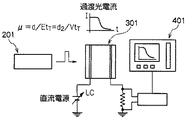
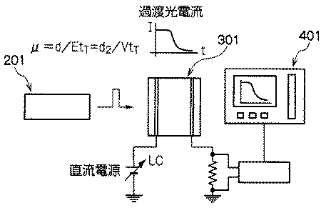
得られたクォーターチオフェン誘導体である5-propyl-(5”’-hexyl-1-yne)-2,2’:5’,2”:5”,2”’-quaterthiophene(化学反応式中の8)を、ITO(インジウム錫オキサイド)電極付きガラスセルに注入し、ホットプレート上で図2に示す装置を用いた過渡光電流測定(TOF法)により電荷移動度を測定した。このクォーターチオフェン誘導体は常温でスメクティック相を示しており、正孔電荷移動度は常温で1×10⁻¹cm2/V・sであった。なお、過渡光電流測定は、本実施例では波長337nmのN2パルスレーザーにより試料を励起する方法を用いた。図2中、符号201はN2パルスレーザーであり、符号301は試料であり、符号401はデジタルオシロスコープである。
<Charge mobility measurement>
The obtained quarterthiophene derivative 5-propyl- (5 ”'-hexyl-1-yne) -2,2': 5 ', 2": 5 ", 2"'-quaterthiophene (8 in the chemical reaction formula) ) Was injected into a glass cell with an ITO (indium tin oxide) electrode, and the charge mobility was measured by transient photocurrent measurement (TOF method) using the apparatus shown in FIG. 2 on a hot plate. This quarter thiophene derivative showed a smectic phase at room temperature, and the hole charge mobility was 1 × 10 −1 cm 2 / V · s at room temperature. In the present embodiment, the transient photocurrent measurement was performed by exciting the sample with an N 2 pulse laser having a wavelength of 337 nm. In FIG. 2,
従来の液晶性有機半導体材料では常温を含む温度範囲で高い電荷移動度を示すものは少ないが、本発明に係るクォーターチオフェン誘導体は、常温を含む温度範囲で1×10⁻¹cm2/V・s程度の高い電荷移動度を示すことが確認された。 Although few conventional liquid crystalline organic semiconductor materials exhibit high charge mobility in a temperature range including normal temperature, the quarter thiophene derivative according to the present invention has a temperature range including normal temperature of 1 × 10 −1 cm 2 / V · It was confirmed that the charge mobility was as high as about s.
以上説明したように、本発明に係るクォーターチオフェン誘導体は、少なくとも−40〜+90℃の使用温度範囲で高次の凝集状態をとる液晶相を示し、しかも、高速電荷輸送も確認できた。本発明に係るクォーターチオフェン誘導体を有機トランジスタへ応用した際には、従来のチオフェン骨格材料と同等以上の特性を示すのみならず、液晶性由来の結晶粒界による電荷輸送能の劣化が室温を含む広い温度範囲で起こり難いという点で優れている。 As described above, the quarter thiophene derivative according to the present invention exhibits a liquid crystal phase that takes a high-order aggregation state in a use temperature range of at least −40 to + 90 ° C., and has also confirmed high-speed charge transport. When the quarter thiophene derivative according to the present invention is applied to an organic transistor, it not only exhibits a property equal to or better than that of a conventional thiophene skeleton material, but also includes a deterioration in charge transport capability due to crystal grain boundaries derived from liquid crystallinity. It is excellent in that it hardly occurs in a wide temperature range.
101 有機半導体装置
11 基板
12 ゲート電極
13 ゲート絶縁層
14 高分子有機半導体層
15 ドレイン電極
16 ソース電極
201 N2パルスレーザー
301 試料
401 デジタルオシロスコープ
Claims (6)
Use of the organic semiconductor structure according to any one of claims 3 to 5 as an organic transistor, an organic EL element, an organic electronic device, or an organic solar battery.
Priority Applications (2)
| Application Number | Priority Date | Filing Date | Title |
|---|---|---|---|
| JP2004108528A JP4668544B2 (en) | 2004-03-31 | 2004-03-31 | Organic semiconductor material, organic semiconductor structure and organic semiconductor device |
| US11/092,238 US7405003B2 (en) | 2004-03-31 | 2005-03-29 | Organic semiconductor material, organic semiconductor structure, and organic semiconductor device |
Applications Claiming Priority (1)
| Application Number | Priority Date | Filing Date | Title |
|---|---|---|---|
| JP2004108528A JP4668544B2 (en) | 2004-03-31 | 2004-03-31 | Organic semiconductor material, organic semiconductor structure and organic semiconductor device |
Publications (2)
| Publication Number | Publication Date |
|---|---|
| JP2005294588A true JP2005294588A (en) | 2005-10-20 |
| JP4668544B2 JP4668544B2 (en) | 2011-04-13 |
Family
ID=35327171
Family Applications (1)
| Application Number | Title | Priority Date | Filing Date |
|---|---|---|---|
| JP2004108528A Expired - Fee Related JP4668544B2 (en) | 2004-03-31 | 2004-03-31 | Organic semiconductor material, organic semiconductor structure and organic semiconductor device |
Country Status (2)
| Country | Link |
|---|---|
| US (1) | US7405003B2 (en) |
| JP (1) | JP4668544B2 (en) |
Families Citing this family (6)
| Publication number | Priority date | Publication date | Assignee | Title |
|---|---|---|---|---|
| WO2003067667A1 (en) * | 2002-02-08 | 2003-08-14 | Dai Nippon Printing Co., Ltd. | Organic semiconductor structure, process for producing the same, and organic semiconductor device |
| JPWO2006064776A1 (en) * | 2004-12-17 | 2008-06-12 | コニカミノルタホールディングス株式会社 | Method for producing organic thin film transistor |
| GB2424759A (en) * | 2005-04-01 | 2006-10-04 | Seiko Epson Corp | Inkjet deposition of polythiophene semiconductor material dissolved in halogenated aromatic solvents |
| KR20060116534A (en) * | 2005-05-10 | 2006-11-15 | 삼성에스디아이 주식회사 | Thin film transistor, method for manufacturing same, and flat panel display device having same |
| US8138075B1 (en) | 2006-02-06 | 2012-03-20 | Eberlein Dietmar C | Systems and methods for the manufacture of flat panel devices |
| JP5071921B2 (en) * | 2006-06-08 | 2012-11-14 | 独立行政法人産業技術総合研究所 | Smectic liquid crystal compounds |
Citations (3)
| Publication number | Priority date | Publication date | Assignee | Title |
|---|---|---|---|---|
| JPH10312711A (en) * | 1997-03-10 | 1998-11-24 | Dainippon Printing Co Ltd | Liquid crystalline charge transport material |
| JP2003283005A (en) * | 2002-03-26 | 2003-10-03 | Dainippon Printing Co Ltd | Organic semiconductor, light emitting element and light receiving element using the same |
| EP1398336A1 (en) * | 2002-09-14 | 2004-03-17 | MERCK PATENT GmbH | Mono-, Oligo- and Poly(3-alkynylthiophenes) and their Use as Charge Transport Materials |
Family Cites Families (1)
| Publication number | Priority date | Publication date | Assignee | Title |
|---|---|---|---|---|
| KR100248392B1 (en) * | 1997-05-15 | 2000-09-01 | 정선종 | Organic Active Driving Electroluminescent Device Combined with Organic Field Effect Transistor and Fabrication Method |
-
2004
- 2004-03-31 JP JP2004108528A patent/JP4668544B2/en not_active Expired - Fee Related
-
2005
- 2005-03-29 US US11/092,238 patent/US7405003B2/en not_active Expired - Fee Related
Patent Citations (3)
| Publication number | Priority date | Publication date | Assignee | Title |
|---|---|---|---|---|
| JPH10312711A (en) * | 1997-03-10 | 1998-11-24 | Dainippon Printing Co Ltd | Liquid crystalline charge transport material |
| JP2003283005A (en) * | 2002-03-26 | 2003-10-03 | Dainippon Printing Co Ltd | Organic semiconductor, light emitting element and light receiving element using the same |
| EP1398336A1 (en) * | 2002-09-14 | 2004-03-17 | MERCK PATENT GmbH | Mono-, Oligo- and Poly(3-alkynylthiophenes) and their Use as Charge Transport Materials |
Also Published As
| Publication number | Publication date |
|---|---|
| JP4668544B2 (en) | 2011-04-13 |
| US20060076554A1 (en) | 2006-04-13 |
| US7405003B2 (en) | 2008-07-29 |
Similar Documents
| Publication | Publication Date | Title |
|---|---|---|
| US10937964B2 (en) | Organic semiconductor material | |
| TWI535726B (en) | Benzothiophene benzothiophene derivatives, organic semiconductor materials and organic transistors | |
| KR101429370B1 (en) | Organic semiconductor material, organic semiconductor thin film, and organic thin film transistor | |
| JP4820287B2 (en) | Polyacene compounds and organic semiconductor thin films | |
| JPWO2012005310A1 (en) | Fluorine-containing aromatic compounds, organic semiconductor materials, and organic thin film devices | |
| JP6170488B2 (en) | Novel condensed polycyclic aromatic compounds and uses thereof | |
| TWI605050B (en) | Organic thin film transistor, naphthobisthiazine compound and usage thereof | |
| TW201641503A (en) | Organic compound, organic semiconductor material, organic thin film and its manufacturing method, organic semiconductor composition, and organic semiconductor device | |
| US7935828B2 (en) | Organic semiconductor material, organic semiconductor structure and organic semiconductor apparatus | |
| JP2006206503A (en) | PI electron compound and n-type organic field effect transistor using the same | |
| JP4668544B2 (en) | Organic semiconductor material, organic semiconductor structure and organic semiconductor device | |
| TW201443060A (en) | Novel condensed polycyclic aromatic compounds and uses thereof | |
| JPWO2015133471A1 (en) | Compound, polymer obtained by polymerizing the compound, organic semiconductor material and use thereof | |
| US11038116B2 (en) | Compound and organic thin film and thin film transistor and electronic device | |
| JP6247568B2 (en) | Organic thin-film transistors, organic semiconductor materials for non-emissive organic semiconductor devices and their applications | |
| JP5228411B2 (en) | [1] Benzochalcogeno [3,2-b] [1] Compound having benzochalcogenophene skeleton and organic transistor using the same | |
| US8480926B2 (en) | Liquid-crystalline compound and organic semiconductor device containing the compound | |
| JP5964703B2 (en) | Organic semiconductor material and organic transistor | |
| JP5252508B2 (en) | ORGANIC SEMICONDUCTOR MATERIAL, ITS MANUFACTURING METHOD, AND USE OF ORGANIC SEMICONDUCTOR MATERIAL | |
| TW201529580A (en) | Novel condensed polycyclic aromatic compounds and uses thereof | |
| US20240334816A1 (en) | Hole transport material, and photoelectric conversion element and organic solar cell using hole transport material | |
| US20070045613A1 (en) | Organic semiconductor material, Organic semiconductor structure and Organic semiconductor apparatus | |
| JP5952576B2 (en) | Liquid crystalline styryl derivative having excellent solubility, method for producing the same, conductive liquid crystal material, and organic semiconductor element | |
| JP2021044546A (en) | Organic semiconductor materials and organic thin film transistors | |
| JP2013058674A (en) | Organic semiconductor material and organic semiconductor device comprising the same |
Legal Events
| Date | Code | Title | Description |
|---|---|---|---|
| A621 | Written request for application examination |
Free format text: JAPANESE INTERMEDIATE CODE: A621 Effective date: 20070123 |
|
| TRDD | Decision of grant or rejection written | ||
| A01 | Written decision to grant a patent or to grant a registration (utility model) |
Free format text: JAPANESE INTERMEDIATE CODE: A01 Effective date: 20101228 |
|
| A01 | Written decision to grant a patent or to grant a registration (utility model) |
Free format text: JAPANESE INTERMEDIATE CODE: A01 |
|
| A61 | First payment of annual fees (during grant procedure) |
Free format text: JAPANESE INTERMEDIATE CODE: A61 Effective date: 20110113 |
|
| FPAY | Renewal fee payment (event date is renewal date of database) |
Free format text: PAYMENT UNTIL: 20140121 Year of fee payment: 3 |
|
| R150 | Certificate of patent or registration of utility model |
Free format text: JAPANESE INTERMEDIATE CODE: R150 |
|
| LAPS | Cancellation because of no payment of annual fees |