JP2005294529A - Electronic component manufacturing method and electronic device - Google Patents
Electronic component manufacturing method and electronic device Download PDFInfo
- Publication number
- JP2005294529A JP2005294529A JP2004107505A JP2004107505A JP2005294529A JP 2005294529 A JP2005294529 A JP 2005294529A JP 2004107505 A JP2004107505 A JP 2004107505A JP 2004107505 A JP2004107505 A JP 2004107505A JP 2005294529 A JP2005294529 A JP 2005294529A
- Authority
- JP
- Japan
- Prior art keywords
- resin
- substrate
- recess
- frame member
- electronic component
- Prior art date
- Legal status (The legal status is an assumption and is not a legal conclusion. Google has not performed a legal analysis and makes no representation as to the accuracy of the status listed.)
- Pending
Links
Images


Classifications
-
- H10W72/0198—
Landscapes
- Structures Or Materials For Encapsulating Or Coating Semiconductor Devices Or Solid State Devices (AREA)
- Encapsulation Of And Coatings For Semiconductor Or Solid State Devices (AREA)
Abstract
【課題】 枠部材を用いて回路素子を被覆する樹脂層を形成する際に、樹脂が枠部材の外側に溢流することを防ぎ、樹脂で被覆される回路素子を含む電子部品を歩留良く製造することのできる電子部品の製造方法を提供する。
【解決手段】 基板11の回路素子を含むチップ12が実装された表面にチップ12を囲むように枠部材を設けるに際し、枠部材として、凹所13に臨む壁部1bに交わり、かつ基板11に接しない面1aの摩擦抵抗が、基板11のチップ12が実装される表面の摩擦抵抗よりも大きくなるように形成される枠部材1を設ける。また、凹所13に臨む壁部1bに交わり、かつ基板11に接しない面1aに、凹所13に供給されるべき封止樹脂14を溜め得る樹脂溜り部を設ける。また、基板11のチップ12が設けられる表面から遠ざかるにつれて凹所13の平面積が大きくなるように、凹所13に臨む壁部1bの厚み方向に段差部を設ける。
【選択図】 図1A
PROBLEM TO BE SOLVED: To prevent a resin from overflowing to the outside of a frame member when forming a resin layer covering a circuit element using a frame member, and to obtain an electronic component including a circuit element coated with the resin with a high yield. A method of manufacturing an electronic component that can be manufactured is provided.
When a frame member is provided so as to surround a chip 12 on a surface on which a chip 12 including circuit elements of the substrate 11 is mounted, the frame member intersects a wall portion 1b facing a recess 13 as a frame member and The frame member 1 is provided so that the frictional resistance of the non-contact surface 1a is larger than the frictional resistance of the surface on which the chip 12 of the substrate 11 is mounted. In addition, a resin reservoir that can store the sealing resin 14 to be supplied to the recess 13 is provided on the surface 1 a that intersects the wall 1 b facing the recess 13 and does not contact the substrate 11. Further, a stepped portion is provided in the thickness direction of the wall portion 1b facing the recess 13 so that the flat area of the recess 13 increases as the distance from the surface on which the chip 12 of the substrate 11 is provided.
[Selection] Figure 1A
Description
本発明は、樹脂で被覆される回路素子を含む電子部品の製造に用いられる電子部品の製造方法、および該製造方法によって製造される電子部品を搭載する電子機器に関する。 The present invention relates to a manufacturing method of an electronic component used for manufacturing an electronic component including a circuit element coated with a resin, and an electronic device on which the electronic component manufactured by the manufacturing method is mounted.
光ピックアップ装置などの電子機器に搭載される電子部品は、外部環境から回路素子を保護することなどを目的として、基板表面に実装される回路素子を樹脂層などのパッケージで被覆した状態で使用される。このような樹脂で被覆される回路素子を含む電子部品は、たとえば以下のようにして製造される(たとえば、特許文献1参照)。 Electronic components mounted on electronic devices such as optical pickup devices are used with circuit elements mounted on the substrate surface covered with a package such as a resin layer for the purpose of protecting the circuit elements from the external environment. The An electronic component including a circuit element covered with such a resin is manufactured, for example, as follows (see, for example, Patent Document 1).
図7は、従来技術による電子部品の製造における各工程の状態を模式的に示す斜視図である。図7A(a)は、樹脂成形用型枠61を基板63に配設する様子を示す図であり、図7A(b)は、樹脂成形用型枠61を基板63に配設した状態を示す図である。まず、配線が形成された基板63の表面の所定の位置に、回路素子が形成された複数のチップ62を実装する。基板63のチップ62が実装される表面の反対側の表面(以下、基板63の裏面と称する)には、電子部品の端子電極となる図示しない電極が形成されている。次いで、基板63のチップ62が実装された表面の所定の位置に、樹脂成形用型枠61(以下、単に型枠61とも称する)を設ける。これによって、基板63のチップ62が実装される表面を底部とし、型枠61の側面部を壁部とする凹所60が形成される。
FIG. 7 is a perspective view schematically showing the state of each step in the production of an electronic component according to the prior art. FIG. 7A (a) is a diagram showing a state where the
型枠61としては、シリコーンゴムなどのシート材に、樹脂などからなるシート状の基材の両面に粘着剤層が形成された両面粘着シートを貼り合わせてなるラミネートシート材を、矩形状の開口部61aを有するように加工したものなどが用いられる。ラミネートシート材からなる型枠61は、治具などを使用して基板63の表面に貼り付けられる。
As the
図7B(c)は、凹所60に封止樹脂64を充填した状態を示す図である。型枠61と基板63のチップ62が実装される表面とによって形成される凹所60に、樹脂充填装置などによって液状の封止樹脂64を供給して充填する。次いで、凹所60に封止樹脂64が充填された基板63をオーブンに搬送し、オーブンでキュア(加熱)して封止樹脂64を硬化させる。これによって、チップ62を被覆する樹脂層65が形成される。
FIG. 7B (c) is a view showing a state in which the
図7B(d)は、樹脂成形用型枠61を基板63の表面から剥離した状態を示す図であり、図7C(e)は、基板63および樹脂層65を切断する様子を示す図である。封止樹脂64を硬化して樹脂層65を形成した後、型枠61を基板63の表面から剥離する。次いで、基板63および樹脂層65を、基板63の表面に設けられる複数のチップ62が1個ずつ含まれるように、ダイシングマシンなどで所定の切断線67に沿って切断し、個々の電子部品66に分割する。以上のようにして、樹脂で被覆される回路素子を含む電子部品66が製造される。
FIG. 7B (d) is a view showing a state where the
従来技術には、以下のような問題点がある。図7B(c)に示す工程において、型枠61と基板63のチップ62が実装される表面とによって形成される凹所60に充填される封止樹脂64は、オーブンでのキュアによって硬化されるまでの間は流動性を有する状態にある。このため、樹脂充填時、オーブンへの搬送時などに基板63の傾き、揺れなどが生じると、凹所60から封止樹脂64が型枠61の外側に溢流しやすい。特に、オーブンによる硬化時の高温状態では、封止樹脂64の粘度が低下して流動性が高くなるので、基板63の傾きなどによる封止樹脂64の溢流が一層発生しやすくなる。
The prior art has the following problems. In the step shown in FIG. 7B (c), the
基板63の裏面には電子部品の端子電極となる電極などが設けられるので、前述のように封止樹脂64が型枠61の外側に溢流し、基板63の裏面に付着すると、端子電極などが絶縁性の封止樹脂64で汚染されて機能しなくなり、歩留が低下するという問題が生じる。
Since an electrode to be a terminal electrode of an electronic component is provided on the back surface of the
また、型枠61の外側に溢流した封止樹脂64によって樹脂供給装置などの動作が阻害され、生産性が低下するという問題もある。特に、封止樹脂64を型枠61の高さ一杯まで充填する場合には、封止樹脂64が型枠61から溢れ出やすく、樹脂充填装置に悪影響を与え、生産能力の低下を引起しやすい。
Further, the
前述の図7B(c)に示す工程において凹所60に充填される封止樹脂64は、オーブンなどによるキュア中に蒸発し、凹所60に充填された量よりも減少する。このため、所望の厚みの樹脂層65を形成するのに必要な量と同じ量の封止樹脂64を凹所60に充填した場合、硬化後に形成される樹脂層65の厚みは所望の値すなわち設計値よりも小さくなる。このように樹脂層65の厚みが設計値よりも小さくなると、電子部品の不良が発生しやすくなり、歩留が低下するという問題が生じる。たとえば、光ピックアップ装置に備わる電子部品のようにチップ62の表面に受光素子を備え、パッケージの上部すなわち樹脂層65の表面が受光面となる電子部品を製造する場合には、光路長の設計値からのずれが生じ、光学特性の不良が発生しやすくなる。特に最近では、電子部品の薄型化および小型化に伴い、樹脂層65の厚みの設計値からのずれによる電子部品の不良が発生しやすくなっており、樹脂層65の厚みの減少を抑えることが強く求められている。
The
したがって、型枠61に封止樹脂64を充填する際には、キュア中に封止樹脂64が蒸発することを考慮し、所望の厚みの樹脂層65を構成する封止樹脂64の量よりもやや多めになるように、封止樹脂64を型枠61の高さ一杯まで充填する必要がある。しかしながら、特許文献1などに記載の電子部品の製造方法において、封止樹脂64を型枠61の高さ一杯まで充填しようとすると、前述のように封止樹脂64が型枠61から溢れ出し、樹脂充填装置の生産能力の低下を招きやすい。
Therefore, when the
本発明の目的は、基板表面に設けられる回路素子を被覆する樹脂層を、基板表面と型枠とによって形成される凹所に樹脂を充填して形成する際に、樹脂が型枠の外側に溢流することを防ぎ、樹脂で被覆される回路素子を含む電子部品を歩留良く製造することのできる電子部品の製造方法、および該製造方法によって製造される電子部品を搭載する電子機器を提供することである。 An object of the present invention is to form a resin layer covering a circuit element provided on a substrate surface by filling the resin formed in a recess formed by the substrate surface and the mold with the resin outside the mold. Provided is an electronic component manufacturing method capable of manufacturing an electronic component including a circuit element coated with a resin with good yield, and an electronic device on which the electronic component manufactured by the manufacturing method is mounted. It is to be.
本発明は、基板の一表面に回路素子を設ける素子配設工程と、基板の回路素子が設けられる表面に回路素子を被覆するように樹脂を供給する樹脂供給工程と、基板の前記表面に供給される樹脂を硬化させる樹脂硬化工程とを含み、樹脂で被覆される回路素子を含む電子部品を製造する電子部品の製造方法であって、
樹脂供給工程では、
基板の回路素子が設けられる表面に、基板の前記表面を底部として樹脂を供給すべき凹所を形成し得る枠部材であって、前記凹所に臨む壁部に交わり、かつ基板に接しない面の摩擦抵抗が、基板の回路素子が設けられる表面の摩擦抵抗よりも大きくなるように形成される枠部材を、回路素子を囲むように設け、
枠部材と基板の前記表面とによって形成される凹所に樹脂を供給することを特徴とする電子部品の製造方法である。
The present invention provides an element disposing step of providing a circuit element on one surface of a substrate, a resin supplying step of supplying a resin so as to cover the circuit element on the surface of the substrate on which the circuit element is provided, and supplying the surface to the surface of the substrate A method of manufacturing an electronic component, including a resin curing step of curing the resin to be manufactured, and manufacturing an electronic component including a circuit element coated with the resin,
In the resin supply process,
A frame member capable of forming a recess to which resin should be supplied with the surface of the substrate as a bottom portion on a surface on which a circuit element of the substrate is provided, and is a surface that intersects with a wall facing the recess and does not contact the substrate A frame member formed so that the frictional resistance of the substrate is larger than the frictional resistance of the surface on which the circuit element of the substrate is provided is provided so as to surround the circuit element,
A method of manufacturing an electronic component comprising supplying resin into a recess formed by a frame member and the surface of a substrate.
また本発明は、枠部材の前記凹所に臨む壁部に交わり、かつ基板に接しない面の十点平均粗さRzが、1μm以上、5μm以下であることを特徴とする。 Further, the present invention is characterized in that the ten-point average roughness Rz of the surface that intersects the wall portion facing the recess of the frame member and does not contact the substrate is 1 μm or more and 5 μm or less.
また本発明は、基板の一表面に回路素子を設ける素子配設工程と、基板の回路素子が設けられる表面に回路素子を被覆するように樹脂を供給する樹脂供給工程と、基板の前記表面に供給される樹脂を硬化させる樹脂硬化工程とを含み、樹脂で被覆される回路素子を含む電子部品を製造する電子部品の製造方法であって、
樹脂供給工程では、
基板の回路素子が設けられる表面に、基板の前記表面を底部として樹脂を供給すべき凹所を形成し得る枠部材であって、前記凹所に臨む壁部に交わり、かつ基板に接しない面に前記凹所に供給されるべき樹脂を溜め得る樹脂溜り部を有するように形成される枠部材を、回路素子を囲むように設け、
枠部材と基板の前記表面とによって形成される凹所に樹脂を供給することを特徴とする電子部品の製造方法である。
The present invention also includes an element disposing step of providing a circuit element on one surface of the substrate, a resin supplying step of supplying a resin so as to cover the circuit element on the surface of the substrate on which the circuit element is provided, and the surface of the substrate. A method of manufacturing an electronic component, including a resin curing step of curing a supplied resin, and manufacturing an electronic component including a circuit element coated with the resin,
In the resin supply process,
A frame member capable of forming a recess to which resin should be supplied with the surface of the substrate as a bottom portion on a surface on which a circuit element of the substrate is provided, and is a surface that intersects with a wall facing the recess and does not contact the substrate A frame member formed so as to have a resin reservoir that can store the resin to be supplied to the recess, so as to surround the circuit element,
A method of manufacturing an electronic component comprising supplying resin into a recess formed by a frame member and the surface of a substrate.
また本発明は、基板の一表面に回路素子を設ける素子配設工程と、基板の回路素子が設けられる表面に回路素子を被覆するように樹脂を供給する樹脂供給工程と、基板の前記表面に供給される樹脂を硬化させる樹脂硬化工程とを含み、樹脂で被覆される回路素子を含む電子部品を製造する電子部品の製造方法であって、
樹脂供給工程では、
基板の回路素子が設けられる表面に、基板の前記表面を底部として樹脂を供給すべき凹所を形成し得る枠部材であって、基板の回路素子が設けられる表面から遠ざかるにつれて前記凹所の平面積が大きくなるように、前記凹所に臨む壁部が厚み方向に段差部を有するように形成される枠部材を、回路素子を囲むように設け、
枠部材と基板の前記表面とによって形成される凹所に樹脂を供給することを特徴とする電子部品の製造方法である。
The present invention also includes an element disposing step of providing a circuit element on one surface of the substrate, a resin supplying step of supplying a resin so as to cover the circuit element on the surface of the substrate on which the circuit element is provided, and the surface of the substrate. A method of manufacturing an electronic component, including a resin curing step of curing a supplied resin, and manufacturing an electronic component including a circuit element coated with the resin,
In the resin supply process,
A frame member capable of forming a recess to be supplied with resin with the surface of the substrate as a bottom portion on a surface of the substrate on which the circuit element is provided, and as the distance from the surface on which the circuit element of the substrate is provided becomes flat. A frame member formed so that the wall portion facing the recess has a step portion in the thickness direction so as to increase the area is provided so as to surround the circuit element,
A method of manufacturing an electronic component comprising supplying resin into a recess formed by a frame member and the surface of a substrate.
また本発明は、前記段差部は、前記凹所に臨む壁部の厚み方向に複数個設けられることを特徴とする。 Further, the invention is characterized in that a plurality of the step portions are provided in the thickness direction of the wall portion facing the recess.
また本発明は、枠部材の前記凹所に臨む壁部が、基板の回路素子が設けられる表面から遠ざかるにつれて凹所の外方に向かって傾斜していることを特徴とする。 Further, the invention is characterized in that the wall portion facing the recess of the frame member is inclined toward the outside of the recess as the distance from the surface on which the circuit element of the substrate is provided.
また本発明は、枠部材は、予め定める形状の金型に液状樹脂を充填して成形することによって形成されることを特徴とする。 According to the present invention, the frame member is formed by filling a mold having a predetermined shape with a liquid resin and molding the mold.
また本発明は、前記本発明の電子部品の製造方法によって製造される電子部品を含む電子回路を備える電子機器である。 Moreover, this invention is an electronic device provided with the electronic circuit containing the electronic component manufactured by the manufacturing method of the electronic component of the said this invention.
本発明によれば、枠部材の凹所に臨む壁部に交わりかつ基板に接しない面は、基板の回路素子が設けられる表面よりも摩擦抵抗が大きくなるように形成されるので、凹所に供給される樹脂は、凹所では速やかに流動するけれども、枠部材の凹所に臨む壁部に交わりかつ基板に接しない面では流動が阻害される。このことによって、凹所から枠部材を超えて枠部材の外側に溢流しようとする樹脂を枠部材の凹所に臨む壁部に交わりかつ基板に接しない面に留め、凹所に供給されるべき樹脂が枠部材の外側に溢流することを防止することができるので、基板の回路素子が設けられる表面の反対側の表面(以下、基板の裏面と称する)に設けられる端子電極などが樹脂で汚染されることを防ぐことができる。また樹脂の供給に使用される装置などの生産能力の低下を抑えることができる。したがって、樹脂で被覆される回路素子を含む電子部品を歩留良く製造することができる。 According to the present invention, the surface that intersects the wall facing the recess of the frame member and does not contact the substrate is formed so that the frictional resistance is larger than the surface on which the circuit elements of the substrate are provided. The supplied resin flows quickly in the recess, but the flow is hindered on the surface that intersects the wall facing the recess of the frame member and does not contact the substrate. As a result, the resin that is about to overflow from the recess beyond the frame member to the outside of the frame member is held on the surface that intersects the wall facing the recess of the frame member and does not contact the substrate, and is supplied to the recess. The terminal electrode provided on the surface opposite to the surface on which the circuit elements of the substrate are provided (hereinafter referred to as the back surface of the substrate) can be prevented. Can prevent contamination. In addition, it is possible to suppress a decrease in production capacity of an apparatus used for resin supply. Therefore, an electronic component including a circuit element coated with a resin can be manufactured with a high yield.
また本発明によれば、枠部材の凹所に臨む壁部に交わりかつ基板に接しない面は、十点平均粗さRzが、1μm以上、5μm以下になるように形成されるので、基板の回路素子が設けられる表面よりも摩擦抵抗が大きくなる。したがって、凹所に供給されるべき樹脂が凹所から枠部材を超えて枠部材の外側に溢流することを防ぐことができる。 According to the present invention, the surface that intersects the wall facing the recess of the frame member and does not contact the substrate is formed so that the ten-point average roughness Rz is 1 μm or more and 5 μm or less. The frictional resistance is greater than the surface on which the circuit elements are provided. Therefore, the resin to be supplied to the recess can be prevented from overflowing from the recess to the outside of the frame member beyond the frame member.
また本発明によれば、枠部材は、凹所に臨む壁部に交わりかつ基板に接しない面に、凹所に供給されるべき樹脂を溜め得る樹脂溜り部を有し、凹所から枠部材を超えて枠部材の外側に溢流しようとする樹脂を樹脂溜り部に貯留することができるので、凹所に供給されるべき樹脂が枠部材の外側に溢流することを防止することができる。したがって、基板の裏面に設けられる端子電極などの樹脂による汚染を防ぐとともに、樹脂の供給に使用される装置などの生産能力の低下を抑えることができるので、歩留を向上させることができる。 Further, according to the present invention, the frame member has a resin reservoir that can store the resin to be supplied to the recess on the surface that intersects the wall facing the recess and does not contact the substrate, and the frame member extends from the recess. Since the resin that overflows outside the frame member can be stored in the resin reservoir, it is possible to prevent the resin to be supplied to the recess from overflowing outside the frame member. . Therefore, it is possible to prevent contamination by resin such as terminal electrodes provided on the back surface of the substrate, and to suppress a decrease in production capacity of an apparatus used for resin supply, thereby improving yield.
また本発明によれば、枠部材の凹所に臨む壁部には、基板の回路素子が設けられる表面から遠ざかるにつれて凹所の平面積が大きくなるように、厚み方向に段差部が設けられ、この段差部に凹所の段差部を超える位置に供給された樹脂を貯留することができるので、凹所に供給されるべき樹脂が凹所から枠部材を超えて枠部材の外側に溢流することを防止することができる。このことによって、基板の裏面に設けられる端子電極などの樹脂による汚染を防ぐとともに、樹脂の供給に使用される装置などの生産能力の低下を抑えることができる。したがって、樹脂で被覆される回路素子を含む電子部品を歩留良く製造することができる。 According to the present invention, the wall facing the recess of the frame member is provided with a step in the thickness direction so that the flat area of the recess increases as the distance from the surface on which the circuit element of the substrate is provided, Since the resin supplied to a position exceeding the step portion of the recess can be stored in the step portion, the resin to be supplied to the recess overflows from the recess to the outside of the frame member. This can be prevented. As a result, it is possible to prevent contamination by resin such as terminal electrodes provided on the back surface of the substrate, and to suppress a decrease in production capacity of an apparatus used for resin supply. Therefore, an electronic component including a circuit element coated with a resin can be manufactured with a high yield.
また本発明によれば、枠部材の凹所に臨む壁部には、厚み方向に複数個の段差部が設けられ、凹所に樹脂を供給する際に、凹所に供給する樹脂の量を調整する目安として機能する。このことによって、段差部の基板の回路素子が設けられる表面からの高さを任意に選択し、凹所に供給された樹脂が硬化して形成される樹脂層の厚み、すなわち基板の回路素子が設けられる面から樹脂層の表面までの距離を容易に所望の値にすることができる。したがって、凹所に供給されるべき樹脂が枠部材の外側に溢流することを防ぐことができるとともに、種々の厚みを有する樹脂層を容易に形成することができる。 Further, according to the present invention, the wall portion facing the recess of the frame member is provided with a plurality of step portions in the thickness direction, and when the resin is supplied to the recess, the amount of resin supplied to the recess is reduced. Serves as a guide for adjustment. Accordingly, the height of the stepped portion of the substrate from the surface on which the circuit element is provided is arbitrarily selected, and the thickness of the resin layer formed by curing the resin supplied to the recess, that is, the circuit element of the substrate is The distance from the provided surface to the surface of the resin layer can be easily set to a desired value. Therefore, the resin to be supplied to the recess can be prevented from overflowing to the outside of the frame member, and resin layers having various thicknesses can be easily formed.
また本発明によれば、枠部材の凹所に臨む壁部は、基板の回路素子が設けられる表面から遠ざかるにつれて凹所の外方に向かって傾斜しているので、枠部材の凹所に臨む壁部が凹所の外方に向かって傾斜していない場合に比べ、凹所に同量の樹脂を供給した際の樹脂と枠部材の凹所に臨む壁部との接触角は小さくなる。このことによって、凹所に供給された樹脂と枠部材の凹所に臨む壁部との接触角が、凹所から樹脂が溢流し始めるときの前記接触角(以下、オーバーフロー臨界角θcと称する)に達するまでに凹所に供給することのできる樹脂の量を、枠部材の凹所に臨む壁部が凹所の外方に向かって傾斜していない場合よりも増加させることができる。また基板の傾きおよび揺れなどによる樹脂の溢流をより確実に防ぐことができる。したがって、樹脂の枠部材の外側への溢流を生じさせることなく、凹所に供給する樹脂の量を増加させることが可能であり、樹脂の蒸発による樹脂層の厚みの設計値からのずれを抑えることができる。 Further, according to the present invention, the wall portion facing the recess of the frame member is inclined toward the outside of the recess as it goes away from the surface on which the circuit element of the substrate is provided, so that it faces the recess of the frame member. The contact angle between the resin and the wall facing the recess of the frame member when the same amount of resin is supplied to the recess is smaller than when the wall is not inclined toward the outside of the recess. Thus, the contact angle between the resin supplied to the recess and the wall facing the recess of the frame member is the contact angle when the resin starts to overflow from the recess (hereinafter referred to as the overflow critical angle θc). The amount of resin that can be supplied to the recess before reaching the depth can be increased as compared with the case where the wall portion facing the recess of the frame member is not inclined outwardly of the recess. In addition, it is possible to prevent the overflow of the resin due to the tilting and shaking of the substrate more reliably. Accordingly, it is possible to increase the amount of resin supplied to the recess without causing overflow of the resin frame member to the outside, and the deviation of the resin layer thickness from the design value due to resin evaporation. Can be suppressed.
また本発明によれば、予め定める形状の金型に液状樹脂を充填して成形することによって、凹所に供給されるべき樹脂の溢流防止に好適な形状を有する枠部材を容易に形成することができる。また基板の回路素子が設けられる表面に枠部材を直接形成することによって、基板の回路素子が設けられる表面と枠部材との間に隙間が生じることを防ぎ、前記隙間からの樹脂の漏れを防止することができる。また基板の回路素子が設けられる表面からの高さが均一な枠部材を形成し、樹脂層の表面の平坦性を向上させることができるので、電子部品の不良の発生を抑えることができる。たとえば光ピックアップ装置に備わる電子部品のように受光素子を備え、受光素子を被覆する樹脂層の表面が受光面となる電子部品を製造する場合には、樹脂層の表面が受光素子の受光面に対して傾くことを防ぎ、光学特性の不良の発生を抑えることができる。 According to the present invention, a frame member having a shape suitable for preventing overflow of the resin to be supplied to the recess is easily formed by filling a mold having a predetermined shape with a liquid resin and molding the mold. be able to. In addition, by forming the frame member directly on the surface of the circuit element on the substrate, it is possible to prevent a gap from being formed between the surface of the circuit element on the substrate and the frame member, and to prevent resin leakage from the gap. can do. Further, since a frame member having a uniform height from the surface on which the circuit elements of the substrate are provided can be formed and the flatness of the surface of the resin layer can be improved, the occurrence of defects in electronic components can be suppressed. For example, when manufacturing an electronic component that includes a light receiving element such as an electronic component provided in an optical pickup device and the surface of the resin layer covering the light receiving element is a light receiving surface, the surface of the resin layer is the light receiving surface of the light receiving element. Therefore, it is possible to prevent tilting and to prevent the occurrence of optical characteristics defects.
また本発明によれば、電子機器の電子回路に含まれる電子部品は、前記本発明の電子部品の製造方法によって製造され、端子電極などの機能不良がなく、動作安定性に優れるので、安定して動作可能な信頼性に優れる電子機器を実現することができる。 According to the present invention, the electronic component included in the electronic circuit of the electronic device is manufactured by the method for manufacturing an electronic component of the present invention, has no malfunction such as a terminal electrode, and has excellent operational stability. It is possible to realize an electronic device with excellent reliability that can be operated.
図1は、本発明の実施の第1形態である電子部品の製造方法による電子部品10の製造における各工程の状態を模式的に示す斜視図である。本発明の実施の第1形態である電子部品の製造方法では、以下のようにして電子部品10を製造する。なお、以下では、複数の電子部品10を同時に作製する場合を示す。
FIG. 1 is a perspective view schematically showing the state of each step in manufacturing an
図1A(a)は、枠部材1を基板11の表面に配設した状態を示す図である。まず、基板11として、一方の表面に図示しない配線が形成され、他方の表面に電子部品10の端子電極となる図示しない端子電極が形成された基板11を準備する。基板11の配線が形成された表面の予め定める位置に、図示しない回路素子が形成された複数のチップ12を実装する。チップ12は、基板11の表面に形成された配線とワイヤなどによって電気的に接続され、電子回路を構成する。
FIG. 1A (a) is a diagram showing a state in which the
次いで、基板11のチップ12が実装された表面に、チップ12を囲むように枠部材1を配設する。これによって、基板11のチップ12が実装される表面を底部とし、枠部材1の側面部を壁部とする凹所13が形成される。本実施の形態では、枠部材1の凹所13に臨む壁部1bに交わり、かつ基板11に接しない面1aは、基板11のチップ12が実装される表面よりも摩擦抵抗が大きくなるように、たとえば日本工業規格(JIS)B0601に規定される十点平均粗さRzが1μm以上、5μm以下になるように形成される。枠部材1の凹所13に臨む壁部1bに交わり、かつ基板11に接しない面1aの十点平均粗さRzを1μm以上、5μm以下にすることによって、後述する封止樹脂14の溢流を防止する効果を充分に発揮させることができる。また、枠部材1は、その高さすなわち枠部材1の凹所13に臨む壁部1bに交わりかつ基板11に接しない面1aから基板11のチップ12が実装される表面までの距離が、後述する樹脂層15の厚みとして所望される値に略等しくなるように形成される。
Next, the
枠部材1は、たとえば、基板11のチップ12が実装される表面に、所望の形状の枠部材1が形成されるように予め定められる形状の金型を設け、この金型に液状の樹脂を充填して成形することによって形成することができる。枠部材1の形成に用いられる樹脂としては、たとえばエポキシ樹脂およびシリコーン樹脂などの熱硬化性樹脂などが挙げられる。
For example, the
図1A(b)は、凹所13に封止樹脂14を充填した状態を示す図である。枠部材1と基板11のチップ12が実装される表面とによって形成される凹所13に、樹脂供給装置などによって封止樹脂14を供給して充填する。封止樹脂14としては、たとえばエポキシ樹脂およびシリコーン樹脂などの熱硬化性樹脂などが用いられる。封止樹脂14は、凹所13に速やかに充填されるように樹脂供給装置において加熱され、流動性を有する状態で凹所13に供給される。
FIG. 1A (b) is a diagram showing a state in which the
封止樹脂14は、後述する樹脂硬化装置における加熱によって封止樹脂14が蒸発して樹脂層15の厚みが所望の値からずれることを防ぐために、枠部材1の高さ一杯まで充填される。このとき、枠部材1の凹所13に臨む壁部1bに交わり、かつ基板11に接しない面1aは、前述のように基板11のチップ12が実装される表面よりも摩擦抵抗が大きくなるように形成されているので、封止樹脂14は、凹所13では速やかに流動するけれども、枠部材1の凹所13に臨む壁部1bに交わりかつ基板11に接しない面1aでは流動が阻害される。このため、凹所13に供給される封止樹脂14は、枠部材1を超えて枠部材1の外側、すなわち枠部材1で囲まれる凹所13と枠部材1が形成されている領域とを除く領域に溢流しようとしても、枠部材1の凹所13に臨む壁部1bに交わりかつ基板11に接しない面1aに留められる。すなわち、本実施の形態では、枠部材1の高さ一杯まで封止樹脂14を充填しても、凹所13に供給されるべき封止樹脂14が枠部材1を超えて枠部材1の外側に溢流することを防止することができる。したがって、基板11のチップ12が実装される表面の反対側の表面(以下、基板11の裏面と称する)に設けられる端子電極などの封止樹脂14による汚染、および封止樹脂14の付着による樹脂供給装置などの生産能力の低下などを防ぐことができるので、歩留を向上させることができる。
The sealing
凹所13に封止樹脂14が充填された基板11は、樹脂硬化装置に搬送され、キュア(加熱)される。これによって、封止樹脂14が硬化され、チップ12を被覆する樹脂層15が形成される。樹脂硬化装置としては、たとえばオーブンなどが用いられる。
The
封止樹脂14は、樹脂硬化装置において硬化されるまでの間は流動性を有する状態にあるので、搬送時に基板11の傾きおよび揺れなどが生じると、枠部材1の外側に溢流するおそれがある。しかしながら、本実施の形態では、前述のように枠部材1の凹所13に臨む壁部1bに交わり、かつ基板11に接しない面1aの摩擦抵抗が、基板11のチップ12が実装される表面の摩擦抵抗よりも大きくなっているので、搬送時に基板11の傾きおよび揺れが生じても、封止樹脂14の凹所13からの溢流を抑えることができる。
Since the sealing
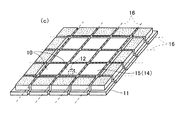
図1B(c)は、基板11および樹脂層15を切断する様子を示す図である。封止樹脂14が硬化して形成された樹脂層15および基板11をダイシングマシンなどによって予め定める切断線16に沿って切断する。本実施の形態では、基板11表面に設けられる複数のチップ12が1個ずつ含まれるように、基板11および樹脂層15を切断し、個々の電子部品10に分割する。このとき、枠部材1も各電子部品10から切り離される。以上のようにして、回路素子を含むチップ12を樹脂層15で被覆してなる電子部品10が得られる。
FIG. 1B (c) is a diagram illustrating a state in which the
以上のように、本実施の形態の電子部品の製造方法では、図1A(b)に示す工程において凹所13に供給されるべき封止樹脂14が枠部材1の外側に溢流することを防止し、封止樹脂14による基板11の裏面に設けられる端子電極などの汚染および樹脂供給装置などの生産能力の低下を防ぐことができる。したがって、端子電極などの機能不良がなく、安定して動作する電子部品10を歩留良く製造することができる。このように動作安定性に優れる電子部品10を含む電子回路を搭載することによって、安定して動作可能な信頼性に優れる電子機器を実現することができる。
As described above, in the electronic component manufacturing method of the present embodiment, the sealing
また本実施の形態では、枠部材1は、図1A(a)に示す工程において予め定められる形状の金型に液状樹脂を充填して成形することによって、基板11のチップ12が実装される表面に直接形成される。このようにして枠部材を形成することによって、本実施の形態で用いられる枠部材1のように、凹所13に供給されるべき封止樹脂14の溢流防止に好適な、複雑な形状を有する枠部材を容易に形成することができる。また基板11のチップ12が実装される表面と枠部材1との間に隙間が生じることを防ぎ、前記隙間からの封止樹脂14の漏出を防止することができる。また高さの均一な枠部材1を形成し、封止樹脂14が硬化して形成される樹脂層15の表面の平坦性を向上させることができるので、電子部品10の不良の発生を抑えることができる。たとえば光ピックアップ装置に備わる電子部品のように、チップ12表面に受光素子を備え、受光素子を被覆する樹脂層15の表面が受光面となる電子部品10を製造する場合には、樹脂層15の表面が受光素子の受光面に対して傾くことを防ぎ、光学特性の不良の発生を抑えることができる。
Further, in the present embodiment, the
なお、枠部材1は、予め別工程で作製されて基板11のチップ12が実装される表面に貼り付けられてもよい。この場合には、片面に粘着性を有するシート状の枠材料を所定の形状に加工して枠部材1とし、これを基板11のチップ12が実装される表面に貼り付けることによって、基板11表面に枠部材1を配設することができる。このような片面に粘着性を有する枠材料としては、たとえばシリコーンゴムなどの、樹脂に対して離型性を有する材料をシート状に加工したものに、樹脂などからなるシート状の基材の両面に粘着剤層が形成されてなる両面粘着シートを貼り合わせたものなどが用いられる。
The
ただし、基板11のチップ12が実装される表面と枠部材1との密着性、枠部材1の高さの均一性などを考慮すると、本実施形態のように基板11のチップ12が実装される表面に直接枠部材1を形成する方が好ましい。
However, considering the adhesion between the surface of the
また、本実施の形態では、図1B(c)に示す工程において、基板11表面に設けられる複数のチップ12が1個ずつ含まれるように基板11および樹脂層15を切断するけれども、チップ12が2個以上ずつ含まれるように基板11および樹脂層15を切断してもよい。また本実施の形態では、複数の電子部品10を同時に作製するけれども、1個ずつ作製してもよい。
In the present embodiment, in the step shown in FIG. 1B (c), the
図2は、本発明の実施の第2形態である電子部品の製造方法に用いられる枠部材2の構造を模式的に示す斜視図である。本実施の形態の電子部品の製造方法では、前述の図1A(a)に示す工程において図2に示す枠部材2を基板11表面に設けること以外は、実施の第1形態の電子部品の製造方法と同様にして電子部品を製造する。
FIG. 2 is a perspective view schematically showing the structure of the
本実施の形態による枠部材2において注目すべきは、枠部材2の凹所13に臨む壁部2bが、基板11のチップ12が実装される表面から遠ざかるにつれて凹所13の外方に向かって傾斜していることである。
It should be noted in the
本実施の形態では、枠部材2の凹所13に臨む壁部2bは、基板11に接しない面2aに交わり、かつ凹所13の外方に向かって傾斜する傾斜部20と、基板11のチップ12が実装される表面に略垂直に交わる垂直壁部21とを含んで構成される。ここで、「略垂直」とは、垂直を含む。
In the present embodiment, the
また、枠部材2の凹所13に臨む壁部2bに交わりかつ基板11に接しない面2aは、実施の第1形態による枠部材1と同様に、基板11のチップ12が実装される表面よりも摩擦抵抗が大きくなるように形成される。
Further, the
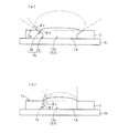
図3は、凹所13に封止樹脂14を供給する際の状態について、枠部材の凹所13に臨む壁部が凹所の外方に向かって傾斜している場合と傾斜していない場合とを対比して説明する図である。図3(a)には、枠部材の凹所13に臨む壁部が傾斜している場合として本実施の形態による枠部材2を用いた場合を示し、図3(b)には、枠部材の凹所13に臨む壁部が傾斜していない場合として実施の第1形態による枠部材1を用いた場合を示す。なお、図3(a)は、図2に示す枠部材2を切断面線II−IIから見て示す断面図であり、図3(b)は、図1A(a)に示す枠部材1を切断面線I−Iから見て示す断面図である。また図3では、説明の便宜上、凹所13の一部を除いた形で示す。
FIG. 3 shows the state when the sealing
枠部材2と基板11のチップ12が実装される表面とによって形成される凹所13a、および枠部材1と基板11の前記表面とによって形成される凹所13bに、同量の封止樹脂14を供給すると、凹所13a,13b(以下、特に区別する必要がある場合を除いて凹所13と総称する)に供給された封止樹脂14の表面は、図3の実線で示される円弧状になる。このときの凹所13に供給された封止樹脂14と枠部材の凹所13に臨む壁部との接触角θを比較すると、図3(a)に示す枠部材2の凹所13aに臨む壁部2bが凹所13aの外方に向かって傾斜している場合の接触角θ2の方が、図3(b)に示す枠部材1の凹所13に臨む壁部1bが傾斜していない場合の接触角θ1よりも小さくなる。
The same amount of sealing
このため、凹所13aおよび13bに、凹所13に供給された封止樹脂14と凹所13に臨む壁部との接触角θが、凹所13から封止樹脂14が溢流し始めるときの前記接触角(オーバーフロー臨界角θc)に達する直前まで封止樹脂14を供給すると、凹所13に供給された封止樹脂14の表面は、図3の点線で示される円弧状になる。
For this reason, the contact angle θ between the sealing
図3(a)と図3(b)との比較から明らかなように、図3(a)に示す本実施の形態では、凹所13aに供給された封止樹脂14と凹所13aに臨む壁部2bとの接触角θがオーバーフロー臨界角θcに達するまでに凹所13aに供給することのできる封止樹脂14の量を、図3(b)に示す枠部材1の凹所13bに臨む壁部1bが凹所13bの外方に向かって傾斜していない場合よりも増加させることができる。
As is clear from a comparison between FIG. 3A and FIG. 3B, the present embodiment shown in FIG. 3A faces the sealing
ただし、凹所13に供給された封止樹脂14の表面が図3の実線で示される円弧状になるように、枠部材1,2の高さを超える位置まで封止樹脂14を供給すると、基板11の傾きおよび揺れなどによって封止樹脂14の溢流が生じやすくなる。しかしながら、本実施の形態では、基板11に傾きおよび揺れが生じても、封止樹脂14と枠部材2の凹所13aを臨む壁部2bとの接触角θはオーバーフロー臨界角θcに達しにくいので、封止樹脂14の溢流を防止することができる。すなわち、本実施の形態では、図3(b)に示す枠部材1の凹所13bに臨む壁部1bが傾斜していない場合に比べ、基板11の傾きおよび揺れなどによる封止樹脂14の溢流をより確実に防ぐことができる。
However, when the sealing
したがって、本実施の形態では、封止樹脂14の枠部材2の外側への溢流を生じさせることなく、凹所13に供給する封止樹脂14の量を増加させることが可能であり、封止樹脂14の蒸発による樹脂層15の厚みの設計値からのずれを抑えることができる。
Therefore, in this embodiment, it is possible to increase the amount of the sealing
なお、本実施の形態では、枠部材2は、凹所13に臨む壁部2bが傾斜部20と垂直壁部21とを含み、基板11に接しない面2a近傍の壁部2bのみが傾斜している形状であるけれども、これに限定されることなく、少なくとも基板11に接しない面2a近傍の壁部2bが、基板11のチップ12が実装される表面から遠ざかるにつれて凹所13の外方に向かって傾斜している形状であればどのような形状であってもよい。たとえば、枠部材2の凹所13に臨む壁部2b全体が、基板11のチップ12が実装される表面から遠ざかるにつれて凹所13の外方に向かって傾斜している形状であってもよい。
In the present embodiment, the
図4は、本発明の実施の第3形態である電子部品の製造方法に用いられる枠部材3の構成を模式的に示す斜視図である。本実施の形態の電子部品の製造方法では、前述の図1A(a)に示す工程において図4に示す枠部材3を基板11表面に設けること以外は、実施の第1形態の電子部品の製造方法と同様にして電子部品を製造する。
FIG. 4 is a perspective view schematically showing a configuration of the frame member 3 used in the electronic component manufacturing method according to the third embodiment of the present invention. In the electronic component manufacturing method of the present embodiment, the electronic component manufacturing of the first embodiment is performed except that the frame member 3 shown in FIG. 4 is provided on the surface of the
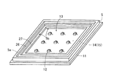
本実施の形態による枠部材3において注目すべきは、凹所13に臨む壁部3bに交わり、かつ基板11に接しない面3aに、凹所13に供給されるべき封止樹脂14を溜め得る樹脂溜り部22を有することである。
What should be noted in the frame member 3 according to the present embodiment is that the sealing
樹脂溜り部22を設けることによって、前述の図1A(b)に示す工程と同様にして凹所13に封止樹脂14を供給する際に、凹所13から枠部材3を超えて枠部材3の外側に溢流しようとする封止樹脂14を樹脂溜り部22に貯留し、凹所13に供給されるべき封止樹脂14が枠部材3の外側に溢流することを防止することができる。したがって、実施の第1形態と同様に、封止樹脂14による基板11の裏面に設けられる端子電極などの汚染および樹脂供給装置などの生産能力の低下を抑えることができるので、歩留を向上させることができる。
By providing the
本実施の形態では、樹脂溜り部22として、枠部材3の凹所13に臨む壁部3bに交わり、かつ基板11に接しない面3aに開口部を有し、前記面3aから、基板11のチップ12が実装される表面に向かって延び、枠部材13の内部の予め定める部分に達する孔部が設けられる。樹脂溜り部22は、枠部材3の凹所13に臨む壁部3bに交わり、かつ基板11に接しない面3aの各所に複数個設けられる。
In the present embodiment, the
なお、樹脂溜り部22は、これに限定されるものではなく、凹所13に供給されるべき封止樹脂14を溜め得るものであれば、どのようなものであってもよい。たとえば、枠部材3の凹所13に臨む壁部3bに交わり、かつ基板11に接しない面3aに開口部を有し、前記面3aから、枠部材3を貫通して基板11のチップ12が実装される表面に達する貫通孔を樹脂溜り部22として設けてもよい。また、枠部材3に、枠部材3の凹所13に臨む壁部3bに交わり、かつ基板11に接しない面3a側が開口部となる溝部を設け、これを樹脂溜り部22として用いてもよい。
The
また、枠部材3の凹所13に臨む壁部3bは、実施の第2形態と同様に、基板11のチップ12が実装される表面から遠ざかるにつれて凹所13の外方に向かって傾斜していてもよい。
Further, the wall 3b facing the
図5は、本発明の実施の第4形態である電子部品の製造方法に用いられる枠部材4の構成を模式的に示す斜視図である。本実施の形態の電子部品の製造方法では、前述の図1A(a)に示す工程において図5に示す枠部材4を基板11表面に設け、後述する平坦部25の高さを超える位置まで封止樹脂14を供給すること以外は、実施の第1形態の電子部品の製造方法と同様にして電子部品を製造する。
FIG. 5 is a perspective view schematically showing the configuration of the
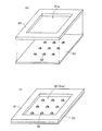
本実施の形態による枠部材4において注目すべきは、凹所13に臨む壁部4bが、基板11のチップ12が実装される表面から遠ざかるにつれて凹所13の平面積が大きくなるように、厚み方向に段差部23を有することである。
It should be noted in the
本実施の形態では、段差部23は、基板11のチップ12が実装される表面に略垂直に交わる垂直壁部24と、垂直壁部24に略垂直に交わる平坦部25とを含んで構成される。枠部材4は、平坦部25の高さ、すなわち平坦部25から基板11のチップ12が実装される表面までの距離が、樹脂層15の厚みとして所望される値に略等しくなるように形成される。
In the present embodiment, the
本実施の形態において、前述の図1A(b)に示す工程と同様にして凹所13に封止樹脂14を供給する際には、前述のように平坦部25の高さを超える位置まで封止樹脂14を供給する。このとき、平坦部25の高さを超える位置に供給された封止樹脂14は、段差部23の平坦部25の上方に貯留されるので、凹所13から枠部材4を超えて枠部材4の外側に溢流することはない。すなわち、本実施の形態では、凹所13に供給されるべき封止樹脂14が枠部材4を超えて枠部材4の外側に溢流することを防止することができる。したがって、実施の第1形態と同様に、封止樹脂14による基板11の裏面に設けられる端子電極などの汚染および樹脂供給装置などの生産能力の低下を抑えることができるので、電子部品を歩留良く製造することができる。
In the present embodiment, when the sealing
また、本実施の形態では、平坦部25を目安として封止樹脂14の供給量を調整することができる。すなわち、封止樹脂14が平坦部25の上方まで供給された時点で封止樹脂14の供給を止めることができる。したがって、均一な厚みを有する樹脂層15を形成することができる。
In the present embodiment, the supply amount of the sealing
これに対し、枠部材として、単にその高さが樹脂層15の厚みとして所望される値よりも大きくなるように形成されたものを用いる場合には、枠部材の外側への封止樹脂14の溢流を防ぐことは可能であるけれども、封止樹脂14の供給量の調整が困難になる。このため、樹脂層の厚みにばらつきが生じ、電子部品の不良が発生するおそれがある。したがって、このような観点からも、本実施の形態のように凹所13に臨む壁部4bには厚み方向に段差部23を設けることが好ましい。
On the other hand, when using a frame member formed such that its height is larger than a desired value as the thickness of the
なお、本実施の形態では、枠部材4の凹所13に臨む壁部4bの厚み方向には1個の段差部23が設けられるけれども、これに限定されることなく、複数の段差部が設けられてもよい。たとえば、図6に示す枠部材5のように、凹所13に臨む壁部5bに交わり、かつ基板11に接しない面5a側から順に、第1段差部26および第2段差部27の2個の段差部が設けられてもよい。
In the present embodiment, one
枠部材5のように、凹所13に臨む壁部5bの厚み方向に、複数の段差部を設けることによって、前述の図1A(b)に示す工程と同様にして凹所13に封止樹脂14を供給する際に、第1段差部26または第2段差部27などの各段差部を目安として、凹所13に供給する封止樹脂14の量を調整することができる。すなわち、段差部を構成する平坦部の基板11のチップ12が実装される表面からの高さ(以下、段差部の高さと称する)を、樹脂層15の厚みとして所望される値に略等しくなるように選択することによって、樹脂層15の厚みを容易に所望の値にすることができる。たとえば、図6に示す第2段差部27を目安として、封止樹脂14が第2段差部27の高さを超えるまで凹所13に封止樹脂14を供給することによって、第1段差部26の高さを超える位置まで封止樹脂14を供給する場合よりも薄い樹脂層15を形成することができる。したがって、凹所13に供給されるべき封止樹脂14が枠部材5の外側に溢流することを防ぐとともに、種々の厚みを有する樹脂層15を容易に形成することができる。
Like the
また、枠部材4,5の凹所13に臨む壁部4b,5bは、実施の第2形態と同様に、基板11のチップ12が実装される表面から遠ざかるにつれて凹所13の外方に向かって傾斜していてもよい。
Further, the
1,2,3,4,5 枠部材
10 電子部品
11 基板
12 チップ
13 凹所
14 封止樹脂
15 樹脂層
20 傾斜部
22 樹脂溜り部
23 段差部
26 第1段差部
27 第2段差部
1, 2, 3, 4, 5
Claims (8)
樹脂供給工程では、
基板の回路素子が設けられる表面に、基板の前記表面を底部として樹脂を供給すべき凹所を形成し得る枠部材であって、前記凹所に臨む壁部に交わり、かつ基板に接しない面の摩擦抵抗が、基板の回路素子が設けられる表面の摩擦抵抗よりも大きくなるように形成される枠部材を、回路素子を囲むように設け、
枠部材と基板の前記表面とによって形成される凹所に樹脂を供給することを特徴とする電子部品の製造方法。 An element disposing step of providing a circuit element on one surface of the substrate, a resin supplying step of supplying a resin so as to cover the circuit element on the surface of the substrate on which the circuit element is provided, and a resin supplied to the surface of the substrate A method of manufacturing an electronic component, including a resin curing step for curing, and manufacturing an electronic component including a circuit element coated with a resin,
In the resin supply process,
A frame member capable of forming a recess to which resin should be supplied with the surface of the substrate as a bottom portion on a surface on which a circuit element of the substrate is provided, and is a surface that intersects with a wall facing the recess and does not contact the substrate A frame member formed so that the frictional resistance of the substrate is larger than the frictional resistance of the surface on which the circuit element of the substrate is provided is provided so as to surround the circuit element,
Resin is supplied to the recess formed by a frame member and the said surface of a board | substrate, The manufacturing method of the electronic component characterized by the above-mentioned.
1μm以上、5μm以下であることを特徴とする請求項1記載の電子部品の製造方法。 The ten-point average roughness Rz of the surface that intersects the wall facing the recess of the frame member and does not contact the substrate is
The method of manufacturing an electronic component according to claim 1, wherein the method is 1 μm or more and 5 μm or less.
樹脂供給工程では、
基板の回路素子が設けられる表面に、基板の前記表面を底部として樹脂を供給すべき凹所を形成し得る枠部材であって、前記凹所に臨む壁部に交わり、かつ基板に接しない面に前記凹所に供給されるべき樹脂を溜め得る樹脂溜り部を有するように形成される枠部材を、回路素子を囲むように設け、
枠部材と基板の前記表面とによって形成される凹所に樹脂を供給することを特徴とする電子部品の製造方法。 An element disposing step of providing a circuit element on one surface of the substrate, a resin supplying step of supplying a resin so as to cover the circuit element on the surface of the substrate on which the circuit element is provided, and a resin supplied to the surface of the substrate A method of manufacturing an electronic component, including a resin curing step for curing, and manufacturing an electronic component including a circuit element coated with a resin,
In the resin supply process,
A frame member capable of forming a recess to which resin should be supplied with the surface of the substrate as a bottom portion on a surface on which a circuit element of the substrate is provided, and is a surface that intersects with a wall facing the recess and does not contact the substrate A frame member formed so as to have a resin reservoir that can store the resin to be supplied to the recess, so as to surround the circuit element;
Resin is supplied to the recess formed by a frame member and the said surface of a board | substrate, The manufacturing method of the electronic component characterized by the above-mentioned.
樹脂供給工程では、
基板の回路素子が設けられる表面に、基板の前記表面を底部として樹脂を供給すべき凹所を形成し得る枠部材であって、基板の回路素子が設けられる表面から遠ざかるにつれて前記凹所の平面積が大きくなるように、前記凹所に臨む壁部が厚み方向に段差部を有するように形成される枠部材を、回路素子を囲むように設け、
枠部材と基板の前記表面とによって形成される凹所に樹脂を供給することを特徴とする電子部品の製造方法。 An element disposing step of providing a circuit element on one surface of the substrate, a resin supplying step of supplying a resin so as to cover the circuit element on the surface of the substrate on which the circuit element is provided, and a resin supplied to the surface of the substrate A method of manufacturing an electronic component, including a resin curing step of curing, and manufacturing an electronic component including a circuit element coated with a resin,
In the resin supply process,
A frame member capable of forming a recess to be supplied with resin with the surface of the substrate as a bottom portion on a surface of the substrate on which the circuit element is provided, and as the distance from the surface on which the circuit element of the substrate is provided becomes flat. A frame member formed so that the wall portion facing the recess has a step portion in the thickness direction so as to increase the area is provided so as to surround the circuit element,
Resin is supplied to the recess formed by a frame member and the said surface of a board | substrate, The manufacturing method of the electronic component characterized by the above-mentioned.
Priority Applications (1)
| Application Number | Priority Date | Filing Date | Title |
|---|---|---|---|
| JP2004107505A JP2005294529A (en) | 2004-03-31 | 2004-03-31 | Electronic component manufacturing method and electronic device |
Applications Claiming Priority (1)
| Application Number | Priority Date | Filing Date | Title |
|---|---|---|---|
| JP2004107505A JP2005294529A (en) | 2004-03-31 | 2004-03-31 | Electronic component manufacturing method and electronic device |
Publications (1)
| Publication Number | Publication Date |
|---|---|
| JP2005294529A true JP2005294529A (en) | 2005-10-20 |
Family
ID=35327122
Family Applications (1)
| Application Number | Title | Priority Date | Filing Date |
|---|---|---|---|
| JP2004107505A Pending JP2005294529A (en) | 2004-03-31 | 2004-03-31 | Electronic component manufacturing method and electronic device |
Country Status (1)
| Country | Link |
|---|---|
| JP (1) | JP2005294529A (en) |
Cited By (1)
| Publication number | Priority date | Publication date | Assignee | Title |
|---|---|---|---|---|
| US11757062B2 (en) | 2019-09-10 | 2023-09-12 | Nichia Corporation | Method for manufacturing light emitting device using reinforcement member |
-
2004
- 2004-03-31 JP JP2004107505A patent/JP2005294529A/en active Pending
Cited By (1)
| Publication number | Priority date | Publication date | Assignee | Title |
|---|---|---|---|---|
| US11757062B2 (en) | 2019-09-10 | 2023-09-12 | Nichia Corporation | Method for manufacturing light emitting device using reinforcement member |
Similar Documents
| Publication | Publication Date | Title |
|---|---|---|
| JP6671441B2 (en) | Electronic component storage package, multi-cavity wiring board, electronic device and electronic module | |
| TWI611524B (en) | Stacked package electronic component including sealing layer and related manufacturing method | |
| TWI500181B (en) | Base of optoelectronic device | |
| US11837557B2 (en) | Semiconductor device package and a method of manufacturing the same | |
| TWI726230B (en) | Holding member, method of manufacturing holding member, holding mechanism, and product manufacturing device | |
| CN101060091A (en) | Method and system for providing conductive bonding material | |
| TWI818655B (en) | Semiconductor device and method of manufacturing semiconductor device | |
| KR20130087249A (en) | Semiconductor apparatus and image sensor package using the same | |
| US11101189B2 (en) | Semiconductor device package and method of manufacturing the same | |
| US10062815B1 (en) | Light emitting device and method of manufacturing the same | |
| US20090267214A1 (en) | Electronic circuit device and method for manufacturing same | |
| CN100508201C (en) | Package for solid image pickup element and solid image pickup device | |
| US12249546B2 (en) | Electronic element mounting substrate and electronic device | |
| JP2005294529A (en) | Electronic component manufacturing method and electronic device | |
| CN108281566B (en) | OLED panel and manufacturing method thereof | |
| JP2020174148A (en) | Manufacturing method of component-embedded board and component-embedded board | |
| CN106505043A (en) | The manufacture method and manufacture device of semiconductor device | |
| US20210351151A1 (en) | Circuit Carrier Having an Installation Place for Electronic Components, Electronic Circuit and Production Method | |
| JP7101309B2 (en) | Package for storing electronic components | |
| US20070200214A1 (en) | Board strip and method of manufacturing semiconductor package using the same | |
| CN102549741A (en) | Semiconductor device and method for manufacturing same | |
| JP2007173561A (en) | Method for manufacturing light emitting device | |
| US12494419B2 (en) | Integrated circuit package with warpage control using cavity formed in laminated substrate below the integrated circuit die | |
| US11984385B2 (en) | Lead frame structure and manufacturing method thereof | |
| JP2001291729A (en) | Method for sealing semiconductor element with resin by stencil printing, and stencil printing plate and squeegee used therefor |
Legal Events
| Date | Code | Title | Description |
|---|---|---|---|
| A621 | Written request for application examination |
Free format text: JAPANESE INTERMEDIATE CODE: A621 Effective date: 20060125 |
|
| A977 | Report on retrieval |
Free format text: JAPANESE INTERMEDIATE CODE: A971007 Effective date: 20061226 |
|
| A131 | Notification of reasons for refusal |
Free format text: JAPANESE INTERMEDIATE CODE: A131 Effective date: 20071120 |
|
| A521 | Request for written amendment filed |
Free format text: JAPANESE INTERMEDIATE CODE: A523 Effective date: 20080121 |
|
| A02 | Decision of refusal |
Free format text: JAPANESE INTERMEDIATE CODE: A02 Effective date: 20080219 |