JP2005294493A - Laser process and laser annealing equipment - Google Patents
Laser process and laser annealing equipment Download PDFInfo
- Publication number
- JP2005294493A JP2005294493A JP2004106770A JP2004106770A JP2005294493A JP 2005294493 A JP2005294493 A JP 2005294493A JP 2004106770 A JP2004106770 A JP 2004106770A JP 2004106770 A JP2004106770 A JP 2004106770A JP 2005294493 A JP2005294493 A JP 2005294493A
- Authority
- JP
- Japan
- Prior art keywords
- laser
- output
- oscillator
- optical system
- excitation
- Prior art date
- Legal status (The legal status is an assumption and is not a legal conclusion. Google has not performed a legal analysis and makes no representation as to the accuracy of the status listed.)
- Withdrawn
Links
Images
Landscapes
- Recrystallisation Techniques (AREA)
- Thin Film Transistor (AREA)
Abstract
【課題】 高品質の薄膜トランジスタの活性層の形成するためのレーザプロセスとそれを用いたレーザアニール装置を提供すること。
【解決手段】 レーザ発振器1a〜1eを制御する出力制御部は、各レーザ発振器1a〜1eの出力が一定になるよう、かつ、加工点のパワーが予め定められている所定のパワーになるように制御し、また、励起用のLDの寿命予測をおこなう。
【選択図】 図1PROBLEM TO BE SOLVED: To provide a laser process for forming an active layer of a high quality thin film transistor and a laser annealing apparatus using the same.
An output control unit that controls laser oscillators 1a to 1e is configured so that the outputs of the laser oscillators 1a to 1e are constant and the power of a processing point is a predetermined power. Control the lifetime of the LD for excitation.
[Selection] Figure 1
Description
本発明は、高品質の薄膜トランジスタの活性層の形成に関し、特に、p−Si(ポリ−シリコン)のTFT(Thin Film Transistor)の製造で、レーザ光を用いてガラス基板上のa−Si(アモルファス−シリコン)薄膜をポリ化して高品質のp−Si薄膜を形成する技術に関する。 The present invention relates to the formation of an active layer of a high-quality thin film transistor, and in particular, in the manufacture of TFT (Thin Film Transistor) of p-Si (poly-silicon), a-Si (amorphous) on a glass substrate using laser light. (Silicon) The present invention relates to a technology for forming a high-quality p-Si thin film by polymorphizing the thin film.
通常、液晶ディスプレイや有機ELディスプレイにおいては、薄膜トランジスタをポリシリコンによって形成することにより、スイッチング素子や駆動用周辺回路をガラス基板上に形成している。液晶ディスプレイではより高精細化や高速応答性や低消費電力化した次世代の高機能液晶ディスプレイが求められている。 Usually, in a liquid crystal display or an organic EL display, a switching element and a driving peripheral circuit are formed on a glass substrate by forming a thin film transistor from polysilicon. There is a need for next-generation high-performance liquid crystal displays with higher definition, higher speed response, and lower power consumption.
これら技術の実現のためには、電界移動度(μFE)が1cm2/Vs以下と低いアモルファスシリコンの薄膜トランジスタでは能力が十分ではない。薄膜トランジスタの活性層の形成方法として、絶縁表面を有する基板上に非晶質半導体膜を形成し、レーザアニール法や熱アニール法などで結晶化させる技術が開発されている。 In order to realize these technologies, the amorphous silicon thin film transistor whose electric field mobility (μFE) is as low as 1 cm 2 / Vs or less is not sufficient. As a method for forming an active layer of a thin film transistor, a technique has been developed in which an amorphous semiconductor film is formed on a substrate having an insulating surface and crystallized by a laser annealing method, a thermal annealing method, or the like.
レーザアニール法はガラス基板の温度をあまり上昇させず、非晶質半導体膜にのみ高いエネルギーを与えて結晶化させることができる結晶化技術として知られている。特に、波長400nm以下の短波長光を発振するエキシマレーザは、このレーザアニール法の開発当初から用いられてきた代表的なレーザである。レーザアニール法は、レーザビームを被照射面においてスポット状や線状となるように光学系で加工し、その加工されたレーザ光で基板上の被照射面を走査すること(レーザ光の照射位置を被照射面に対して相対的に移動させる)により行う。 The laser annealing method is known as a crystallization technique that does not raise the temperature of a glass substrate so much and can crystallize only an amorphous semiconductor film by applying high energy. In particular, an excimer laser that oscillates short-wavelength light having a wavelength of 400 nm or less is a typical laser that has been used from the beginning of the development of this laser annealing method. In the laser annealing method, a laser beam is processed by an optical system so as to be spot-like or linear on the irradiated surface, and the irradiated surface on the substrate is scanned with the processed laser beam (the position of the irradiated laser beam). Is moved relative to the irradiated surface).
レーザアニール法で、例えば、アモルファスシリコンにエキシマレーザを照射してラテラル成長させる製造した多結晶シリコン半導体であるポリシリコンの薄膜トランジスタであれば、電界移動度が100cm2/Vs〜200cm2/Vs程度のものが得られる。それによれば、液晶ディスプレイの高精彩化、高速化および駆動回路の一体形成などの高機能化が期待できる。 In laser annealing, for example, if the polysilicon thin film transistor is a polycrystalline silicon semiconductor fabricated in amorphous silicon is irradiated with an excimer laser to lateral growth, the electric field mobility is 100cm 2 / Vs~200cm of about 2 / Vs Things are obtained. According to this, it is expected that the liquid crystal display has higher functions such as higher definition, higher speed, and integral formation of drive circuits.
このエキシマレーザ法は、透光性基板であるガラス基板上のアモルファスシリコンにエキシマレーザを照射してポリシリコンとする方法である。具体的には、アモルファスシリコンの表面でのビームサイズを、例えば長さ250mm、幅0.4mmにし、このパルスビームを300Hzで発振させて、各パルスの照射される領域を徐々に移動させることにより、ガラス基板上のアモルファスシリコンをポリシリコンにする(例えば、特許文献1を参照)。 This excimer laser method is a method in which amorphous silicon on a glass substrate which is a light-transmitting substrate is irradiated with an excimer laser to form polysilicon. Specifically, the beam size on the surface of amorphous silicon is set to, for example, a length of 250 mm and a width of 0.4 mm, and this pulse beam is oscillated at 300 Hz to gradually move the region irradiated with each pulse. Then, amorphous silicon on the glass substrate is changed to polysilicon (for example, see Patent Document 1).
また、エキシマレーザの替わりに、レーザ媒質として固体レーザであるYAGレーザを用いてレーザアニールをおこなっている技術も開示されている(例えば、特許文献2を参照)。 Further, a technique is disclosed in which laser annealing is performed using a YAG laser that is a solid-state laser as a laser medium instead of an excimer laser (see, for example, Patent Document 2).
また、最近、CW−SHGレーザ(波長532nm)を用いたラテラル成長法が提案され、移動度の高いp−SiのTFTが得られるとの報告もある。
上述のように、薄膜トランジスタの活性層の形成方法として、絶縁表面を有する基板上に非晶質半導体膜を形成し、レーザアニール法で結晶化させる場合、エキシマレーザによるラテラル成長は、量産ラインでの実績がある従来プロセスと加工光源が同じであるため量産ラインに適用しやすいというメリットがあるが、メンテナンスコストが高いという問題が課題として残っている。 As described above, as a method for forming an active layer of a thin film transistor, when an amorphous semiconductor film is formed on a substrate having an insulating surface and crystallized by a laser annealing method, lateral growth by an excimer laser is performed on a mass production line. There is a merit that it is easy to apply to a mass production line because the processing light source is the same as the conventional process that has a proven record, but the problem of high maintenance cost remains as a problem.
一方、固体レーザによるラテラル成長は、高い膜質(高移動度)が得られ、設備コストやランニングコストが低く抑えられるために、もし、量産ラインへ適用した場合のメリットは大きいと考えられるが、これまでに量産ラインでは、殆ど実績がないために克服すべき技術課題が多く、現時点では量産ラインへの適用が困難、あるいは、長い開発期間が必要であるという問題が存在する。 On the other hand, lateral growth using a solid-state laser can provide high film quality (high mobility), and the equipment and running costs can be kept low. In the mass production line, there are many technical problems to be overcome because there are almost no achievements, and there is a problem that it is difficult to apply to the mass production line or a long development period is required at present.
また、CW−SHG(第二高調波)レーザ(波長532nm)を用いたラテラル成長法では、移動度の高いp−SiのTFTが得られると報告されているが、CW−SHGレーザ1台から出力されるパワーは現在、実用レベルで10Wしかなく、量産に必要な数百ワットレベルを達成することは1台では困難である。したがって、複数台のレーザ装置を必要とすることは避けられない。その場合、複数台のレーザ光源のメンテナンスおよびビーム合成時の干渉縞発生、およびビーム走査時のビームエッジ部での微小結晶発生およびビームの高速スイッチングに大きな課題が残っている。 Further, it has been reported that a lateral growth method using a CW-SHG (second harmonic) laser (wavelength 532 nm) can obtain a p-Si TFT with high mobility, but from one CW-SHG laser. Currently, the output power is only 10 W at a practical level, and it is difficult to achieve the several hundred watt level necessary for mass production. Therefore, it is inevitable that a plurality of laser devices are required. In that case, there are still significant problems in maintenance of a plurality of laser light sources and generation of interference fringes during beam synthesis, generation of microcrystals at the beam edge portion during beam scanning, and high-speed beam switching.
すなわち、現在の商用エキシマレーザの出力は約300Wに達しており、この300Wを達成するためには、10WのSHGレーザを用いると30台が必要となる。SHGレーザは通常LD(レーザダイオード)励起のYAGレーザが用いられている。LDは交換部品であり、通常、LDの交換は10000Hごとの実施が必要であり、約1年ごとの交換となる。もしこのLDの交換が、30台のレーザ装置でランダムに発生すると、場合によっては12日ごとのメンテナンスダウンタイムが発生してしまう。これではLD励起方式レーザの特徴であるメンテナンスフリーがアニールシステムの特徴として生かすことができない。 That is, the output of the current commercial excimer laser has reached about 300 W, and in order to achieve this 300 W, 30 units are required if a 10 W SHG laser is used. As an SHG laser, an LD (laser diode) pumped YAG laser is usually used. The LD is a replacement part. Normally, the LD needs to be replaced every 10000H, and is replaced every year. If this LD replacement occurs randomly in 30 laser devices, a maintenance downtime every 12 days may occur in some cases. In this case, the maintenance-free characteristic of the LD excitation laser cannot be utilized as a characteristic of the annealing system.
一方、複数台のレーザから出力されるビームを重ね合わせる場合、SHGレーザの可干渉性の高さから干渉縞発生は避けられず、通常エキシマレーザで使用されているアレイレンズ式のホモジナイザを用いた場合、加工点で重ね合わせ方向にNA(開口角)に応じた間隔で強度の変調が生じてしまう。これは結晶化のむらにつながり、TFT特性のばらつきを増長させる要因になる。 On the other hand, when superimposing beams output from a plurality of lasers, interference fringes are unavoidable due to the high coherence of the SHG laser, and an array lens type homogenizer usually used in excimer lasers was used. In this case, intensity modulation occurs at intervals corresponding to NA (opening angle) in the overlapping direction at the processing point. This leads to uneven crystallization and increases the variation in TFT characteristics.
同様に結晶化のむらに関しては、ラインビーム長手方向の特にビームエッジ部分でのスティープネス不足により、ラインビーム中央付近はラテラル成長が進むものの、ビームエッジ部では微結晶が発生することもTFT特性はばらつきの要因となる。さらに結晶化を基板の局所領域に施す場合、CWレーザの加工点でのON/OFFのレスポンス時間が長いと走査の開始、終了時点で微結晶が生じることになる。CWラテラル方式の走査速度は1000mm/sにも達するため、1msecでスイッチングできても、1mmの長さの微結晶領域が発生する。 Similarly, with regard to uneven crystallization, although the lateral growth proceeds near the center of the line beam due to insufficient steepness in the longitudinal direction of the line beam, particularly in the beam edge portion, micro-crystals are also generated at the beam edge portion. It becomes a factor of. Further, when crystallization is performed on a local region of the substrate, if the ON / OFF response time at the processing point of the CW laser is long, microcrystals are generated at the start and end of scanning. Since the scanning speed of the CW lateral method reaches 1000 mm / s, a microcrystalline region with a length of 1 mm is generated even if switching can be performed at 1 msec.
本発明はこれらの事情にもとづいてなされたもので、高品質の薄膜トランジスタの活性層の形成するためのレーザプロセスとそれを用いたレーザアニール装置を提供することを目的としている。 The present invention has been made based on these circumstances, and an object thereof is to provide a laser process for forming an active layer of a high-quality thin film transistor and a laser annealing apparatus using the laser process.
本発明によれば、LDの励起によるレーザ発振器を並列に複数配置して、前記各レーザ発振器の出射光軸上の前方に、前記各レーザ発振器から発振されたレーザビームを合成して加工点へ導く光学系と、前記レーザビームを監視するモニタが配置され、前記モニタおよび前記LDの電流を監視する電流モニタからの出力にもとづいて出力制御部により前記各レーザ発振器から発振したレーザビームが制御されているレーザプロセスであって、
前記出力制御部は、前記各レーザ発振器の出力が一定になるよう、かつ、前記加工点のパワーが予め定められている所定のパワーになるように制御し、また、励起用のLDの寿命予測をおこなっていることを特徴とするレーザプロセスである。
According to the present invention, a plurality of laser oscillators by LD excitation are arranged in parallel, and the laser beams oscillated from the laser oscillators are synthesized in front of the output optical axis of the laser oscillators to the processing point. A guiding optical system and a monitor for monitoring the laser beam are arranged, and the laser beam oscillated from each laser oscillator is controlled by an output control unit based on outputs from the monitor and a current monitor for monitoring the current of the LD. A laser process,
The output control unit controls the output of each laser oscillator to be constant and the power of the processing point to a predetermined power, and predicts the life of the excitation LD. It is a laser process characterized by performing.
また本発明によれば、前記出力制御部による、前記加工点のパワーが予め定められている所定のパワーになるような制御は、加工点パワーモニタからデータを受け、予め定められている所定のパワーになるように、個々のレーザ発振器に対応したバリアブルアッテネータを同じ割合で調整することによりおこなっていることを特徴とするレーザプロセスである。 Further, according to the present invention, the control by the output control unit so that the power of the machining point becomes a predetermined power is determined by receiving data from the machining point power monitor and performing a predetermined predetermined power. The laser process is characterized by adjusting the variable attenuators corresponding to the individual laser oscillators at the same ratio so as to achieve power.
また本発明によれば、並列に配置されLDの励起による複数のレーザ発振器と、この各レーザ発振器の出射光軸上の前方に順次配置された、複数の前記レーザ発振器の個々のレーザ出力を可変することのできる出力減衰器と、この出力減衰器から出力されたレーザビームを合成するビーム合成光学系と、このビーム合成光学系の光軸上の前方に配置され、ラインビームを形成する際に発生する干渉縞を低減化する音響光学変調器と、前記ビーム合成光学系からの出力されたレーザビームを均一分布のラインビームを形成するためにアレイレンズ群および集光レンズからなるビームホモジナイザと、このホモジナイザで形成されたレーザビームを再整形するビーム整形アパチャと、このビーム整形アパチャにより再整形された像を結像する結像光学系と、前記個々のレーザ発振器の出力および励起用のLDの電流を検出するモニタリング機構と、前記個々のレーザ発振器の出力をモニタする出力モニタと、前記結像光学系のレーザビームをモニタする加工点出力モニタと、出力制御部とを有し、
前記出力制御部は、前記モニタリング機構および前記出力モニタによりモニタした出力および励起用LD電流のデータから前記個々のレーザ発振器のメンテナンス時期を推定し、必要によってはメンテナンスが必要な前記レーザ発振器の稼動を停止させ、その分低下した必要パワーを他の前記レーザ発振器の出力を上昇させることで補完し、前記稼動を停止したレーザ発振器のメンテナンス時も装置全体の稼動が継続できる制御アルゴリズムを有していることを特徴とするレーザアニール装置である。
Further, according to the present invention, a plurality of laser oscillators arranged in parallel and excited by LDs, and individual laser outputs of the plurality of laser oscillators arranged sequentially forward on the output optical axis of each laser oscillator can be varied. Output attenuator, a beam synthesis optical system for synthesizing the laser beam output from the output attenuator, and disposed in front of the optical axis of the beam synthesis optical system to form a line beam. An acousto-optic modulator for reducing generated interference fringes, a beam homogenizer comprising an array lens group and a condenser lens to form a uniformly distributed line beam from the laser beam output from the beam synthesis optical system; A beam shaping aperture that reshapes the laser beam formed by this homogenizer, and an image that forms an image reshaped by this beam shaping aperture A system, a monitoring mechanism for detecting the output of the individual laser oscillator and the current of the LD for excitation, an output monitor for monitoring the output of the individual laser oscillator, and a laser beam of the imaging optical system A machining point output monitor and an output control unit;
The output control unit estimates the maintenance time of each laser oscillator from the data monitored by the monitoring mechanism and the output monitor and the LD current for excitation, and if necessary, operates the laser oscillator that requires maintenance. It has a control algorithm that can be stopped and supplemented by increasing the output of the other laser oscillator by reducing the required power, and that the operation of the entire apparatus can be continued even during maintenance of the laser oscillator that has been stopped. This is a laser annealing apparatus.
また本発明によれば、前記各レーザ発振器から出力されるレーザビームは、可視光領域にあるとともに連続出力であることを特徴とするレーザアニール装置である。 Further, according to the present invention, the laser annealing apparatus is characterized in that the laser beam output from each of the laser oscillators is in a visible light region and has a continuous output.
また本発明によれば、前記各レーザ発振器は、LD励起方式のNd:YVO4レーザのSHG出力であるとともに、励起用LDが発振器側ではなく電源側に設置され、かつ、励起エネルギはファイバを通じてレーザ発振器に伝送されていることを特徴とするレーザアニール装置である。 Further, according to the present invention, each laser oscillator is an SHG output of an LD-pumped Nd: YVO 4 laser, the pumping LD is installed on the power supply side instead of the oscillator side, and the pumping energy is transmitted through the fiber. The laser annealing apparatus is transmitted to a laser oscillator.
また本発明によれば、前記各レーザ発振器から出力されたレーザビームの加工点のラインビーム長さ方向のスティープネスが5μm以内であり、かつ、ラインビームを長さ方向にオーバラップさせながら被加工物である基板全面および一部分を結晶化していくことを特徴とするレーザアニール装置である。 According to the present invention, the steepness in the length direction of the line beam at the processing point of the laser beam output from each laser oscillator is within 5 μm, and the workpiece is processed while overlapping the line beam in the length direction. A laser annealing apparatus characterized by crystallizing the entire surface and a part of a substrate, which is an object.
また本発明によれば、前記結像光学系は、結像位置を2次元的に走査するための偏向器がミラーとガルバノメータスキャナまたはポリゴンミラーと回転駆動用モータで構成されていることを特徴とするレーザアニール装置である。 According to the invention, the imaging optical system is characterized in that the deflector for two-dimensionally scanning the imaging position is composed of a mirror, a galvanometer scanner or a polygon mirror, and a rotation drive motor. This is a laser annealing apparatus.
また本発明によれば、前記ホモジナイザに設けられている音響光学変調器は、レーザビームのスイッチング作用を該レーザビームの光路途中で行うと共に、干渉縞の低減化のためにビームの方向を微小角で高速偏向させることを特徴とするレーザアニール装置である。 According to the invention, the acousto-optic modulator provided in the homogenizer performs the switching action of the laser beam in the middle of the optical path of the laser beam, and changes the direction of the beam to a small angle in order to reduce interference fringes. The laser annealing apparatus is characterized in that it is deflected at a high speed.
本発明によれば、高精度のレーザアニール処理を施すことができ、それにより、液晶基板等に用いるための高品質の薄膜トランジスタの活性層を形成することができる。 According to the present invention, a high-precision laser annealing treatment can be performed, whereby a high-quality thin film transistor active layer for use in a liquid crystal substrate or the like can be formed.
以下、本発明を実施するための最良の形態について、図面を参照して順次説明する。 Hereinafter, the best mode for carrying out the present invention will be sequentially described with reference to the drawings.
高品質のレーザアニールにより高品質の薄膜トランジスタの活性層の形成に際して、CW−SHGレーザ(波長532nm)を用いたラテラル成長法では、移動度の高いp−SiのTFTが得られると考えられているが、上述の「発明が解決しようとする課題」の項で述べたように、大別すると、(イ)メンテナンスおよびビーム合成に関しての対策、(ロ)干渉縞対策、および(ハ)結晶化むら対策、の3点についての課題を解決する必要がある。本発明では、解決策の基本的な考え方として、それぞれの対策を以下のように講じることにより課題を解消した。 When forming an active layer of a high-quality thin film transistor by high-quality laser annealing, it is considered that a lateral growth method using a CW-SHG laser (wavelength of 532 nm) can obtain a p-Si TFT with high mobility. However, as described in the above-mentioned section “Problems to be Solved by the Invention”, broadly speaking, (b) measures for maintenance and beam synthesis, (b) measures against interference fringes, and (c) uneven crystallization. It is necessary to solve the problems regarding the three points of countermeasures. In the present invention, as a basic idea of the solution, the problem is solved by taking each measure as follows.
(イ)メンテナンスおよびビーム合成に関しての対策
複数台のレーザ装置を用いる上で、各レーザのLD電流と出力をモニタしながらLD寿命を予測判定するとともに、寿命が近づいたらそのレーザ発振を停止し、それ以外の複数台のレーザ発振出力を増大させることで加工点パワーを補うようなインテリジェントシステムを採用した。
(B) Measures for maintenance and beam synthesis When using multiple laser devices, the LD life is predicted while monitoring the LD current and output of each laser, and when the life approaches, the laser oscillation is stopped. An intelligent system that supplements the machining point power by increasing the laser output of multiple other units was adopted.
すなわち、発振を停止したレーザはオフラインにてLD交換を行い、交換後復帰させることで、レーザメンテナンスでダウンする時間を極小化する。また、一部のレーザの停止で、加工点のラインビームの分布や位置が変化しないようなロバスト性を有する合成光学系を設けた。 In other words, the laser whose oscillation has been stopped is exchanged offline, and is restored after the exchange, thereby minimizing the time required for laser maintenance. Further, a synthesizing optical system having robustness is provided so that the distribution and position of the line beam at the processing point does not change when a part of the lasers are stopped.
(ロ)干渉縞対策
干渉縞対策として、レーザ発振器出口の光路途中に音響光学素子を個々に設置し、ビームを微小角でMHz以上の周波数で高速偏向させる。この高速偏向により加工点の干渉縞の位置が移動する。CWラテラルでは1000mm/s程度で走査するので、一箇所あたりのプロセス時間(溶融時間)は10μs程度である。音響光学素子のスイッチングのレスポンスは数十nsオーダなので、プロセス時間内で数百回以上の干渉縞の移動が生じるので、強度変調が存在しても温度分布は均一化される。
(B) Interference fringe countermeasures As an interference fringe countermeasure, an acoustooptic element is individually installed in the middle of the optical path at the exit of the laser oscillator, and the beam is deflected at a high speed with a minute angle at a frequency of MHz or higher. This high-speed deflection moves the position of the interference fringe at the machining point. Since scanning is performed at about 1000 mm / s in the CW lateral, the process time (melting time) per place is about 10 μs. Since the switching response of the acousto-optic element is on the order of several tens of ns, the interference fringes move several hundred times or more within the process time, so that the temperature distribution is made uniform even in the presence of intensity modulation.
(ハ)結晶化むら対策
結晶化むら対策は、一部が干渉縞対策とオーバラップする。干渉縞対策で使用する音響光学素子により、ラインビームの長軸方向の温度分布は均一化される。ビームエッジ部のスティープネスは結像光学系を用いることで確保する。ビームのスイッチングは音響光学素子でビーム方向を大きく偏向すること、光路途中のスリットによる大偏向ビームの遮光で実現する。スイッチングのレスポンスは前述した数十nsなので、加工点ではサブミクロンオーダとすることができる。
(C) Non-uniform crystallization countermeasures Some non-uniform crystallization countermeasures overlap with anti-interference fringe countermeasures. The acoustooptic device used for interference fringe countermeasures equalizes the temperature distribution in the long axis direction of the line beam. The steepness of the beam edge portion is ensured by using an imaging optical system. The switching of the beam is realized by largely deflecting the beam direction with an acousto-optic element and shielding the large deflection beam by a slit in the optical path. Since the switching response is several tens of ns as described above, the processing point can be on the order of submicrons.
次に、上述の基本的な考え方にもとづくレーザプロセスとレーザアニール装置について説明する。 Next, a laser process and a laser annealing apparatus based on the above basic concept will be described.
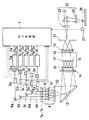
図1は、本発明のレーザプロセスとそれを用いたレーザアニール装置の基本構成を示す模式構成図である。レーザ発振器1a〜1eは、加工の際のスループットを安定して保持するために必要なレーザパワーを確保するため、複数台のレーザ発振器1a〜1eが並列に配置されている。各レーザ発振器1a〜1eはLD(レーザダイオード)(不図示)による励起であり、個々のレーザ発振器1a〜1eの励起光源となるLDへの印加電流は、電流モニタ2a〜2e(モニタリング機構)によりモニタリングされている。各レーザ発振器1a〜1eは、LD励起方式のNd:YVO4レーザのSHG出力であり、出力されるレーザビームは、可視光領域にあるとともに連続出力である。また、励起用LDがレーザ発振器1a〜1eの側ではなく電源(不図示)の側に設置され、かつ、励起エネルギは光ファイバ(不図示)を通じてレーザ発振器1a〜1eに伝送されている。また、各レーザ発振器1a〜1eの出射光軸上の前方には、それぞれ出力モニタ3a〜3eが配置されている。この出力モニタ3a〜3eと電流モニタ2a〜2eは、いずれも出力制御部4に接続されている。
FIG. 1 is a schematic configuration diagram showing a basic configuration of a laser process of the present invention and a laser annealing apparatus using the laser process. The laser oscillators 1a to 1e have a plurality of laser oscillators 1a to 1e arranged in parallel in order to ensure the laser power necessary to stably maintain the throughput during processing. Each of the laser oscillators 1a to 1e is excited by an LD (laser diode) (not shown), and currents applied to the LDs serving as excitation light sources of the individual laser oscillators 1a to 1e are
出力制御部4は、下記の(イ)〜(ハ)の機能をおこなうための制御アルゴリズムを備えている。(イ)通常は、出力制御部4は各レーザ発振器1a〜1eの出力が一定になるように、個々のレーザ発振器1a〜1eを励起用のLD電流の制御により制御している。(ロ)加工プロセスに必要な加工点のパワーを、加工点パワーモニタからデータを受け、予め定められている所定のパワーになるように、個々のレーザ発振器1a〜1eに対応した出力調整器(バリアブルアッテネータ)5a〜5eを同じ割合で調整する。(ハ)励起用のLDの寿命予測は、予め定められているデータにより行い、各レーザ発振器1a〜1eのメンテナンス時期を推定し、特定のレーザ発振器1a〜1eのLDが寿命に達したと判断した場合は、そのレーザ発振器1a〜1eのみの稼動を停止する。それによる全体の出力の低下分を残りのレーザ発振器1a〜1e全体で補完する。この補完のための動作は、稼動しているレーザ発振器1a〜1eに対応した、バリアブルアッテネータ5a〜5eの調整とLDの電流の調整により行う。この場合、後述するビーム合成光学系がホモジナイザの機能も果たしているので、仮に、レーザ発振器1a〜1eの内の1台が停止しても、加工点のエネルギ分布は変化しないので、パワーだけを補完すればよい。
The output control unit 4 includes a control algorithm for performing the following functions (a) to (c). (A) Normally, the output control unit 4 controls the individual laser oscillators 1a to 1e by controlling the LD current for excitation so that the outputs of the laser oscillators 1a to 1e are constant. (B) Output adjusters (corresponding to the individual laser oscillators 1a to 1e) so that the power of the machining points required for the machining process is received from the machining point power monitor and become a predetermined power. Variable attenuators) 5a to 5e are adjusted at the same rate. (C) Life prediction of the LD for excitation is performed based on predetermined data, the maintenance time of each laser oscillator 1a to 1e is estimated, and it is determined that the LD of the specific laser oscillator 1a to 1e has reached the life. In such a case, the operation of only the laser oscillators 1a to 1e is stopped. Thus, the entire decrease in output is supplemented by the entire remaining laser oscillators 1a to 1e. The operation for complementation is performed by adjusting the
各出力モニタ3a〜3eの各光軸上の前方には、個々のレーザ発振器1a〜1eの出力を制御する出力減衰器であるバリアブルアッテネータ5a〜5eが配設されている。このバリアブルアッテネータ5a〜5eの各光軸上の前方には反射ミラー6a〜6eを介して、ビーム偏向器7a〜7eとビーム合成光学系としてビーム合成器8が配置されている。なお、ビーム偏向器7a〜7eは、後述する高速シャッタおよび干渉縞対策の制御に使用される。ビーム合成器8は、順次、第一段のアレイレンズ9、第二段のアレイレンズ11および第一段のコンデンサレンズ12が配置されて構成されている。
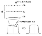
ビーム合成器8の光軸上の前方には、ミラー13を介して、順次、音響光学変調器(AOM)14からなる高速偏向回路とビームホモジナイザ15が配置されている。ビームホモジナイザ15は、順次、第三段のアレイレンズ16、第四段のアレイレンズ17、および、第二段のコンデンサレンズ18が配置されて構成されている。
In front of the
音響光学変調器14は、単結晶やガラス等の媒体中に超音波を発生させて周期的な屈折率変化を生じさせ、これにより位相型の回折格子を構成するもので、この音響光学変調器14にレーザ光が入射されると、回折光の強度や方向が、超音波の強度や周波数の状態によって変化するようになっている。この動作原理により、超音波の周波数に相当する量だけ、入射レーザ光の周波数がシフトする。この周波数シフト量は、任意に調整可能であり、入射レーザ光のそれぞれの強度は、超音波の出力を調整することで、0次光と1次回折光との比率を変えることができる。それらにより、レーザビームのスイッチング作用を光路途中で行うと共に、干渉縞の低減化のためにビームの方向を微小角で高速偏向させている。
The
これらの光学的な配置では、第一段のアレイレンズ9を通過したビームは第二段のアレイレンズ11および第一段のコンデンサレンズ12を通過した後、第三段のアレイレンズ16の開口部に結像される。結像されるということは、第一段のアレイレンズ9と第三段のアレイレンズ16の位置が第二段のアレイレンズ11と第一段のコンデンサレンズ12に対し、光学的には共役な位置関係にあることを意味している。
In these optical arrangements, the beam that has passed through the first-
ビームホモジナイザ15の光軸上の前方には、短軸用のシリンドリカルレンズ19が配置されている。また、シリンドリカルレンズ19の光軸上の前方には、ビームの周辺部をカットして整形する開孔が形成されているビーム整形アパチャ(矩形アパチャ)21が配置されている。
A short-
なお、光学的に第三段のアレイレンズ16を通過したビームは第四段のアレイレンズ17に入射し、さらに第二段のコンデンサレンズ18を介してビーム整形アパチャへと入射する。このとき第三段のアレイレンズ16位置とビーム整形アパチャは、第四段のアレイレンズ17と第二段のコンデンサレンズ18に対し、共役な位置関係にあるように設置される。つまり第三段のアレイレンズ16の像がビーム整形アパチャの21位置に結像されることを意味している。
The beam optically passing through the third
ビーム整形アパチャ21の光軸上の前方には結像光学系22が配置されている。この結像光学系22は、順次、コリメートレンズ23、スキャナ24、および、結像レンズ25が被加工物(不図示)を載置するテーブル26に対向して配置されて構成されている。また、結像レンズ25からの出射光に対しては、加工点出力モニタ27によりモニタリングを行っている。
An imaging
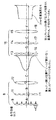
図2は、上述のレーザアニール装置の光学系における、ビーム合成系とホモジナイザによる作用の説明図である。なお、図2において各符号は、図1の符号を援用している。 FIG. 2 is an explanatory view of the operation of the beam synthesis system and the homogenizer in the optical system of the laser annealing apparatus described above. In addition, in FIG. 2, each code | symbol uses the code | symbol of FIG.
上述のように、第一段のアレイレンズ9を通過したビームは第二段のアレイレンズ11および第一段のコンデンサレンズ12を通過した後、第三段のアレイレンズ16の開口部に結像される。第一段のアレイレンズ9と第三段のアレイレンズ16位置が第二段のアレイレンズ11と第一段のコンデンサレンズ12に対し、共役な位置関係にある。
As described above, the beam that has passed through the first
また、第三段のアレイレンズ16を通過したビームは第四段のアレイレンズ17に入射し、さらに第二段のコンデンサレンズ18を介してビーム整形アパチャへと入射する。このとき第三段のアレイレンズ16位置とビーム整形アパチャは、第四段のアレイレンズ17と第二段のコンデンサレンズ18に対し、共役な位置関係にある。つまり第三段のアレイレンズ16の像がビーム整形アパチャ21の位置に結像される。図2において、各レンズの焦点距離と位置関係には、A=f1、C=f2、D=f4、F=f5の関係である。
Further, the beam that has passed through the third
ビーム整形アパチャ21の位置では、ほぼラインビームの形状に整形されているが、ここではより均一な部分を切り出しをおこなって分布の均一化とビームエッジ部のシャープさを確保する。ビーム整形アパチャ21を通過したビームはコリメートレンズ23と結像用レンズ25により、加工点に縮小して投影される。加工点でのラインビームは結像光学系22の光路途中に設置されたスキャナ24により走査される。
At the position of the
加工点での出力は、加工点出力モニタ27により検出され、検出結果は出力制御部4にフィードバッグされる。それにより、前述のバリアブルアッテネータ5a〜5eおよびLDの電流の制御により、加工点での出力が所定の出力となるように制御される。
The output at the machining point is detected by the machining point output monitor 27, and the detection result is fed back to the output control unit 4. Thus, the output at the processing point is controlled to be a predetermined output by controlling the currents of the
図2により、これらの光学系の配置と作用についてより詳しく説明すると、ビーム合成光学系8はアレイレンズから構成されおり、前述のように第一段のアレイレンズ9、第二段のアレイレンズ11、第一段のコンデンサレンズ12により第三段のアレイレンズ16に導かれる。ここまでのビーム合成光学系8の役目は第三段のアレイレンズ16開口に、個々のレーザ発振器1a〜1eから出力されるビームを重畳させて入射させることにある。
The arrangement and operation of these optical systems will be described in more detail with reference to FIG. 2. The beam combining
すなわち、図2に示すようにビーム合成光学系8により、第一段のアレイレンズ9での複数のビームを、重ねて第三段のアレアレンズ開口いっぱいに入射させる。一方、後段の第三段アレイレンズおよび第四段のアレイレンズ17、第二段のコンデンサレンズ18は第三段のアレイレンズ16の像をビーム整形アパチャ位置に結像させる。ここでもアレイレンズ像が重畳され、この作用によりビーム整形アパチャ21の位置でほぼ均一な強度分布を有するラインビームが得られる。
That is, as shown in FIG. 2, a plurality of beams from the first
ただし、後述するように固体レーザのSHG出力(Nd:YAGおよびNd:YVO4)を使用する場合は、重ね合わせによる干渉縞が発生するので、干渉縞対策が実施されていることが前提条件となる。 However, as will be described later, when using the SHG output (Nd: YAG and Nd: YVO 4 ) of the solid-state laser, interference fringes are generated due to superposition. Become.
このようなビーム合成光学系とビームホモジナイザ15による均一化光学系の組み合わせ方式を用いているので、たとえば、メンテナンスが必要なレーザ発振器1a〜1eの動作を停止した場合でも、加工点でのビーム形状、分布はほとんど変化しない。その結果、LDの劣化により交換作業が必要な場合、その発振器を装置から取り外してメンテナンス作業を進めるとともに、残りの発振器の出力を若干増加させることによって加工点パワーを確保することでメンテナンスによるライン停止時間を最小化することが可能になる。
Since such a combination system of the beam synthesizing optical system and the homogenizing optical system by the
なお、出力制御部4としては、どのレーザのLDが劣化傾向にあるかを出力モニタ3a〜3e値とLDの電流モニタ2a〜2eのモニタ値の経時変化を取得することで予測していく。
Note that the output control unit 4 predicts which laser LD is prone to deterioration by acquiring changes over time in the
レーザ発振器1a〜1eとしては、通常は励起用LDがレーザ発振器1a〜1eの筐体と一体化した構造をとっているが、外部にLDを設置し光ファイバーで励起光を伝送することにより、レーザ発振器1の取り外し作業を省き、アライメント変化を生じさせることなく、メンテナンスが可能となる。
The laser oscillators 1a to 1e usually have a structure in which the excitation LD is integrated with the housing of the laser oscillators 1a to 1e. However, by installing the LD outside and transmitting the excitation light through an optical fiber, Maintenance is possible without removing the
次に、ビームスキャニング方法およびスティープネスの確保について説明する。 Next, the beam scanning method and securing of the steepness will be described.
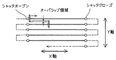
図3は、ビームスキャニングの概要を示す説明図である。ビームスキャニングの機構は2枚のミラーを直交するように配置し、それをガルバノメータスキャナで駆動する方式や、ポリゴンミラーを回転させる方式を用いることができる。 FIG. 3 is an explanatory diagram showing an outline of beam scanning. As the beam scanning mechanism, two mirrors are arranged so as to be orthogonal to each other, and a method of driving them with a galvanometer scanner or a method of rotating a polygon mirror can be used.
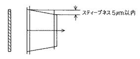
図3はガルバノメータスキャナによる方式を示しており、左右に走査を繰り返すことで、全面処理を行う。このときビームを一部オーバラップさせることにより、照射未処理の部分が生じないように設定する。従来の単純な集光系では特にビーム長軸方法のスティープネスが数百μmと大きいため、ビーム端部ではラテラル成長せずに、微結晶化する。よって走査領域全面をラテラル成長させることができないという課題を抱えていたが、本発明では、図4に説明図を示すように、長軸方向のスティープネスは、10μm以下の5μm以内であり、かつ、ラインビームを長さ方向にオーバラップさせながら被加工物である基板全面および一部分を結晶化していくことで、オーバラップ部分もラテラル成長することを見出した。スティープネスはできる限り小さいほうが良い。このスティープネスを確保するため、ビーム整形アパチャ21を結像する方式を開発した。ビーム裾部の立ち上がりLはおおよそエアリーディスクと同様になり、
L=1.22λ/NA
であらわすことができる。λは波長、NAは開口角である。よって開口角を大きく取ったほうが有利である。
FIG. 3 shows a system using a galvanometer scanner, and the entire surface processing is performed by repeating scanning left and right. At this time, the beam is partially overlapped so that an unirradiated portion is not generated. In the conventional simple focusing system, the beam long axis method has a large steepness of several hundreds μm, so that the crystal is crystallized without lateral growth at the beam end. Therefore, although there was a problem that the entire scanning region could not be laterally grown, in the present invention, as shown in the explanatory diagram of FIG. It has been found that the overlap portion also grows laterally by crystallizing the entire surface and a portion of the substrate as the workpiece while overlapping the line beams in the length direction. The steepness should be as small as possible. In order to ensure this steepness, a method for imaging the
L = 1.22λ / NA
Can be represented. λ is the wavelength and NA is the aperture angle. Therefore, it is advantageous to increase the opening angle.
次に、干渉縞対策および高速スイッチングについて説明する。 Next, interference fringe countermeasures and high-speed switching will be described.
加工点およびビーム整形アパチャ21の上では干渉縞が生じるため、結晶化のむらを生じる。この問題を解決するためレーザビームの光路途中に音響光学変調器14を設置し、図5にその状況説明図で示すように、個々に微小角で偏向する。これにより加工点での干渉縞の位置が変化し、そのスイッチング速度は通常10MHz程度までの応答性はある。CWラテラル成長でのプロセス時間は、Si膜を溶融させる50μsec程度は掛かるものであり、それでも数百回の干渉縞の移動が実現される。したがって、ビームホモジナイザ15を通過したレーザビームは、被加工物を照射する結晶化の時点では、均一加熱による均一した結晶化が期待できる。
Since interference fringes are generated on the processing point and the
以上に説明したように、本発明によれば、高品質のレーザアニールにより高品質の薄膜トランジスタの活性層の形成することができる。 As described above, according to the present invention, an active layer of a high quality thin film transistor can be formed by high quality laser annealing.
1a〜1e…レーザ発振器、2a〜2e…電流モニタ、3a〜3e…出力モニタ、4…出力制御部、8…ビーム合成器(ビーム合成光学系)、14…音響光学変調器、15…ビームホモジナイザ、21…ビーム整形アパチャ、22…結像光学系 DESCRIPTION OF SYMBOLS 1a-1e ... Laser oscillator, 2a-2e ... Current monitor, 3a-3e ... Output monitor, 4 ... Output control part, 8 ... Beam synthesizer (beam synthesis | combination optical system), 14 ... Acousto-optic modulator, 15 ... Beam homogenizer , 21 ... Beam shaping aperture, 22 ... Imaging optical system
Claims (8)
前記出力制御部は、前記各レーザ発振器の出力が一定になるよう、かつ、前記加工点のパワーが予め定められている所定のパワーになるように制御し、また、励起用のLDの寿命予測をおこなっていることを特徴とするレーザプロセス。 An optical system in which a plurality of laser oscillators by LD excitation are arranged in parallel, and the laser beam oscillated from each laser oscillator is synthesized and guided to a processing point in front of the output optical axis of each laser oscillator; This is a laser process in which a monitor for monitoring a laser beam is arranged, and a laser beam oscillated from each laser oscillator is controlled by an output control unit based on outputs from the monitor and a current monitor for monitoring the current of the LD. And
The output control unit controls the output of each laser oscillator to be constant and the power of the processing point to a predetermined power, and predicts the life of the excitation LD. A laser process characterized by
前記出力制御部は、前記モニタリング機構および前記出力モニタによりモニタした出力および励起用LD電流のデータから前記個々のレーザ発振器のメンテナンス時期を推定し、必要によってはメンテナンスが必要な前記レーザ発振器の稼動を停止させ、その分低下した必要パワーを他の前記レーザ発振器の出力を上昇させることで補完し、前記稼動を停止したレーザ発振器のメンテナンス時も装置全体の稼動が継続できる制御アルゴリズムを有していることを特徴とするレーザアニール装置。 A plurality of laser oscillators arranged in parallel and excited by LDs, and an output attenuator capable of varying individual laser outputs of the plurality of laser oscillators arranged sequentially in front of the output optical axis of each laser oscillator And a beam synthesis optical system that synthesizes the laser beam output from this output attenuator, and placed in front of the optical axis of this beam synthesis optical system to reduce interference fringes that occur when forming a line beam An acousto-optic modulator, a beam homogenizer comprising an array lens group and a condenser lens to form a uniform-distributed line beam from the laser beam output from the beam synthesis optical system, and a laser formed by the homogenizer A beam shaping aperture for reshaping the beam, an imaging optical system for imaging an image reshaped by the beam shaping aperture, A monitoring mechanism for detecting the output of the laser oscillator and the current of the LD for excitation, an output monitor for monitoring the output of the individual laser oscillators, and a processing point output monitor for monitoring the laser beam of the imaging optical system; An output control unit,
The output control unit estimates the maintenance time of each laser oscillator from the data monitored by the monitoring mechanism and the output monitor and the LD current for excitation, and if necessary, operates the laser oscillator that requires maintenance. It has a control algorithm that can be stopped and supplemented by increasing the output of the other laser oscillator by reducing the required power, and that the operation of the entire apparatus can be continued even during maintenance of the laser oscillator that has been stopped. A laser annealing apparatus characterized by that.
Priority Applications (1)
| Application Number | Priority Date | Filing Date | Title |
|---|---|---|---|
| JP2004106770A JP2005294493A (en) | 2004-03-31 | 2004-03-31 | Laser process and laser annealing equipment |
Applications Claiming Priority (1)
| Application Number | Priority Date | Filing Date | Title |
|---|---|---|---|
| JP2004106770A JP2005294493A (en) | 2004-03-31 | 2004-03-31 | Laser process and laser annealing equipment |
Publications (2)
| Publication Number | Publication Date |
|---|---|
| JP2005294493A true JP2005294493A (en) | 2005-10-20 |
| JP2005294493A5 JP2005294493A5 (en) | 2007-05-17 |
Family
ID=35327094
Family Applications (1)
| Application Number | Title | Priority Date | Filing Date |
|---|---|---|---|
| JP2004106770A Withdrawn JP2005294493A (en) | 2004-03-31 | 2004-03-31 | Laser process and laser annealing equipment |
Country Status (1)
| Country | Link |
|---|---|
| JP (1) | JP2005294493A (en) |
Cited By (9)
| Publication number | Priority date | Publication date | Assignee | Title |
|---|---|---|---|---|
| JP2008042032A (en) * | 2006-08-08 | 2008-02-21 | Sumitomo Heavy Ind Ltd | Stage driving method and laser processing apparatus using the method |
| JP2008147429A (en) * | 2006-12-11 | 2008-06-26 | Sumitomo Heavy Ind Ltd | Laser annealer and laser anneal method |
| JP2011510820A (en) * | 2008-02-07 | 2011-04-07 | カール ツァイス レーザー オプティックス ゲゼルシャフト ミット ベシュレンクテル ハフツング | Irradiation apparatus and method for controlling the energy of a laser light source |
| WO2015151177A1 (en) * | 2014-03-31 | 2015-10-08 | ギガフォトン株式会社 | Laser system or laser exposure system |
| WO2016006099A1 (en) * | 2014-07-11 | 2016-01-14 | ギガフォトン株式会社 | Laser system |
| DE102017104438A1 (en) | 2016-03-10 | 2017-09-14 | Fanuc Corporation | Machine learning apparatus, laser apparatus and machine learning method |
| DE102017108317A1 (en) | 2016-04-22 | 2017-10-26 | Fanuc Corporation | LASER DEVICE FOR CALCULATING EFFECTIVE RUNTIME |
| JP2018055103A (en) * | 2013-12-02 | 2018-04-05 | 株式会社半導体エネルギー研究所 | Processing device |
| US10092979B2 (en) | 2015-12-25 | 2018-10-09 | Gigaphoton Inc. | Laser irradiation apparatus |
-
2004
- 2004-03-31 JP JP2004106770A patent/JP2005294493A/en not_active Withdrawn
Cited By (28)
| Publication number | Priority date | Publication date | Assignee | Title |
|---|---|---|---|---|
| JP2008042032A (en) * | 2006-08-08 | 2008-02-21 | Sumitomo Heavy Ind Ltd | Stage driving method and laser processing apparatus using the method |
| JP2008147429A (en) * | 2006-12-11 | 2008-06-26 | Sumitomo Heavy Ind Ltd | Laser annealer and laser anneal method |
| JP2011510820A (en) * | 2008-02-07 | 2011-04-07 | カール ツァイス レーザー オプティックス ゲゼルシャフト ミット ベシュレンクテル ハフツング | Irradiation apparatus and method for controlling the energy of a laser light source |
| US10854697B2 (en) | 2013-12-02 | 2020-12-01 | Semiconductor Energy Laboratory Co., Ltd. | Display device and method for manufacturing the same |
| US10312315B2 (en) | 2013-12-02 | 2019-06-04 | Semiconductor Energy Laboratory Co., Ltd. | Display device and method for manufacturing the same |
| US12048207B2 (en) | 2013-12-02 | 2024-07-23 | Semiconductor Energy Laboratory Co., Ltd. | Display device and method for manufacturing the same |
| US11672148B2 (en) | 2013-12-02 | 2023-06-06 | Semiconductor Energy Laboratory Co., Ltd. | Display device and method for manufacturing the same |
| US11004925B2 (en) | 2013-12-02 | 2021-05-11 | Semiconductor Energy Laboratory Co., Ltd. | Display device and method for manufacturing the same |
| US10879331B2 (en) | 2013-12-02 | 2020-12-29 | Semiconductor Energy Laboratory Co., Ltd. | Display device and method for manufacturing the same |
| US10872947B2 (en) | 2013-12-02 | 2020-12-22 | Semiconductor Energy Laboratory Co., Ltd. | Display device and method for manufacturing the same |
| JP2018055103A (en) * | 2013-12-02 | 2018-04-05 | 株式会社半導体エネルギー研究所 | Processing device |
| US10763322B2 (en) | 2013-12-02 | 2020-09-01 | Semiconductor Energy Laboratory Co., Ltd. | Display device and method for manufacturing the same |
| CN110047760A (en) * | 2013-12-02 | 2019-07-23 | 株式会社半导体能源研究所 | Display device and its manufacturing method |
| US10355067B2 (en) | 2013-12-02 | 2019-07-16 | Semiconductor Energy Laboratory Co., Ltd. | Display device and method for manufacturing the same |
| JP2019023739A (en) * | 2013-12-02 | 2019-02-14 | 株式会社半導体エネルギー研究所 | apparatus |
| US10495890B2 (en) | 2014-03-31 | 2019-12-03 | Gigaphoton Inc. | Laser system or laser exposure system |
| JPWO2015151177A1 (en) * | 2014-03-31 | 2017-04-13 | ギガフォトン株式会社 | Laser system or laser exposure system |
| WO2015151177A1 (en) * | 2014-03-31 | 2015-10-08 | ギガフォトン株式会社 | Laser system or laser exposure system |
| US10050408B2 (en) | 2014-07-11 | 2018-08-14 | Gigaphoton Inc. | Laser system |
| KR102245053B1 (en) * | 2014-07-11 | 2021-04-26 | 기가포톤 가부시키가이샤 | Laser system |
| JPWO2016006099A1 (en) * | 2014-07-11 | 2017-04-27 | ギガフォトン株式会社 | Laser system |
| WO2016006099A1 (en) * | 2014-07-11 | 2016-01-14 | ギガフォトン株式会社 | Laser system |
| KR20170030483A (en) * | 2014-07-11 | 2017-03-17 | 기가포톤 가부시키가이샤 | Laser system |
| US10092979B2 (en) | 2015-12-25 | 2018-10-09 | Gigaphoton Inc. | Laser irradiation apparatus |
| US10242325B2 (en) | 2016-03-10 | 2019-03-26 | Fanuc Corporation | Machine learning apparatus, laser apparatus and machine learning method |
| DE102017104438A1 (en) | 2016-03-10 | 2017-09-14 | Fanuc Corporation | Machine learning apparatus, laser apparatus and machine learning method |
| US10033150B2 (en) | 2016-04-22 | 2018-07-24 | Fanuc Corporation | Laser apparatus for calculating effective driving time |
| DE102017108317A1 (en) | 2016-04-22 | 2017-10-26 | Fanuc Corporation | LASER DEVICE FOR CALCULATING EFFECTIVE RUNTIME |
Similar Documents
| Publication | Publication Date | Title |
|---|---|---|
| JP3860444B2 (en) | Silicon crystallization method and laser annealing equipment | |
| JP4567984B2 (en) | Flat panel display manufacturing equipment | |
| KR101371265B1 (en) | Laser irradiation apparatus, laser irradiation method and manufacturing method of semiconductor device | |
| US7365285B2 (en) | Laser annealing method and apparatus | |
| KR101017848B1 (en) | Beam homogenizer and laser irradiation device and semiconductor device manufacturing method | |
| KR100894512B1 (en) | Crystallization apparatus and crystallization method | |
| JP5133158B2 (en) | Multiple beam laser equipment | |
| JP4408668B2 (en) | Thin film semiconductor manufacturing method and manufacturing apparatus | |
| KR20020016585A (en) | Semiconductor device, manufacturing method therefor, and semiconductor manufacturing apparatus | |
| JPH08148423A (en) | Laser annealing method | |
| JP2005294493A (en) | Laser process and laser annealing equipment | |
| KR20050119132A (en) | Laser processing apparatus and laser processing method | |
| US20040241923A1 (en) | Laser annealing apparatus and laser annealing method | |
| JP4772261B2 (en) | Display device substrate manufacturing method and crystallization apparatus | |
| JP2005294493A5 (en) | ||
| US7724785B2 (en) | Multiple pulsed-laser system for silicon crystallization | |
| JP2006156676A (en) | Laser anneal method | |
| JP4908269B2 (en) | Laser irradiation method and apparatus | |
| JP2013089930A (en) | Laser annealing method and laser annealing apparatus | |
| KR102923167B1 (en) | Laser annealing device and laser annealing method | |
| JP5137388B2 (en) | Laser irradiation apparatus, laser irradiation method, and manufacturing method of semiconductor device | |
| JP2007273833A (en) | Semiconductor film crystallization apparatus and crystallization method | |
| JP5068972B2 (en) | Laser annealing apparatus, semiconductor film substrate, element substrate, and electro-optical device | |
| KR20130112112A (en) | Method of generating laser having variable pulse width and method of generating high power laser | |
| KR100814821B1 (en) | Crystallization Apparatus and Method of Silicon Thin Film |
Legal Events
| Date | Code | Title | Description |
|---|---|---|---|
| A521 | Written amendment |
Effective date: 20070326 Free format text: JAPANESE INTERMEDIATE CODE: A523 |
|
| A621 | Written request for application examination |
Effective date: 20070326 Free format text: JAPANESE INTERMEDIATE CODE: A621 |
|
| RD04 | Notification of resignation of power of attorney |
Effective date: 20070424 Free format text: JAPANESE INTERMEDIATE CODE: A7424 |
|
| A761 | Written withdrawal of application |
Free format text: JAPANESE INTERMEDIATE CODE: A761 Effective date: 20091019 |