JP2005294473A - Exposure apparatus, device manufacturing method, and device - Google Patents
Exposure apparatus, device manufacturing method, and device Download PDFInfo
- Publication number
- JP2005294473A JP2005294473A JP2004106358A JP2004106358A JP2005294473A JP 2005294473 A JP2005294473 A JP 2005294473A JP 2004106358 A JP2004106358 A JP 2004106358A JP 2004106358 A JP2004106358 A JP 2004106358A JP 2005294473 A JP2005294473 A JP 2005294473A
- Authority
- JP
- Japan
- Prior art keywords
- lot
- wafer
- unit
- processing
- exposure apparatus
- Prior art date
- Legal status (The legal status is an assumption and is not a legal conclusion. Google has not performed a legal analysis and makes no representation as to the accuracy of the status listed.)
- Withdrawn
Links
Images
Classifications
-
- G—PHYSICS
- G03—PHOTOGRAPHY; CINEMATOGRAPHY; ANALOGOUS TECHNIQUES USING WAVES OTHER THAN OPTICAL WAVES; ELECTROGRAPHY; HOLOGRAPHY
- G03F—PHOTOMECHANICAL PRODUCTION OF TEXTURED OR PATTERNED SURFACES, e.g. FOR PRINTING, FOR PROCESSING OF SEMICONDUCTOR DEVICES; MATERIALS THEREFOR; ORIGINALS THEREFOR; APPARATUS SPECIALLY ADAPTED THEREFOR
- G03F7/00—Photomechanical, e.g. photolithographic, production of textured or patterned surfaces, e.g. printing surfaces; Materials therefor, e.g. comprising photoresists; Apparatus specially adapted therefor
- G03F7/70—Microphotolithographic exposure; Apparatus therefor
- G03F7/70483—Information management; Active and passive control; Testing; Wafer monitoring, e.g. pattern monitoring
- G03F7/70491—Information management, e.g. software; Active and passive control, e.g. details of controlling exposure processes or exposure tool monitoring processes
- G03F7/70533—Controlling abnormal operating mode, e.g. taking account of waiting time, decision to rework or rework flow
Landscapes
- Physics & Mathematics (AREA)
- General Physics & Mathematics (AREA)
- Exposure And Positioning Against Photoresist Photosensitive Materials (AREA)
- Exposure Of Semiconductors, Excluding Electron Or Ion Beam Exposure (AREA)
Abstract
【課題】 ロットの切換えによって生じる時間損失を抑えること。
【解決手段】 複数のユニットを有する露光装置100は、各ロットに関して処理工程を計画する計画手段と、前記計画手段により計画された、連続して処理されるべき第1及び第2のロットに関する処理工程を結合する結合手段と、前記結合手段により結合された処理工程に基づいて、前記複数のユニットを制御する制御手段とを有する。前記結合手段は、前記第1ロットの処理の完了前且つ前記第2ロットの搬入前に、前記第1ロットに関し使用されなくなったユニットが前記第2ロットに関する第1の処理を開始するように、前記処理工程を結合する。
【選択図】 図1
To suppress time loss caused by lot switching.
An exposure apparatus having a plurality of units includes a planning unit for planning a processing process for each lot, and a process for first and second lots to be processed in succession planned by the planning unit. A coupling unit that couples the processes; and a control unit that controls the plurality of units based on the processing steps coupled by the coupling unit. The combining means is configured so that a unit that is no longer used for the first lot starts the first processing for the second lot before the processing of the first lot is completed and before the second lot is carried in, Combine the processing steps.
[Selection] Figure 1
Description
本発明は、複数のユニットを有する露光装置、デバイス製造方法及びデバイスに関する。 The present invention relates to an exposure apparatus having a plurality of units, a device manufacturing method, and a device.
従来、半導体デバイス生産の主流は、DRAMなどの単一製品(単一ロット)を大量生産する形式であった。そのため、投影露光装置は、単一ロットを連続して繰り返し処理することが多く、長期間にわたり連続運転し続ける場合が多かった。 Conventionally, the mainstream of semiconductor device production has been a form of mass production of a single product (single lot) such as DRAM. For this reason, the projection exposure apparatus often repeatedly processes a single lot continuously, and often continues to operate continuously for a long period of time.
しかし、近年では、ASICなどの特注LSI製品を多品種小ロット型で生産する場合が増えており、一つの投影露光装置で製造するロットを短期間で変更する場合が多くなっている。このような状況において、連続したロットを効率良く処理する運転制御方式が望まれている。このような運転制御方式として、生産予定のロットの制御情報を予約しておき、現在処理中のロットの製造が完了したときに、予約された制御情報に基づいて、次のロットの処理を自動で開始するバッチ処理技術が知られている。 However, in recent years, the number of custom-made LSI products such as ASICs produced in a variety of small lots has increased, and lots manufactured with a single projection exposure apparatus are often changed in a short period of time. In such a situation, an operation control system that efficiently processes continuous lots is desired. As such an operation control method, the control information of the lot to be produced is reserved, and when the production of the currently processed lot is completed, the processing of the next lot is automatically performed based on the reserved control information. Batch processing techniques starting with are known.
特許文献1では、現在処理中のロットの処理が完了する前に、次のロットのレシピ(制御情報)の存否に応じて、次のロットを製造するための基板を事前にウエハ準備完了位置へ搬送し、また、ロット処理に必要な露光装置の資源のオン/オフ状態を制御して、ロットの切換えの際に生じる時間損失を抑える方法が、本出願人により開示されている。
しかしながら、特許文献1では、次のロットの基板をウエハ準備完了位置へ搬送した後に、縮小投影レンズの結像面(焦点面)に基板(ウエハ)面を合致させるフォーカスの精度や投影されるパターンを被投影領域に正確に重ね合わせるアライメントの精度を高精度に維持するために、製品(ロット)切換えの際に、基板の露光前に調整可能な補正パラメータを予め自動計測し、組織化された構成部品(ユニット)のパラメータを適正値に設定する各種装置の補正処理が行われるため、露光を行うまでに時間がかかる。
However, in
特に、近年の微細化デバイスへ対応するためには、これらの補正パラメータをより精密に計測する必要があるため、補正パラメータの計測時間は更に長くなり、補正パラメータの種類も一層増える傾向にある。したがって、前述した多品種小ロット型での製造が増える状況において、製品(ロット)を切換える際の補正パラメータ計測に要する時間が増大するため、この観点からも効率的な処理が望まれる。 In particular, in order to cope with recent miniaturized devices, it is necessary to measure these correction parameters more precisely. Therefore, the measurement time of the correction parameters becomes longer and the types of correction parameters tend to increase further. Therefore, since the time required for measuring the correction parameter when switching the product (lot) increases in the situation where the production of the above-described multi-product small lot type increases, an efficient process is desired also from this viewpoint.
また、パターンを形成した原版(レチクル)の位置決め、パルスレーザー光源のガス交換、レーザー光波長較正の実施、ウエハ位置合わせスコープの計測光の光量調整、マスクパターンの解像を最適にする照明条件設定等の各ユニットにおける前工程がロットの切換毎に行われるため、これらの処理に起因する時間損失が製品(ロット)切換え頻度の増加に伴って増大するという問題がある。 In addition, positioning of the original plate (reticle) on which the pattern is formed, gas exchange of the pulse laser light source, laser light wavelength calibration, adjustment of the amount of measurement light from the wafer alignment scope, and setting of illumination conditions that optimize mask pattern resolution Therefore, there is a problem that time loss due to these processes increases with an increase in the frequency of product (lot) switching.
本発明は上記の背景に鑑みてなされたものであり、ロットの切換えによって生じる時間損失を抑えることを目的とする。 The present invention has been made in view of the above background, and an object thereof is to suppress time loss caused by lot switching.
本発明の第1の側面は、複数のユニットを有する露光装置に係り、各ロットに関して処理工程を計画する計画手段と、前記計画手段により計画された、連続して処理されるべき第1及び第2のロットに関する処理工程を結合する結合手段と、前記結合手段により結合された処理工程に基づいて、前記複数のユニットを制御する制御手段とを有し、前記結合手段は、前記第1ロットの処理の完了前且つ前記第2ロットの搬入前に、前記第1ロットに関し使用されなくなったユニットが前記第2ロットに関する第1の処理を開始するように、前記処理工程を結合することを特徴とする。 According to a first aspect of the present invention, there is provided an exposure apparatus having a plurality of units, a planning means for planning a processing process for each lot, and a first and a first to be processed successively planned by the planning means. A combining means for combining the processing steps related to the two lots, and a control means for controlling the plurality of units based on the processing steps combined by the combining means. The processing steps are combined so that a unit that is no longer used for the first lot starts the first processing for the second lot before the completion of processing and before the second lot is brought in. To do.
本発明の第2の側面は、デバイス製造方法に係り、上記の露光装置を用いて基板にパターンを露光する露光工程を含むことを特徴とする。 A second aspect of the present invention relates to a device manufacturing method and includes an exposure step of exposing a pattern to a substrate using the exposure apparatus described above.
本発明の第3の側面は、デバイス製造方法に係り、複数のユニットを有する露光装置を用いてデバイスを製造するデバイス製造方法であって、各ロットに関して処理工程を計画する計画段階と、前記計画段階において計画された、連続して処理されるべき第1及び第2のロットに関する処理工程を結合する結合段階と、前記結合段階において結合された処理工程に基づいて、前記複数のユニットを制御する制御段階とを含み、前記結合段階において、前記露光装置による前記第1ロットの処理の完了前且つ前記露光装置への前記第2ロットの搬入前に、前記第1ロットに関し使用されなくなったユニットが前記第2ロットに関する第1の処理を開始するように、前記処理工程を結合することを特徴とする。 A third aspect of the present invention relates to a device manufacturing method, which is a device manufacturing method for manufacturing a device using an exposure apparatus having a plurality of units, the planning step of planning a processing process for each lot, and the plan The plurality of units are controlled based on a combination step that combines the processing steps for the first and second lots to be processed in succession planned in the step, and the processing steps combined in the combination step. A unit that is no longer used for the first lot before the completion of the processing of the first lot by the exposure apparatus and before the second lot is transferred to the exposure apparatus in the combining stage. The processing steps are combined so as to start the first processing relating to the second lot.
本発明の第4の側面は、デバイスに係り、上記のデバイス製造方法により製造されたことを特徴とする。 A fourth aspect of the present invention relates to a device and is characterized by being manufactured by the above-described device manufacturing method.
本発明によれば、ロットの切換えによって生じる時間損失を抑えることができる。 According to the present invention, time loss caused by lot switching can be suppressed.
[実施形態1]
図1は、本発明の実施形態に係るシングルステージ型露光装置100の概略構成を示す。図1において、パルスレーザー光源101には、例えばKrF等のガスが封入され、レーザー光を発光する。パルスレーザー光源101は、遠紫外領域の波長248nmの光を発光する。また、パルスレーザー光源101には、共振器を構成するフロントミラー、露光波長を狭帯化するための回折格子、プリズム等からなる狭帯化モジュール、波長の安定性やスペクトル幅をモニタするための分光器やディテクタ等からなるモニタモジュール、及びシャッター等が設けられている。レーザー制御装置102は、レーザー光源101のガス交換動作、波長安定化動作、放電印加電圧等を制御する。本実施形態では、レーザー制御装置102による単独制御は行わず、インタフェースケーブルで接続した露光装置100全体の主制御装置103からの命令によって制御する例を示しているが、本発明はこれに限定されない。
[Embodiment 1]
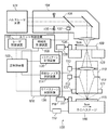
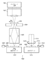
FIG. 1 shows a schematic configuration of a single stage
パルスレーザー光源101から射出されたビームは、照明光学系104のビーム整形光学系(不図示)を通して所定のビーム形状に整形された後、オプティカルインテグレータ(不図示)に入射されて、後述するマスク109を均一な照度分布で照明するために、多数の2次光源を形成する。照明光学系104の開口絞り105の開口部の形状は、略円形であり、照明系制御装置108によってその開口部の直径や照明光学系の開口数(NA)を所望の値に設定することができる。この場合、後述する縮小投影レンズ110の開口数に対する照明光学系104の開口数の比の値が、コヒーレンスファクタ(σ値)となるため、照明系制御装置108は、照明光学系104の開口絞り105を制御することによってσ値を設定することができる。照明光学系104の光路上には、ハーフミラー106が配置され、マスク109に照明される露光光の一部がハーフミラー106によって反射され取り出される。ハーフミラー106の反射光の光路上には、紫外光用のフォトセンサ107が配置され、露光光の強度(露光エネルギー)に対応した出力を発生する。フォトセンサ107の出力は、パルスレーザー光源101のパルス発光毎に積分を行う積分回路(不図示)によって、1パルスあたりの露光エネルギーに変換され、照明系制御装置108を介して露光装置100本体を制御する主制御装置103に入力される。
A beam emitted from the pulse
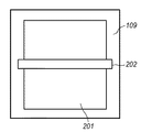
レチクル(又はマスク)109には、焼き付けが行われる半導体素子の回路パターンが形成されており、照明光学系104によって露光光が照射される。可変ブラインド(不図示)は、光軸に直交する面上に遮光板を配置し、マスク109の回路パターン面の照射領域を任意に設定することができる。図2は、マスク109に露光光が照明されている状態を示す。マスク109の回路パターン201の一部は、スリット状光束202によってスリット照明されており、図1に示す投影レンズ110によってフォトレジストが塗布されたウエハ115上に、回路パターン201の一部が縮小倍率β(例えば、βは1/4)で縮小露光される。図1において矢印(Scan)で示すように、マスク109及びウエハ115を、投影レンズ110及びスリット状光束202に対し、投影レンズ110の縮小比率βと同じ速度比率で互いに逆方向にスキャンさせながらパルスレーザー光源101からのパルス発光によるパルス露光を繰り返すことによって、マスク109全面の回路パターン201をウエハ115上の1チップ領域又は複数チップ領域に転写することができる。
On the reticle (or mask) 109, a circuit pattern of a semiconductor element to be baked is formed, and the illumination
投影レンズ110の瞳面(レチクルに対するフーリエ変換面)上には、開口部が略円形である投影レンズの開口絞り111が配置され、モータ等の駆動手段112を用いて開口部の直径を制御することによって、投影レンズの開口数(NA)が所望の値に設定されうる。また、フィールドレンズ駆動装置113は、投影レンズ110中のレンズ系の一部を構成するフィールドレンズを、空気圧や圧電素子などを利用して投影レンズの光軸上に移動させるものであり、投影レンズの諸収差の悪化を防止しつつ、投影倍率や歪曲誤差を良好にすることができる。
On the pupil plane of the projection lens 110 (Fourier transform plane with respect to the reticle), an
ウエハステージ116は、3次元方向に移動可能であり、投影レンズ110の光軸方向(Z方向)及びこの方向に直交する面内(X-Y面)を移動することができる。ウエハステージに固定された移動鏡117までの距離を、レーザー干渉計118で計測することによって、ウエハステージ116のX-Y面位置が検出される。露光装置100の主制御装置103の制御下にあるウエハステージ制御装置120は、レーザー干渉計118によってウエハステージ116の位置を検出し、モータ等の駆動手段119を制御することによって、ウエハステージ116を所定のX-Y面位置へ移動させる。また、フォーカス面検出手段121及び122は、ウエハ115上のフォトレジストを感光させない非露光光から成る複数個の光束を投光光学系121から投光し、ウエハ115上に各々集光されて反射された光束を検出光学系122で検出することによって、フォーカス面を検出する。図示は省略したが、検出光学系122内には、各反射光束に対応させて複数個の位置検出用の受光素子が配置されており、各位置検出用受光素子の受光面とウエハ115上での各光束の反射点が結像光学系によって略共役となるように構成されている。投影レンズ110の光軸方向におけるウエハ面の位置ずれは、検出光学系122内の位置検出用受光素子上の入射光束位置ずれとして計測される。
The
本実施形態では、マスク109とウエハ115とが所定の関係となるように位置決めした後、主制御装置103からの同期信号に基づいて、レーザー制御装置102、ウエハステージ制御装置120及びマスクステージ制御装置126が、マスク202全面の回路パターン201をウエハ115のチップ領域へ転写するスキャン露光を行う。その後、ウエハステージ116によってウエハ115を所定量X−Y平面内に駆動させ、ウエハ115の他の領域を順次同じように投影露光するステップ・アンド・スキャン方式の露光処理が実行される。
In the present embodiment, after positioning the
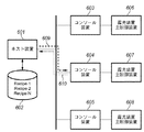
図6は、露光装置を使用した半導体製造工程で用いられる装置構成の一例を示す。図6において、複数の投影露光装置を管理する上位ホスト装置601には、ハードディスクドライブ602が接続される。ハードディスクドライブ602は、製品に応じて露光処理条件が詳細に設定されたレシピ(制御情報)を保持するデータベースを含む。露光装置の主制御装置606、607、608は、図1に示した露光装置100の主制御装置103にそれぞれ対応する。コンソール装置603、604、605は、露光装置100に付属するユーザインターフェースを持つ。コンソール装置603、604、605は、主制御装置606、607、608と1対1に接続される。オペレータは、個々のコンソール装置603、604、605を介して露光装置の各ユニットを制御することができる。ホスト装置601と各主制御装置606、607、608とは、付属するコンソール装置603、604、605を介して、ネットワーク通信機構によってオンライン接続され、ホスト装置601からの集中的な装置制御も可能である。本実施形態では、後者のホスト装置601を介したオンライン装置制御を一例として説明するが、本発明はこれに限定されない。
FIG. 6 shows an example of an apparatus configuration used in a semiconductor manufacturing process using an exposure apparatus. In FIG. 6, a
オンライン通信609は、ホスト装置601から各コンソール装置603、604、605へ転送される製品ロットの処理要求を示し、製品ロットの露光処理を露光装置へ予約するときのデータの流れを示す。オンライン通信610は、各露光装置の主制御装置606、607、608の稼動状態及び前述のロット処理予約状態をホスト装置601へ通知するときのデータの流れを示す。ホスト装置601は、これらのオンライン通信によって露光装置を集中的に制御する。
The
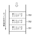
製品ロットを露光処理する場合、オペレータは、製品の種類に応じたレシピをホスト装置601で作成し、レシピ名称(例えば、Recipe-1、Recipe-2、…、Recipe-N)を付けて、レシピデータベース602へ保存する。製品を露光装置で生産する準備が整うと、レシピデータベース602から保存した製品のレシピ名称を選択した後、使用する露光装置(不図示)を指定する。ホスト装置601は、指定された露光装置の主制御装置(図6では主制御装置607)に接続されたコンソール装置(図6ではコンソール装置604)へ、ブロードバンド方式のオンライン通信609を介してレシピデータを転送する。レシピデータを受信したコンソール装置604は、図7に示したロット待ち行列の最後にレシピデータを挿入する。図7の場合、ロット要求701、702、703の順番にレシピデータが格納されている。露光装置は、ロット待ち行列として格納されたレシピデータが無くなるまで、順次露光処理を実行する。
When exposing a product lot, the operator creates a recipe corresponding to the type of product on the
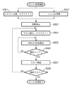
次に、図3を用いて単一ロットを処理する場合に、露光装置100において実行される一連の工程を概略的に示すフローチャートであり。ステップS301〜ステップS303の工程は、次のロットにおける最初のウエハ115を搬送する前に実行される前工程に相当する。露光装置100は、ロット処理が開始されると、最初にステップS301とステップS302の並行動作を開始する。
FIG. 4 is a flowchart schematically showing a series of steps executed in the
ステップS301では、ロット生産に用いるマスク109をマスクハンド(不図示)によってマスクステージ123へ搬送し、マスク位置合わせスコープ(不図示)を用いてマスク109とマスクステージ123の相対位置を観察しながら、マスクステージ123を位置決めする。
In step S301, the
ステップS302では、ステップS301と並行処理が可能な構成部品(ユニット)の前準備を行う。例えば、パルスレーザー光源101のガス交換、レーザー光波長較正の実施、ウエハ位置合わせスコープ(不図示)の計測光の光量調整、マスクパターンの解像を最適にする照明条件設定等を並行処理する。この照明条件設定では、投影レンズ110の開口数(NA)や照明光学系のコヒーレンスファクタ(σ値)105が指定条件に合うように制御される。ステップS301とステップS302のユニット制御が終了すると、ステップS303に進む。
In step S302, preparation is made for a component (unit) that can be processed in parallel with step S301. For example, parallel processing includes gas exchange of the pulse
ステップS303では、ウエハ115の加工精度を維持するために装置補正処理を実施する。代表的な装置補正処理の一つは、投影レンズ110を通した光で焦点面を計測するスルーザレンズオートフォーカスシステム(TTLAF)(不図示)による処理である。これは、露光熱等によって投影レンズ110の焦点面が設計位置から変動する量を計測し、焦点面とウエハ面を合致させるように像面補正する処理である。
In step S303, an apparatus correction process is performed to maintain the processing accuracy of the
ステップS304では、ウエハハンド(不図示)によってウエハ115をウエハステージ116へ搬入し、ウエハ位置合わせスコープ(不図示)でウエハ115上のアライメントマークを観察しながら、マスク109とウエハ115の相対位置決めを行う。
In step S304, the
ステップS305では、ウエハステージ116をチップ露光開始位置へ所定量X-Y平面内にステップ駆動させた後、マスクステージ123とウエハステージ115を同期走査しながら、パルスレーザー光源101によってスキャン露光を実施する。次のロットの基板を搬送する前に、ステップS301〜ステップS303の前工程が終了しているため、次のロットの基板を搬入した後に、直ちにスキャン露光を開始することができる。
In step S305, after the
ステップS306では、ウエハの全チップの露光が終了し、最終チップの露光が終了したか否かを判定する。最終チップの露光が終了した場合には(ステップS306で「Yes」)、ステップS307に進み、最終チップの露光が終了していない場合には(ステップS306で「No」)、ステップS305へ戻る。 In step S306, it is determined whether the exposure of all the chips on the wafer has been completed and the exposure of the final chip has been completed. If the exposure of the final chip is completed (“Yes” in step S306), the process proceeds to step S307. If the exposure of the final chip is not completed (“No” in step S306), the process returns to step S305.
ステップS307では、ウエハハンド(不図示)によってウエハを搬出する。 In step S307, the wafer is unloaded by a wafer hand (not shown).
ステップS308では、ロットの全ウエハの露光が終了し、最終ウエハの露光が終了したか否かを判定する。最終ウエハの露光が終了した場合には(ステップS308で「Yes」)ロット処理を終了し、最終ウエハの露光が終了していない場合には(ステップS308で「No」)、ウエハ搬入ステップS304へ戻り、最終ウエハの露光が終了するまでステップS304からステップS308までの処理を繰り返す。 In step S308, it is determined whether exposure of all wafers in the lot has been completed and exposure of the final wafer has been completed. If the exposure of the final wafer is completed (“Yes” in step S308), the lot processing is completed. If the exposure of the final wafer is not completed (“No” in step S308), the process proceeds to wafer loading step S304. The process from step S304 to step S308 is repeated until the exposure of the final wafer is completed.
以上、説明したステップS301からステップS308までの各工程は、単一のユニット又は複数ユニットの動作の組合せによって実行されうる。 As described above, each step from step S301 to step S308 described above can be executed by a single unit or a combination of operations of a plurality of units.
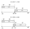
図4(a)は、従来のバッチ処理技術を用いて、単一ロットAと単一ロットBを2ロット連続して実行した場合のタイムチャートである。ロットAは時間405で開始して時間406で終了する。ロットAをロットBに切換えた後、時間407からロットBが開始される。401と403は、図3の露光装置100において実行される一連の基本工程に示した、ステップS301〜ステップS303のロット準備処理に対応する。402と404は、図3のステップS304からステップS308までの基板の搬入から搬出までの処理に対応する。このように、従来の露光処理では、ロットAからロットBに切換えるときに、時間406から時間407までの間の時間損失が生じ、ロットAからロットBに連続的に切換えることができなかった。これに対し、本発明の好適な実施形態では、ロットAの露光処理が終了する406より前に、次に続くロットBを開始414するため、ロットAからロットBに連続的に切換えることができ、図4(b)に示すように、ロットBを先行処理させることによって、ロット切換え時に生じる時間損失を抑えることができる。
FIG. 4A is a time chart in the case where a single lot A and a single lot B are successively executed using a conventional batch processing technique. Lot A starts at
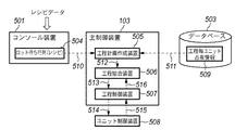
次に、本発明の最も特徴的な方法の一つである、先行ロットで制御するユニットが空いた時に、ロット終了を待たずに後方ロットの先行工程を開始する工程順序計画方法と、この工程順序計画に基づいて運転制御する方法について説明する。図5は、本発明の好適な実施の形態に係るシステムの構成を示す概略図である。本システムは、前述したコンソール装置501、主制御装置103、及び露光装置100のロット処理工程表を格納するデータベース503で構成される。コンソール装置501は、ホスト装置から送信されるレシピデータをロット待ち行列(レシピ)504へ格納すると共に、主制御装置103の工程計画装置505へ送信する(510)。計画手段としての工程計画装置505は、レシピデータに設定されている例えばウエハ処理枚数や照明条件等の露光条件と、予めデータベースに保存された、露光処理の工程毎に占有される構成部品(ユニット)を示す情報(工程毎ユニット占有情報)509とに基づいて(511)、露光処理の工程順序を示す工程順序計画情報を作成することによって、各ロットに関して処理工程を計画する(512)。
Next, one of the most characteristic methods of the present invention is a process sequence planning method for starting a preceding process of a rear lot without waiting for the end of the lot when a unit controlled by the preceding lot becomes available, and this process. A method for controlling the operation based on the sequence plan will be described. FIG. 5 is a schematic diagram showing the configuration of a system according to a preferred embodiment of the present invention. This system includes a
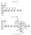
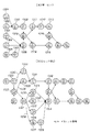
図9(a)は、工程計画装置505が作成する単一ロットの工程順序計画情報を有向グラフで例示した図である。円で記したノードは露光装置100の工程名を示し、矢印で記した枝は各工程の実行順序を示す。入力矢印の無いノードは、いつでも処理可能な状態にあることを意味する。また、工程901、903、904、905は、並行処理が可能である。入力矢印が有るノード、例えば工程906は、前工程である902、903、904、905が全て終了し、入力矢印が無くなった時が開始条件となる。
FIG. 9A is a diagram illustrating the process sequence plan information of a single lot created by the
図9(a)は、図3で説明した単一ロットの処理フローでN枚のウエハを露光した時の工程順序計画情報であり、図3と比べながら説明する。ステップS301のレチクル交換及びアライメントは、レチクル交換工程901及びレチクルアライメント902の2工程に相当する。ステップS302のロット前準備は、スコープ調光903、照明条件設定904及びレーザー波長較正905の3工程に相当する。ステップS303の装置補正は、TTLAF補正工程906に相当する。ロット処理が開始すると、レチクル交換工程901、ウエハ位置合わせスコープ調光工程903、照明条件設定工程904及びレーザー波長較正工程905を同時に開始することができる。これは、各工程を実施する時に占有するユニットが重複しないからである。レチクル交換工程901が終了すると、レチクルアライメント工程902が開始される。TTLAF補正工程906は、レチクルアライメント工程902、スコープ調光903、照明条件設定904及びレーザー波長較正905が全て終了してから開始される。その後、Wafer搬入907、Waferアライメント908及びWafer露光909の各工程が前工程の終了を待って実行され、N枚のウエハが終了するまで繰り返し実行される。
FIG. 9A shows process sequence plan information when N wafers are exposed in the process flow of the single lot described in FIG. 3, and will be described in comparison with FIG. The reticle exchange and alignment in step S301 correspond to two steps of a
図5に戻ると、結合手段としての工程結合装置506は、工程計画装置505によって作成された工程順序計画情報に基づいて、連続する第1、第2ロットの工程順序計画情報(処理工程)を結合する。制御手段としての工程制御装置507は、工程結合装置506で結合された工程順序計画情報(処理工程)に従って、実行可能な工程(ノード)を実行し露光装置を制御する。工程制御装置507は、工程を実行するために使用する複数の下位のユニット制御装置508に対して、適正なパラメータを指示しながら運転制御する。ユニット制御装置508としては、例えば、レーザー制御装置102、照明系制御装置108、マスクステージ制御装置126、投影レンズ系制御装置114及びウエハステージ制御装置120等の制御装置が含まれる。ユニット制御装置508は、指示された動作を終了すると、終了通知515を工程制御装置507へ返信する。工程制御装置507は、ユニット制御装置508から終了通知を受信すると、工程順序計画情報の該工程(ノード)と次工程を指す矢印(枝)を消去し、実行可能な工程(ノード)があれば、実行を繰り返しながらロット処理を進める。
Returning to FIG. 5, the process combining device 506 as the combining means obtains the process order plan information (processing process) of the first and second lots that are continuous based on the process order plan information created by the
以上説明した単一ロット処理を基準として2ロットを連続して処理する場合に、前方ロットの終了を待たずに後方ロットの先行処理を開始して、ロット切換えの時間損失を抑える例を次に説明する。工程計画装置505は、2ロット目のレシピデータが転送されると、図9(a)で前述した単一ロットと同じ手順によって、2ロット目の工程順序計画情報を作成する。この段階で、第1ロット(実行中でも可)及び第2ロットの工程順序計画情報が、2つ独立に作成される。
In the case of processing two lots consecutively based on the single lot processing described above, an example of starting the preceding processing of the rear lot without waiting for the end of the front lot and suppressing the time loss of lot switching is as follows: explain. When the recipe data for the second lot is transferred, the
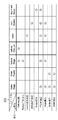
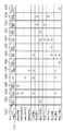
次に、工程結合装置506は、工程毎ユニット占有情報509を用いて、ロット間の時間損失を抑えるべく、上記2つの工程順序計画情報を結合させる。図8は、工程毎ユニット占有情報509の一例を示す図である。図8の表において、行は工程名801、列は構成部品名(ユニット名)802をそれぞれ示す。図8の表中に記される丸印は各工程を実施する際に占有されるユニットを意味する。一行目のレチクル交換(Reticle交換)工程においては、レチクルステージ(ReticleStage)123及びレチクルを搬送するレチクルチェンジャ(ReticleChanger)(不図示)のユニットを占有することを意味する。工程毎ユニット占有情報509を参照することによって、露光装置100の各工程で使用されるユニット情報を得ることができる。
Next, the process combining device 506 combines the two process order plan information using the
図9(b)は、図8の工程毎ユニット占有情報509を参照して、2つのロット工程順序計画情報を結合した例を示す図である。最初に、後方ロット(第2ロット)の開始工程を前方ロット(第1ロット)へ結合する方法を説明する。第1ロットの最終工程であるウエハ搬出工程912では、図8よりWaferStageとWafer Feederのユニットを占有することが分かる。第2ロットの開始工程にあたる913、914、915、916の各工程においても、図8から各工程で占有するユニット情報を得て、第1ロット最終工程912と第2ロット開始工程913、912と914、912と915、912と916の各々について占有するユニットが重複するか否かを判定する。この場合は、第1ロット最終工程912と第2ロット開始工程913、914、915、916の全てにユニットが重複することが無く、同時処理(第2ロットの先行処理開始)が可能である。次に、第1ロットの最終工程912から更に1つ前工程のウエハ露光工程911と第2ロット開始工程との間のユニット占有の重複有無を比較する。第1ロットのウエハ露光工程911は、第2ロットの913、915、916とユニットが重複するため、911の終了を待って開始する順序枝918、920、921で結合する。更に、1つ前工程のウエハアライメント工程910と第2ロットのスコープ調光工程914とを比較する。これらの工程間で重複するユニットが存在するため、第1ロットの工程910の終了を待って、第2ロットの工程914を開始する(919)。
FIG. 9B is a diagram showing an example in which two lot process order plan information is combined with reference to the
次に、前方ロット(第1ロット)の終了工程を後方ロット(第2ロット)へ結合する方法を説明する。上の結合方法と同様に、第1ロットの最終工程であるウエハN搬出工程912を、第2ロットの開始工程から順に占有ユニット情報を比較する。第2ロットの工程を順次進める中で、占有するユニットが重複したら結合する。図9(b)の場合、第1ロットのウエハN搬出工程912と第2ロットのTTLAF補正工程912との間で、WaferStageが重複しているので両者を結合する(922)。以上により、結合された工程順序計画情報を更新する。この工程順序計画情報での露光装置100の運転制御方法は、先に図5で説明した通りである。
Next, a method for combining the end process of the front lot (first lot) with the rear lot (second lot) will be described. In the same manner as the above combining method, the occupied unit information of the wafer
図4(b)は、本発明の好適な実施の形態において、ロットAとロットBを連続して実行した場合のタイムチャートである。ロットAの終了時間413より前にロットBが開始されている(414)ことが分かる。このオーバーラップは、図9に示した後方ロットの914、913、915、916が先行処理されたことによる。これによって、ロットを切換える際に発生する生産準備工程が先行処理され、製品ロット生産に要する時間が短縮されることがわかる。
FIG. 4B is a time chart when lot A and lot B are continuously executed in the preferred embodiment of the present invention. It can be seen that the lot B is started before the
[実施形態2]
実施形態1では、ウエハアライメントとウエハ露光の工程を共有する1つのウエハステージ116を使って順次処理を実施するシングルステージ型露光装置100について例示した。本実施形態2では、ウエハアライメントやウエハフォーカス面計測等のウエハ計測工程を計測ステージで、ウエハ露光処理を露光ステージで、それぞれ独立したステージを使って実施するツインステージ型露光装置1000について説明する。
[Embodiment 2]
In the first embodiment, the single-stage
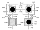
図10は、本発明の実施形態に係るツインステージ型露光装置1000の概略構成を示す図である。図10において、パルスレーザー光源1001、照明光学系1002、マスクステージ1004、投影レンズ1005及び露光ステージ1007は、図1のシングルステージ型露光装置100と同様の構成である。製品ロットの生産において、露光ステージ1007では、搬送されたウエハ1006に対しステップ・アンド・スキャン方式の露光工程が実施される。
FIG. 10 is a view showing a schematic configuration of a twin stage
計測ステージ1010は、3次元方向に移動可能であり、投影レンズ1005の光軸方向(Z方向)及びこの方向に直交する面内(X-Y面)を移動することができる。計測ステージに固定された移動鏡1011までの距離をレーザー干渉計1012で計測することによって、計測ステージ1010のX-Y面位置を検出することができる。レーザー干渉計1012によって計測ステージ1010の位置を検出し、モータ等の駆動手段(不図示)を制御することによって、計測ステージ1010を所定のX-Y面位置へ移動させる。
The
アライメントスコープ1013は、ウエハ1006に予め焼き付けてあるアライメントマーク(不図示)を観察するための顕微鏡である。アライメントスコープ1013を用いて、ウエハのアライメントマークを観察し、ウエハの下地回路パターンが正規位置からずれた量、例えばX、Y方向へのシフト量、チップ倍率誤差を計測する。
The
フォーカス面検出手段1014及び1015は、投光光学系1014からウエハ上のフォトレジストを感光させない非露光光から成る複数個の光束を投光し、ウエハ1006上に各々集光されて反射された光束を検出光学系1015に入射する。図示は省略したが、検出光学系1015内には、各反射光束に対応させて複数個の位置検出用の受光素子が配置されており、各位置検出用受光素子の受光面とウエハ上での各光束の反射点が結像光学系によって、略共役となるように構成されている。投影レンズ1005の光軸方向におけるウエハ面の位置ずれは、検出光学系1015内の位置検出用受光素子上の入射光束位置ずれとして計測される。
Focus
計測ステージ1010では、露光ステージ1007上のウエハ1006を露光する前に、アライメントスコープ1013及びフォーカス面検出手段1014、1015を使って、ウエハ下地回路パターンの各種ずれ量を計測する工程を実施し、後に露光ステージ1007上のウエハ1006を露光する時の補正量を得る。
In the
図11は、図10のツインステージを上から見た模式図であり、ロット処理する際のウエハ1006の流れを示している。感光剤が塗布されたウエハ1006がウエハフィーダー(不図示)によってウエハ搬入ステーション1103へ搬送されると(1106)、ウエハ1006を可動チャック1105へ吸着する。吸着されたウエハ1006は、可動チャック1105と一体となって、搬送装置としてのウエハ搬入ハンド1111によって計測ステージ1010へ搬入される(1107)。計測ステージ1010では、前述したようにウエハ1006の下地回路パターンの各種ずれ量が計測される。
FIG. 11 is a schematic view of the twin stage of FIG. 10 as viewed from above, and shows the flow of the
次に、計測したウエハ1006は、ウエハ移動ハンド1112によって可動チャック1105と一体となって露光ステージ1007へ移動される(1108)。露光ステージ1007では、予め計測ステージで計測されたウエハ下地回路パターンの各種ずれ量を補正しながら、ステップ・アンド・スキャン露光を繰り返す。露光が終了したウエハ1006は、ウエハ搬出ハンド1113によって可動チャック1105と一体となってウエハ搬出ステーションス1114へ搬出される(1109)。露光済みウエハ1006は、可動チャック1105との吸着が解除された後、ウエハフィーダー(不図示)によって搬送される(1110)。
Next, the measured
次に、ツインステージ型露光装置1000でのロット工程順序計画情報を図13(a)を用いて説明する。図13(a)は、単一ロットでウエハ2枚を露光処理する工程順序計画情報であり、図9(a)と同様に有向グラフで例示してある。ロット処理が開始されると、アライメントスコープ及びフォーカス面位置検出手段の計測光を調整するスコープ調光工程1301、1枚目のウエハを計測ステージへ搬入するMS搬入工程1302、照明条件設定工程1303、レーザー波長較正1304等のロット処理装置準備工程、レチクル交換工程1305等のマテリアル搬送工程の各5工程を同時に開始する。これは、各工程を実施する時に占有するユニットが重複しないからである。
Next, lot process order plan information in the twin stage
計測ステージ側では、1枚目のウエハが搬入され(1302)、且つ、スコープ調光1301されると、ウエハアライメント1306とウエハフォーカス計測工程1308を順次実行する。一方、露光ステージ側では、ウエハ搬送される露光準備を継続する。露光ステージの上部に構成されている投影レンズ1005の焦点面を検出するTTLAF補正1309は、1303、1304及びレチクルアライメント工程1307の終了を待って実行される。つまり、ロット処理開始してから計測ステージ側でウエハ準備、ウエハ計測準備、ウエハ計測処理を、露光ステージ側でレチクル準備、装置補正などの露光前準備工程を実行する。
On the measurement stage side, when the first wafer is loaded (1302) and scope dimming 1301 is performed, the
次に、ウエハ移動1310で工程1308まで終了した計測済みウエハを、工程1309まで露光前準備工程が終了した露光ステージへ移動する。ウエハ移動1310が終了すると、計測ステージ側では2枚目ウエハを搬入し(1311)、アライメント1312とフォーカス計測1313を1枚目のウエハと同様に順次実行し、計測済みウエハは露光ステージへ移動できるのを待つ。一方、ウエハが搬入された露光ステージ側では、ウエハのチップ領域をステップ・アンド・スキャン方式で露光する(1314)。この際、先に計測ステージで計測したウエハ下地回路パターンの各種ズレ量を補正しながら露光する。露光終了した後に、露光済みウエハは交換ステージへ搬出される(1315)。以後同様に、2枚目の計測済みウエハを露光ステージへ移動し(1316)、露光処理する。
Next, the wafer that has been measured up to step 1308 in
次に、図5に示した工程結合装置506は、ツインステージ型露光装置1000の工程毎ユニット占有情報509を用いて、ロット間の時間損失を抑えるべく2つの工程順序計画情報を結合させる。図12にツインステージ型露光装置1000の工程毎ユニット占有情報509の一例を示す。図12の表の行1201は工程名、列1203は構成部品名(ユニット名)をぞれぞれ示す。図12の表に記載のユニット名を図10、図11の装置構成図と比較すると、WaferInStation 1203はウエハ搬入ステーション1103、Reticle Stage 1204はマスクステージ1004、Reticle Changer1205はレチクル搬送ユニット(不図示)、Laser1206はパルスレーザー光源1001、Illumi. System1207は照明光学系1002、WaferOutHand 1208はウエハ搬出ハンド1113、ExpoStage 1209は露光ステージ1007、Wafer XferHand 1210はウエハ移動ハンド1112、MetroStage 1211は計測ステージ1010、WaferInHand 1212はウエハ搬入ハンド1111、Alignment Scope 1213はアライメントスコープ1013、Focusdetector 1214はフォーカス面検出手段1014、1015、WaferOut Station 1215はウエハ搬出ステーション1114にそれぞれ対応する。表中に記された丸印は、該工程を実施する際に占有されるユニットを意味し、工程毎ユニット占有情報509を参照することによって、露光装置1000の各工程で使用されるユニット情報を得ることができる。
Next, the process combining apparatus 506 shown in FIG. 5 combines two process order plan information using the
図13(b)は、図12の工程毎ユニット占有情報509を参照し、2つのロット工程順序計画情報を結合した例である。最初に、後方ロット(第2ロット)の開始工程を前方ロット(第1ロット)へ結合する方法を説明する。第1ロットの最終工程である最終ウエハES搬出工程1320では、図12よりWaferOut Station、Wafer OutHand及び、Expo Stageを占有する。同様に、第2ロットの開始工程にあたるスコープ調光1333、ウエハ1MS搬入1330、照明条件設定1325、レーザー波長較正1326、レチクル交換1327に対するユニット占有情報を得て、第1ロット最終工程と第2ロットの各開始工程を比較し、占有するユニットが重複するか否かを判定する。この場合は、重複するユニットが無く、先行処理が可能であると判断される。以後同様に、第1ロット最終工程から順次に前に戻りながら、第2ロット開始工程のユニット占有情報とを比較する。スコープ調光1333は第1ロット最終ウエハフォーカス計測1323の後に結合し(1340)、ウエハ1MS搬入1330は第1ロットの最終ウエハ移動1322の後に結合し(1339)、照明条件設定1325、レーザー波長較正1326及びレチクル交換1327は第1ロットの最終ウエハ露光1321の後にそれぞれ結合する(1336、1337及び1338)。
FIG. 13B is an example in which two lot process order plan information is combined with reference to the
次に、前方ロット(第1ロット)の最終工程を後方ロット(第2ロット)へ結合する。上の結合方法と同様に、第1ロットの最終工程である最終ウエハのES搬出工程1320と、第2ロット開始工程から順に占有ユニット情報を比較する。第2ロットの工程を順次進める中で、第2ロットのTTLAF補正工程1324との間で、ExpoStageが重複したので、その前に結合する(1335)。以上の計画は工程計画装置505が行う。図13(b)に示す工程順序計画情報に基づいて、露光装置1000を運転制御することによって、第1ロットで最終ウエハ計測1323及びウエハ移動1322が終了すると直ちに、第2ロットのスコープ調整1323とウエハ搬入1330とが開始されるため、ロット切換え時の時間損失を大幅に削減することができる。
Next, the final process of the front lot (first lot) is combined with the rear lot (second lot). Similar to the above combining method, the occupation unit information is compared sequentially from the final wafer
以上説明したように、本発明によれば、複数の製品ロットを連続して処理する場合に、トータルの処理時間が短縮でき、半導体デバイス等を効率的に生産することができる。特に、多品種小ロットの生産において大きな効果が期待できる。また、ツイン型のウエハステージを備えた露光装置において、本発明の効果が顕著にあらわれる。 As described above, according to the present invention, when a plurality of product lots are continuously processed, the total processing time can be shortened, and semiconductor devices and the like can be produced efficiently. In particular, a great effect can be expected in the production of a large variety of small lots. Further, in the exposure apparatus provided with a twin type wafer stage, the effect of the present invention is remarkably exhibited.
[応用例]
次に、上述の露光装置100、1000を利用した半導体デバイスの製造プロセスを説明する。図14は半導体デバイスの全体的な製造プロセスのフローを示す図である。ステップ1(回路設計)では半導体デバイスの回路設計を行う。ステップ2(マスク作製)では設計した回路パターンに基づいてマスクを作製する。
[Application example]
Next, a semiconductor device manufacturing process using the
一方、ステップ3(ウエハ製造)ではシリコン等の材料を用いてウエハを製造する。ステップ4(ウエハプロセス)は前工程と呼ばれ、上記のマスクとウエハを用いて、上記の露光装置によりリソグラフィ技術を利用してウエハ上に実際の回路を形成する。次のステップ5(組み立て)は後工程と呼ばれ、ステップ5によって作製されたウエハを用いて半導体チップ化する工程であり、アッセンブリ工程(ダイシング、ボンディング)、パッケージング工程(チップ封入)等の組み立て工程を含む。ステップ6(検査)ではステップ5で作製された半導体デバイスの動作確認テスト、耐久性テスト等の検査を行う。こうした工程を経て半導体デバイスが完成し、ステップ7でこれを出荷する。
On the other hand, in step 3 (wafer manufacture), a wafer is manufactured using a material such as silicon. Step 4 (wafer process) is called a pre-process, and an actual circuit is formed on the wafer by using the above-described exposure apparatus and lithography technology using the above-described mask and wafer. The next step 5 (assembly) is called a post-process, and is a process for forming a semiconductor chip using the wafer produced in
上記ステップ4のウエハプロセスは以下のステップを有する。ウエハの表面を酸化させる酸化ステップ、ウエハ表面に絶縁膜を成膜するCVDステップ、ウエハ上に電極を蒸着によって形成する電極形成ステップ、ウエハにイオンを打ち込むイオン打ち込みステップ、ウエハに感光剤を塗布するレジスト処理ステップ、上記の露光装置によって回路パターンをレジスト処理ステップ後のウエハに転写する露光ステップ、露光ステップで露光したウエハを現像する現像ステップ、現像ステップで現像したレジスト像以外の部分を削り取るエッチングステップ、エッチングが済んで不要となったレジストを取り除くレジスト剥離ステップ。これらのステップを繰り返し行うことによって、ウエハ上に多重に回路パターンを形成する。
The wafer process in
なお、露光装置は、上述したものに限られず、半導体集積回路等の半導体デバイスや、マイクロマシン、薄膜磁気ヘッド等の微細なパターンが形成されたデバイスの製造に利用され、原版であるマスクあるいはレチクルを介して基板としての半導体ウエハW上に光源からの露光エネルギーとしての露光光(この用語は、可視光、紫外光、EUV光、X線、電子線、荷電粒子線等の総称である)を投影系としての投影レンズ(この用語は、屈折レンズ、反射レンズ、反射屈折レンズシステム、荷電粒子レンズ等の総称である)を介して照射することによって、基板上に所望のパターンを形成するものであればよい。また、マスクを使用せずに半導体ウエハ上に回路パターンを直接描画してレジストを露光するタイプの露光装置であってもよい。 The exposure apparatus is not limited to the above-described one, but is used for manufacturing a semiconductor device such as a semiconductor integrated circuit or a device in which a fine pattern such as a micromachine or a thin film magnetic head is formed, and an original mask or reticle is used. Projecting exposure light as exposure energy from a light source onto a semiconductor wafer W as a substrate (this term is a generic term for visible light, ultraviolet light, EUV light, X-rays, electron beams, charged particle beams, etc.) What is necessary is to form a desired pattern on a substrate by irradiating through a projection lens as a system (this term is a general term for refractive lenses, reflective lenses, catadioptric lens systems, charged particle lenses, etc.) That's fine. Further, an exposure apparatus of a type that directly draws a circuit pattern on a semiconductor wafer without using a mask and exposes a resist may be used.
100…露光装置
102…レーザ制御装置
103…主制御装置
108…照明系制御装置
114…投影レンズ系制御装置
115…ウエハ(基板)
120…ウエハステージ制御装置
126…マスクステージ制御装置
508…ユニット制御装置
100 ... Exposure equipment
102 ... Laser control device
103 ... Main controller
108 ... Lighting system controller
114 ... Projection lens system controller
115 ... wafer (substrate)
120 ... Wafer stage controller
126… Mask stage controller
508 ... Unit controller
Claims (15)
各ロットに関して処理工程を計画する計画手段と、
前記計画手段により計画された、連続して処理されるべき第1及び第2のロットに関する処理工程を結合する結合手段と、
前記結合手段により結合された処理工程に基づいて、前記複数のユニットを制御する制御手段と
を有し、
前記結合手段は、前記第1ロットの処理の完了前且つ前記第2ロットの搬入前に、前記第1ロットに関し使用されなくなったユニットが前記第2ロットに関する第1の処理を開始するように、前記処理工程を結合することを特徴とする露光装置。 An exposure apparatus having a plurality of units,
A planning means for planning the process for each lot;
Combining means for combining processing steps relating to the first and second lots to be processed in succession planned by the planning means;
Control means for controlling the plurality of units based on the processing steps combined by the combining means;
The combining means is configured so that a unit that is no longer used for the first lot before the completion of the processing of the first lot and before the delivery of the second lot starts the first processing for the second lot. An exposure apparatus that combines the processing steps.
各ロットに関して処理工程を計画する計画段階と、
前記計画段階において計画された、連続して処理されるべき第1及び第2のロットに関する処理工程を結合する結合段階と、
前記結合段階において結合された処理工程に基づいて、前記複数のユニットを制御する制御段階と
を含み、
前記結合段階において、前記露光装置による前記第1ロットの処理の完了前且つ前記露光装置への前記第2ロットの搬入前に、前記第1ロットに関し使用されなくなったユニットが前記第2ロットに関する第1の処理を開始するように、前記処理工程を結合することを特徴とするデバイス製造方法。 A device manufacturing method for manufacturing a device using an exposure apparatus having a plurality of units,
A planning stage for planning the process for each lot;
A combining stage that combines the processing steps for the first and second lots to be processed in succession planned in the planning stage;
A control step for controlling the plurality of units based on the processing steps combined in the combining step, and
In the combining step, a unit that is no longer used for the first lot before the completion of the processing of the first lot by the exposure apparatus and before the second lot is carried into the exposure apparatus. A device manufacturing method, wherein the processing steps are combined so as to start the processing 1.
Priority Applications (2)
| Application Number | Priority Date | Filing Date | Title |
|---|---|---|---|
| JP2004106358A JP2005294473A (en) | 2004-03-31 | 2004-03-31 | Exposure apparatus, device manufacturing method, and device |
| US11/091,595 US7127311B2 (en) | 2004-03-31 | 2005-03-29 | Exposure apparatus and device manufacturing method |
Applications Claiming Priority (1)
| Application Number | Priority Date | Filing Date | Title |
|---|---|---|---|
| JP2004106358A JP2005294473A (en) | 2004-03-31 | 2004-03-31 | Exposure apparatus, device manufacturing method, and device |
Publications (1)
| Publication Number | Publication Date |
|---|---|
| JP2005294473A true JP2005294473A (en) | 2005-10-20 |
Family
ID=35055424
Family Applications (1)
| Application Number | Title | Priority Date | Filing Date |
|---|---|---|---|
| JP2004106358A Withdrawn JP2005294473A (en) | 2004-03-31 | 2004-03-31 | Exposure apparatus, device manufacturing method, and device |
Country Status (2)
| Country | Link |
|---|---|
| US (1) | US7127311B2 (en) |
| JP (1) | JP2005294473A (en) |
Cited By (6)
| Publication number | Priority date | Publication date | Assignee | Title |
|---|---|---|---|---|
| JP2007180180A (en) * | 2005-12-27 | 2007-07-12 | Dainippon Screen Mfg Co Ltd | Substrate processing equipment |
| JP2009071194A (en) * | 2007-09-14 | 2009-04-02 | Canon Inc | Semiconductor manufacturing apparatus, semiconductor manufacturing method, and device manufacturing method |
| JP2011022309A (en) * | 2009-07-15 | 2011-02-03 | Nsk Ltd | Method of controlling exposure apparatus |
| JP2012084793A (en) * | 2010-10-14 | 2012-04-26 | Nikon Corp | Exposure method, server device, exposure device and manufacturing method of device |
| JP2013213973A (en) * | 2012-04-03 | 2013-10-17 | Internatl Business Mach Corp <Ibm> | Mask design method, program, and mask design system |
| JP2015090872A (en) * | 2013-11-05 | 2015-05-11 | キヤノン株式会社 | Exposure apparatus, exposure method, and device manufacturing method |
Families Citing this family (4)
| Publication number | Priority date | Publication date | Assignee | Title |
|---|---|---|---|---|
| US7672747B2 (en) * | 2000-03-30 | 2010-03-02 | Lam Research Corporation | Recipe-and-component control module and methods thereof |
| JP2006108474A (en) * | 2004-10-07 | 2006-04-20 | Canon Inc | Exposure apparatus and device manufacturing method using the same |
| KR100856579B1 (en) * | 2007-01-18 | 2008-09-04 | 홍운식 | Method of managing exposure mask using exposure energy information of wafer accumulated by system that accumulates exposure energy information of wafer |
| JP5361239B2 (en) * | 2008-04-09 | 2013-12-04 | キヤノン株式会社 | Exposure apparatus and device manufacturing method |
Family Cites Families (14)
| Publication number | Priority date | Publication date | Assignee | Title |
|---|---|---|---|---|
| US5559710A (en) * | 1993-02-05 | 1996-09-24 | Siemens Corporate Research, Inc. | Apparatus for control and evaluation of pending jobs in a factory |
| US5444632A (en) * | 1994-04-28 | 1995-08-22 | Texas Instruments Incorporated | Apparatus and method for controlling and scheduling processing machines |
| US6584369B2 (en) * | 2000-02-02 | 2003-06-24 | Texas Instruments Incorporated | Method and system for dispatching semiconductor lots to manufacturing equipment for fabrication |
| JP2001228912A (en) * | 2000-02-18 | 2001-08-24 | Mitsubishi Electric Corp | Processing sequence control method and apparatus |
| EP1323059A2 (en) * | 2000-04-05 | 2003-07-02 | Pavilion Technologies, Inc. | System and method for enterprise modelling, optimization and control |
| JP4738563B2 (en) | 2000-04-21 | 2011-08-03 | キヤノン株式会社 | Semiconductor manufacturing apparatus and device manufacturing method |
| US6856848B2 (en) * | 2000-04-24 | 2005-02-15 | Matsushita Electric Industrial Co., Ltd. | Method and apparatus for controlling progress of product processing |
| CN1319115C (en) * | 2001-10-01 | 2007-05-30 | 株式会社半导体能源研究所 | System and method for producing combined products |
| US20030225474A1 (en) * | 2002-05-31 | 2003-12-04 | Gustavo Mata | Specialization of active software agents in an automated manufacturing environment |
| US6983189B2 (en) * | 2002-06-14 | 2006-01-03 | The Boeing Company | Systems and methods for manufacturing a product in a pull and push manufacturing system and associated methods and computer program products for modeling the same |
| US7778721B2 (en) * | 2003-01-27 | 2010-08-17 | Applied Materials, Inc. | Small lot size lithography bays |
| JP3833209B2 (en) * | 2003-10-24 | 2006-10-11 | キヤノン株式会社 | Exposure apparatus and device manufacturing method |
| US7257454B2 (en) * | 2003-11-21 | 2007-08-14 | Taiwan Semiconductor Manufacturing Company, Ltd. | Dynamically adjusting the distribution for dispatching lot between current and downstream tool by using expertise weighting mechanism |
| JP2006108474A (en) * | 2004-10-07 | 2006-04-20 | Canon Inc | Exposure apparatus and device manufacturing method using the same |
-
2004
- 2004-03-31 JP JP2004106358A patent/JP2005294473A/en not_active Withdrawn
-
2005
- 2005-03-29 US US11/091,595 patent/US7127311B2/en not_active Expired - Lifetime
Cited By (6)
| Publication number | Priority date | Publication date | Assignee | Title |
|---|---|---|---|---|
| JP2007180180A (en) * | 2005-12-27 | 2007-07-12 | Dainippon Screen Mfg Co Ltd | Substrate processing equipment |
| JP2009071194A (en) * | 2007-09-14 | 2009-04-02 | Canon Inc | Semiconductor manufacturing apparatus, semiconductor manufacturing method, and device manufacturing method |
| JP2011022309A (en) * | 2009-07-15 | 2011-02-03 | Nsk Ltd | Method of controlling exposure apparatus |
| JP2012084793A (en) * | 2010-10-14 | 2012-04-26 | Nikon Corp | Exposure method, server device, exposure device and manufacturing method of device |
| JP2013213973A (en) * | 2012-04-03 | 2013-10-17 | Internatl Business Mach Corp <Ibm> | Mask design method, program, and mask design system |
| JP2015090872A (en) * | 2013-11-05 | 2015-05-11 | キヤノン株式会社 | Exposure apparatus, exposure method, and device manufacturing method |
Also Published As
| Publication number | Publication date |
|---|---|
| US7127311B2 (en) | 2006-10-24 |
| US20050222699A1 (en) | 2005-10-06 |
Similar Documents
| Publication | Publication Date | Title |
|---|---|---|
| GB2155648A (en) | Exposing wafers | |
| JP4392879B2 (en) | Projection exposure apparatus and device manufacturing method | |
| JP3937580B2 (en) | Projection exposure apparatus and device manufacturing method using the same | |
| US7483764B2 (en) | Exposure apparatus and device manufacturing method | |
| JP2005310453A (en) | Light source device and exposure apparatus having the light source device | |
| WO2005036620A1 (en) | Exposure method, exposure device, and device manufacturing method | |
| JP2005294473A (en) | Exposure apparatus, device manufacturing method, and device | |
| JP2006032578A (en) | Light source device and exposure apparatus having the light source device | |
| JP2003068622A (en) | Exposure apparatus, control method therefor, and device manufacturing method | |
| JP2005012169A (en) | Exposure apparatus and device manufacturing method | |
| US6809798B1 (en) | Stage control method, exposure method, exposure apparatus and device manufacturing method | |
| US7257453B2 (en) | Exposure method and apparatus | |
| JP3618944B2 (en) | Illumination optical system and exposure apparatus using the same | |
| JP2001196293A (en) | Exposure apparatus and device manufacturing method using the same | |
| JP2001135559A (en) | Position measurement method and exposure method | |
| JP3554243B2 (en) | Projection exposure apparatus and device manufacturing method | |
| JP2004311639A (en) | Exposure apparatus, exposure method, and device manufacturing method | |
| JPH09223662A (en) | Illumination apparatus, scanning exposure apparatus, and device manufacturing method using the same | |
| JP5653182B2 (en) | Exposure method, exposure apparatus, and device manufacturing method | |
| JP2004319780A (en) | Exposure method, exposure apparatus, and device manufacturing method | |
| JP2011146449A (en) | Flare measuring method, exposure method and apparatus, and method for manufacturing device | |
| KR20010078323A (en) | Method and apparatus for exposure, and method of manufacturing device | |
| JP2009290243A (en) | Projection exposure device and method of manufacturing device | |
| JP2025006430A (en) | Management device, management method, and program | |
| CN119365826A (en) | System for path compensation with moving objective lens |
Legal Events
| Date | Code | Title | Description |
|---|---|---|---|
| A977 | Report on retrieval |
Free format text: JAPANESE INTERMEDIATE CODE: A971007 Effective date: 20060407 |
|
| A131 | Notification of reasons for refusal |
Free format text: JAPANESE INTERMEDIATE CODE: A131 Effective date: 20070122 |
|
| A761 | Written withdrawal of application |
Free format text: JAPANESE INTERMEDIATE CODE: A761 Effective date: 20070320 |