JP2005294449A - Semiconductor device inspection method and inspection apparatus - Google Patents
Semiconductor device inspection method and inspection apparatus Download PDFInfo
- Publication number
- JP2005294449A JP2005294449A JP2004105913A JP2004105913A JP2005294449A JP 2005294449 A JP2005294449 A JP 2005294449A JP 2004105913 A JP2004105913 A JP 2004105913A JP 2004105913 A JP2004105913 A JP 2004105913A JP 2005294449 A JP2005294449 A JP 2005294449A
- Authority
- JP
- Japan
- Prior art keywords
- current
- semiconductor device
- value
- measurement
- laser chip
- Prior art date
- Legal status (The legal status is an assumption and is not a legal conclusion. Google has not performed a legal analysis and makes no representation as to the accuracy of the status listed.)
- Pending
Links
Images


Landscapes
- Testing Of Individual Semiconductor Devices (AREA)
- Semiconductor Lasers (AREA)
Abstract
【課題】 高信頼性を確保しつつ、かつ、短時間で半導体レーザチップなどの半導体装置を検査する方法および検査装置を提供することが課題である。
【解決手段】 半導体装置に複数の電流値の電流を印加したときの半導体装置の状態を表す特性値を測定する半導体装置の検査方法であって、設定される電流値の電流を印加して、半導体装置の状態を表す特性値を測定する測定工程と、測定工程で測定された特性値に基づいて、次に半導体装置に印加する電流の電流値を演算して更新設定する設定工程と、測定工程および設定工程を、予め定める条件を満たすまで、繰返す繰返し工程とを含む半導体装置の検査方法による。
【選択図】 図1
To provide a method and an inspection apparatus for inspecting a semiconductor device such as a semiconductor laser chip in a short time while ensuring high reliability.
A semiconductor device inspection method for measuring a characteristic value representing a state of a semiconductor device when a plurality of current values are applied to the semiconductor device, wherein a current having a set current value is applied, A measurement process for measuring a characteristic value representing the state of the semiconductor device, a setting process for calculating and updating the current value of the current to be applied to the semiconductor device based on the characteristic value measured in the measurement process, and a measurement According to the semiconductor device inspection method, the process and the setting process are repeated until a predetermined condition is satisfied.
[Selection] Figure 1
Description
本発明は、半導体レーザチップなどの半導体装置を検査する方法および検査装置に関する。 The present invention relates to a method and an inspection apparatus for inspecting a semiconductor device such as a semiconductor laser chip.
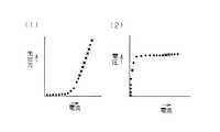
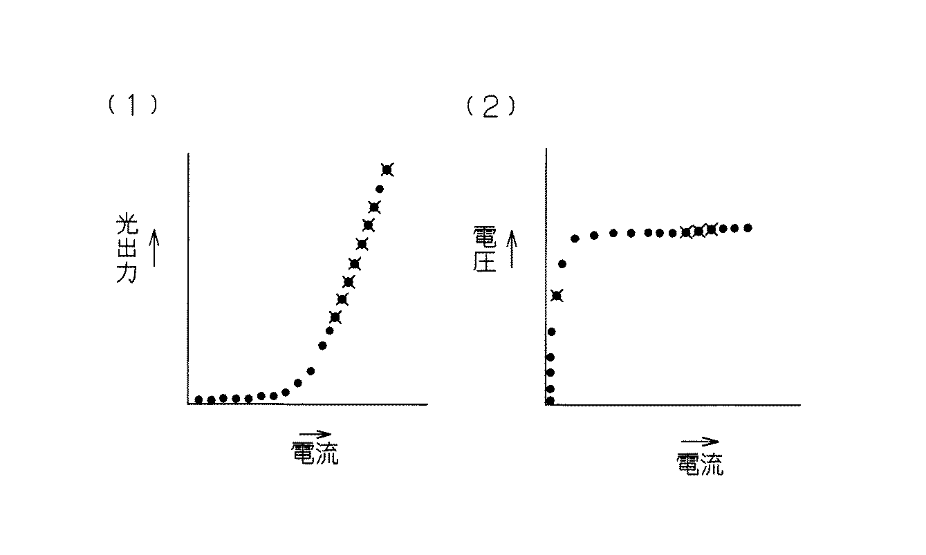
図9は、従来の半導体レーザチップの測定方法を示すグラフである。図9(1)は、パルス電流に対する光出力を示すグラフである。図9(2)は、パルス電流に対する電圧を示すグラフである。パルス電流の電流値を一定の間隔をとって徐々に増大させながら、電流値、レーザチップの光出力およびレーザチップ端子間の電圧を測定する。この場合、印加したときの全体のカーブを目視で確認することができる。しかし、必要な性能を測定するためには、ステップ幅をかなり小さく採らなければならないので測定するのに多大な時間を要していた。 FIG. 9 is a graph showing a conventional method for measuring a semiconductor laser chip. FIG. 9A is a graph showing the optical output with respect to the pulse current. FIG. 9 (2) is a graph showing the voltage with respect to the pulse current. While gradually increasing the current value of the pulse current at regular intervals, the current value, the optical output of the laser chip, and the voltage between the laser chip terminals are measured. In this case, the entire curve when applied can be visually confirmed. However, in order to measure the required performance, it is necessary to take a very small step width. Therefore, it takes a lot of time for the measurement.
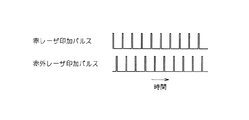
図10は、従来の半導体レーザチップのパルス発生タイミングを示すタイムチャートである。これは、2つの発光点を有する半導体レーザチップの各発光点の電流−光出力および電流−電圧を測定する方法を示す。たとえば、一方が赤色のレーザを発光し、他方が赤外線のレーザを発光する半導体レーザチップの場合、電流値を一定間隔で増大させながらパルス電流を印加して赤色のレーザを発光させて、赤色レーザの電流−光出力の測定を終え、その後赤色レーザの場合と同様に赤外線レーザの電流-光出力および電流−電圧の測定を行う。 FIG. 10 is a time chart showing pulse generation timing of a conventional semiconductor laser chip. This shows a method of measuring the current-light output and current-voltage of each light emitting point of a semiconductor laser chip having two light emitting points. For example, in the case of a semiconductor laser chip in which one emits a red laser and the other emits an infrared laser, a red laser is emitted by applying a pulse current while increasing the current value at regular intervals. After the measurement of the current-light output is completed, the current-light output and current-voltage of the infrared laser are measured in the same manner as in the case of the red laser.
測定するのに多大な時間を要するという問題を解決する典型的な技術は、特許文献1に記載されている。特許文献1の半導体レーザ素子の測定装置は、半導体レーザ素子の電流−光出力特性及び、電流−電圧特性を測定し、半導体レーザ素子の発振特性を測定するように構成され、かつ半導体レーザ素子に印加する電流に、ステップ・パルス・バイアス電流を用いることを特徴としている。
A typical technique for solving the problem that it takes a long time to measure is described in
他の技術が、特許文献2に記載されている。特許文献2のタイミング差測定装置は、E−O計測装置,波形記憶演算装置で構成されている。E−O計測装置は、被測定デバイスの電気信号をストローブ光にてサンプリングして信号波形を測定するもので、非常に高い時間分解能を有している点に特徴がある。
Another technique is described in
さらに、他の技術は、特許文献3に記載されている。特許文献3の半導体製造装置は、半導体装置の画像認識を行う画像認識手段と、前記半導体装置を画像データ取り込みのために照明する照明機構とを具備する半導体製造装置において、前記照明機構に前記半導体装置の実照明量を検出して、自動的に照明量を所定の状態に制御する制御手段を備えたことを特徴とする。 Further, another technique is described in Patent Document 3. The semiconductor manufacturing apparatus disclosed in Patent Document 3 is a semiconductor manufacturing apparatus including an image recognition unit that performs image recognition of a semiconductor device and an illumination mechanism that illuminates the semiconductor device for capturing image data. It is characterized by comprising a control means for detecting the actual illumination amount of the apparatus and automatically controlling the illumination amount to a predetermined state.
そして、他の技術は、特許文献4に記載されている。特許文献4の半導体製造装置の認識装置は、被処理物を照射するランプ、上記被処理物を撮像するテレビカメラ、このテレビカメラの映像を画像処理する画像処理手段、この画像処理手段が認識不能と判断したときに信号を出力する制御手段、この制御手段の出力信号に基づき、予め設定されていた上記ランプの光量を増加させるランプ光量増加手段を備えるものである。 Another technique is described in Patent Document 4. A recognition apparatus for a semiconductor manufacturing apparatus disclosed in Patent Document 4 includes a lamp that irradiates an object to be processed, a television camera that captures the object to be processed, an image processing unit that performs image processing on video from the television camera, and the image processing unit cannot recognize Control means for outputting a signal when it is determined, and lamp light quantity increasing means for increasing the light quantity of the lamp set in advance based on the output signal of the control means.
特許文献3および特許文献4の技術によれば、半導体チップを一定光量で照明することができる。 According to the techniques of Patent Document 3 and Patent Document 4, the semiconductor chip can be illuminated with a constant light amount.
従来の検査方法では、半導体レーザチップの性能を評価するため非常に多くの回数のパルス電流を印加しなければならない。そのため測定に要する印加時間が長くなるので半導体レーザチップに与えるダメージが大きくなることが問題であった。また、測定時間が長くなることで多大な時間を要していた。 In the conventional inspection method, a very large number of pulse currents must be applied in order to evaluate the performance of the semiconductor laser chip. For this reason, the application time required for the measurement becomes long, so that the damage given to the semiconductor laser chip becomes a problem. In addition, a long time is required due to the long measurement time.
特許文献1の技術では、電流−微分効率特性(I−dL/dI :Iは電流値、Lは光出力を表す)、電流−微分抵抗特性(I−dV/dI :Iは電流値、Vは電圧を表す)を効率よく測定することはできても、他の特性の測定に対しては有用ではない。
In the technique of
本発明の目的は、半導体レーザチップなどの半導体装置の検査によるダメージが少なく、短時間でかつ精度よく半導体レーザチップなどの半導体装置を検査する方法および検査装置を提供することにある。 An object of the present invention is to provide a method and an inspection apparatus for inspecting a semiconductor device such as a semiconductor laser chip in a short time and with high accuracy, with little damage caused by inspection of a semiconductor device such as a semiconductor laser chip.
本発明は、半導体装置に複数の電流値の電流を印加したときの半導体装置の状態を表す特性値を測定する半導体装置の検査方法であって、
設定される電流値の電流を半導体装置に印加して、半導体装置の状態を表す特性値を測定する測定工程と、
測定工程で測定された特性値に基づいて、次に半導体装置に印加する電流の電流値を演算して更新設定する設定工程と、
測定工程および設定工程を、予め定める条件を満たすまで、繰返す繰返し工程とを含むことを特徴とする半導体装置の検査方法である。
The present invention is a semiconductor device inspection method for measuring a characteristic value representing a state of a semiconductor device when a current having a plurality of current values is applied to the semiconductor device,
A measuring step of applying a current of a set current value to the semiconductor device and measuring a characteristic value representing a state of the semiconductor device;
Based on the characteristic value measured in the measurement step, a setting step for calculating and updating the current value of the current to be applied to the semiconductor device next,
A method for inspecting a semiconductor device, comprising: repeating a measurement process and a setting process until a predetermined condition is satisfied.
本発明に従えば、設定工程によって測定項目に応じて測定に必要な次の電流値を演算して更新設定することができる。測定項目上、測定する必要のある電流値を、測定工程により得られた値を基に設定工程で設定できる。設定された電流値の電流を印加して半導体装置の特性値を測定することによって精度よく測定することができ、また、不要な測定をする必要がないので、短時間で半導体装置を検査することができる。したがって、半導体装置に対するダメージを低減することができるため高信頼性を確保することができる。 According to the present invention, the next current value required for the measurement can be calculated and updated by the setting process according to the measurement item. On the measurement item, the current value that needs to be measured can be set in the setting step based on the value obtained in the measurement step. It is possible to measure the characteristic value of the semiconductor device accurately by applying the current of the set current value, and it is not necessary to perform unnecessary measurement, so the semiconductor device is inspected in a short time Can do. Therefore, since damage to the semiconductor device can be reduced, high reliability can be ensured.
また本発明は、複数の半導体装置の検査を並行して実行する半導体装置の検査方法であって、
前記測定工程では、各半導体装置に順次選択的に電流を印加することを特徴とする。
Further, the present invention is a semiconductor device inspection method for performing inspection of a plurality of semiconductor devices in parallel,
In the measurement step, a current is selectively applied to each semiconductor device sequentially.
本発明に従えば、複数の半導体装置の検査を並列して実行し、各半導体装置に順次選択的に電流を印加して測定するので、各半導体装置毎に検査を直列して実行するよりも短時間で複数の半導体装置の検査を全部終えることができる。また、順次選択的に電流を印加して測定するので各半導体装置毎に特性値測定装置を設ける必要がない。 According to the present invention, the inspection of a plurality of semiconductor devices is executed in parallel, and the current is selectively applied to each semiconductor device in order to measure. Therefore, the inspection is performed in series for each semiconductor device. All inspections of a plurality of semiconductor devices can be completed in a short time. Further, since the current is sequentially applied and measured, it is not necessary to provide a characteristic value measuring device for each semiconductor device.
また本発明は、前記測定工程では、同一周期で異なる位相のパルス電流を印加することを特徴とする。 In the measurement step, pulse currents having different phases are applied in the same cycle.
本発明に従えば、同一周期で異なる位相のパルス電流を各半導体装置に印加することによって、複雑な調停手段を用いて各半導体装置に電流を印加して測定する場合よりも簡易に、順次選択的にパルス電流を各半導体装置に印加して各半導体装置を測定することができる。 According to the present invention, by sequentially applying pulse currents of different phases in the same period to each semiconductor device, it is possible to select sequentially more easily than when applying current to each semiconductor device using a complicated arbitration means and measuring. In addition, each semiconductor device can be measured by applying a pulse current to each semiconductor device.
また本発明は、前記設定工程では、測定値の変化が急であると予測される第一測定領域および特性値の限界値の近傍である第二測定領域においては、電流の変化幅を他の領域に比べて小さい幅とすることを特徴とする。 According to the present invention, in the setting step, in the first measurement region where the change in the measurement value is predicted to be abrupt and the second measurement region in the vicinity of the limit value of the characteristic value, The width is smaller than that of the region.
本発明に従えば、測定値の変化が急であると予測される第一測定領域を測定するときおよび特性値の限界値近傍は、他の領域を測定するときと比べて印加電流の変化幅を小さい幅とするので、精度の高い測定をできる検査方法を提供することができる。 According to the present invention, when measuring the first measurement region where the change in the measured value is expected to be sudden, and in the vicinity of the limit value of the characteristic value, the change width of the applied current compared to when measuring the other region Since the width is small, it is possible to provide an inspection method capable of measuring with high accuracy.
また本発明は、前記半導体装置が半導体レーザチップであり、前記特性値が光出力値および電圧値であることを特徴とする。 According to the present invention, the semiconductor device is a semiconductor laser chip, and the characteristic values are an optical output value and a voltage value.
本発明に従えば、半導体装置が半導体レーザチップであり、特性値が光出力値および電圧値であるので、半導体レーザチップの検査を好適にすることができる検査方法を提供することができる。 According to the present invention, since the semiconductor device is a semiconductor laser chip and the characteristic values are an optical output value and a voltage value, it is possible to provide an inspection method that can favorably inspect the semiconductor laser chip.
また本発明は、パルス電流を印加して光出力値および電圧値を測定する半導体レーザチップの検査方法であって、
前記設定工程では、測定項目を評価するのに必要な測定領域以外の測定領域を測定する際、測定項目を評価する際のパルス電流の最大パルス電流値間の変化幅を超えて、かつ、前記半導体レーザチップのリミットパワーを前記半導体レーザチップの現時点でのパワーで減算してこの減算値を前記半導体レーザチップのMax微分効率で除算した値を超えないパルス電流の最大パルス電流値間の変化幅である電流値を設定することを特徴とする。
Further, the present invention is a semiconductor laser chip inspection method for measuring a light output value and a voltage value by applying a pulse current,
In the setting step, when measuring a measurement region other than the measurement region necessary for evaluating the measurement item, exceeding the change width between the maximum pulse current values of the pulse current when evaluating the measurement item, and the above The change width between the maximum pulse current values of the pulse current not exceeding the value obtained by subtracting the limit power of the semiconductor laser chip by the current power of the semiconductor laser chip and dividing this subtracted value by the Max differential efficiency of the semiconductor laser chip A current value is set.
本発明に従えば、測定項目を評価するために必要な測定領域でない場合には、測定項目を評価する際の変化幅よりも大きな変化幅で電流値を変化させるのでパルス電流の印加回数を低減することができる。パルス電流の印加回数の低減によって、短時間での検査を可能にし、半導体レーザチップの検査によるダメージの低減を可能にする。半導体レーザチップのリミットパワーを半導体レーザチップの現時点でのパワーで減算してこの減算値を半導体レーザチップのMax微分効率で除算した値を超えない変化幅で変化させた電流値のパルス電流を半導体レーザチップに印加しても、リミットパワーを超えないことが保証されているので、半導体レーザチップを破壊しない。 According to the present invention, when the measurement area is not necessary for evaluating the measurement item, the current value is changed with a change width larger than the change width when the measurement item is evaluated, so that the number of application times of the pulse current is reduced. can do. By reducing the number of times the pulse current is applied, inspection can be performed in a short time, and damage due to inspection of the semiconductor laser chip can be reduced. The pulse current of the current value obtained by subtracting the limit power of the semiconductor laser chip by the current power of the semiconductor laser chip and changing the subtracted value by the value obtained by dividing the subtraction value by the Max differential efficiency of the semiconductor laser chip is the semiconductor. Even if it is applied to the laser chip, it is guaranteed that the limit power will not be exceeded, so the semiconductor laser chip is not destroyed.
また本発明は、半導体装置に電流を印加するための電流印加手段と、
半導体装置の状態を表す特性値を測定する測定手段と、
測定手段で測定された特性値に基づいて、次に半導体装置に印加する電流の電流値を演算して更新設定する演算処理手段とを含むことを特徴とする半導体装置の検査装置である。
The present invention also includes a current applying means for applying a current to the semiconductor device,
Measuring means for measuring characteristic values representing the state of the semiconductor device;
An inspection apparatus for a semiconductor device, comprising: arithmetic processing means for calculating and updating a current value of a current to be applied to the semiconductor device next based on the characteristic value measured by the measuring means.
本発明に従えば、電流を印加された半導体装置の特性を測定する測定手段により特性値を得ることができる。この特性値に基づいて演算処理手段は次に印加すべき電流の電流値を演算して設定する。設定された電流値に基づいて電流印加手段は半導体装置に電流を印加する。そして、再び測定手段により特性値を得る。得られた特性値に基づいて電流値設定手段は次に印加すべき電流の電流値を演算して設定する。これらの測定工程および設定工程を繰返して予め定める終了条件に達した場合には、検査を終える。したがって、検査に必要な電流値の電流を流すことができるので精度が高い検査を行うことができ、検査に不要な測定を省くことができるので半導体装置に与えるダメージが少なく済み高信頼性を確保しつつ短時間で検査を終えることができる検査装置を提供することができる。 According to the present invention, the characteristic value can be obtained by the measuring means for measuring the characteristic of the semiconductor device to which a current is applied. Based on this characteristic value, the arithmetic processing means calculates and sets the current value of the current to be applied next. Based on the set current value, the current applying means applies a current to the semiconductor device. Then, the characteristic value is obtained again by the measuring means. Based on the obtained characteristic value, the current value setting means calculates and sets the current value of the current to be applied next. When these measurement steps and setting steps are repeated to reach a predetermined end condition, the inspection is finished. Therefore, since the current of the current value necessary for inspection can be passed, highly accurate inspection can be performed, and unnecessary measurement for inspection can be omitted, so that damage to the semiconductor device is reduced and high reliability is ensured. In addition, it is possible to provide an inspection apparatus capable of completing the inspection in a short time.
また本発明は、複数の半導体装置の検査を並行して実行する半導体装置の検査装置であって、
前記電流印加手段では、各半導体装置に順次選択的に電流を印加することを特徴とする。
Further, the present invention is a semiconductor device inspection apparatus that executes inspection of a plurality of semiconductor devices in parallel,
The current application means selectively applies a current to each semiconductor device sequentially.
本発明に従えば、複数の半導体装置の検査を並列して実行し、各半導体装置に順次選択的に電流を印加して測定するので、各半導体装置毎に検査を直列して実行するよりも短時間で複数の半導体装置の検査を全部終えることができる検査装置を提供できる。また、順次選択的に電流を印加して測定するので各半導体装置毎に特性値測定装置を設ける必要がなく経済的である。 According to the present invention, the inspection of a plurality of semiconductor devices is executed in parallel, and the current is selectively applied to each semiconductor device in order to measure. Therefore, the inspection is performed in series for each semiconductor device. It is possible to provide an inspection apparatus capable of completing all inspections of a plurality of semiconductor devices in a short time. Further, since current is selectively applied and measured sequentially, there is no need to provide a characteristic value measuring device for each semiconductor device, which is economical.
また本発明は、前記電流印加手段では、同一周期で異なる位相のパルス電流を印加することを特徴とする。 Further, the present invention is characterized in that the current applying means applies pulse currents of different phases at the same period.
本発明に従えば、同一周期で異なる位相のパルス電流を各半導体装置に印加することによって、複雑な調停手段を用いて各半導体装置に電流を印加して測定する場合よりも簡易に、順次選択的にパルス電流を各半導体装置に印加することができる検査装置を実現することができる。 According to the present invention, by sequentially applying pulse currents of different phases in the same period to each semiconductor device, it is possible to select sequentially more easily than when applying current to each semiconductor device using a complicated arbitration means and measuring. Thus, an inspection apparatus capable of applying a pulse current to each semiconductor device can be realized.
また本発明は、前記演算処理手段は、測定値の変化が急であると予測される第一測定領域および特性値の限界値の近傍である第二測定領域においては、電流の変化幅を他の領域に比べて小さい幅とすることを特徴とする。 In the present invention, the arithmetic processing unit may change the current change width in the first measurement region where the change in the measurement value is predicted to be sudden and the second measurement region in the vicinity of the limit value of the characteristic value. The width is smaller than that of the region.
本発明に従えば、測定値の変化が急であると予測される第一測定領域を測定するときおよび特性値の限界値近傍は、他の領域を測定するときと比べて印加電流の変化幅を小さい幅とするので、精度の高い測定をできる検査装置を提供することができる。 According to the present invention, when measuring the first measurement region where the change in the measured value is expected to be sudden, and in the vicinity of the limit value of the characteristic value, the change width of the applied current compared to when measuring the other region Since the width is small, it is possible to provide an inspection apparatus capable of measuring with high accuracy.
また本発明は、前記半導体装置が半導体レーザチップであり、前記特性値が光出力値および電圧値であることを特徴とする。 According to the present invention, the semiconductor device is a semiconductor laser chip, and the characteristic values are an optical output value and a voltage value.
本発明に従えば、半導体装置が半導体レーザチップであり、特性値が光出力値および電圧値であるので、半導体レーザチップの検査を好適にすることができる検査装置を提供することができる。 According to the present invention, since the semiconductor device is a semiconductor laser chip and the characteristic values are an optical output value and a voltage value, it is possible to provide an inspection apparatus that can make the inspection of the semiconductor laser chip suitable.
また本発明は、パルス電流を印加して光出力値および電圧値を測定する半導体レーザチップの検査装置であって、
前記演算処理手段は、測定項目を評価するのに必要な測定領域以外の測定領域を、測定項目を評価する際のパルス電流の最大パルス電流値間の変化幅を超えて、かつ、前記半導体レーザチップのリミットパワーを前記半導体レーザチップの現時点でのパワーで減算してこの減算値を前記半導体レーザチップのMax微分効率で除算した値を超えないパルス電流の最大パルス電流値間の変化幅である電流値を設定することを特徴とする。
Further, the present invention is a semiconductor laser chip inspection apparatus for measuring a light output value and a voltage value by applying a pulse current,
The arithmetic processing means has a measurement region other than the measurement region necessary for evaluating the measurement item, exceeding a change width between the maximum pulse current values of the pulse current when evaluating the measurement item, and the semiconductor laser. This is the change width between the maximum pulse current values of the pulse current that does not exceed the value obtained by subtracting the limit power of the chip by the current power of the semiconductor laser chip and dividing this subtracted value by the Max differential efficiency of the semiconductor laser chip. A current value is set.
本発明に従えば、測定項目を評価するために必要な測定領域でない場合には、測定項目を評価する際の変化幅よりも大きな変化幅で電流値を変化させるのでパルス電流の印加回数を低減することができる。パルス電流の印加回数の低減によって、短時間での検査を可能にし、半導体レーザチップの検査によるダメージの低減を可能にする。半導体レーザチップのリミットパワーを半導体レーザチップの現時点でのパワーで減算してこの減算値を半導体レーザチップのMax微分効率で除算した値を超えない変化幅で変化させた電流値のパルス電流を半導体レーザチップに印加しても、リミットパワーを超えないことが保証されているので、半導体レーザチップを破壊しない。 According to the present invention, when the measurement area is not necessary for evaluating the measurement item, the current value is changed with a change width larger than the change width when the measurement item is evaluated, so that the number of application times of the pulse current is reduced. can do. By reducing the number of times the pulse current is applied, inspection can be performed in a short time, and damage due to inspection of the semiconductor laser chip can be reduced. The pulse current of the current value obtained by subtracting the limit power of the semiconductor laser chip by the current power of the semiconductor laser chip and changing the subtracted value by the value obtained by dividing the subtraction value by the Max differential efficiency of the semiconductor laser chip is the semiconductor. Even if it is applied to the laser chip, it is guaranteed that the limit power will not be exceeded, so the semiconductor laser chip is not destroyed.
本発明によれば、測定に必要な電流値の電流を印加して半導体装置の特性値を測定することによって精度よく測定することができ、また、不要な測定をする必要がないので、短時間で半導体装置を検査することができる。したがって、半導体装置に対するダメージを低減することができるため高信頼性を確保することができる。 According to the present invention, it is possible to accurately measure by applying a current having a current value necessary for measurement and measuring the characteristic value of the semiconductor device, and it is not necessary to perform unnecessary measurement. The semiconductor device can be inspected. Therefore, since damage to the semiconductor device can be reduced, high reliability can be ensured.
本発明によれば、短時間で各半導体装置の検査を終えることができる。したがって、全体での検査時間を短縮することができる。また、各半導体装置毎に特性値測定装置を設ける必要がない。 According to the present invention, the inspection of each semiconductor device can be completed in a short time. Therefore, the overall inspection time can be shortened. Further, it is not necessary to provide a characteristic value measuring device for each semiconductor device.
本発明によれば、簡易に、順次選択的にパルス電流を各半導体装置に印加することができる。 According to the present invention, it is possible to easily and sequentially apply a pulse current to each semiconductor device.
本発明によれば、精度の高い検査結果を得ることができる検査方法を提供することができる。 According to the present invention, it is possible to provide an inspection method capable of obtaining a highly accurate inspection result.
本発明によれば、半導体レーザチップの検査を好適にすることができる検査方法を提供することができる。 ADVANTAGE OF THE INVENTION According to this invention, the test | inspection method which can make the test | inspection of a semiconductor laser chip suitable can be provided.
本発明によれば、パルス電流の印加回数を低減することができる。パルス電流の印加回数の低減によって、短時間での検査を可能にし、半導体レーザチップの検査によるダメージの低減を可能にする。さらに、リミットパワーを超えないことが保証されているので、半導体レーザチップを破壊しない。 According to the present invention, the number of application times of pulse current can be reduced. By reducing the number of times the pulse current is applied, inspection can be performed in a short time, and damage due to inspection of the semiconductor laser chip can be reduced. Furthermore, since it is guaranteed that the limit power is not exceeded, the semiconductor laser chip is not destroyed.
本発明によれば、検査に必要な電流値の電流を流すことができるので信頼性が高い検査を行うことができ、検査に不要な測定を省くことができるので短時間で検査を終えることができる検査装置を提供することができる。この検査装置では、短時間で検査を終えることができるので半導体装置に与えるダメージを低減することができる。 According to the present invention, since a current having a current value required for inspection can be passed, highly reliable inspection can be performed, and unnecessary measurement for inspection can be omitted, so that the inspection can be completed in a short time. An inspection device capable of being provided can be provided. In this inspection apparatus, since the inspection can be completed in a short time, damage to the semiconductor device can be reduced.
本発明によれば、短時間で各半導体装置の検査を終える検査装置を提供することができる。したがって、全体での検査時間を短縮することができる。また、各半導体装置毎に特性値測定装置を設ける必要がない。 ADVANTAGE OF THE INVENTION According to this invention, the inspection apparatus which finishes the test | inspection of each semiconductor device in a short time can be provided. Therefore, the overall inspection time can be shortened. Further, it is not necessary to provide a characteristic value measuring device for each semiconductor device.
本発明によれば、簡易に、順次選択的にパルス電流を各半導体装置に印加することができる検査装置を実現することができる。 According to the present invention, it is possible to realize an inspection apparatus capable of simply and sequentially applying a pulse current to each semiconductor device.
本発明によれば、精度の高い検査結果を得ることができる検査装置を提供することができる。 According to the present invention, it is possible to provide an inspection apparatus capable of obtaining a highly accurate inspection result.
本発明によれば、半導体レーザチップの検査を好適にすることができる検査装置を提供することができる。 ADVANTAGE OF THE INVENTION According to this invention, the test | inspection apparatus which can make the test | inspection of a semiconductor laser chip suitable can be provided.
本発明によれば、パルス電流の印加回数を低減することができる。パルス電流の印加回数の低減によって、短時間での検査を可能にし、半導体レーザチップの検査によるダメージの低減を可能にする。さらに、リミットパワーを超えないことが保証されているので、半導体レーザチップを破壊しない。 According to the present invention, the number of application times of pulse current can be reduced. By reducing the number of times the pulse current is applied, inspection can be performed in a short time, and damage due to inspection of the semiconductor laser chip can be reduced. Furthermore, since it is guaranteed that the limit power is not exceeded, the semiconductor laser chip is not destroyed.
図1は、本発明の第1実施形態を示す半導体装置の検査方法を示すフローチャートである。この実施形態は、半導体装置に複数の電流値の電流を印加したときに半導体装置の特性値を測定する半導体装置の検査方法であり、測定工程と、設定工程と、繰返し工程を含む半導体装置の検査方法である。 FIG. 1 is a flowchart showing a semiconductor device inspection method according to a first embodiment of the present invention. This embodiment is a semiconductor device inspection method for measuring characteristic values of a semiconductor device when a plurality of current values are applied to the semiconductor device, and includes a measurement process, a setting process, and a repetition process. Inspection method.
本発明で検査される半導体装置には、半導体レーザチップ11および発光ダイオードなどの半導体発光素子、トランジスタ、LSIなどの半導体素子などが含まれるものとし、パッケージに封じされた半導体レーザ装置、LSIなどでもよい。このうち、検査にパルス電流を用い、レーザ光を射出する半導体レーザチップ11を好適に検査することができる。半導体レーザチップ11を検査する場合、主として光出力、電流を印加する端子間の電圧などの特性値を測定する。その他出力される光の波長、半導体レーザチップ11の温度などの特性値を測定することもできる。 Semiconductor devices to be inspected in the present invention include semiconductor laser chips 11 and semiconductor light emitting elements such as light emitting diodes, semiconductor elements such as transistors and LSIs, and semiconductor laser devices and LSIs sealed in packages. Good. Among these, the semiconductor laser chip 11 that emits laser light can be suitably inspected using a pulse current for inspection. When inspecting the semiconductor laser chip 11, characteristic values such as light output and voltage between terminals to which current is applied are mainly measured. Other characteristic values such as the wavelength of the output light and the temperature of the semiconductor laser chip 11 can also be measured.
ステップS1で、最初に印加すべき電流値を設定して半導体レーザチップ11の検査が始まる。ステップS2で、半導体装置に設定値のパルス電流を印加して、設定値のパルス電流が印加された半導体レーザチップの光出力および電圧値などの特性値を測定する測定工程を実施する。ステップS3で、予め定められた終了条件を満たすか否か判断する。予め定められた終了条件を満たさない場合には、ステップS4に進む。ステップS4で、測定された測定値を基に次に印加する電流値を設定する設定工程を実施する。したがって、測定項目に応じて測定に必要な次の電流値を演算して更新設定することができる。 In step S1, the current value to be applied first is set, and the inspection of the semiconductor laser chip 11 is started. In step S2, a measurement step is performed in which a pulse current of a set value is applied to the semiconductor device and a characteristic value such as an optical output and a voltage value of the semiconductor laser chip to which the pulse current of the set value is applied is measured. In step S3, it is determined whether or not a predetermined end condition is satisfied. If the predetermined termination condition is not satisfied, the process proceeds to step S4. In step S4, a setting step for setting a current value to be applied next is performed based on the measured value. Therefore, the next current value required for measurement can be calculated and updated according to the measurement item.
その後、予め定められた終了条件を満たすまで、ステップS2、S3、S4からなるループを繰返す繰返し工程を実施する。繰返し工程は、予め定めた条件を満たすまで、測定工程および設定工程を繰返す工程である。この予め定める条件としては、前述の測定領域が限界値の極近傍領域に達するという条件、半導体レーザチップ11が不良品であることが判明したときおよび測定の失敗が判明したときなどの任意の条件を定めることができる。 Thereafter, a repetitive process of repeating the loop composed of steps S2, S3, and S4 is performed until a predetermined end condition is satisfied. The repetition process is a process in which the measurement process and the setting process are repeated until a predetermined condition is satisfied. The predetermined conditions include arbitrary conditions such as the condition that the above-described measurement region reaches the region near the limit value, the semiconductor laser chip 11 is found to be defective, and the measurement failure is found. Can be determined.
この測定工程および設定工程の繰り返しによって、次々と必要な測定を行うことができる。測定する価値のない領域に対しては測定しないことを決定できるので、短時間で半導体装置の検査をすることができる。測定値の変化が急激であると予測される第一測定領域における測定項目を測定するときには、電流の変化幅を細かく設定することによって、特性値を精度よく測定することができる。特性値の限界値の近傍である第二測定領域においては、特性値の急激な変化がある場合が想定される。この測定領域を測定するときに、電流の変化幅を細かく設定することによって、精度よく測定することができる。また、検査に不要な測定を行わなくて済むので半導体装置に対するダメージは低減される。したがって、高信頼性を確保することができる。 By repeating this measurement process and setting process, necessary measurements can be performed one after another. Since it can be determined not to measure a region that is not worth measuring, the semiconductor device can be inspected in a short time. When measuring the measurement item in the first measurement region where the change in the measured value is predicted to be abrupt, the characteristic value can be accurately measured by setting the current change width finely. In the second measurement region that is in the vicinity of the limit value of the characteristic value, it is assumed that there is a sudden change in the characteristic value. When measuring this measurement region, it is possible to measure accurately by setting the current change width finely. Further, since it is not necessary to perform measurement unnecessary for the inspection, damage to the semiconductor device is reduced. Therefore, high reliability can be ensured.
予め定められた終了条件を満たせば、ステップS3からステップS5に進み、測定を終える。測定値から半導体レーザチップ11の評価をするに適した評価値を演算して求めることによって検査対象である半導体レーザチップ11が良品であるか否かを判断することができる。 If a predetermined end condition is satisfied, the process proceeds from step S3 to step S5, and the measurement ends. It is possible to determine whether or not the semiconductor laser chip 11 to be inspected is a non-defective product by calculating and obtaining an evaluation value suitable for evaluating the semiconductor laser chip 11 from the measured value.
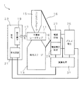
図2は、本発明の第2実施形態を示す半導体装置である半導体レーザチップ11の検査装置1の構成を示すブロック図である。本発明の第2実施形態は、電流印加手段と、測定手段と、演算処理手段とを含む半導体装置である半導体レーザチップ11の検査装置である。パルス電流を用いて検査する半導体レーザチップの検査装置である。
FIG. 2 is a block diagram showing a configuration of an
電流印加手段は、半導体装置である半導体レーザチップに電流を印加する。具体的には、パルス発生部25、電流印加部27、発光ステージ13、コンタクトプローブ15を含んで構成される。パルス発生部25は、周期およびパルス幅などのパルス条件を制御可能であり、このパルス条件のパルス信号を発生させる。電流印加部27は、パルス発生部25からのパルス信号および設定される電流値を基に半導体レーザチップ11に印加するパルス電流を生成し印加する。電流印加部27と発光ステージ13およびコンタクトプローブ15は、ケーブル16で電気的に接続されている。発光ステージ13は、半導体レーザチップ11を保持するための機構を有する。半導体レーザチップ11が高温になる場合などには、たとえばペルチェ素子などの冷却手段によって冷却してもよい。コンタクトプローブ15を、半導体レーザチップ11の入出力端子に接触させて、半導体レーザチップ検査装置1と電気的接触を取る。
The current applying means applies a current to the semiconductor laser chip that is a semiconductor device. Specifically, it includes a
測定手段は、半導体装置である半導体レーザチップ11の状態を表す光出力、端子間の電圧などの特性値を測定する。その他出力される光の波長、半導体レーザチップ11の温度などの特性値を測定することもできる。本実施の形態において、具体的には、受光部23と電流電圧測定部29を含んで構成され、電流、電圧および光出力を測定する。
The measuring means measures characteristic values such as an optical output representing the state of the semiconductor laser chip 11 which is a semiconductor device, and a voltage between terminals. Other characteristic values such as the wavelength of the output light and the temperature of the semiconductor laser chip 11 can also be measured. In the present embodiment, specifically, the
受光部23は、パルス電流が与えられた半導体レーザチップ11から発せられた光17を受光して光出力を測定する。受光部23は、光出力を測定するため半導体レーザチップ11の光出射面側に設置する。受光部23は、たとえば、受光素子19および受光回路21によって実現される。受光素子19は、受光した光を電気エネルギーに変換する素子である。受光回路21は、受光素子19からの出力を演算処理手段31へ出力するのに適したものにするための回路である。電流電圧測定部29は、半導体レーザチップ11の電流および端子間の電圧を測定する。
The
演算処理手段31は、測定手段で測定された値に基づいて、半導体装置である半導体レーザチップに次に印加する電流の電流値を演算して更新設定する。演算処理手段31は、たとえば、CPUを含んで構成されるコンピュータなどによって実現することができる。演算処理手段31は、測定された電圧、電流および光出力値から半導体レーザチップ11を評価するための値を演算する。 Based on the value measured by the measuring means, the arithmetic processing means 31 calculates and updates the current value of the current to be applied to the semiconductor laser chip that is the semiconductor device. The arithmetic processing means 31 can be realized by, for example, a computer including a CPU. The arithmetic processing means 31 calculates a value for evaluating the semiconductor laser chip 11 from the measured voltage, current and optical output value.
図3は、半導体レーザチップ11の検査方法により得られるデータを示すグラフである。 FIG. 3 is a graph showing data obtained by the inspection method of the semiconductor laser chip 11.
検査装置と電気的接触を図るため検査装置のコンタクトプローブ15を発光ステージ13に載置された半導体レーザチップ11の端子に接触させる。
In order to make electrical contact with the inspection apparatus, the
電流印加手段によって、半導体レーザチップ11に電流を印加する。半導体レーザチップ11の種類に応じて決められている発光ON時間と発光OFF時間に従って、パルス発生部25において周期およびパルス幅を設定することによって設定しておく。パルス発生部25は設定に従いパルス信号を出力する。演算処理手段31が、半導体レーザチップ11の種類に応じてパルス発生部25を制御してパルス条件を設定してもよい。
A current is applied to the semiconductor laser chip 11 by current application means. In accordance with the light emission ON time and the light emission OFF time determined according to the type of the semiconductor laser chip 11, the
測定手段により電圧および光出力などの特性値を得ることができる。また、指定した電流値が実際に出力されているかどうか確かめるため電流についても測定する。電流、電圧および光出力を測定するには、たとえば、受光回路21および電流電圧測定部29の中に、パルス発生部からのトリガタイミング信号で受光素子19などから入力されたアナログ信号をホールドして出力するサンプルホールド回路を設けて受光素子19などから入力されたアナログ信号をサンプルホールドしてアナログデジタル変換(AD変換)を行うことによって電流、電圧および光出力を測定する。
Characteristic values such as voltage and light output can be obtained by the measuring means. Also, measure the current to see if the specified current value is actually output. In order to measure the current, voltage, and optical output, for example, an analog signal input from the
この測定値に基づいて演算処理手段31は次に印加すべき電流の電流値を演算して設定する。設定された電流値に基づいて電流印加部27は半導体装置に電流を印加する。そして、再び測定手段により測定値を得る。得られた測定値に基づいて演算処理手段31は次に印加すべき電流の電流値を演算して設定する。これらの測定工程および電流値設定工程を繰返して予め定める終了条件に達した場合には、測定を終える。
Based on this measured value, the arithmetic processing means 31 calculates and sets the current value of the current to be applied next. Based on the set current value, the
検査に必要な電流値の電流を流すことができるので必要な性能を確保しつつ検査を行うことができ、検査に不要な測定を省くことができるので短時間で検査を終えることができる検査装置を提供することができる。また、半導体レーザチップ11に与えるダメージを低減することができるので、高信頼性を確保できる。 An inspection device that can pass the current of the current value necessary for inspection, can perform inspection while ensuring the necessary performance, and can omit unnecessary measurement for inspection, so that inspection can be completed in a short time Can be provided. Further, since damage to the semiconductor laser chip 11 can be reduced, high reliability can be ensured.
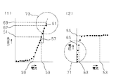
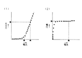
図4は、半導体レーザチップ11の性能を評価する代表的な項目を示すグラフである。図4(1)は、印加されたパルス電流に対する光出力を示すグラフであり、図4(2)は、印加されたパルス電流に対する半導体レーザチップ端子間電圧を示すグラフである。電流−電圧の立ち上がりは図4(2)に示すグラフよりも実際にはもっと急峻であり、電流の変化幅を小さくしないと電圧測定が粗くなる。 FIG. 4 is a graph showing typical items for evaluating the performance of the semiconductor laser chip 11. 4A is a graph showing the optical output with respect to the applied pulse current, and FIG. 4B is a graph showing the voltage between the semiconductor laser chip terminals with respect to the applied pulse current. The rise of the current-voltage is actually steeper than the graph shown in FIG. 4B, and the voltage measurement becomes rough unless the current change width is reduced.
半導体レーザチップ11の性能を評価する代表的な項目は、指定パワー時の電流53であるIop(mA)、指定パワー時の電圧55であるVop(V)、微分効率57η(mW/mA)、しきい値電流59Ith(mA)、最大パワー時の直線からの落ち度61であるKinkおよび指定電流時のOpen/Short判定電圧65であるVos(V)である。これらの測定項目について信頼性の高い測定をするには、それぞれの必要とされる精度などに従って、電流の変化幅をどの程度にすべきかを予め決めておくのが望ましく、規格によりこの測定項目を測定する領域の電流の変化幅は定められていることが多い。たとえば図4の点線の円で囲まれた変化が急峻な部分である第1測定領域71およびリミットぎりぎりの第2測定領域73などについては、他の領域に比べて小さな変化幅にする。
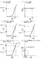
Typical items for evaluating the performance of the semiconductor laser chip 11 are Iop (mA) which is a current 53 at a specified power, Vop (V) which is a
図5は、測定項目ごとに必要な測定点を示すグラフである。必要な測定点を×印で表す。図6は、図5のグラフから必要な測定点をまとめて示すグラフである。必要な測定点を×印で表す。図7は、特性値間の対応関係および測定項目の評価値の演算に必要な点を示すグラフである。必要な測定点を×印で表す。図7(1)は、測定した全ての測定点の電流、電圧および光出力間の対応関係を示す。図7(2)は、図7(1)のうち、測定項目の評価値の演算に必要な点を示す。 FIG. 5 is a graph showing measurement points necessary for each measurement item. Necessary measurement points are represented by crosses. FIG. 6 is a graph collectively showing necessary measurement points from the graph of FIG. Necessary measurement points are represented by crosses. FIG. 7 is a graph showing points necessary for calculating the correspondence between the characteristic values and the evaluation value of the measurement item. Necessary measurement points are represented by crosses. FIG. 7 (1) shows the correspondence between the current, voltage and light output at all measured measurement points. FIG. 7 (2) shows points necessary for the calculation of the evaluation value of the measurement item in FIG. 7 (1).
実際に測定した電流、電圧、光出力値およびそれらの変化幅から演算処理手段31は、その後に印加する電流の変化幅を決める。必ずしも、パルスを加える度に電流値を変化させなくてはならないわけではなく、たとえば、測定の信頼性を高めるため、同じ値のパルスを複数回与え、その後変化させて再び変化後の同じ値のパルスを複数回与えることによって測定する方法であってもよい。 From the actually measured current, voltage, light output value, and their change width, the arithmetic processing means 31 determines the change width of the current applied thereafter. It is not always necessary to change the current value every time a pulse is applied.For example, in order to increase the reliability of measurement, a pulse having the same value is given a plurality of times, then changed and changed again. It may be a method of measuring by giving a pulse a plurality of times.
0(mA)から測定を始め、電流に対する電圧の立ち上がりをみるために、たとえば、周期が1msecで、パルスOn時間が1μsec(usec)、パルスOff時間が999μsec(usec)のパルス電流を一定の小さな変化幅(通常、0.2mA)でパルスの最大値を増大させながら、測定を行う。 In order to start the measurement from 0 (mA) and observe the rise of the voltage with respect to the current, for example, a pulse current having a period of 1 msec, a pulse On time of 1 μsec (usec), and a pulse Off time of 999 μsec (usec) is a constant small Measurement is performed while increasing the maximum value of the pulse with a change width (usually 0.2 mA).
指定電流値63に達すれば、指定電流時のOpen/Short判定電圧65であるVos(V)を測定し、異常値であれば、測定を直ちに中止する。半導体レーザチップ11の端子間電圧値がリミット電圧値以上であればコンタクトプローブ15と半導体レーザチップ11の電極がつながってないオープン不具合であると判定する。半導体レーザチップ11に正常にコンタクトされていれば、半導体レーザチップ端子間電圧は機種によっても異なるが通常約3V以上になることはなく、コンタクトプローブ15と半導体レーザチップ11の電極を接触させずに電流を流すとコンタクトプローブ15の電圧が急上昇するからである。半導体レーザチップ11の端子間電圧が指定電圧以下であればショート不具合であると判定する。ショートしていれば、半導体レーザチップ11電極端子間の電圧はほぼ0になるからである。これらの判定により接触に関する不具合がないことを確認する。
If the specified
指定電流時のOpen/Short判定電圧65であるVos(V)を測定し、正常値
であれば、指定パワー1までは、電流の変化幅を大きくすることができる。測定項目に不要な領域では、下記式(1)の最大変化可能幅を超えないことを条件に、電流値の変化幅を大きくすることができる。
The Vos (V) that is the Open /
たとえば、現時点でのパワーが0.5mWで、その機種仕様のMax微分効率57が1.0mWで、リミットパワー69が7.2mWであったとすると、最大変化可能幅として(7.2−0.5)/1.0=6.7mAにすることができる。上式で求められる最大変化可能幅まで、電流の変化幅を大きくすることができるが、指定パワー2を超えると戻り処理に時間がかかるため、この半分程度の値で変化させるのが好ましい。指定パワー1とは、微分効率を求めるための小さいほうのパワーである。指定パワー2とは、微分効率を求めるための大きいほうのパワーである。
For example, if the current power is 0.5 mW, the Max
指定パワー1を超えたら、その前の電流値に戻って、正規の変化幅(通常2.0mA)でパルス電流値を増大させることによって必要な測定項目の測定をする。微分効率57、しきい値電流59、指定パワー時の電流53、電圧55を測定するため、指定パワー1から指定パワー2までの間を、定められた正規の変化幅(通常2.0mA)で変化させる。測定した値に測定すべき値と同じ値がない場合は、その測定すべき値を含む前後の測定値から1次近似によって計算して求める。具体的には、前後の測定値から直線式を求めて測定すべき値に相当する値を計算して求める。
When the specified
指定パワー2を超えると、再びパルス電流の変化幅を大きくしてパルス電流を印加していく。半導体レーザチップ11が最大光パワー値を超えないように、現変化幅のままで2回電流値を変化させたとすると最大光パワー値67を超えると判断した点から印加するパルス電流の変化幅を小さくして、最終指定パワー67に近づいたら再び変化幅を小さくする。このとき、1ステップでリミットパワー69を超えないレベルの変化幅に設定する。たとえば、リミットパワー69が7.2mWであり、微分効率57が0.9mW/mAの特性をもつ半導体レーザチップ11を測定上最大7.0mWまで光らせる場合、(7.2−7.0)/0.9=0.22mA以下の変化幅でなければならない。電流値ならびに電圧値および光出力値がそれぞれの指定リミットであるリミット電流ならびにリミット電圧およびリミットパワー69を越えて半導体レーザチップが破壊されないように観察を行いつつ、次回の変化幅を決定する。
When the specified
指定のリミットパワー69以下で最終指定パワー67以上の領域に電流値が達したときに測定を終了する。指定電流時のOpen/Short判定電圧65であるVos以外の測定項目は、通常、測定が完了してから、測定データを基に演算して評価値を出すが、その都度計算しても良い。測定された最終指定パワー67から最大パワー時の直線からの落ち度であるKink61を求める。測定を完了した後、コンタクトプローブ15を半導体レーザチップ11から退避させる。演算処理手段31は、これらの測定データをもとに性能を評価できるようにデータ処理を行う。このデータ処理の結果を基に半導体レーザチップ11が良品であるか否かの判定を行う。
The measurement ends when the current value reaches an area where the specified limit power is 69 or less and the final specified power is 67 or more. Measurement items other than Vos, which is the Open /
本実施形態の半導体レーザチップ11の検査方法では、従来の方法で用いられる多数回印加制御を行うのではなく、半導体レーザチップ11の性能を評価するために必要な電流値に対してパルス電流の印加を行う。したがって、必要な性能の確保と処理時間の短縮を両立させることが可能となる。また、パルス電流の印加回数を減らすことができるため半導体レーザチップ11に対するダメージを低減できるので高信頼性を確保できる。 In the inspection method of the semiconductor laser chip 11 of the present embodiment, the application of the pulse current with respect to the current value necessary for evaluating the performance of the semiconductor laser chip 11 is not performed, but the multiple application control used in the conventional method is performed. Apply. Therefore, it is possible to achieve both necessary performance and reduction in processing time. In addition, since the number of pulse current applications can be reduced, damage to the semiconductor laser chip 11 can be reduced, so that high reliability can be ensured.
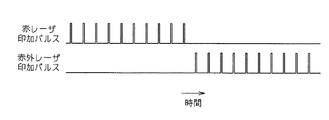
図8は本発明の第3実施形態に係る半導体レーザチップの検査方法のパルス発生タイミングを示すタイムチャートである。本発明の第3実施形態は、2つのレーザ光発生部が1つのチップにある半導体レーザチップ11を検査する方法および検査装置についての実施形態である。たとえば、1つの半導体レーザチップ11中に2つの発光点を有するモノシリックレーザ、並びに2つのレーザチップを1つのサブチップの上にダイボンドしているハイブリッドレーザなどは2つの半導体装置があるとしてよいものとする。レーザ光発生部は、必ずしも2つには限られず、2つを超える複数の場合であっても好ましく適用できる。 FIG. 8 is a time chart showing the pulse generation timing of the semiconductor laser chip inspection method according to the third embodiment of the present invention. The third embodiment of the present invention is an embodiment of a method and an inspection apparatus for inspecting a semiconductor laser chip 11 having two laser light generation units on one chip. For example, a monolithic laser having two light emission points in one semiconductor laser chip 11 and a hybrid laser in which two laser chips are die-bonded on one subchip may have two semiconductor devices. . The number of laser light generators is not necessarily limited to two, and can be preferably applied even when there are a plurality of laser light generators exceeding two.
発光ステージ13に載置された半導体レーザチップ11の2つのレーザ光発生部に電力を供給するために、各々の電極にコンタクトプローブ15を接触させる。2つのレーザ光発生部があるため、コンタクトプローブ15は、2つのレーザ光発生部用に2対ある。2つのレーザ光発生部を区別するためにそれぞれAレーザとBレーザとする。たとえば、Aレーザが赤色レーザであり、Bレーザが赤外線レーザである場合のように、異なる波長のレーザを並行して検査することができる。また、AレーザおよびBレーザが同じ波長のレーザ光を発するものであっても好ましく検査することができる。
In order to supply electric power to the two laser light generators of the semiconductor laser chip 11 mounted on the
本実施形態の測定工程では、各半導体装置に順次選択的に電流を印加する。各半導体装置に順次選択的にとは、同時に複数の半導体装置に電流を印加することなく、1つの半導体装置のみを順次選択するものとする。予めAレーザおよびBレーザに決められた発光ON時間と発光OFF時間をパルス発生部25で各々設定しておく。AレーザとBレーザの発光ON時が重ならないように設定しておくのが好ましい。本実施の形態においては、独立して2つのパルスを出力できるパルス発生部25を用いて、AレーザとBレーザに印加するパルス電流の周期を同じくし、Aレーザのパルス電流とBレーザのパルス電流の位相を一定程度ずらして、Aレーザのパルス電流のパルスON時にBレーザのパルス電流のパルスON時が重ならないような異なる位相に設定する。ここでいうパルスON時とは、パルス電流の立ち上がり時から立ち下り時の間の全ての時をいうものとする。こうすれば、簡易に、それ以降それぞれのパルスON時が重ならないようにすることができるので各レーザが同時に発光することはない。この他、AレーザとBレーザの発光ON時間が重ならないような調停手段を設けることによって、AレーザとBレーザの同時に測定する事態を回避してもよい。
In the measurement process of this embodiment, a current is selectively applied to each semiconductor device sequentially. Sequentially selecting each semiconductor device means that only one semiconductor device is sequentially selected without applying current to a plurality of semiconductor devices at the same time. The light emission ON time and the light emission OFF time determined in advance for the A laser and the B laser are respectively set by the
AレーザおよびBレーザにパルス電流を印加して各々のパルスON時の電流並びに電圧および光出力を測定する。AレーザおよびBレーザから照射される光を受光できる位置に配置された1つの受光素子19でAレーザおよびBレーザから照射される光を受光する。受光部23および電流電圧測定部29の中に設けられたサンプルホールド回路から出力されるアナログ信号をAD変換して得られた測定結果が演算処理手段31に入力される。パルス発生部25において発せられるどちらのレーザ用のパルスであるかを識別できる信号によって演算処理手段31はどちらのレーザの測定を行ったかを区別して測定結果を演算処理する。このように、各半導体装置に順次選択的に電流を印加して半導体装置の特性を測定するので、各半導体装置毎に特性値測定装置を設けることなく測定することができる。必ずしも、1つの受光素子19で複数の発光部からの光を受光しなければならないわけではなく、複数の受光素子を用いてそれぞれ測定してもよい。
A pulse current is applied to the A laser and the B laser, and the current, voltage, and optical output when each pulse is ON are measured. The light irradiated from the A laser and the B laser is received by one
Aレーザの測定およびBレーザの測定については、前述の1つの半導体装置を検査する方法と同様の方法により行う。各レーザ毎に、指定パワー時の電流53であるIop(mA)、指定パワー時の電圧55であるVop(V)、指定パワー2と指定パワー1との傾きである微分効率57η(mW/mA)、指定パワー2と指定パワー1の2点からなる直線と電流軸との交点であるしきい値電流59であるIth(mA)、最大パワー時の直線からの落ち度61であるKinkおよび指定電流時のOpen/Short判定電圧65であるVos(V)などの測定項目について評価するために電流値ならびに電圧値および光出力値などの特性値を測定する。
The measurement of the A laser and the measurement of the B laser are performed by a method similar to the method for inspecting one semiconductor device described above. For each laser, Iop (mA) which is a current 53 at a specified power, Vop (V) which is a
設定工程では、各半導体装置毎に測定された特性値に基づいて、各々次に印加する電流の電流値を演算して更新設定する。AレーザとBレーザの波長が異なる場合、AレーザとBレーザの特性が異なるので、指定パワー51、指定電流63、最終指定パワー67およびリミットパワー69を演算処理手段31において各々設定しておく。演算処理手段31は、AレーザとBレーザの電流値ならびに電圧値および光出力値がそれぞれの指定リミットを越えて半導体レーザチップが破壊されないように観察を行いつつ、各々のレーザに次に印加する電流の変化幅を決定する。
In the setting step, the current value of the current to be applied next is calculated and updated based on the characteristic value measured for each semiconductor device. When the wavelengths of the A laser and the B laser are different, the characteristics of the A laser and the B laser are different. Therefore, the designated
各々のレーザのリミットパワー69以下で各々のレーザの最終指定パワー67以上の領域に電流値が達したときに各々の測定を終了する。測定を終了した後、コンタクトプローブ15を半導体レーザチップ11から退避させる。演算処理手段31は、これらの測定データを基に性能を評価できるようにデータ処理を行う。さらに、演算処理手段31は、このデータ処理の結果を基に半導体レーザチップ11が良品であるか否かの判定を行う。Aレーザを測定し終わってからBレーザを測定することにより測定する従来技術に比べてAレーザの測定とBレーザの測定を並列に実行するので、複数の半導体装置を全部検査し終えるまでに要する実時間を短縮することができる。
Each measurement is terminated when the current value reaches a region where the laser has a limit power of 69 or less and a final specified power of 67 or more for each laser. After the measurement is completed, the
1 半導体レーザチップ検査装置
11 半導体レーザチップ
13 発光ステージ
15 コンタクトプローブ
16 ケーブル
17 光
19 受光素子
21 受光回路
23 受光部
25 パルス発生部
27 電流印加部
29 電流電圧測定部
31 演算処理手段
51 指定パワー
53 指定パワー時の電流
55 指定パワー時の電圧
57 微分効率
59 しきい値電流
61 最終指定パワー時の直線からの落ち度
63 指定電流値
65 指定電流時のOPEN/SHORT判定電圧
67 最終指定パワー
69 リミットパワー
71 第1測定領域
73 第2測定領域
DESCRIPTION OF
Claims (12)
設定される電流値の電流を半導体装置に印加して、半導体装置の状態を表す特性値を測定する測定工程と、
測定工程で測定された特性値に基づいて、次に半導体装置に印加する電流の電流値を演算して更新設定する設定工程と、
測定工程および設定工程を、予め定める条件を満たすまで、繰返す繰返し工程とを含むことを特徴とする半導体装置の検査方法。 A semiconductor device inspection method for measuring a characteristic value representing a state of a semiconductor device when a current having a plurality of current values is applied to the semiconductor device,
A measuring step of applying a current of a set current value to the semiconductor device and measuring a characteristic value representing a state of the semiconductor device;
Based on the characteristic value measured in the measurement step, a setting step for calculating and updating the current value of the current to be applied to the semiconductor device next,
A method for inspecting a semiconductor device, comprising: repeating a measurement process and a setting process until a predetermined condition is satisfied.
前記測定工程では、各半導体装置に順次選択的に電流を印加することを特徴とする請求項1記載の半導体装置の検査方法。 A method for inspecting a semiconductor device that executes inspection of a plurality of semiconductor devices in parallel,
2. The method for inspecting a semiconductor device according to claim 1, wherein in the measuring step, a current is selectively applied to each semiconductor device sequentially.
前記設定工程では、測定項目を評価するのに必要な測定領域以外の測定領域を測定する際、測定項目を評価する際のパルス電流の最大パルス電流値間の変化幅を超えて、かつ、前記半導体レーザチップのリミットパワーを前記半導体レーザチップの現時点でのパワーで減算してこの減算値を前記半導体レーザチップのMax微分効率で除算した値を超えないパルス電流の最大パルス電流値間の変化幅である電流値を設定することを特徴とする請求項5に記載の半導体装置の検査方法。 A method for inspecting a semiconductor device that measures a light output value and a voltage value by applying a pulse current,
In the setting step, when measuring a measurement region other than the measurement region necessary for evaluating the measurement item, exceeding the change width between the maximum pulse current values of the pulse current when evaluating the measurement item, and the above The change width between the maximum pulse current values of the pulse current not exceeding the value obtained by subtracting the limit power of the semiconductor laser chip by the current power of the semiconductor laser chip and dividing this subtracted value by the Max differential efficiency of the semiconductor laser chip 6. The method of inspecting a semiconductor device according to claim 5, wherein the current value is set.
半導体装置の状態を表す特性値を測定する測定手段と、
測定手段で測定された特性値に基づいて、次に半導体装置に印加する電流の電流値を演算して更新設定する演算処理手段とを含むことを特徴とする半導体装置の検査装置。 Current application means for applying a current to the semiconductor device;
Measuring means for measuring characteristic values representing the state of the semiconductor device;
An inspection apparatus for a semiconductor device, comprising: arithmetic processing means for calculating and updating a current value of a current to be applied to the semiconductor device next based on the characteristic value measured by the measuring means.
前記電流印加手段では、各半導体装置に順次選択的に電流を印加することを特徴とする請求項7記載の半導体装置の検査装置。 A semiconductor device inspection apparatus that performs inspection of a plurality of semiconductor devices in parallel,
8. The semiconductor device inspection apparatus according to claim 7, wherein the current application means selectively applies a current to each semiconductor device sequentially.
前記演算処理手段は、測定項目を評価するのに必要な測定領域以外の測定領域を、測定項目を評価する際のパルス電流の最大パルス電流値間の変化幅を超えて、かつ、前記半導体レーザチップのリミットパワーを前記半導体レーザチップの現時点でのパワーで減算してこの減算値を前記半導体レーザチップのMax微分効率で除算した値を超えないパルス電流の最大パルス電流値間の変化幅である電流値を設定することを特徴とする請求項11に記載の半導体装置の検査装置。 A semiconductor device inspection apparatus that measures a light output value and a voltage value by applying a pulse current,
The arithmetic processing means has a measurement region other than the measurement region necessary for evaluating the measurement item, exceeding a change width between the maximum pulse current values of the pulse current when evaluating the measurement item, and the semiconductor laser. This is the change width between the maximum pulse current values of the pulse current that does not exceed the value obtained by subtracting the limit power of the chip by the current power of the semiconductor laser chip and dividing this subtracted value by the Max differential efficiency of the semiconductor laser chip. 12. The semiconductor device inspection apparatus according to claim 11, wherein a current value is set.
Priority Applications (1)
| Application Number | Priority Date | Filing Date | Title |
|---|---|---|---|
| JP2004105913A JP2005294449A (en) | 2004-03-31 | 2004-03-31 | Semiconductor device inspection method and inspection apparatus |
Applications Claiming Priority (1)
| Application Number | Priority Date | Filing Date | Title |
|---|---|---|---|
| JP2004105913A JP2005294449A (en) | 2004-03-31 | 2004-03-31 | Semiconductor device inspection method and inspection apparatus |
Publications (1)
| Publication Number | Publication Date |
|---|---|
| JP2005294449A true JP2005294449A (en) | 2005-10-20 |
Family
ID=35327064
Family Applications (1)
| Application Number | Title | Priority Date | Filing Date |
|---|---|---|---|
| JP2004105913A Pending JP2005294449A (en) | 2004-03-31 | 2004-03-31 | Semiconductor device inspection method and inspection apparatus |
Country Status (1)
| Country | Link |
|---|---|
| JP (1) | JP2005294449A (en) |
Cited By (9)
| Publication number | Priority date | Publication date | Assignee | Title |
|---|---|---|---|---|
| WO2009113183A1 (en) * | 2008-03-11 | 2009-09-17 | 株式会社東京精密 | Multichip prober |
| JP2010067659A (en) * | 2008-09-09 | 2010-03-25 | Arufakusu Kk | Inspection device and inspection method for semiconductor laser |
| JP2011179937A (en) * | 2010-03-01 | 2011-09-15 | Hirayama Seisakusho:Kk | Led life testing method and apparatus |
| JP2016191560A (en) * | 2015-03-30 | 2016-11-10 | 国立大学法人京都工芸繊維大学 | Power supply device and current-voltage characteristic measuring device |
| JP2019047117A (en) * | 2017-08-31 | 2019-03-22 | 日亜化学工業株式会社 | Method for manufacturing light-emitting device and light-emitting device |
| JPWO2019220832A1 (en) * | 2018-05-18 | 2021-07-01 | パナソニックIpマネジメント株式会社 | Direct diode laser type laser oscillator and failure diagnosis method for laser oscillator |
| CN114664704A (en) * | 2022-03-18 | 2022-06-24 | 东莞市中麒光电技术有限公司 | LED chip screening method and display screen |
| CN117074836A (en) * | 2023-10-12 | 2023-11-17 | 成都明夷电子科技有限公司 | Laser detection method, detector, electronic equipment and storage medium |
| JP7609339B1 (en) * | 2024-05-24 | 2025-01-07 | 三菱電機株式会社 | Inspection device and semiconductor device manufacturing method |
-
2004
- 2004-03-31 JP JP2004105913A patent/JP2005294449A/en active Pending
Cited By (13)
| Publication number | Priority date | Publication date | Assignee | Title |
|---|---|---|---|---|
| WO2009113183A1 (en) * | 2008-03-11 | 2009-09-17 | 株式会社東京精密 | Multichip prober |
| JP2010067659A (en) * | 2008-09-09 | 2010-03-25 | Arufakusu Kk | Inspection device and inspection method for semiconductor laser |
| JP2011179937A (en) * | 2010-03-01 | 2011-09-15 | Hirayama Seisakusho:Kk | Led life testing method and apparatus |
| JP2016191560A (en) * | 2015-03-30 | 2016-11-10 | 国立大学法人京都工芸繊維大学 | Power supply device and current-voltage characteristic measuring device |
| JP2019047117A (en) * | 2017-08-31 | 2019-03-22 | 日亜化学工業株式会社 | Method for manufacturing light-emitting device and light-emitting device |
| US12176674B2 (en) | 2018-05-18 | 2024-12-24 | Panasonic Intellectual Property Management Co., Ltd. | Laser oscillation device for direct-diode laser method and failure diagnosis method for laser oscillation device |
| JPWO2019220832A1 (en) * | 2018-05-18 | 2021-07-01 | パナソニックIpマネジメント株式会社 | Direct diode laser type laser oscillator and failure diagnosis method for laser oscillator |
| JP7329733B2 (en) | 2018-05-18 | 2023-08-21 | パナソニックIpマネジメント株式会社 | Direct diode laser type laser oscillation device and failure diagnosis method for laser oscillation device |
| CN114664704A (en) * | 2022-03-18 | 2022-06-24 | 东莞市中麒光电技术有限公司 | LED chip screening method and display screen |
| CN117074836B (en) * | 2023-10-12 | 2024-03-12 | 成都明夷电子科技有限公司 | Laser detection method, detector, electronic equipment and storage medium |
| CN117074836A (en) * | 2023-10-12 | 2023-11-17 | 成都明夷电子科技有限公司 | Laser detection method, detector, electronic equipment and storage medium |
| JP7609339B1 (en) * | 2024-05-24 | 2025-01-07 | 三菱電機株式会社 | Inspection device and semiconductor device manufacturing method |
| WO2025243512A1 (en) * | 2024-05-24 | 2025-11-27 | 三菱電機株式会社 | Probe, inspection apparatus, and method for producing semiconductor device |
Similar Documents
| Publication | Publication Date | Title |
|---|---|---|
| US11187747B2 (en) | Inspection system and malfunction analysis/prediction method for inspection system | |
| TW201305552A (en) | Method and apparatus for verifying a light emitting semiconductor device using photoluminescence imaging | |
| US7006212B2 (en) | Electrical circuit conductor inspection | |
| JP2005294449A (en) | Semiconductor device inspection method and inspection apparatus | |
| JPH11330179A (en) | Method for measuring minority carrier diffusion length and minority carrier lifetime in semiconductor devices | |
| WO2004040326A1 (en) | Defect analyzing device for semiconductor integrated circuits, system therefor, and detection method | |
| JP4136832B2 (en) | Inspection method and inspection apparatus for semiconductor laser diode chip | |
| KR101165385B1 (en) | Optical inspection method and apparatus using light-guide electricity probe | |
| KR100944535B1 (en) | Apparatus and method for inspecting solder bump formation and transition state using electron beam in wafer bumping process | |
| CN111512169B (en) | Light measurement method, light measurement device, and storage medium for storing light measurement program | |
| JP2010261769A (en) | Printed circuit board inspection apparatus and inspection method | |
| KR101153339B1 (en) | Method for inspecting semiconductor light emitting device | |
| JP2005032760A (en) | Method for inspecting defect of semiconductor device | |
| US6677172B1 (en) | On-wafer burn-in of semiconductor devices using thermal rollover | |
| JP2022191643A (en) | Method for manufacturing surface emitting laser, method for inspecting surface emitting laser, and inspection apparatus for surface emitting laser | |
| JP2015076583A (en) | Photoelectric conversion element evaluation device | |
| JP3287332B2 (en) | Device for detecting disconnection failure of semiconductor integrated circuit and method of detecting disconnection failure thereof | |
| JP7514215B2 (en) | Inspection method, semiconductor device manufacturing method, inspection device, inspection system, program, and storage medium | |
| JP2007155640A (en) | Method and system for inspecting integrated circuit | |
| KR102822963B1 (en) | Inspection device, inspection method and program for inspection device | |
| Schmid et al. | Transient thermal analysis for VCSEL Diodes | |
| US20260029459A1 (en) | Inspection device and inspection method | |
| JPH02194541A (en) | Optical prober | |
| JP2648947B2 (en) | Inspection equipment for semiconductor devices | |
| KR20130112680A (en) | Led chip testing apparatus |
Legal Events
| Date | Code | Title | Description |
|---|---|---|---|
| A621 | Written request for application examination |
Free format text: JAPANESE INTERMEDIATE CODE: A621 Effective date: 20060125 |
|
| A977 | Report on retrieval |
Free format text: JAPANESE INTERMEDIATE CODE: A971007 Effective date: 20090907 |
|
| A131 | Notification of reasons for refusal |
Free format text: JAPANESE INTERMEDIATE CODE: A131 Effective date: 20090915 |
|
| A02 | Decision of refusal |
Free format text: JAPANESE INTERMEDIATE CODE: A02 Effective date: 20100202 |