JP2005294441A - Element mounting board and semiconductor device employing it - Google Patents
Element mounting board and semiconductor device employing it Download PDFInfo
- Publication number
- JP2005294441A JP2005294441A JP2004105764A JP2004105764A JP2005294441A JP 2005294441 A JP2005294441 A JP 2005294441A JP 2004105764 A JP2004105764 A JP 2004105764A JP 2004105764 A JP2004105764 A JP 2004105764A JP 2005294441 A JP2005294441 A JP 2005294441A
- Authority
- JP
- Japan
- Prior art keywords
- resist layer
- element mounting
- resin film
- solder resist
- mounting substrate
- Prior art date
- Legal status (The legal status is an assumption and is not a legal conclusion. Google has not performed a legal analysis and makes no representation as to the accuracy of the status listed.)
- Pending
Links
Images


Classifications
-
- H—ELECTRICITY
- H01—ELECTRIC ELEMENTS
- H01L—SEMICONDUCTOR DEVICES NOT COVERED BY CLASS H10
- H01L2224/00—Indexing scheme for arrangements for connecting or disconnecting semiconductor or solid-state bodies and methods related thereto as covered by H01L24/00
- H01L2224/01—Means for bonding being attached to, or being formed on, the surface to be connected, e.g. chip-to-package, die-attach, "first-level" interconnects; Manufacturing methods related thereto
- H01L2224/02—Bonding areas; Manufacturing methods related thereto
- H01L2224/04—Structure, shape, material or disposition of the bonding areas prior to the connecting process
- H01L2224/05—Structure, shape, material or disposition of the bonding areas prior to the connecting process of an individual bonding area
- H01L2224/0554—External layer
- H01L2224/0555—Shape
- H01L2224/05552—Shape in top view
- H01L2224/05554—Shape in top view being square
-
- H—ELECTRICITY
- H01—ELECTRIC ELEMENTS
- H01L—SEMICONDUCTOR DEVICES NOT COVERED BY CLASS H10
- H01L2224/00—Indexing scheme for arrangements for connecting or disconnecting semiconductor or solid-state bodies and methods related thereto as covered by H01L24/00
- H01L2224/01—Means for bonding being attached to, or being formed on, the surface to be connected, e.g. chip-to-package, die-attach, "first-level" interconnects; Manufacturing methods related thereto
- H01L2224/10—Bump connectors; Manufacturing methods related thereto
- H01L2224/15—Structure, shape, material or disposition of the bump connectors after the connecting process
- H01L2224/16—Structure, shape, material or disposition of the bump connectors after the connecting process of an individual bump connector
- H01L2224/161—Disposition
- H01L2224/16151—Disposition the bump connector connecting between a semiconductor or solid-state body and an item not being a semiconductor or solid-state body, e.g. chip-to-substrate, chip-to-passive
- H01L2224/16221—Disposition the bump connector connecting between a semiconductor or solid-state body and an item not being a semiconductor or solid-state body, e.g. chip-to-substrate, chip-to-passive the body and the item being stacked
- H01L2224/16225—Disposition the bump connector connecting between a semiconductor or solid-state body and an item not being a semiconductor or solid-state body, e.g. chip-to-substrate, chip-to-passive the body and the item being stacked the item being non-metallic, e.g. insulating substrate with or without metallisation
-
- H—ELECTRICITY
- H01—ELECTRIC ELEMENTS
- H01L—SEMICONDUCTOR DEVICES NOT COVERED BY CLASS H10
- H01L2224/00—Indexing scheme for arrangements for connecting or disconnecting semiconductor or solid-state bodies and methods related thereto as covered by H01L24/00
- H01L2224/01—Means for bonding being attached to, or being formed on, the surface to be connected, e.g. chip-to-package, die-attach, "first-level" interconnects; Manufacturing methods related thereto
- H01L2224/42—Wire connectors; Manufacturing methods related thereto
- H01L2224/44—Structure, shape, material or disposition of the wire connectors prior to the connecting process
- H01L2224/45—Structure, shape, material or disposition of the wire connectors prior to the connecting process of an individual wire connector
- H01L2224/45001—Core members of the connector
- H01L2224/45099—Material
- H01L2224/451—Material with a principal constituent of the material being a metal or a metalloid, e.g. boron (B), silicon (Si), germanium (Ge), arsenic (As), antimony (Sb), tellurium (Te) and polonium (Po), and alloys thereof
- H01L2224/45138—Material with a principal constituent of the material being a metal or a metalloid, e.g. boron (B), silicon (Si), germanium (Ge), arsenic (As), antimony (Sb), tellurium (Te) and polonium (Po), and alloys thereof the principal constituent melting at a temperature of greater than or equal to 950°C and less than 1550°C
- H01L2224/45144—Gold (Au) as principal constituent
-
- H—ELECTRICITY
- H01—ELECTRIC ELEMENTS
- H01L—SEMICONDUCTOR DEVICES NOT COVERED BY CLASS H10
- H01L2224/00—Indexing scheme for arrangements for connecting or disconnecting semiconductor or solid-state bodies and methods related thereto as covered by H01L24/00
- H01L2224/01—Means for bonding being attached to, or being formed on, the surface to be connected, e.g. chip-to-package, die-attach, "first-level" interconnects; Manufacturing methods related thereto
- H01L2224/42—Wire connectors; Manufacturing methods related thereto
- H01L2224/47—Structure, shape, material or disposition of the wire connectors after the connecting process
- H01L2224/48—Structure, shape, material or disposition of the wire connectors after the connecting process of an individual wire connector
- H01L2224/481—Disposition
- H01L2224/48151—Connecting between a semiconductor or solid-state body and an item not being a semiconductor or solid-state body, e.g. chip-to-substrate, chip-to-passive
- H01L2224/48221—Connecting between a semiconductor or solid-state body and an item not being a semiconductor or solid-state body, e.g. chip-to-substrate, chip-to-passive the body and the item being stacked
- H01L2224/48225—Connecting between a semiconductor or solid-state body and an item not being a semiconductor or solid-state body, e.g. chip-to-substrate, chip-to-passive the body and the item being stacked the item being non-metallic, e.g. insulating substrate with or without metallisation
- H01L2224/48227—Connecting between a semiconductor or solid-state body and an item not being a semiconductor or solid-state body, e.g. chip-to-substrate, chip-to-passive the body and the item being stacked the item being non-metallic, e.g. insulating substrate with or without metallisation connecting the wire to a bond pad of the item
-
- H—ELECTRICITY
- H01—ELECTRIC ELEMENTS
- H01L—SEMICONDUCTOR DEVICES NOT COVERED BY CLASS H10
- H01L2924/00—Indexing scheme for arrangements or methods for connecting or disconnecting semiconductor or solid-state bodies as covered by H01L24/00
- H01L2924/19—Details of hybrid assemblies other than the semiconductor or other solid state devices to be connected
- H01L2924/191—Disposition
- H01L2924/19101—Disposition of discrete passive components
- H01L2924/19105—Disposition of discrete passive components in a side-by-side arrangement on a common die mounting substrate
Landscapes
- Production Of Multi-Layered Print Wiring Board (AREA)
Abstract
Description
本発明は、素子搭載基板およびそれを用いた半導体装置に関するものである。 The present invention relates to an element mounting substrate and a semiconductor device using the same.
携帯電話、PDA、DVC、DSCといったポータブルエレクトロニクス機器の高機能化が加速するなか、こうした製品が市場で受け入れられるためには小型・軽量化が必須となっており、その実現のために高集積のシステムLSIが求められている。一方、これらのエレクトロニクス機器に対しては、より使い易く便利なものが求められており、機器に使用されるLSIに対し、高機能化、高性能化が要求されている。このため、LSIチップの高集積化にともないそのI/O数が増大する一方でパッケージ自体の小型化要求も強く、これらを両立させるために、半導体部品の高密度な基板実装に適合した半導体パッケージの開発が強く求められている。こうした要求に対応するため、CSP(Chip Size Package)と呼ばれるパッケージ技術が種々開発されている。 As portable electronic devices such as mobile phones, PDAs, DVCs, and DSCs are accelerating their functions, miniaturization and weight reduction are essential for their acceptance in the market. There is a need for a system LSI. On the other hand, these electronic devices are required to be easier to use and convenient, and higher functionality and higher performance are required for LSIs used in the devices. For this reason, as the number of I / Os increases with higher integration of LSI chips, there is a strong demand for miniaturization of the package itself. In order to achieve both of these, a semiconductor package suitable for high-density board mounting of semiconductor components Development is strongly demanded. In order to meet such demands, various package technologies called CSP (Chip Size Package) have been developed.
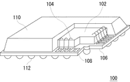
こうしたパッケージの例として、BGA(Ball Grid Array)が知られている。BGAは、パッケージ用基板の上に半導体チップを実装し、それを樹脂モールディングした後、反対側の面に外部端子としてハンダボールをエリア状に形成したものである。BGAでは、実装エリアが面で達成されるので、パッケージを比較的容易に小型化することができる。また、回路基板側でも狭ピッチ対応とする必要がなく、高精度な実装技術も不要となるので、BGAを用いると、パッケージコストが多少高い場合でもトータルな実装コストとしては低減することが可能となる。 As an example of such a package, BGA (Ball Grid Array) is known. In the BGA, a semiconductor chip is mounted on a package substrate, resin-molded, and then solder balls are formed in an area as external terminals on the opposite surface. In BGA, since the mounting area is achieved in terms of surface, the package can be reduced in size relatively easily. In addition, it is not necessary to support narrow pitches on the circuit board side, and high-precision mounting technology is not required. Therefore, if BGA is used, the total mounting cost can be reduced even if the package cost is somewhat high. Become.
図12は、一般的なBGAの概略構成を示す図である。BGA100は、ガラスエポキシ基板106上に、接着層108を介してLSIチップ102が搭載された構造を有する。LSIチップ102は封止樹脂110によってモールドされている。LSIチップ102とガラスエポキシ基板106とは、金属線104により電気的に接続されている。ガラスエポキシ基板106の裏面には、半田ボール112がアレイ状に配列されている。この半田ボール112を介して、BGA100がプリント配線基板に実装される。
FIG. 12 is a diagram showing a schematic configuration of a general BGA. The BGA 100 has a structure in which an
特許文献1には、他のCSPの例が記載されている。同公報記載には、高周波用LSIを搭載するシステム・イン・パッケージが開示されている。このパッケージは、ベース基板上に、多層配線構造が形成され、その上に高周波用LSIをはじめとする半導体素子が形成されている。多層配線構造は、コア基板、絶縁樹脂層付銅箔やソルダーレジスト層などが積層された構造となっている。 Patent Document 1 describes another example of CSP. The publication discloses a system-in-package in which a high-frequency LSI is mounted. In this package, a multilayer wiring structure is formed on a base substrate, and semiconductor elements such as a high frequency LSI are formed thereon. The multilayer wiring structure has a structure in which a core substrate, a copper foil with an insulating resin layer, a solder resist layer, and the like are laminated.
上記公報記載の技術をはじめ、システム・イン・パッケージに用いられるソルダーレジスト層は、多層配線構造の最上層に位置するため、高い加工性が要求される。また、ソルダーレジスト層の表面には、ベアチップなどの半導体素子が直接搭載されるため、吸湿特性や密着性についても高い性能が要求される。また、ソルダーレジスト層は、その層内に埋設される配線パターンの配線間絶縁膜としての役割を果たすため、寄生容量の低減が要求される。 Since the solder resist layer used in the system-in-package including the technology described in the above publication is located in the uppermost layer of the multilayer wiring structure, high workability is required. Further, since a semiconductor element such as a bare chip is directly mounted on the surface of the solder resist layer, high performance is required for moisture absorption characteristics and adhesion. Further, since the solder resist layer plays a role as an inter-wiring insulating film of a wiring pattern embedded in the layer, a reduction in parasitic capacitance is required.
また、パッケージの微細化の要求により、ソルダーレジスト層の薄膜化が求められる。 In addition, due to the demand for miniaturization of packages, it is required to make the solder resist layer thinner.
本発明は上記事情に鑑みなされたものであって、その目的とするところは、信頼性が高く、かつ小型化された素子搭載基板を提供することにある。 The present invention has been made in view of the above circumstances, and an object of the present invention is to provide a highly reliable and miniaturized element mounting substrate.
本発明によれば、素子を搭載するための素子搭載基板であって、基材と、該基材上に設けられた絶縁膜と、該絶縁膜上に設けられたソルダーレジスト層とを含み、ソルダーレジスト層は、カルド型ポリマーを含むことを特徴とする素子搭載基板が提供される。 According to the present invention, an element mounting substrate for mounting an element includes a base material, an insulating film provided on the base material, and a solder resist layer provided on the insulating film, An element mounting substrate is provided in which the solder resist layer contains a cardo type polymer.
本発明によれば、ソルダーレジスト層はカルド型ポリマーを含むことによって、ソルダーレジスト層の解像度および吸湿特性などの諸特性を向上させることができる。また、ソルダーレジスト層を薄膜化することができる。したがって、信頼性が高く、かつ小型化された素子搭載基板を提供することができる。 According to the present invention, when the solder resist layer contains a cardo type polymer, it is possible to improve various characteristics such as resolution and moisture absorption characteristics of the solder resist layer. Further, the solder resist layer can be thinned. Therefore, it is possible to provide a highly reliable and miniaturized element mounting substrate.
また、ソルダーレジスト層に素子を接続する配線が設けられていてもよい。 Moreover, the wiring which connects an element to a soldering resist layer may be provided.
また、ソルダーレジスト層のガラス転移温度が180℃以上220℃以下であり、ソルダーレジスト層の周波数1MHzの交流電界を印加した場合の誘電正接が0.001以上0.04以下であってもよい。 Further, the glass transition temperature of the solder resist layer may be 180 ° C. or higher and 220 ° C. or lower, and the dielectric loss tangent may be 0.001 or higher and 0.04 or lower when an AC electric field having a frequency of 1 MHz is applied to the solder resist layer.
また、ソルダーレジスト層のガラス転移温度以下の領域における線膨張係数が50ppm/℃以上80ppm/℃以下であってもよい。 Further, the linear expansion coefficient in the region below the glass transition temperature of the solder resist layer may be 50 ppm / ° C. or more and 80 ppm / ° C. or less.
本発明によれば、上記特徴を有する素子搭載基板と、該素子搭載基板に搭載されている半導体素子とを備えることを特徴とする半導体装置が提供される。 According to the present invention, there is provided a semiconductor device comprising an element mounting substrate having the above characteristics and a semiconductor element mounted on the element mounting substrate.
本発明によれば、信頼性が高く、かつ、小型化された素子搭載基板を備えることにより、信頼性が高く、かつ、小型化された半導体装置を提供することができる。 According to the present invention, a highly reliable and miniaturized semiconductor device can be provided by providing a highly reliable and miniaturized element mounting substrate.
なお、絶縁膜は、単層絶縁膜でも多層絶縁膜でもよいものとする。 Note that the insulating film may be a single-layer insulating film or a multilayer insulating film.
なお、本発明において、素子搭載基板とは、LSIチップやICチップなどの半導体素子を搭載するための基板を意味する。たとえば、後述するISB(登録商標)構造におけるインターポーザー基板などが挙げられる。また、素子搭載基板は、シリコン基板などの剛性を有するコア基板を備えてもよいが、コア基板を有さず、絶縁樹脂膜からなる多層絶縁膜を備えるコアレス構造であってもよい。 In the present invention, the element mounting substrate means a substrate on which a semiconductor element such as an LSI chip or an IC chip is mounted. For example, an interposer substrate in an ISB (registered trademark) structure to be described later can be used. The element mounting substrate may include a rigid core substrate such as a silicon substrate, but may have a coreless structure including a multilayer insulating film made of an insulating resin film without the core substrate.
本発明によれば、信頼性が高く、かつ小型化された素子搭載基板を提供することができる。 According to the present invention, it is possible to provide a highly reliable and miniaturized element mounting substrate.
以下、本発明の実施の形態について説明するが、その前に、実施の形態で採用するISB構造について説明する。ISB(Integrated System in Board;登録商標)は、本出願人により開発された独自のパッケージである。ISBは、半導体ベアチップを中心とする電子回路のパッケージングにおいて、銅による配線パターンを持ちながら回路部品を支持するためのコア(基材)を使用しない独自のコアレスシステム・イン・パッケージである。 Hereinafter, an embodiment of the present invention will be described, but before that, an ISB structure employed in the embodiment will be described. ISB (Integrated System in Board; registered trademark) is a unique package developed by the present applicant. ISB is a unique coreless system-in-package that does not use a core (base material) for supporting circuit components while having a wiring pattern made of copper in packaging of electronic circuits centering on semiconductor bare chips.
図1はISBの一例を示す概略構成図である。ここではISBの全体構造をわかりやすくするため、単一の配線層のみ示しているが、実際には、複数の配線層が積層した構造となっている。このISBでは、LSIベアチップ201、Trベアチップ202およびチップCR203が銅パターン205からなる配線により結線された構造となっている。LSIベアチップ201は、裏面に半田ボール208が設けられた引き出し電極や配線に対し、金線ボンディング204により導通されている。LSIベアチップ201の直下には、導電性ペースト206が設けられ、これを介してISBがプリント配線基板に実装される。ISB全体はエポキシ樹脂などからなる樹脂パッケージ207により封止された構造となっている。
FIG. 1 is a schematic configuration diagram showing an example of an ISB. Here, only a single wiring layer is shown for easy understanding of the entire structure of the ISB, but in actuality, a structure in which a plurality of wiring layers are laminated is shown. This ISB has a structure in which an
このパッケージによれば、以下の利点が得られる。
(i)コアレスで実装できるため、トランジスタ、IC、LSIの小型・薄型化を実現できる。
(ii)トランジスタからシステムLSI、さらにチップタイプのコンデンサや抵抗を回路形成し、パッケージングすることができるため、高度なSIP(System in Package)を実現できる。
(iii)現有の半導体素子を組合せできるため、システムLSIを短期間に開発できる。
(iv)半導体ベアチップが直下の銅材に直接マウントされており、良好な放熱性を得ることができる。
(v)回路配線が銅材でありコア材がないため、低誘電率の回路配線となり、高速データ転送や高周波回路で優れた特性を発揮する。
(vi)電極がパッケージの内部に埋め込まれる構造のため、電極材料のパーティクルコンタミの発生を抑制できる。
(vii)パッケージサイズはフリーであり、1個あたりの廃材を64ピンのSQFPパッケージと比較すると、約1/10の量となるため、環境負荷を低減できる。
(viii)部品を載せるプリント回路基板から、機能の入った回路基板へと、新しい概念のシステム構成を実現できる。
(ix)ISBのパターン設計は、プリント回路基板のパターン設計と同じように容易であり、セットメーカーのエンジニアが自ら設計できる。
According to this package, the following advantages are obtained.
(i) Since it can be mounted corelessly, it is possible to reduce the size and thickness of transistors, ICs and LSIs.
(ii) Since a circuit can be formed by forming a circuit from a transistor to a system LSI, and further a chip type capacitor and resistor, an advanced SIP (System in Package) can be realized.
(iii) Since existing semiconductor elements can be combined, a system LSI can be developed in a short time.
(iv) The semiconductor bare chip is directly mounted on the copper material directly below, and good heat dissipation can be obtained.
(v) Since the circuit wiring is made of copper and has no core material, the circuit wiring has a low dielectric constant and exhibits excellent characteristics in high-speed data transfer and high-frequency circuits.
(vi) Since the electrode is embedded in the package, the generation of particle contamination of the electrode material can be suppressed.
(vii) The package size is free, and the amount of waste per package is about 1/10 of the amount of SQFP package with 64 pins, so the environmental load can be reduced.
(viii) A new concept system configuration can be realized from a printed circuit board on which components are placed to a circuit board with functions.
(ix) ISB pattern design is as easy as printed circuit board pattern design, and can be designed by set manufacturer engineers.
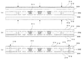
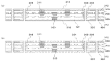
次にISBの製造プロセス上のメリットについて説明する。図2は、従来のCSPおよび本発明に係るISBの製造プロセスの対比図である。図2(B)は、従来のCSPの製造プロセスを示す。はじめにベース基板上にフレームを形成し、各フレームに区画された素子形成領域にチップが実装される。その後、各素子について熱硬化性樹脂によりパッケージが設けられ、その後、素子毎に金型を利用して打ち抜きを行う。最終工程の打ち抜きでは、モールド樹脂およびベース基板が同時に切断されるようになっており、切断面における表面荒れなどが問題になる。また打ち抜きを終わった後の廃材が多量に生じるため、環境負荷の点で課題を有していた。 Next, advantages of the ISB manufacturing process will be described. FIG. 2 is a comparison diagram of manufacturing processes of a conventional CSP and an ISB according to the present invention. FIG. 2B shows a conventional CSP manufacturing process. First, a frame is formed on a base substrate, and a chip is mounted in an element formation region partitioned by each frame. Thereafter, a package is provided for each element by a thermosetting resin, and thereafter, punching is performed using a die for each element. In stamping in the final process, the mold resin and the base substrate are cut at the same time, and surface roughness on the cut surface becomes a problem. In addition, since a large amount of waste material is generated after punching, there is a problem in terms of environmental load.
一方、図2(A)は、ISBの製造プロセスを示す図である。はじめに、金属箔の上にフレームを設け、各モジュール形成領域に、配線パターンを形成し、その上にLSIなどの回路素子を搭載する。続いて各モジュール毎にパッケージを施し、スクライブ領域に沿ってダイシングを行い、製品を得る。パッケージ終了後、スクライブ工程の前に、下地となる金属箔を除去するので、スクライブ工程におけるダイシングでは、樹脂層のみの切断となる。このため、切断面の荒れを抑制し、ダイシングの正確性を向上させることが可能となる。 On the other hand, FIG. 2A is a diagram showing a manufacturing process of ISB. First, a frame is provided on a metal foil, a wiring pattern is formed in each module formation region, and a circuit element such as an LSI is mounted thereon. Subsequently, a package is applied to each module, and dicing is performed along the scribe region to obtain a product. After the package is completed, before the scribing process, the underlying metal foil is removed, so that dicing in the scribing process cuts only the resin layer. For this reason, it becomes possible to suppress roughening of the cut surface and improve the accuracy of dicing.
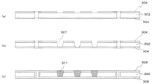
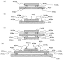
第一の実施の形態
図10(b)は、本実施形態に係る4層ISB構造を備える素子搭載基板400を示す断面図である。
First Embodiment FIG. 10B is a cross-sectional view showing an
本実施形態に係る素子搭載基板400は、基材302の上面に、絶縁樹脂膜312、フォトソルダーレジスト層328を順に積層してなる構造を有する。また、基材302の下面に、絶縁樹脂膜312、フォトソルダーレジスト層328を順に積層してなる構造を有する。
The
ここで、4層ISB構造とは、内部に配線層を4層有する構造のことであり、その配線層は絶縁樹脂膜312内およびフォトソルダーレジスト層328内に埋設されている。また、フォトソルダーレジスト層328は、その層内にビアホールを形成するプロセスの都合上、感光性を有することが求められる。
Here, the four-layer ISB structure is a structure having four wiring layers inside, and the wiring layers are embedded in the insulating
また、4層ISB構造において、基材302を挟んで、上面の絶縁樹脂膜312と下面の絶縁樹脂膜312とを構成する材料として同じ材料を用いることができ、また、上面のフォトソルダーレジスト層328と下面のフォトソルダーレジスト層328とを構成する材料として同じ材料を用いることができるので、製造工程を簡略化することができるというプロセス上の利点がある。
In the four-layer ISB structure, the same material can be used as the material constituting the insulating
また、これらの基材302、絶縁樹脂膜312、フォトソルダーレジスト層328を貫通する貫通孔327が設けられている。
In addition, a through
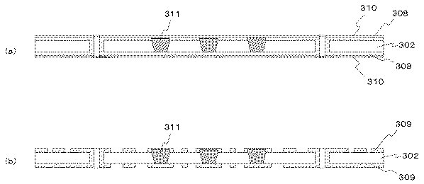
また、基材302には、銅膜308からなる配線の一部、銅膜320からなる配線の一部、ビア311の一部などが埋め込まれている。絶縁樹脂膜312には、銅膜308からなる配線の一部、銅膜320からなる配線の一部、配線309、ビア311の一部、ビア323の一部などが埋め込まれている。フォトソルダーレジスト層328には、銅膜320からなる配線の一部、ビア323の一部などが埋め込まれている。また、フォトソルダーレジスト層328には、開口部326が設けられている。
Further, a part of the wiring made of the
ここで、基材302に用いる材料としては、特にガラスエポキシ基板に限定されず、適度な剛性を有する材料であれば使用可能である。例えば、基材302として、樹脂基板やセラミック基板などを用いることができる。より具体的には、低誘電率であるため高周波特性に優れた基材を用いることができる。すなわち、ポリフェニールエチレン(PPE)、ビスマレイドトリアジン(BT−resin)、ポリテトラフルオロエチレン(テフロン(登録商標))、ポリイミド、液晶ポリマー(LCP)、ポリノルボルネン(PNB)、エポキシ系樹脂、アクリル系樹脂、セラミックあるいはセラミックと有機基材の混合体などを用いることができる。また、基材302の厚さは、たとえば、60μm程度とする。
Here, the material used for the
絶縁樹脂膜312に用いる材料としては、加熱により軟化する樹脂材料であり、絶縁樹脂膜312をある程度薄膜化させることができる樹脂材料が用いられる。特に、低誘電率であり、高周波特性に優れた樹脂材料を好適に用い得る。また、絶縁樹脂膜312の厚さは、たとえば、40μm程度とする。
The material used for the insulating
ここで、絶縁樹脂膜312には、フィラーまたは繊維等の充填材を含めることができる。フィラーとしては、たとえば粒子状または繊維状のSiO2やSiNを用いることができる。
Here, the insulating
また、フォトソルダーレジスト層328には、後述するカルド型ポリマー含有樹脂膜が用いられる。ここで、フォトソルダーレジスト層328の厚さは、たとえば30μm程度以下が好ましく、25μm程度がより好ましく用いられる。
For the photo solder resist
ここで、カルド型ポリマーは、嵩高い置換基が主鎖の運動を阻害することにより、優れた機械的強度、耐熱性および低い線膨張率を有する。よって、フォトソルダーレジスト層328にカルド型ポリマー含有樹脂膜を用いることにより、ヒートサイクルにおいて、フォトソルダーレジスト層328とその周囲の層との密着性の低下または層間剥離などが抑制される。このため、本実施形態に係る素子搭載基板400の信頼性が良好となる。
Here, the cardo type polymer has excellent mechanical strength, heat resistance, and a low linear expansion coefficient due to the bulky substituents inhibiting the movement of the main chain. Therefore, by using a cardo type polymer-containing resin film for the photo solder resist
また、上記の銅膜308からなる配線、銅膜320からなる配線、配線309、ビア311、ビア323などからなる多層配線構造としては、例えば銅配線などに限定されず、アルミニウム配線、アルミニウム合金配線、銅合金配線、ワイヤーボンディングされた金配線、金合金配線、またはこれらの混合配線などを用いることもできる。
The multilayer wiring structure including the wiring made of the
また、上記の4層ISB構造の表面または内部には、トランジスタやダイオードなどの能動素子、キャパシタや抵抗などの受動素子が設けられていてもよい。これらの能動素子または受動素子は、4層ISB中の多層配線構造に接続し、ビア323などを通じて外部の導電部材と接続可能としてもよい。 Further, an active element such as a transistor or a diode, or a passive element such as a capacitor or a resistor may be provided on the surface or inside of the four-layer ISB structure. These active elements or passive elements may be connected to a multilayer wiring structure in the four-layer ISB and connectable to an external conductive member through a via 323 or the like.
図3から図10は、本実施形態に係る素子搭載基板400の工程断面図である。
3 to 10 are process cross-sectional views of the
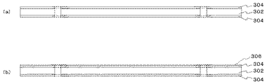
まず、図3(a)に示すように、ドリルで直径150nm程度の孔を開口した銅箔304が圧着された基材302を用意する。ここで、基材302の厚さは、たとえば、60μm程度とし、銅箔304の厚さは、たとえば、10μmから15μm程度とする。ここで、基材302に用いる材料としては、特にガラスエポキシ基板に限定されず、適度な剛性を有する材料であれば使用可能である。例えば、基材302として、樹脂基板やセラミック基板などを用いることができる。より具体的には、低誘電率であるため高周波特性に優れた基材を用いることができる。すなわち、ポリフェニールエチレン(PPE)、ビスマレイドトリアジン(BT−resin)、ポリテトラフルオロエチレン(テフロン(登録商標))、ポリイミド、液晶ポリマー(LCP)、ポリノルボルネン(PNB)、エポキシ系樹脂、アクリル系樹脂、セラミックあるいはセラミックと有機基材の混合体などを用いることができる。
First, as shown in FIG. 3A, a
図3(b)に示すように、銅箔304の上面に、フォトエッチングレジスト層306をラミネートする。
As shown in FIG. 3B, a photoetching resist layer 306 is laminated on the upper surface of the
ついで、ガラスをマスクとして露光することでフォトエッチングレジスト層306をパターニングする。その後、図4(a)および(b)に示すように、フォトエッチングレジスト層306をマスクとして、たとえば、薬液による化学エッチング加工によって、直径100nm程度のビアホール307を形成する。その後、ビアホール307内をウェット処理により粗化および洗浄する。つづいて、図4(c)に示すように、高アスペクト比対応の無電解めっき、次いで電解めっきにより、ビアホール307内を導電性材料で埋め込み、ビア311を形成した後に、全面に銅膜308を形成する。
Next, the photo-etching resist layer 306 is patterned by exposing with glass as a mask. Thereafter, as shown in FIGS. 4A and 4B, a via
ビア311は、たとえば以下のようにして形成することができる。まず、無電解銅めっきにより全面に0.5〜1μm程度の薄膜を形成した後、電解めっきにより約20μm程度の膜を形成する。無電解めっき用触媒は、通常パラジウムを用いることが多く、可とう性の絶縁樹脂に無電解用めっき用触媒を付着させるには、パラジウムを錯体の状態で水溶液に含ませ、可とう性の絶縁基材を浸漬して表面にパラジウム錯体を付着させ、そのまま、還元剤を用いて、金属パラジウムに還元することによって可とう性の絶縁基材表面にめっきを開始するための核を形成することができる。 The via 311 can be formed as follows, for example. First, after forming a thin film of about 0.5 to 1 μm on the entire surface by electroless copper plating, a film of about 20 μm is formed by electrolytic plating. The electroless plating catalyst is usually palladium, and in order to attach the electroless plating catalyst to a flexible insulating resin, palladium is included in an aqueous solution in a complex state, and the flexible insulating resin is used. It is possible to form a nucleus for initiating plating on the surface of a flexible insulating base material by dipping the base material to attach a palladium complex to the surface and reducing it to metallic palladium directly using a reducing agent. it can.
図5(a)に示すように、銅膜308の上下の表面にフォトエッチングレジスト層310をラミネートする。つづいて、図5(b)に示すように、ガラスをマスクとして露光することでパターニングした後、フォトエッチングレジスト層310をマスクとして銅めっき層308をエッチングすることにより、銅からなる配線309を形成する。たとえば、レジストから露出した箇所に、化学エッチング液をスプレー噴霧して不要な銅めっきをエッチング除去し、配線パターンを形成することができる。
As shown in FIG. 5A, a photoetching resist
次に、図6(a)に示すように、銅箔314付きの絶縁樹脂膜312を、配線309の上下から圧着する。ここで、絶縁樹脂膜312の厚さは、たとえば、40μm程度とし、銅箔314の厚さは、たとえば、10μm〜15μm程度とする。
Next, as shown in FIG. 6A, the insulating
絶縁樹脂膜312に用いる材料としては、加熱することにより軟化する材料であればどのようなものを用いることもできるが、たとえばエポキシ樹脂、BTレジン等のメラミン誘導体、液晶ポリマー、PPE樹脂、ポリイミド樹脂、フッ素樹脂、フェノール樹脂、ポリアミドビスマレイミド等を用いることができる。ここで、絶縁樹脂膜312には、フィラーまたは繊維等の充填材を含めることができる。フィラーとしては、たとえば粒子状または繊維状のSiO2やSiNを用いることができる。
As the material used for the insulating
圧着の方法としては、銅箔付き絶縁樹脂膜312を基材302および配線309に当接し、絶縁樹脂膜312内に基材302および配線309を嵌入する。次に、図6(b)に示すように、絶縁樹脂膜312を真空下または減圧下で加熱して基材302および配線309に圧着する。つづいて、図6(c)に示すように、銅箔314にX線を照射することで、銅箔314、絶縁樹脂膜312、配線309、基材302を貫通する孔315を開口する。
As a pressing method, the insulating
図7(a)に示すように、銅箔314の上下の表面にフォトエッチングレジスト層316をラミネートする。つづいて、図7(b)に示すように、ガラスをマスクとして露光することでパターニングした後、フォトエッチングレジスト層316をマスクとして、銅箔314をエッチングすることにより、銅からなる配線319を形成する。たとえば、レジストから露出した箇所に、化学エッチング液をスプレー噴霧して不要な銅箔をエッチング除去し、配線パターンを形成することができる。
As shown in FIG. 7A, a photoetching resist
図8(a)に示すように、配線319の上下の表面にフォトエッチングレジスト層317をラミネートする。つづいて、図8(b)に示すように、ガラスをマスクとして露光することでパターニングした後、フォトエッチングレジスト層317をマスクとして、たとえば、薬液による化学エッチングにより、直径100nm程度のビアホール322を形成する。その後、ビアホール322内をウェット処理により粗化および洗浄する。つづいて、図8(c)に示すように、高アスペクト比対応の無電解めっき、次いで電界めっきにより、ビアホール322内を導電性材料で埋め込み、ビア323を形成した後に、全面に銅膜320を形成する。
As shown in FIG. 8A, a photoetching resist
ビア323は、たとえば以下のようにして形成することができる。まず、無電解銅めっきにより全面に0.5〜1μm程度の薄膜を形成した後、電解めっきにより約20μm程度の膜を形成する。無電解めっき用触媒は、通常パラジウムを用いることが多く、可とう性の絶縁樹脂に無電解用めっき用触媒を付着させるには、パラジウムを錯体の状態で水溶液に含ませ、可とう性の絶縁基材を浸漬して表面にパラジウム錯体を付着させ、そのまま、還元剤を用いて、金属パラジウムに還元することによって可とう性の絶縁基材表面にめっきを開始するための核を形成することができる。 The via 323 can be formed as follows, for example. First, after forming a thin film of about 0.5 to 1 μm on the entire surface by electroless copper plating, a film of about 20 μm is formed by electrolytic plating. The electroless plating catalyst is usually palladium, and in order to attach the electroless plating catalyst to a flexible insulating resin, palladium is included in an aqueous solution in a complex state, and the flexible insulating resin is used. It is possible to form a nucleus for initiating plating on the surface of a flexible insulating base material by dipping the base material to attach a palladium complex to the surface and reducing it to metallic palladium directly using a reducing agent. it can.
図9(a)に示すように、銅膜320の上下の表面に、フォトエッチングレジスト層316をラミネートする。つづいて、図9(b)に示すように、ガラスをマスクとして露光することでパターニングした後、フォトエッチングレジスト層316をマスクとして、銅膜320をエッチングすることにより、銅からなる配線324を形成する。たとえば、レジストから露出した箇所に、化学エッチング液をスプレー噴霧して不要な銅箔をエッチング除去し、配線パターンを形成することができる。
As shown in FIG. 9A, a photoetching resist
図10(a)に示すように、配線324の上下の表面に、フォトソルダーレジスト層328をラミネートする。ここで、フォトソルダーレジスト層328の厚さは、たとえば30μm程度以下が好ましく、25μm程度がより好ましく用いられる。ラミネートの条件としては、たとえば、温度110℃、時間1〜2分、2気圧などが用いられる。その後、アフターベーク工程によりフォトソルダーレジスト層328を一部硬化させる。
As shown in FIG. 10A, a photo solder resist
フォトソルダーレジスト層328には、後述する、カルド型ポリマー含有樹脂膜が用いられる。
For the photo solder resist
つづいて、図10(b)に示すように、ガラスをマスクとして露光することでパターニングした後、フォトソルダーレジスト層328をマスクとして、たとえば、薬液による化学エッチング加工によって、ビアホール322に形成されたビア323を露出するように、たとえば、直径100nm程度のビアホール326を形成する。その後、露出されたビア323に金メッキを施す(不図示)。
Subsequently, as shown in FIG. 10B, after patterning by exposing glass as a mask, vias formed in the via holes 322 by, for example, chemical etching using a chemical solution using the photo solder resist
以下、本実施形態において、カルド型ポリマー含有樹脂膜を、フォトソルダーレジスト層328に用いることの効果について説明する。
Hereinafter, in this embodiment, the effect of using the cardo type polymer-containing resin film for the photo solder resist
ここで、カルド型ポリマーとは、式(I)に示すように、環状の基がポリマー主鎖に直接結合した構造を有するポリマーの総称である。なお、式(I)において、R1、R2はアルキレン基や芳香環を含む2価の基などの2価の基を表す。 Here, the cardo type polymer is a general term for polymers having a structure in which a cyclic group is directly bonded to a polymer main chain, as shown in the formula (I). In the formula (I), R 1 and R 2 represent a divalent group such as an alkylene group or a divalent group containing an aromatic ring.
すなわち、このカルド型ポリマーとは、四級炭素を有する嵩高い置換基が、主鎖に対して、ほぼ直角に存在する構造を有しているポリマーのことである。 That is, the cardo type polymer is a polymer having a structure in which a bulky substituent having a quaternary carbon is present substantially perpendicular to the main chain.
ここで、環状部は、飽和結合でも不飽和結合を含んでいてもよく、炭素の他、窒素原子、酸素原子、硫黄原子、リン原子等の原子を含んでいてもよい。また、環状部は多環であってもよく、縮合環であってもよい。また、環状部は、他の炭素鎖と結合していても、更には、架橋していてもよい。 Here, the cyclic portion may include a saturated bond or an unsaturated bond, and may include atoms such as a nitrogen atom, an oxygen atom, a sulfur atom, and a phosphorus atom in addition to carbon. The cyclic part may be a polycycle or a condensed ring. Moreover, even if the cyclic part is couple | bonded with the other carbon chain, it may be bridge | crosslinked further.
なお、嵩高い置換基としては、たとえば、式(I)に示すように、五員環の両側に六員環が結合し、五員環の残り一つの炭素原子が主鎖と結合した構造を有する縮合環を有するフルオレニル基などの環状の基が挙げられる。 As the bulky substituent, for example, as shown in the formula (I), a structure in which a six-membered ring is bonded to both sides of the five-membered ring and the remaining one carbon atom of the five-membered ring is bonded to the main chain. And cyclic groups such as a fluorenyl group having a condensed ring.
フルオレニル基とは、式(II)に示すように、フルオレンの9位の炭素原子が脱水素化された基であり、カルド型ポリマーにおいては、式(I)に示すように、脱水素化された炭素原子の位置で、主鎖であるアルキル基の炭素原子と結合している。 The fluorenyl group is a group in which the carbon atom at the 9-position of fluorene is dehydrogenated as shown in the formula (II). In the cardo type polymer, it is dehydrogenated as shown in the formula (I). It is bonded to the carbon atom of the alkyl group which is the main chain at the position of the carbon atom.
カルド型ポリマーは、上記構造を有するポリマーであるため、
(1)ポリマー主鎖の回転拘束
(2)主鎖及び側鎖のコンフォメーション規制
(3)分子間パッキングの阻害
(4)側鎖の芳香族置換基導入等による芳香族性の増加
といった効果を奏する。
Since the cardo type polymer is a polymer having the above structure,
(1) Rotation constraint of polymer main chain (2) Conformation regulation of main chain and side chain (3) Inhibition of intermolecular packing (4) Effect of increasing aromaticity by introduction of aromatic substituent on side chain Play.
したがって、カルド型ポリマーは、高い機械的強度、高耐熱性、溶剤溶解性、高透明性、高屈折率、低複屈折率、更には、より高い気体透過性といった特徴を有する。 Accordingly, the cardo type polymer has characteristics such as high mechanical strength, high heat resistance, solvent solubility, high transparency, high refractive index, low birefringence, and higher gas permeability.
ここで、フォトソルダーレジスト層328に用いるカルド型ポリマー含有樹脂膜は、所定の添加剤を用いて、ボイドや凹凸などの発生が抑制された状態で薄膜に成形可能である。このため、フォトソルダーレジスト層328に、25μm程度の厚さのフィルムを用いることができ、フォトソルダーレジスト層328に通常用いられている樹脂材料の厚さである35μm程度と比較すると、約2/3の厚さとなる。したがって、フォトソルダーレジスト層328にカルド型ポリマー含有樹脂膜を用いることにより、本実施形態における素子搭載基板400を小型化することができる。また、上記カルド型ポリマー含有樹脂膜をフォトソルダーレジスト層328に用いることにより、フォトソルダーレジスト層328に25μm程度の厚さのフィルムを用いることができるので、絶縁樹脂膜312の厚さである約40μmよりも、フォトソルダーレジスト層328の厚さを薄くすることができる。
Here, the cardo type polymer-containing resin film used for the photo solder resist
また、カルド型ポリマー含有樹脂膜は後述するように優れた耐湿性と密着性を有する。このため、フォトソルダーレジスト層328に、カルド型ポリマー含有樹脂膜を用いることにより、素子搭載基板400の表面に搭載される素子や他の層との密着性を向上させることができる。
The cardo type polymer-containing resin film has excellent moisture resistance and adhesion as described later. For this reason, by using a cardo type polymer-containing resin film for the photo solder resist
また、カルド型ポリマー含有樹脂膜は後述するように、優れた解像度を有する。また、本実施形態において用いられるフィルムの厚さは、フォトソルダーレジスト層に通常用いられている厚さの約2/3であるから、カルド型ポリマー含有樹脂膜を用いたフォトソルダーレジスト層328は、より優れた解像度を有する。このため、ビアホール326を形成する際の寸法精度を向上させることができる。したがって、素子搭載基板400の信頼性を向上させることができる。
Further, the cardo type polymer-containing resin film has an excellent resolution as will be described later. Moreover, since the thickness of the film used in this embodiment is about 2/3 of the thickness usually used for the photo solder resist layer, the photo solder resist
また、カルド型ポリマー含有樹脂膜は後述するように、優れた誘電特性を有する。このため、フォトソルダーレジスト層328に、カルド型ポリマー含有樹脂膜を用いることにより、フォトソルダーレジスト層328内に埋設された配線間の寄生容量が低減される。したがって、素子搭載基板400の信頼性を向上させることができる。
The cardo type polymer-containing resin film has excellent dielectric properties as will be described later. Therefore, by using a cardo type polymer-containing resin film for the photo solder resist
また、カルド型ポリマー含有樹脂膜は高い機械的強度を有することにより、フォトソルダーレジスト層328の厚さを従来の約2/3の厚さとしても、機械的強度を保つことができる。そのため、素子搭載基板400の基板全体の反りを抑制させることができる。したがって、素子搭載基板400上に搭載される素子のボンディングの精度を向上させることができる。
Further, since the cardo type polymer-containing resin film has high mechanical strength, even if the thickness of the photo solder resist
また、フォトソルダーレジスト層の形成に通常用いられるスピンコート法においては、フォトソルダーレジスト層の外周部にボイドが生じやすいという点で改善の余地を有していた。また、ポッティング法では、接着前の状態が液体であり、塗布した後にボイドが生じやすいという点で改善の余地を有していた。これに対して、本実施形態におけるフォトソルダーレジスト層328は、フィルムを圧着する際に、ボイドや凹凸などの発生が抑制されるので、フィルムが圧着された素子搭載基板400のフォトソルダーレジスト層328にもボイドや凹凸は少ない。したがって、素子搭載基板400の信頼性および製造安定性を向上させることができる。
Further, the spin coating method usually used for forming the photo solder resist layer has room for improvement in that voids are likely to be generated in the outer peripheral portion of the photo solder resist layer. Further, the potting method has room for improvement in that the state before bonding is liquid and voids are likely to occur after coating. On the other hand, the photo solder resist
なお、上記カルド型ポリマーは、カルボン酸基とアクリレート基とを同一分子鎖内に有するポリマーが架橋してなるポリマーであってもよい。従来の一般的な感光性ワニスとしては、現像性を持つカルボン酸基オリゴマーと多官能アクリルとのブレンドが用いられているが、解像度の面でさらなる改善の余地があった。一般的な感光ワニスの代わりに、カルボン酸基とアクリレート基とを同一分子鎖内に有するポリマーが架橋してなるカルド型ポリマーを用いると、現像性を持つカルボン酸と架橋基であるアクリレート基とを同一分子鎖中に有し、主鎖に嵩高い置換基を持ちラジカル拡散し難いため、カルド型ポリマー含有樹脂膜の解像度が向上する利点がある。 The cardo type polymer may be a polymer obtained by crosslinking a polymer having a carboxylic acid group and an acrylate group in the same molecular chain. As a conventional general photosensitive varnish, a blend of a carboxylic acid group oligomer having developability and a polyfunctional acrylic is used, but there is room for further improvement in terms of resolution. In place of a general photosensitive varnish, if a cardo type polymer obtained by crosslinking a polymer having a carboxylic acid group and an acrylate group in the same molecular chain is used, a developable carboxylic acid and an acrylate group which is a crosslinking group In the same molecular chain and has a bulky substituent in the main chain and is difficult to radically diffuse. Therefore, there is an advantage that the resolution of the cardo type polymer-containing resin film is improved.
また、カルド型ポリマー含有樹脂膜は、以下に示す諸物性値を満たすことが望ましい。なお、以下の諸物性値は、フィラーなどを含まない樹脂部分についての値であり、フィラーなどを添加することにより、適宜調整可能である。 Moreover, it is desirable that the cardo type polymer-containing resin film satisfy the following physical property values. In addition, the following various physical property values are values for a resin portion that does not contain a filler or the like, and can be appropriately adjusted by adding a filler or the like.
ここで、上記カルド型ポリマー含有樹脂膜のガラス転移温度(Tg)は、例えば180℃以上とすることができ、特に好ましくは190℃以上である。ガラス転移温度がこの範囲にあると、カルド型ポリマー含有樹脂膜の耐熱性が向上する。 Here, the glass transition temperature (Tg) of the cardo polymer-containing resin film can be, for example, 180 ° C. or higher, and particularly preferably 190 ° C. or higher. When the glass transition temperature is in this range, the heat resistance of the cardo type polymer-containing resin film is improved.
また、上記カルド型ポリマー含有樹脂膜のガラス転移温度(Tg)は、例えば220℃以下とすることができ、特に好ましくは210℃以下である。ガラス転移温度がこの範囲のカルド型ポリマー含有樹脂膜であれば、通常の製法により安定的に製造可能である。ガラス転移温度は、例えばバルク試料の動的粘弾性測定(DMA)により測定可能である。 Moreover, the glass transition temperature (Tg) of the said cardo type polymer containing resin film can be made into 220 degrees C or less, for example, Most preferably, it is 210 degrees C or less. A cardo type polymer-containing resin film having a glass transition temperature in this range can be stably produced by a normal production method. The glass transition temperature can be measured, for example, by dynamic viscoelasticity measurement (DMA) of a bulk sample.
また、上記カルド型ポリマー含有樹脂膜のTg以下の領域における線膨張係数(CTE)は、例えば80ppm/℃以下とすることができ、特に好ましくは75ppm/℃以下である。線膨張係数がこの範囲にあると、カルド型ポリマー含有樹脂膜と、他の部材などとの密着性が向上する。 Moreover, the linear expansion coefficient (CTE) in the area | region below Tg of the said cardo type polymer containing resin film can be 80 ppm / degrees C or less, for example, Most preferably, it is 75 ppm / degrees C or less. When the linear expansion coefficient is in this range, the adhesion between the cardo type polymer-containing resin film and other members is improved.
また、上記カルド型ポリマー含有樹脂膜のTg以下の領域における線膨張係数(CTE)は、例えば50ppm/℃以上とすることができ、特に好ましくは55ppm/℃以上である。また、上記カルド型ポリマー含有樹脂膜にフィラーを配合することにより、CTEを20ppm/℃以下の樹脂組成物を得ることもできる。線膨張係数がこの範囲のカルド型ポリマー含有樹脂膜であれば、通常の製法により安定的に製造可能である。線膨張係数は、例えば熱機械分析装置(TMA)による熱膨張測定により測定可能である。 Moreover, the linear expansion coefficient (CTE) in the area | region below Tg of the said cardo type polymer containing resin film can be 50 ppm / degrees C or more, for example, Most preferably, it is 55 ppm / degrees C or more. In addition, a resin composition having a CTE of 20 ppm / ° C. or less can be obtained by blending a filler with the cardo polymer-containing resin film. If the cardo type polymer-containing resin film has a linear expansion coefficient in this range, it can be stably produced by an ordinary production method. The linear expansion coefficient can be measured, for example, by measuring thermal expansion using a thermomechanical analyzer (TMA).
また、上記カルド型ポリマー含有樹脂膜の熱伝導率は、例えば0.50W/cm2・sec以下とすることができ、特に好ましくは0.35W/cm2・sec以下である。熱伝導率がこの範囲にあると、カルド型ポリマー含有樹脂膜の耐熱性が向上する。 The thermal conductivity of the cardo polymer-containing resin film can be, for example, 0.50 W / cm 2 · sec or less, and particularly preferably 0.35 W / cm 2 · sec or less. When the thermal conductivity is within this range, the heat resistance of the cardo type polymer-containing resin film is improved.
また、上記カルド型ポリマー含有樹脂膜の熱伝導率は、例えば0.10W/cm2・sec以上とすることができ、特に好ましくは0.25W/cm2・sec以上である。熱伝導率がこの範囲のカルド型ポリマー含有樹脂膜であれば、通常の製法により安定的に製造可能である。熱伝導率は、例えば円板熱流計法(ASTM E1530)により測定可能である。 The thermal conductivity of the cardo type polymer containing resin film, for example, 0.10 W / cm may be a 2 · sec or more, and particularly preferably 0.25W / cm 2 · sec or more. A cardo type polymer-containing resin film having a thermal conductivity in this range can be stably produced by a normal production method. The thermal conductivity can be measured, for example, by a disk heat flow meter method (ASTM E1530).
また、上記カルド型ポリマー含有樹脂膜の10〜100μm直径のビアにおけるビアアスペクト比は、例えば0.5以上とすることができ、特に好ましくは1以上である。ビアアスペクト比がこの範囲にあると、カルド型ポリマー含有樹脂膜の解像度が向上する。 In addition, the via aspect ratio of the 10 to 100 μm diameter via of the cardo polymer-containing resin film can be set to 0.5 or more, and particularly preferably 1 or more. When the via aspect ratio is within this range, the resolution of the cardo type polymer-containing resin film is improved.
また、上記カルド型ポリマー含有樹脂膜の10〜100μm直径のビアにおけるビアアスペクト比は、例えば5以下とすることができ、特に好ましくは2以下である。ビアアスペクト比がこの範囲のカルド型ポリマー含有樹脂膜であれば、通常の製法により安定的に製造可能である。 The via aspect ratio of the cardo polymer-containing resin film in a via having a diameter of 10 to 100 μm can be, for example, 5 or less, particularly preferably 2 or less. If the cardo type polymer-containing resin film has a via aspect ratio in this range, it can be stably produced by an ordinary production method.
また、上記カルド型ポリマー含有樹脂膜の周波数1MHzの交流電界を印加した場合の誘電率は、例えば4以下とすることができ、特に好ましくは3以下である。誘電率がこの範囲にあると、カルド型ポリマー含有樹脂膜の高周波特性をはじめとする誘電特性が向上する。 Moreover, the dielectric constant at the time of applying the alternating electric field of frequency 1MHz of the said cardo type polymer containing resin film can be 4 or less, for example, Especially preferably, it is 3 or less. When the dielectric constant is within this range, the dielectric properties including the high frequency properties of the cardo type polymer-containing resin film are improved.
また、上記カルド型ポリマー含有樹脂膜の周波数1MHzの交流電界を印加した場合の誘電率は、例えば0.1以上とすることができ、特に好ましくは2.7以上である。誘電率がこの範囲のカルド型ポリマー含有樹脂膜であれば、通常の製法により安定的に製造可能である。 The dielectric constant of the cardo polymer-containing resin film when an AC electric field having a frequency of 1 MHz is applied can be, for example, 0.1 or more, and particularly preferably 2.7 or more. A cardo type polymer-containing resin film having a dielectric constant in this range can be stably produced by an ordinary production method.
また、上記カルド型ポリマー含有樹脂膜の周波数1MHzの交流電界を印加した場合の誘電正接は、例えば0.04以下とすることができ、特に好ましくは0.029以下である。誘電正接がこの範囲にあると、カルド型ポリマー含有樹脂膜の高周波特性をはじめとする誘電特性が向上する。 The dielectric loss tangent of the cardo polymer-containing resin film when an AC electric field having a frequency of 1 MHz is applied can be, for example, 0.04 or less, and particularly preferably 0.029 or less. When the dielectric loss tangent is within this range, the dielectric properties including the high frequency properties of the cardo type polymer-containing resin film are improved.
また、上記カルド型ポリマー含有樹脂膜の周波数1MHzの交流電界を印加した場合の誘電正接は、例えば0.001以上とすることができ、特に好ましくは0.027以上である。誘電正接がこの範囲のカルド型ポリマー含有樹脂膜であれば、通常の製法により安定的に製造可能である。 The dielectric loss tangent of the cardo polymer-containing resin film when an AC electric field having a frequency of 1 MHz is applied can be, for example, 0.001 or more, and particularly preferably 0.027 or more. If the dielectric loss tangent is a cardo type polymer-containing resin film in this range, it can be stably produced by an ordinary production method.
また、上記カルド型ポリマー含有樹脂膜の24時間吸水率(wt%)は、例えば3wt%以下とすることができ、特に好ましくは1.5wt%以下である。24時間吸水率(wt%)がこの範囲にあると、カルド型ポリマー含有樹脂膜の耐湿性を向上することができる。 Further, the 24-hour water absorption (wt%) of the cardo type polymer-containing resin film can be, for example, 3 wt% or less, and particularly preferably 1.5 wt% or less. When the water absorption rate (wt%) for 24 hours is in this range, the moisture resistance of the cardo type polymer-containing resin film can be improved.
また、上記カルド型ポリマー含有樹脂膜の24時間吸水率(wt%)は、例えば0.5wt%以上とすることができ、特に好ましくは1.3wt%以上である。24時間吸水率(wt%)がこの範囲のカルド型ポリマー含有樹脂膜であれば、通常の製法により安定的に製造可能である。 In addition, the 24-hour water absorption (wt%) of the cardo type polymer-containing resin film can be, for example, 0.5 wt% or more, and particularly preferably 1.3 wt% or more. If the 24-hour water absorption (wt%) is within this range, the cardo type polymer-containing resin film can be stably produced by an ordinary production method.
これら上記の複数の特性をカルド型ポリマー含有樹脂膜が満たす場合には、カルド型ポリマー含有樹脂膜を用いるフォトソルダーレジスト層328に要求される、薄膜化、機械的強度、耐熱性、他の部材との密着性、解像度、誘電特性、耐湿性などの諸特性がバランス良く実現される。
When the cardo type polymer-containing resin film satisfies the above-mentioned plurality of characteristics, thinning, mechanical strength, heat resistance, other members required for the photo solder resist
第二の実施形態
図11は、本実施の形態における4層ISB構造を備える素子搭載基板400への半導体素子の各種搭載方法を模式的に示した断面図である。
Second Embodiment FIG. 11 is a cross-sectional view schematically showing various mounting methods of semiconductor elements on an
本実施形態において、カルド型ポリマー含有樹脂膜とは、第一の実施形態で記載したカルド型ポリマー含有樹脂膜と同じである。 In this embodiment, the cardo polymer-containing resin film is the same as the cardo polymer-containing resin film described in the first embodiment.
第一の実施形態で説明した素子搭載基板400に半導体素子を搭載してなる半導体装置には、多くの形式がある。例えば、フリップチップ接続やワイヤーボンディングにより接続して搭載する形式がある。また、素子搭載基板400に半導体素子をフェイスアップ構造やフェイスダウン構造により搭載する形式がある。また、素子搭載基板400の片面や両面に半導体素子を搭載する形式がある。さらには、これらの各種形式を組み合わせてなる形式もある。
There are many types of semiconductor devices in which semiconductor elements are mounted on the
具体的には、例えば図11(a)に示すように、第一の実施形態の素子搭載基板400の上部にLSIなどの半導体素子500をフリップチップ形式で搭載し得る。このとき、素子搭載基板400上面の電極パッド402a、402bと、半導体素子500の電極パッド502a、502bとがそれぞれ互いに直接接続する。
Specifically, for example, as shown in FIG. 11A, a
また、図11(b)に示すように、素子搭載基板400の上部にLSIなどの半導体素子500をフェイスアップ構造で搭載し得る。このとき、素子搭載基板400上面の電極パッド402a、402bは、半導体素子500上面の電極パッド502a、502bと、それぞれ金線504a、504bによりワイヤーボンディング接続されている。
Further, as shown in FIG. 11B, a
また、図11(c)に示すように、素子搭載基板400の上部にLSIなどの半導体素子500をフリップチップ形式で搭載し、素子搭載基板400の下部にICなどの半導体素子600をフリップチップ形式で搭載し得る。このとき、素子搭載基板400上面の電極パッド402a、402bは、半導体素子500の電極パッド502a、502bとそれぞれ互いに直接接続する。また、素子搭載基板400下面の電極パッド404a、404bは、半導体素子600の電極パッド602a、602bとそれぞれ互いに直接接続する。
Further, as shown in FIG. 11C, a
また、図11(d)に示すように、素子搭載基板400の上部にLSIなどの半導体素子500をフェイスアップ構造で搭載し、素子搭載基板400を、プリント基板700の上部に搭載し得る。このとき、素子搭載基板400上面の電極パッド402a、402bは、半導体素子500上面の電極パッド502a、502bと、それぞれ金線504a、504bによりワイヤーボンディング接続される。また、素子搭載基板400下面の電極パッド404a、404bは、プリント基板700上面の電極パッド702a、702bとそれぞれ互いに直接接続する。
Further, as shown in FIG. 11D, a
上記いずれの構造からなる半導体装置においても、第一の実施形態で説明したように、素子搭載基板400を構成するフォトソルダーレジスト層328に、カルド型ポリマー含有樹脂膜を用いた素子搭載基板400を用いている。ここで、カルド型ポリマー含有樹脂膜は、上述するように、耐湿性、密着性、誘電特性、解像度などの諸特性に優れている。そのため、素子搭載基板400上に搭載される素子や、フォトソルダーレジスト層328と接する絶縁樹脂膜312との密着性に優れ、フォトソルダーレジスト層328上にビアホールなどを形成する際の寸法精度を向上させることができ、かつ、寄生容量を低減させることができる。また、フォトソルダーレジスト層328に、薄膜化しても機械的強度の高いフィルムを用いている。そのため、素子搭載基板400における基板全体の反りを抑制することができる。したがって、素子搭載基板400上に素子を搭載する際の精度を向上させることができる。この結果、素子搭載基板400上に素子を搭載することで、信頼性が高く、小型化された半導体装置を提供することができる。
In the semiconductor device having any of the above structures, as described in the first embodiment, the
以上、発明の好適な実施の形態を説明した。しかし、本発明は上述の実施の形態に限定されず、当業者が本発明の範囲内で上述の実施の形態を変形可能なことはもちろんである。 The preferred embodiments of the invention have been described above. However, the present invention is not limited to the above-described embodiments, and it goes without saying that those skilled in the art can modify the above-described embodiments within the scope of the present invention.
たとえば、フォトソルダーレジスト層328に加えて、基材302または絶縁樹脂膜312に、カルド型ポリマー含有樹脂膜を用いてもよい。
For example, a cardo type polymer-containing resin film may be used for the
フォトソルダーレジスト層328に加えて、基材302に、カルド型ポリマー含有樹脂膜を用いることにより、以下の効果を得ることができる。
By using a cardo type polymer-containing resin film for the
基材302に用いるカルド型ポリマー含有樹脂膜は、所定の添加剤を用いて、ボイドや凹凸などの発生が抑制された状態で薄膜に成形可能である。このため、基材302に、40μm程度の厚さのフィルムを用いることができ、基材に通常用いられている樹脂材料の厚さである60μm程度と比較すると、約2/3の厚さとなる。また、カルド型ポリマー含有樹脂膜は、上述するように優れた密着性および耐熱性を有する。したがって、カルド型ポリマー含有樹脂膜を、フォトソルダーレジスト層328に加えて、基材302にも用いることにより、本実施形態における素子搭載基板400の信頼性をより向上させつつ、一層小型化することができる。また、上記素子搭載基板400上に半導体素子を搭載することにより、信頼性がより向上され、一層小型化された半導体装置を提供することができる。
The cardo type polymer-containing resin film used for the
フォトソルダーレジスト層328に加えて、絶縁樹脂膜312に、カルド型ポリマー含有樹脂膜を用いることにより、以下の効果を得ることができる。
By using a cardo type polymer-containing resin film for the insulating
絶縁樹脂膜312に用いるカルド型ポリマー含有樹脂膜は、所定の添加剤を用いて、ボイドや凹凸などの発生が抑制された状態で薄膜に成形可能である。このため、絶縁樹脂膜312に、25μm程度の厚さのフィルムを用いることができ、絶縁樹脂膜に通常用いられている樹脂材料の厚さである40μm程度と比較すると、約2/3の厚さとなる。したがって、カルド型ポリマー含有樹脂膜を、フォトソルダーレジスト層328に加えて、絶縁樹脂膜312にも用いることにより、素子搭載基板400を一層小型化することができる。また、カルド型ポリマー含有樹脂膜は、上述するように優れた密着性、耐熱性および誘電特性などを有するので、絶縁樹脂膜312の層間密着性が向上され、寄生容量が低減される。このため、素子搭載基板400の信頼性を向上させることができる。さらに、フィルムを圧着する際に、ボイドや凹凸の発生が抑制されるので、フィルムが圧着された素子搭載基板400の絶縁樹脂膜312にもボイドや凹凸は少ない。したがって、カルド型ポリマー含有樹脂膜を、フォトソルダーレジスト層328に加えて、絶縁樹脂膜312にも用いることにより、本実施形態における素子搭載基板400の信頼性をより向上させつつ、一層小型化することができる。また、上記素子搭載基板400上に半導体素子を搭載することにより、信頼性と製造安定性が顕著に向上され、一層小型化された半導体装置を提供することができる。
The cardo-type polymer-containing resin film used for the insulating
また、フォトソルダーレジスト層328に加えて、基材302および絶縁樹脂膜312に、カルド型ポリマー含有樹脂膜を用いてもよい。
In addition to the photo solder resist
ここで、カルド型ポリマー含有樹脂膜は上述するように、耐熱性、機械的強度、密着性、耐湿性、誘電特性、解像度特性などの諸特性に優れ、かつ、薄膜に成形可能であるため、基材302、絶縁樹脂膜312およびフォトソルダーレジスト層328は、剛性、耐熱性、層間密着性、寄生容量、素子搭載時の寸法精度、平坦性などの諸特性に優れている。このため、フォトソルダーレジスト層328に加えて、基板302、絶縁樹脂膜312のすべてに、カルド型ポリマー含有樹脂膜を用いることにより、素子搭載基板400の信頼性と製造安定性をより顕著に向上させることができ、より一層の小型化を図ることができる。また、上記素子搭載基板400上に半導体素子を搭載することにより、信頼性と製造安定性がより顕著に向上され、より一層小型化された半導体装置を提供することができる。
Here, as described above, the cardo type polymer-containing resin film is excellent in various properties such as heat resistance, mechanical strength, adhesion, moisture resistance, dielectric properties, resolution properties, and can be molded into a thin film. The
また、上記実施形態においては、4層ISB構造を備える素子搭載基板400を構成するフォトソルダーレジスト層328に、カルド型ポリマー含有樹脂膜を用いる構成としたが、たとえば、配線層を4層以上、たとえば6層の配線層を有するISB構造を備える素子搭載基板のフォトソルダーレジスト層にカルド型ポリマー含有樹脂膜を用いてもよいし、他の半導体パッケージのフォトソルダーレジスト層にカルド型ポリマー含有樹脂膜を用いてもよい。
Moreover, in the said embodiment, although it was set as the structure which uses a cardo type | mold polymer containing resin film for the photo solder resist
302 基材、304 銅箔、306 フォトエッチングレジスト層、307 ビアホール、308 銅膜、309 配線、310 フォトエッチングレジスト層、311 ビア、312 絶縁樹脂膜、314 銅箔、315 孔、316 フォトエッチングレジスト層、317 フォトエッチングレジスト層、319 配線、320 銅膜、322 ビアホール、323 ビア、324 配線、326 ビアホール、327 貫通孔、328 フォトソルダーレジスト層、400 素子搭載基板、402 電極パッド、404 電極パッド、500 半導体素子、502 電極パッド、504 金線、600 半導体素子、602 電極パッド、700 プリント基板、702 電極パッド。
302 substrate, 304 copper foil, 306 photo-etching resist layer, 307 via hole, 308 copper film, 309 wiring, 310 photo-etching resist layer, 311 via, 312 insulating resin film, 314 copper foil, 315 hole, 316 photo-etching resist
Claims (5)
基材と、該基材上に設けられた絶縁膜と、該絶縁膜上に設けられたソルダーレジスト層とを含み、
前記ソルダーレジスト層は、カルド型ポリマーを含むことを特徴とする素子搭載基板。 An element mounting board for mounting elements,
A base material, an insulating film provided on the base material, and a solder resist layer provided on the insulating film,
The element mounting substrate, wherein the solder resist layer contains a cardo type polymer.
前記ソルダーレジスト層に前記素子を接続する配線が設けられていることを特徴とする素子搭載基板。 In the element mounting substrate according to claim 1,
An element mounting substrate, wherein wiring for connecting the element is provided in the solder resist layer.
前記ソルダーレジスト層のガラス転移温度が180℃以上220℃以下であり、
前記ソルダーレジスト層の周波数1MHzの交流電界を印加した場合の誘電正接が0.001以上0.04以下であることを特徴とする素子搭載基板。 In the element mounting substrate according to claim 1 or 2,
The glass transition temperature of the solder resist layer is 180 ° C. or higher and 220 ° C. or lower,
An element mounting substrate, wherein a dielectric loss tangent of 0.001 or more and 0.04 or less when an alternating electric field having a frequency of 1 MHz is applied to the solder resist layer.
前記ソルダーレジスト層のガラス転移温度以下の領域における線膨張係数が50ppm/℃以上80ppm/℃以下であることを特徴とする素子搭載基板。 In the element mounting substrate according to claim 3,
The element mounting board | substrate characterized by the linear expansion coefficient in the area | region below the glass transition temperature of the said soldering resist layer being 50 ppm / degrees C or more and 80 ppm / degrees C or less.
該素子搭載基板に搭載されている半導体素子と、
を備えることを特徴とする半導体装置。 The element mounting substrate according to any one of claims 1 to 4,
A semiconductor element mounted on the element mounting substrate;
A semiconductor device comprising:
Priority Applications (4)
| Application Number | Priority Date | Filing Date | Title |
|---|---|---|---|
| JP2004105764A JP2005294441A (en) | 2004-03-31 | 2004-03-31 | Element mounting board and semiconductor device employing it |
| TW94107788A TWI255535B (en) | 2004-03-31 | 2005-03-15 | Device mounting board and semiconductor apparatus using the same |
| US11/086,640 US20050238878A1 (en) | 2004-03-31 | 2005-03-22 | Device mounting board |
| CNB2005100628153A CN100429767C (en) | 2004-03-31 | 2005-03-31 | Device mounting board |
Applications Claiming Priority (1)
| Application Number | Priority Date | Filing Date | Title |
|---|---|---|---|
| JP2004105764A JP2005294441A (en) | 2004-03-31 | 2004-03-31 | Element mounting board and semiconductor device employing it |
Publications (1)
| Publication Number | Publication Date |
|---|---|
| JP2005294441A true JP2005294441A (en) | 2005-10-20 |
Family
ID=35327056
Family Applications (1)
| Application Number | Title | Priority Date | Filing Date |
|---|---|---|---|
| JP2004105764A Pending JP2005294441A (en) | 2004-03-31 | 2004-03-31 | Element mounting board and semiconductor device employing it |
Country Status (1)
| Country | Link |
|---|---|
| JP (1) | JP2005294441A (en) |
Cited By (1)
| Publication number | Priority date | Publication date | Assignee | Title |
|---|---|---|---|---|
| JP2007227420A (en) * | 2006-02-21 | 2007-09-06 | Nippon Steel Chem Co Ltd | Multilayer printed wiring board |
-
2004
- 2004-03-31 JP JP2004105764A patent/JP2005294441A/en active Pending
Cited By (2)
| Publication number | Priority date | Publication date | Assignee | Title |
|---|---|---|---|---|
| JP2007227420A (en) * | 2006-02-21 | 2007-09-06 | Nippon Steel Chem Co Ltd | Multilayer printed wiring board |
| JP4587974B2 (en) * | 2006-02-21 | 2010-11-24 | 新日鐵化学株式会社 | Manufacturing method of multilayer printed wiring board |
Similar Documents
| Publication | Publication Date | Title |
|---|---|---|
| CN100429768C (en) | Vice mounting board and semiconductor apparatus using device mounting board | |
| JP3877717B2 (en) | Semiconductor device and manufacturing method thereof | |
| JP4434845B2 (en) | Semiconductor module, method for manufacturing the same, and semiconductor device | |
| US20110011829A1 (en) | Device Mounting Board | |
| US7198986B2 (en) | Electronic parts built-in substrate and method of manufacturing the same | |
| KR20050020739A (en) | Multilayer wiring circuit module and method for fabricating the same | |
| TWI242855B (en) | Chip package structure, package substrate and manufacturing method thereof | |
| JP4338570B2 (en) | Element mounting substrate and semiconductor device using the same | |
| US20050238878A1 (en) | Device mounting board | |
| TWI631684B (en) | Medium substrate and the manufacture thereof | |
| US8039948B2 (en) | Device mounting board and semiconductor apparatus using the same | |
| JP2005294285A (en) | Semiconductor module and its manufacturing method | |
| JP2005294352A (en) | Element mounting board and semiconductor device employing it | |
| JP2005294441A (en) | Element mounting board and semiconductor device employing it | |
| JP2004200668A (en) | Semiconductor device, method of manufacturing the same, and sheet-like wiring member | |
| JP2005294465A (en) | Element mounting board and semiconductor device employing it | |
| JP2005268669A (en) | Manufacturing method of semiconductor device | |
| JP2005294414A (en) | Element mounting board, its manufacturing method and semiconductor device employing it | |
| JP4413206B2 (en) | Semiconductor device and manufacturing method thereof | |
| JP2005109068A (en) | Semiconductor device and manufacturing method thereof | |
| KR101563163B1 (en) | Embedded substrate and method for manufacturing the same | |
| JPH0878566A (en) | Resin sealed semiconductor device and manufacturing method thereof | |
| TW202335197A (en) | Electronic package and manufacturing method thereof | |
| JP2005286146A (en) | Semiconductor device and manufacturing method thereof | |
| JP2004027186A (en) | Embedding resin composition and wiring board using the same |
Legal Events
| Date | Code | Title | Description |
|---|---|---|---|
| A621 | Written request for application examination |
Free format text: JAPANESE INTERMEDIATE CODE: A621 Effective date: 20061023 |
|
| A977 | Report on retrieval |
Free format text: JAPANESE INTERMEDIATE CODE: A971007 Effective date: 20080409 |
|
| A131 | Notification of reasons for refusal |
Free format text: JAPANESE INTERMEDIATE CODE: A131 Effective date: 20080415 |
|
| A521 | Written amendment |
Free format text: JAPANESE INTERMEDIATE CODE: A523 Effective date: 20080616 |
|
| A02 | Decision of refusal |
Free format text: JAPANESE INTERMEDIATE CODE: A02 Effective date: 20090602 |