JP2005294426A - Electrochemical device and electronic device using the same - Google Patents
Electrochemical device and electronic device using the same Download PDFInfo
- Publication number
- JP2005294426A JP2005294426A JP2004105444A JP2004105444A JP2005294426A JP 2005294426 A JP2005294426 A JP 2005294426A JP 2004105444 A JP2004105444 A JP 2004105444A JP 2004105444 A JP2004105444 A JP 2004105444A JP 2005294426 A JP2005294426 A JP 2005294426A
- Authority
- JP
- Japan
- Prior art keywords
- exterior body
- electronic device
- conductive exterior
- lead terminal
- electrochemical element
- Prior art date
- Legal status (The legal status is an assumption and is not a legal conclusion. Google has not performed a legal analysis and makes no representation as to the accuracy of the status listed.)
- Pending
Links
Images

Landscapes
- Electric Double-Layer Capacitors Or The Like (AREA)
Abstract
Description
本発明は、電気化学素子及びこれを用いた電子装置に関する。 The present invention relates to an electrochemical element and an electronic device using the same.
ハードディスク装置等の電子装置においては一般に、装置の停止により主電源からの電力の供給が断たれる場合でも、磁気ヘッドをディスクから離れた位置にあるランプに退避させたり、ディスク上のデータの記録を行わないシッピングゾーンあるいはCSS(Contact Start Stop)領域へ退避(リトラクト)させたりする必要がある。 In an electronic device such as a hard disk device, in general, even when the power supply from the main power supply is cut off due to the stop of the device, the magnetic head is retracted to a lamp located away from the disk, or data on the disk is recorded. It is necessary to retreat (retract) to a shipping zone or CSS (Contact Start Stop) area where no operation is performed.
このため、ハードディスク装置等の電子装置においては通常、補助電源が内蔵されており、かかる補助電源としては、従来、例えば電気二重層キャパシタを備えたものが知られている(例えば特許文献1参照)。ここで、電気二重層キャパシタにおいては一般的に、外装ケースとしてニッケル等の導電性部材が使用されている。
しかしながら、上述した電気二重層キャパシタは以下の示す課題を有していた。 However, the electric double layer capacitor described above has the following problems.
即ち上記電気二重層キャパシタは、電気二重層キャパシタを内蔵するハードディスク装置の製造途中において、電気二重層キャパシタをハードディスク装置に設置する際に、作業者が静電気を帯びていると、その静電気が電気二重層キャパシタを通じて磁気ヘッドに伝わるおそれがある。ここで、磁気ヘッドの読出し部は、GMR(Giant Magneto-Resistance)素子を備えているが、このGMR素子は、極めて薄い膜を積層してなる薄膜積層部である。このため、静電気が読出し部に急激に伝わると、その読出し機能に悪影響を与えるおそれがあり、最悪の場合読み出し部分を破壊してしまうおそれがある。上記の問題は、ハードディスク装置に限らず、PCカード、ICカード等、薄膜積層部を有する電子装置の製造途中においても生じる可能性がある。 That is, when the electric double layer capacitor is installed in the hard disk device in the course of manufacturing the hard disk device incorporating the electric double layer capacitor, if the operator is charged with static electricity, the static electricity is There is a risk of being transmitted to the magnetic head through the multilayer capacitor. Here, the reading unit of the magnetic head includes a GMR (Giant Magneto-Resistance) element, and this GMR element is a thin film laminated part formed by laminating extremely thin films. For this reason, when static electricity is rapidly transmitted to the reading unit, the reading function may be adversely affected. In the worst case, the reading unit may be destroyed. The above problem is not limited to a hard disk device, and may occur during the manufacture of an electronic device having a thin film stacking unit, such as a PC card or an IC card.
本発明は、上記事情に鑑みてなされたものであり、電子装置における薄膜積層部への悪影響を十分に防止できる電気化学素子及びこれを用いた電子装置を提供することを目的とする。 This invention is made | formed in view of the said situation, and it aims at providing the electrochemical element which can fully prevent the bad influence to the thin film laminated part in an electronic device, and an electronic apparatus using the same.
本発明者らは、上記課題を解決するため鋭意検討した結果、以下の発明により、上記課題を解決しうることを見出し、本発明を完成するに至った。 As a result of intensive studies to solve the above problems, the present inventors have found that the above problems can be solved by the following invention, and have completed the present invention.
即ち本発明は、第1リード端子部を有する第1の導電性外装体と、前記第1の導電性外装体に対向して配置され、第2リード端子部を有する第2の導電性外装体と、前記第1の導電性外装体と前記第2の導電性外装体とによって挟まれる被挟持部と、前記第1の導電性外装体及び前記第2の導電性外装体を被覆する最外層とを備えており、前記被挟持部が、一対の電極と、前記一対の電極の間に設けられる電解質とを備えており、前記第1リード端子部の少なくとも一部、及び前記第2リード端子部の少なくとも一部が露出しており、前記最外層が1.0×10⁴Ωcm以上1.0×10¹²Ωcm以下の比抵抗を有する高抵抗材料で構成されていることを特徴とする電気化学素子である。 That is, the present invention provides a first conductive exterior body having a first lead terminal portion, and a second conductive exterior body disposed opposite to the first conductive exterior body and having a second lead terminal portion. A sandwiched portion sandwiched between the first conductive exterior body and the second conductive exterior body, and an outermost layer covering the first conductive exterior body and the second conductive exterior body And the sandwiched portion includes a pair of electrodes and an electrolyte provided between the pair of electrodes, and at least a part of the first lead terminal portion and the second lead terminal. At least part of the portion is exposed, and the outermost layer is made of a high resistance material having a specific resistance of 1.0 × 10 4 Ωcm or more and 1.0 × 10 12 Ωcm or less. It is a chemical element.
この電気化学素子によれば、電気化学素子及び薄膜積層部を有する電子装置の製造過程において以下の利点が得られる。即ち、薄膜積層部を設置した後に、静電気を帯びた作業者が、電子装置に当該電気化学素子を取り付ける場合でも、作業者から第1の導電性外装体及び第2の導電性外装体を通って、薄膜積層部へ電流が急激に流れることを十分に防止することが可能となる。 According to this electrochemical element, the following advantages can be obtained in the manufacturing process of the electronic device having the electrochemical element and the thin film laminated portion. That is, after the thin film stacking unit is installed, even if an electrostatically charged worker attaches the electrochemical element to the electronic device, the worker passes through the first conductive exterior body and the second conductive exterior body. Thus, it is possible to sufficiently prevent a current from flowing rapidly to the thin film laminated portion.
上記電気化学素子においては、被挟持部が一対の電極間にセパレータを更に備えてもよい。 In the electrochemical device, the sandwiched portion may further include a separator between the pair of electrodes.
上記最外層は、前記第1の導電性外装体と、前記第2の導電性外装体と、前記被挟持部とを備える電気化学素体を、前記第1リード端子部の少なくとも一部及び前記第2リード端子部の少なくとも一部が露出されるように、1.0×10⁴Ωcm以上1.0×10¹²Ωcm以下の比抵抗を有する高抵抗材料を含む塗料中に浸漬して乾燥することにより得られるものであることが好ましい。 The outermost layer includes an electrochemical element including the first conductive exterior body, the second conductive exterior body, and the sandwiched portion, at least a part of the first lead terminal portion, and the It is dipped in a paint containing a high resistance material having a specific resistance of 1.0 × 10 4 Ωcm or more and 1.0 × 10 12 Ωcm or less and dried so that at least a part of the second lead terminal portion is exposed. It is preferable that it is obtained by this.
この電気化学素子によれば、上記最外層が上記電気化学素体を上記塗料中に浸漬し乾燥してなるため、第1の導電性外装体及び第2の導電性外装体のそれぞれが、1.0×10⁴Ωcm以上1.0×10¹²Ωcm以下の比抵抗を有する高抵抗材料で十分に被覆されることになる。即ち第1の導電性外装体及び第2の導電性外装体が露出されることが十分に防止される。このため、静電気を帯びた作業者が、薄膜積層部を有する電子装置に当該電気化学素子を取り付ける場合でも、作業者から薄膜積層部への電流の急激な流れをより十分に防止することが可能となる。また、最外層が上記電気化学素体を上記塗料中に浸漬し乾燥してなるため、第1の導電性外装体及び第2の導電性外装体とこれらを被覆する最外層との間で隙間の形成が十分に防止され、隙間に起因する電荷のチャージが十分に防止される。このため、チャージした電荷による薄膜積層部への電流の急激な流れも十分に防止される。 According to this electrochemical element, since the outermost layer is formed by immersing the electrochemical element body in the paint and drying, each of the first conductive exterior body and the second conductive exterior body is 1 It is sufficiently covered with a high resistance material having a specific resistance of 0.0 × 10 4 Ωcm or more and 1.0 × 10 12 Ωcm or less. That is, it is possible to sufficiently prevent the first conductive exterior body and the second conductive exterior body from being exposed. For this reason, even when an electrostatically charged worker attaches the electrochemical element to an electronic device having a thin film stacking section, it is possible to more sufficiently prevent a rapid flow of current from the worker to the thin film stacking section. It becomes. In addition, since the outermost layer is formed by immersing the electrochemical element in the paint and drying, there is a gap between the first conductive outer body and the second conductive outer body and the outermost layer covering them. Formation is sufficiently prevented, and charge due to the gap is sufficiently prevented. For this reason, the rapid flow of the electric current to the thin film laminated part by the charged electric charge is fully prevented.
上記電気化学素子においては、最外層がシート状となっており、接着剤層を介して前記第1の導電性外装体及び前記第2の導電性外装体のそれぞれを被覆していることが好ましい。この場合、接着剤層によって最外層が第1の導電性外装体及び第2の導電性外装体のそれぞれに密着しているため、最外層と第1の導電性外装体及び第2の導電性外装体との間で隙間の形成が十分に防止され、隙間に起因する電荷のチャージが十分に防止される。このため、チャージした電荷による薄膜積層部への電流の急激な流れも十分に防止される。 In the said electrochemical element, it is preferable that the outermost layer is a sheet form and coat | covers each of the said 1st electroconductive exterior body and the said 2nd electroconductive exterior body via the adhesive bond layer. . In this case, since the outermost layer is in close contact with each of the first conductive outer package and the second conductive outer package by the adhesive layer, the outermost layer, the first conductive outer package, and the second conductive A gap is sufficiently prevented from being formed between the outer package and the charge due to the gap is sufficiently prevented. For this reason, the rapid flow of the electric current to the thin film laminated part by the charged electric charge is fully prevented.
上記電気化学素子において、1.0×10⁴Ωcm以上1.0×10¹²Ωcm以下の比抵抗を有する高抵抗材料とは、例えば、アルミナ、マグネシア、シリカ、チタニア、ジルコニアなどの無機酸化物、炭化ケイ素、炭化チタンなどの無機炭化物、窒化タンタル、窒化ニオブ、窒化バナジウムなどの無機窒化物からなる群より選ばれる1種を含むものである。 In the electrochemical device, the high resistance material having a specific resistance of 1.0 × 10 4 Ωcm or more and 1.0 × 10 12 Ωcm or less is, for example, an inorganic oxide such as alumina, magnesia, silica, titania, zirconia, It includes one selected from the group consisting of inorganic carbides such as silicon carbide and titanium carbide, and inorganic nitrides such as tantalum nitride, niobium nitride, and vanadium nitride.
高抵抗材料の比抵抗が1.0×10⁴Ωcm以上1.0×10¹⁰Ωcm以下であると、より好ましい。また、高抵抗材料の比抵抗が1.0×10⁴Ωcm以上1.0×10⁶Ωcm以下であると、さらに好ましい。このような高抵抗材料としては、例えば、マグネシア、シリカ、チタニア、ジルコニア、炭化ケイ素、炭化チタン、窒化タンタル、窒化ニオブ、窒化バナジウムなどを用いることができる。高抵抗材料の比抵抗が1.0×10⁴Ωcm以下の場合、電気化学素子表面からの電荷の移動が急激に生じ、周囲の電子部品を破壊してしまう傾向がある。また、高抵抗材料の比抵抗が1.0×10¹⁰Ωcm以上であると、電気化学素子の表面にチャージがより溜まり易くなる傾向がある。 The specific resistance of the high resistance material is more preferably 1.0 × 10 4 Ωcm or more and 1.0 × 10 10 Ωcm or less. The specific resistance of the high resistance material is more preferably 1.0 × 10 4 Ωcm or more and 1.0 × 10 6 Ωcm or less. As such a high resistance material, for example, magnesia, silica, titania, zirconia, silicon carbide, titanium carbide, tantalum nitride, niobium nitride, vanadium nitride, or the like can be used. When the specific resistance of the high resistance material is 1.0 × 10 4 Ωcm or less, the movement of electric charges from the surface of the electrochemical element is abruptly generated and the surrounding electronic components tend to be destroyed. Further, when the specific resistance of the high resistance material is 1.0 × 10 10 Ωcm or more, the charge tends to be more easily accumulated on the surface of the electrochemical element.
ポリイミド及びポリアミドは、水分阻止能が高いため電子部品の外装部品材料として広く用いられている。しかし、一般にポリイミド及びポリアミドは、1017Ωcm〜1022Ωcmの高い比抵抗を有するため、チャージアップを生じやすい傾向にある。この場合、汎用のポリイミド又はポリアミドのシートを導電性の接着剤によって第1及び第2導電性外装体の表面に接着して用いることができる。この場合の接着剤は、1.0×10⁴Ωcm以上1.0×10¹⁰Ωcm以下の比抵抗を有する接着剤を選択して用いることができる。つまり、この発明において、最外層は1.0×10⁴Ωcm以上1.0×10¹⁰Ωcm以下の比抵抗を有する接着剤と、ポリイミド及びポリアミド又はこれらのいずれか一方からなる層とを含んで構成されている。例えば、グラファイト、アルミニウム、錫などのフィラーを分散させた接着剤を用いるのが好ましい。これにより、ポリイミド及びポリアミドの水分阻止能を維持しつつ、導電性の外装体を得ることができる。 Polyimides and polyamides are widely used as exterior component materials for electronic components because of their high moisture blocking ability. However, since polyimide and polyamide generally have a high specific resistance of 10 17 Ωcm to 10 22 Ωcm, they tend to be charged up easily. In this case, a general-purpose polyimide or polyamide sheet can be used by adhering to the surfaces of the first and second conductive exterior bodies with a conductive adhesive. In this case, an adhesive having a specific resistance of 1.0 × 10 4 Ωcm or more and 1.0 × 10 10 Ωcm or less can be selected and used. That is, in this invention, the outermost layer includes an adhesive having a specific resistance of 1.0 × 10 4 Ωcm or more and 1.0 × 10 10 Ωcm or less, and a layer made of polyimide and polyamide or one of these. It is configured. For example, it is preferable to use an adhesive in which fillers such as graphite, aluminum, and tin are dispersed. Thereby, an electroconductive exterior body can be obtained, maintaining the water blocking ability of polyimide and polyamide.
さらに、ポリイミド及びポリアミドに帯電防止処理を行ったものは、本発明に用いる最外層として好適に用いることができる。帯電防止処理としては、電子線などのエネルギー照射によって表面の一部をグラファイト化する方法を用いることができる。あるいは、高分子骨格中にスルホン酸基やスルフィン酸基を導入した構造としてもよい。これにより、ポリイミド及びポリアミドが帯電防止構造を有するものとなる。これらの方法によっても、ポリイミド及びポリアミドの水分阻止能を維持しつつ、導電性の外装体を得ることができる。このような帯電防止処理されたポリイミド及びポリアミドは、シート状に加工して接着して用いても良い。特にスルホン酸基やスルフィン酸基を導入したポリイミド及びポリアミドは、適当な溶媒に分散させて塗布しても良い。分散溶媒としては、水、アルコール、ジメチルホルムアミドなどの極性溶媒を用いることが好ましい。 Further, those obtained by subjecting polyimide and polyamide to antistatic treatment can be suitably used as the outermost layer used in the present invention. As the antistatic treatment, a method of graphitizing a part of the surface by irradiation with energy such as an electron beam can be used. Alternatively, a structure in which a sulfonic acid group or a sulfinic acid group is introduced into the polymer skeleton may be used. Thereby, polyimide and polyamide have an antistatic structure. Also by these methods, it is possible to obtain a conductive exterior body while maintaining the water blocking ability of polyimide and polyamide. Such antistatic treated polyimide and polyamide may be processed into a sheet and bonded. In particular, polyimides and polyamides into which sulfonic acid groups or sulfinic acid groups are introduced may be dispersed in an appropriate solvent and applied. As the dispersion solvent, it is preferable to use a polar solvent such as water, alcohol or dimethylformamide.
上記電気化学素子は、前記高抵抗材料が、アルミナ、マグネシア、シリカ、チタニア、炭化ケイ素、炭化チタン、窒化タンタル、窒化ニオブ、窒化バナジウム及びジルコニアからなる群より選ばれる少なくとも1種を含み、前記最外層が薄膜であることが好ましい。 In the electrochemical device, the high-resistance material includes at least one selected from the group consisting of alumina, magnesia, silica, titania, silicon carbide, titanium carbide, tantalum nitride, niobium nitride, vanadium nitride, and zirconia, The outer layer is preferably a thin film.
この場合、最外層が薄膜でない場合に比べて、軽量・省スペース化のニーズに対応できるという利点がある。 In this case, there is an advantage that the needs for light weight and space saving can be met as compared with the case where the outermost layer is not a thin film.
本発明において、「薄膜」とは、常温大気圧の環境下において、自立が困難なもの(基体の補助無くして形状を維持できないもの)を言う。本発明の薄膜は、2μm〜100μmの膜厚範囲であることが好ましい。また、前記高抵抗材料の膜厚は2μm〜70μmであることがより好ましい。加えて、前記高抵抗材料の膜厚は2μm〜50μmであることがさらに好ましい。膜厚が2μm未満の場合、実際の抵抗値が膜全体あるいは部分的に高くなってしまうため、電荷のチャージが生じやすくなる傾向にある。また、膜厚が100μmを越えた場合、薄膜に蓄積される内部応力(全応力)が大きくなるため、薄膜の破壊や剥離が生じやすくなる傾向にある。内部応力(全応力)は膜厚の増加と共に大きくなっていくが、本発明の場合、膜厚が100μm以下であれば実用上問題のない範囲である。 In the present invention, the term “thin film” refers to a film that is difficult to stand independently in a room temperature and atmospheric pressure environment (that cannot maintain its shape without the assistance of a substrate). The thin film of the present invention preferably has a film thickness range of 2 μm to 100 μm. The film thickness of the high resistance material is more preferably 2 μm to 70 μm. In addition, the thickness of the high resistance material is more preferably 2 μm to 50 μm. When the film thickness is less than 2 μm, the actual resistance value becomes high as a whole or a part of the film, so that charge tends to be easily generated. Further, when the film thickness exceeds 100 μm, the internal stress (total stress) accumulated in the thin film becomes large, and therefore the thin film tends to be broken or peeled off. The internal stress (total stress) increases as the film thickness increases, but in the case of the present invention, if the film thickness is 100 μm or less, it is in a range where there is no practical problem.
また本発明は、上述した電気化学素子と、電気化学素子を収容する収容部及び薄膜積層部を有する電子装置本体部とを備えており、収容部には、電気化学素子を構成する第1リード端子部及び第2リード端子部と接触される接続端子が設けられており、収容部が、前記電子装置本体部の表面側に設けられており、電気化学素子が収容部に対して着脱可能に収容されていることを特徴とする電子装置である。 In addition, the present invention includes the above-described electrochemical element, and an electronic device main body having an accommodating part for accommodating the electrochemical element and a thin film stacking part, and the accommodating part includes a first lead constituting the electrochemical element. A connection terminal to be in contact with the terminal portion and the second lead terminal portion is provided, and the accommodating portion is provided on the surface side of the electronic device main body, so that the electrochemical element can be attached to and detached from the accommodating portion. The electronic device is housed.
この電子装置によれば、静電気を帯びた作業者が電子装置本体部の収容部から電気化学素子を電子装置本体部の外側に取り外す場合でも、作業者から薄膜積層部への電流の流れが十分に防止される。 According to this electronic device, even when an electrostatically charged worker removes the electrochemical element from the housing of the electronic device main body to the outside of the electronic device main body, sufficient current flows from the worker to the thin film stacking portion. To be prevented.
上記電子装置においては、電気化学素子が電気二重層キャパシタであることが好ましい。この場合、電気化学素子として、電気二重層キャパシタ以外のものを用いる場合と比較して、瞬時に充放電が可能で、かつ、高エネルギー密度が得られるという利点がある。 In the electronic device, the electrochemical element is preferably an electric double layer capacitor. In this case, as compared with the case where an electrochemical element other than the electric double layer capacitor is used, there are advantages that charging and discharging can be performed instantaneously and a high energy density can be obtained.
上記電子装置においては、例えば前記電子装置本体部が、少なくとも1枚の磁気ディスクと、前記磁気ディスクに記録された磁気情報を読み出す読出し部を有する磁気ヘッドとを備えており、前記読出し部が、前記薄膜積層部を有するものである。 In the electronic device, for example, the electronic device main body includes at least one magnetic disk and a magnetic head having a reading unit that reads magnetic information recorded on the magnetic disk, and the reading unit includes: It has the thin film lamination part.
なお、本発明の電子装置において、薄膜積層部とは、薄膜の積層体であって、電子装置の機能を果たすために必要不可欠なものであり、且つ静電気により電子装置を正常に機能させられなくなる程度の耐電圧特性を有するものを言う。 In the electronic device of the present invention, the thin film stack is a thin film stack, which is indispensable for performing the function of the electronic device, and the electronic device cannot function normally due to static electricity. It has a withstand voltage characteristic.
本発明の電気化学素子によれば、薄膜積層部を有する電子装置の製造過程において、静電気を帯びた作業者から薄膜積層部への電流の急激な流れを十分に防止することが可能となる。このため、電子装置における薄膜積層部への悪影響を十分に防止でき、電子装置の製造歩留まりの低下を十分に防止することができる。 According to the electrochemical element of the present invention, it is possible to sufficiently prevent an abrupt flow of current from an electrostatically charged worker to the thin film stack in the manufacturing process of the electronic device having the thin film stack. For this reason, it is possible to sufficiently prevent an adverse effect on the thin film laminated portion in the electronic device, and it is possible to sufficiently prevent a decrease in the manufacturing yield of the electronic device.
また本発明の電子装置によれば、静電気を帯びた作業者が電子装置本体部の収容部から電気化学素子を電子装置本体部の外側に取り外す場合でも、作業者から薄膜積層部への電流の急激な流れを十分に防止することが可能となる。このため、電子装置における薄膜積層部への悪影響を十分に防止できる。 Further, according to the electronic device of the present invention, even when an electrostatically charged worker removes the electrochemical element from the housing of the electronic device main body to the outside of the electronic device main body, the electric current from the worker to the thin film stacking portion is reduced. Sudden flow can be sufficiently prevented. For this reason, the bad influence to the thin film laminated part in an electronic device can fully be prevented.
以下、本発明の実施形態について詳細に説明する。なお、全図中、同一又は同等の構成要素には同一符号を付し、重複する説明を省略する。 Hereinafter, embodiments of the present invention will be described in detail. In all the drawings, the same or equivalent components are denoted by the same reference numerals, and redundant description is omitted.
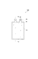
図1は、本発明に係る電気化学素子の第1実施形態を示す平面図、図2は、図1のII−II線に沿った断面図である。 FIG. 1 is a plan view showing a first embodiment of an electrochemical element according to the present invention, and FIG. 2 is a cross-sectional view taken along the line II-II in FIG.
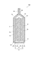
図2に示すように、電気二重層キャパシタ(電気化学素子)100は、第1の導電性外装体2と、第2の導電性外装体4とを備えており、第1の導電性外装体2と第2の導電性外装体4とは互いに対向して配置されている。
As shown in FIG. 2, the electric double layer capacitor (electrochemical element) 100 includes a first conductive
第1の導電性外装体2は、平板状の本体部2aと、第1のリード端子部2bと、本体部2a及び第1のリード端子部2bとを連結する連結部2cとで構成されており、第2の導電性外装体4も、平板状の本体部4aと、第2のリード端子部4bと、本体部4a及び第2のリード端子部4bとを連結する連結部4cとで構成されている(図1参照)。
The first conductive
第1の導電性外装体2及び第2の導電性外装体4は、導電性を有するものであれば特に限定されず、第1の導電性外装体2及び第2の導電性外装体4としては、例えばアルミニウム、ニッケル、銅等が用いられる。これらのうち、電解質溶液に対して耐食性に優れているという観点から、アルミニウムが好ましく用いられる。
The first conductive
なお、第1の導電性外装体2及び第2の導電性外装体4は同一材料であっても、異なる材料で構成されても構わない。
The first conductive
第1の導電性外装体2と第2の導電性外装体4との間には、電荷を蓄える機能を有する蓄電部(被挟持部)6が設けられており、蓄電部6は、本体部2aと本体部4aとによって挟まれている。
Between the first conductive
蓄電部6は、第1蓄電部8と第2蓄電部10とを有しており、第1蓄電部8と第2蓄電部10とは、集電体12を介して直列に接続されている。第1蓄電部8及び第2蓄電部10は、互いに対向する第1電極20及び第2電極22を備えており、第1電極20と第2電極22との間にはセパレータ24が設けられている。セパレータ24は、第1電極20と第2電極22とによって挟まれている。そして、セパレータ24には電解質溶液(電解質)が含浸されている。これにより、第1電極20と第2電極22との間に電解液が設けられることになる。
The
第1電極20及び第2電極22は、例えば、活物質とフッ素ゴムとの混合物で構成される。活物質には、例えば、アセチレンブラック、グラファイト、黒鉛、活性炭などを選択して、あるいは、これらのうちのいずれかを混合して用いることができる。セパレータ24は、絶縁性の多孔体で構成されている。絶縁性の多孔体としては、例えばセルロース不織布が挙げられる。電解質溶液には、水系電解液と有機系電解液とがあるが、有機系電解液が好ましい。このような有機系電解液としては、例えばトリエチルメチルアンモニウムフルオロボーレート(TEMABF4)からなる溶質をプロピレンカーボネート(PC)からなる溶媒に混合させたものが挙げられる。溶質としては、上記のほか、Et4NBF4、Et4NPF6、Et4PBF4、Et3MeNBF4が挙げられ、溶媒としては、上記のほか、ガンマブチロラクトン(GBL)、エチレンカーボネート(EC)、スルフォラン(SFL)等が挙げられる。
The
そして、第1蓄電部8の周縁部及び第2蓄電部10の周縁部は、封止材14によって封止されている。これにより、第1蓄電部8及び第2蓄電部10中の電解液への水分の浸入が防止され、耐電圧の低下が十分に防止される。封止材14は、外部からの水分の浸入を防止できるものであればよく、封止材14としては、例えばポリプロピレン系材料が用いられる。こうして電気化学素体16が構成されている。
The peripheral edge of the first
この電気化学素体16の表面は最外層18で被覆されており、最外層18には、第1開口部26が形成され、これにより第1リード端子部2bの一部が露出している。また図1に示すように、最外層18には、第2開口部28が形成され、これにより、第2リード端子部4bの一部が露出している。このように第1リード端子部2b及び第2リード端子部4bを露出させるのは、第1リード端子部2b及び第2リード端子部4bと、電気二重層キャパシタ100が設置されるべき電子装置本体部側の接続端子との接触を可能とするためである。
The surface of the
ここで、最外層18は、上記電気化学素体16を、第1リード端子部2bの一部及び第2リード端子部4bの一部が露出されるように、1.0×10⁴Ωcm以上1.0×10¹²Ωcm以下の比抵抗を有する高抵抗材料を含む塗料中に浸漬し乾燥することにより得られるものである。上記塗料は、上記高抵抗材料のほか、上記高抵抗材料を溶解又は分散させる溶媒を含み、かかる溶媒としては、例えばターピネオール、アセトン、アルコール、ジメチルホルムアミド、水などが用いられる。
Here, the
従って、最外層18は、1.0×10⁴Ωcm以上1.0×10¹²Ωcm以下の比抵抗を有する高抵抗材料で構成されている。
Therefore, the
上記電気二重層キャパシタ100によれば、最外層18が電気化学素体16を上記塗料中に浸漬し乾燥してなるため、第1の導電性外装体2及び第2の導電性外装体4のそれぞれが、1.0×10⁴Ωcm以上1.0×10¹²Ωcm以下の比抵抗を有する高抵抗材料で十分に覆われることになる。即ち第1の導電性外装体2及び第2の導電性外装体4が露出されることが十分に防止される。
According to the electric
このため、電気二重層キャパシタ100によれば、例えばGMR素子を有する読出し部を備えた磁気ヘッドと、電気二重層キャパシタ100の第1リード端子部2bおよび第2リード端子部4bと接触される接続端子とを有するハードディスク装置の製造過程において次のような利点が得られる。
For this reason, according to the electric
即ち、磁気ヘッド及び接続端子が設置された後に、静電気を帯びた作業者が当該電気二重層キャパシタ100を接続端子に接触させる場合でも、第1の導電性外装体2及び第2の導電性外装体4が最外層18で覆われることにより、作業者から第1の導電性外装体2及び第2の導電性外装体4への静電気の急激な流れが十分に防止される。このため、作業者から読出し部への電流の急激な流れによる読み出し部分の破壊を十分に防止することが可能となる。
In other words, even when an electrostatically charged worker makes the electric
また、最外層18が電気化学素体16を上記塗料中に浸漬し乾燥してなるため、第1の導電性外装体2及び第2の導電性外装体4と最外層18との間で隙間の形成が十分に防止され、隙間に起因する電荷のチャージが十分に防止される。このため、チャージした電荷による読出し部への電流の急激な流れも十分に防止される。
In addition, since the
以上より、電気二重層キャパシタ100によれば、ハードディスク装置における読出し部の破壊などの悪影響を十分に防止でき、ハードディスク装置の製造歩留まりの低下を十分に防止することができる。
As described above, according to the electric
上記のような高抵抗材料は、1×10⁴Ωcm以上1×10¹²Ωcm以下の比抵抗を有するものであれば特に限定されず、高抵抗材料としては、例えば、アルミナ、マグネシア、シリカ、チタニア、炭化ケイ素、炭化チタン、窒化タンタル、窒化ニオブ、窒化バナジウム、ジルコニア又はこれらの1つ以上を含むものが挙げられる。また、ポリイミド、ポリアミド又はこれらの両方を含むものであってもよい。 The high resistance material is not particularly limited as long as it has a specific resistance of 1 × 10 4 Ωcm or more and 1 × 10 12 Ωcm or less. Examples of the high resistance material include alumina, magnesia, silica, and titania. , Silicon carbide, titanium carbide, tantalum nitride, niobium nitride, vanadium nitride, zirconia, or those containing one or more thereof. Moreover, a polyimide, polyamide, or both of these may be included.
また、高抵抗材料の比抵抗は、外部(例えば、作業者の身体)の静電気の電荷を、電子部品を破壊しないよう緩やかに移動させるという理由から、1×10⁵Ωcm以上であることが好ましい。また高抵抗材料の比抵抗は、帯電を防止するという理由から、好ましくは1×10¹⁰Ωcm以下である。 In addition, the specific resistance of the high resistance material is preferably 1 × 10 5 Ωcm or more because the electrostatic charge of the outside (for example, the worker's body) is gently moved so as not to destroy the electronic component. . Further, the specific resistance of the high resistance material is preferably 1 × 10 10 Ωcm or less because it prevents charging.
次に、本発明の電気化学素子の第2実施形態について説明する。 Next, a second embodiment of the electrochemical device of the present invention will be described.
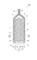
図3は、本発明に係る電気化学素子の第2実施形態を示す断面図である。図3に示すように、電気二重層キャパシタ200は、シート状の最外層18a及び18bが、接着剤層201を介して第1の導電性外装体2及び第2の導電性外装体4を被覆している点で第1実施形態の電気二重層キャパシタ100と相違する。即ち、本実施形態の電気二重層キャパシタ200は、第1の導電性外装体2及び第2の導電性外装体4の表面の大きさ及び形状に合わせて、シート状の最外層18a,18bが接着剤層201を介して第1の導電性外装体2及び第2の導電性外装体4の表面に貼り付けられている点で第1実施形態の電気二重層キャパシタ100と相違する。
FIG. 3 is a cross-sectional view showing a second embodiment of the electrochemical device according to the present invention. As shown in FIG. 3, in the electric
このようにシート状の最外層18が接着剤層201を介して第1の導電性外装体2及び第2の導電性外装体4に貼り付けられているため、接着剤層201によって最外層18が第1の導電性外装体2及び第2の導電性外装体4のそれぞれに密着している。このため、最外層18と第1の導電性外装体2及び第2の導電性外装体4との間で隙間の形成が十分に防止され、隙間に起因する電荷のチャージが十分に防止される。このため、チャージした電荷による読出し部への電流の急激な流れも十分に防止される。その結果、ハードディスク装置における読出し部の破壊などの悪影響を十分に防止でき、ハードディスク装置の製造歩留まりの低下を十分に防止することができる。
Since the sheet-like
次に、本発明に係る電子装置の第1実施形態について説明する。
Next, a first embodiment of an electronic device according to the present invention will be described.
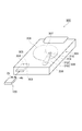
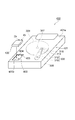
図4は本実施形態に係る電子装置としてのハードディスク装置を概略的に示す斜視図、図5は、図4の薄膜積層部を拡大して示す平面図である。なお、図4においては、ハードディスク装置から電気二重層キャパシタ100を取り外した状態が示されている。
4 is a perspective view schematically showing a hard disk device as an electronic device according to the present embodiment, and FIG. 5 is an enlarged plan view showing the thin film stacking portion of FIG. FIG. 4 shows a state where the electric
図4に示すように、ハードディスク装置300は、薄型直方体形状の本体部(電子装置本体部)301を備えており、本体部301にはケーブル接続用コネクタ302が設けられている。本体部301の表面側であって、コネクタ302と反対側の面301aには、電気二重層キャパシタ100を収容するための差込穴(収容部)303が形成されている。差込穴303には、電気二重層キャパシタ100が着脱可能に収容されるようになっている。このため、電気二重層キャパシタ100,200は、本体部301の外側に自由に取り出すことが可能であり、本体部301の外側から自由に装着することも可能である。また、電気二重層キャパシタ100が第1リード端子部2b及び第2リード端子部4b側から差込穴303に差し込まれると、第1リード端子部2b及び第2リード端子部4bが本体部301内の2つの接続端子304,305のそれぞれに接触するようになっている。
As shown in FIG. 4, the
本体部301の内部には、磁気ディスク306が、回転軸307によって回転可能に設けられており、回転軸307には、回転モータ(図示せず)により回転駆動力が付与されるようになっている。
Inside the
また本体部301の内部には回転軸308が設けられ、回転軸308は、回転モータ(図示せず)により回転可能とされている。回転軸308には、磁気ヘッド組立体309が固定されている。磁気ヘッド組立体309は、回転軸308に固定されるアーム部310と、アーム部310の先端に設けられる磁気ヘッド312とで構成されており、磁気ヘッド312は、読出し部314及び書込み部316を有している。ここで、読出し部314はGMR素子を有しており、GMR素子は、反強磁性層であるピン層315、固定磁性層であるピンド層318、非磁性層320、フリー層322を順次積層してなる積層体324を含んでいる。
A
ピン層315は、PtMn、NiO等の反強磁性体を材料とし、ピン層315の厚みは通常、3nm〜50nmである。ピンド層318は、Fe、Co、Ni、NiFe、CoFe、CoZrNb、FeCoNi等の強磁性体を材料とし、ピンド層318の厚みは通常、0.5nm〜5nmである。非磁性層320は、Cu、Ru、Rh、Ir、Au、Ag等の非磁性体を材料とし、非磁性層320の厚みは通常、1nm〜4nmである。フリー層322は、Fe、Co、Ni、NiFe、CoFe、CoZrNb、FeCoNi等の強磁性体を材料とし、フリー層322の厚みは通常、0.5nm〜10nmである。このように、積層体324は、極めて薄い膜を積層してなり、薄膜積層部を構成している。
The pinned
上記ハードディスク装置300においては、本体部301の収容穴303に電気二重層キャパシタ100が着脱可能に収容されているが、電気二重層キャパシタ100は、1.0×10⁴Ωcm以上1.0×10¹²Ωcm以下の比抵抗を有する高抵抗材料を含んで構成される最外層18を有する。特に、電気二重層キャパシタ100においては、最外層18が電気化学素体16を上記塗料中に浸漬し乾燥してなるものである。このため、第1の導電性外装体2及び第2の導電性外装体4のそれぞれが、1.0×10⁴Ωcm以上1.0×10¹²Ωcm以下の比抵抗を有する高抵抗材料で十分に被覆されることになる。即ち第1の導電性外装体2及び第2の導電性外装体4が露出されることが十分に防止される。
In the
従って、静電気を帯びた作業者が、本体部301の収容穴303から電気二重層キャパシタ100を取り外す場合でも、作業者から第1の導電性外装体2及び第2の導電性外装体4への静電気の急激な流れが十分に防止される。従って、作業者から読出し部314への電流の急激な流れも十分に防止され、その結果、作業者の静電気に起因する読出し部314の損傷が十分に防止されることになる。
Therefore, even when a worker who is charged with static electricity removes the electric
特に、最外層18が電気化学素体16を上記塗料中に浸漬し乾燥してなるため、第1の導電性外装体2及び第2の導電性外装体4と最外層18との間で隙間の形成が十分に防止され、隙間に起因する電荷のチャージが十分に防止される。このため、チャージした電荷による読出し部314への電流の急激な流れも十分に防止される。
In particular, since the
よって、ハードディスク装置300によれば、電気二重層キャパシタ100を取り外す場合でも、読出し部314への悪影響を十分に防止でき、ハードディスク装置300の損傷が十分に防止される。
Therefore, according to the
次に、本発明に係る電子装置の第2実施形態について説明する。 Next, a second embodiment of the electronic device according to the present invention will be described.
図6は、本発明の電子装置の第2実施形態を示す斜視図であり、ハードディスク装置から電気二重層キャパシタ100を取り外した状態が示されている。
FIG. 6 is a perspective view showing a second embodiment of the electronic device of the present invention, and shows a state in which the electric
図6に示すように、本実施形態のハードディスク装置400は、まず、収容部としての嵌込部403が、本体部401の表面のうち磁気ディスク306と対向する表面401a側に形成されている点でハードディスク装置300と相違する。また、嵌込部403は、電気二重層キャパシタ100が嵌め込まれる形状とされ、嵌込部403の底部403aに、電気二重層キャパシタ100の露出された第1リード端子部2b及び第2リード端子部4bと接触される接続端子404,405が設けられる点でもハードディスク装置300と相違する。
As shown in FIG. 6, in the
このハードディスク装置400によれば、ハードディスク装置300と同様に、電気二重層キャパシタ100を取り外す場合でも、読出し部314への悪影響を十分に防止でき、ハードディスク装置400の損傷が十分に防止される。
According to the
本発明は、上記実施形態に限定されるものではない。例えば上記実施形態では、電気化学素子として、電気二重層キャパシタ100,200が用いられているが、電気二重層キャパシタ100,200に代えて、1次電池やリチウムイオン電池等の2次電池が用いられても構わない。この場合、被挟持部は、蓄電部6ではなく、発電機能を有する発電部となる。但し、電気化学素子が電気二重層キャパシタである場合には、電気化学素子として電気二重層キャパシタ以外のものを用いる場合と比較して、瞬時に充放電が可能で、かつ、高エネルギーが得られるという利点がある。
The present invention is not limited to the above embodiment. For example, in the above embodiment, the electric
また、上記実施形態では、電子装置として、ハードディスク装置が用いられているが、本発明の電子装置は、ハードディスク装置に限られるものでなく、PCカード、ICカード等であってもよい。ここで、PCカード、ICカード等における薄膜積層部は、MOSにおける絶縁膜やFETゲート絶縁膜等で構成される集積回路である。この場合でも、電気化学素子を取り外す場合に、薄膜積層部への悪影響を十分に防止でき、電子装置の機能が損なわれることを十分に防止することができる。 In the above embodiment, a hard disk device is used as the electronic device. However, the electronic device of the present invention is not limited to the hard disk device, and may be a PC card, an IC card, or the like. Here, the thin film laminated portion in a PC card, an IC card or the like is an integrated circuit constituted by an insulating film in MOS, an FET gate insulating film, or the like. Even in this case, when the electrochemical element is removed, it is possible to sufficiently prevent the adverse effect on the thin film stacking portion and sufficiently prevent the function of the electronic device from being impaired.
更に、本発明の電気化学素子に係る実施形態では、最外層18が、塗料に浸漬して乾燥するか、シート状とし接着剤層を介して貼り付けることによって形成されているが、最外層18がアルミナ又はジルコニアを含む薄膜である場合には、最外層18は、気相合成によって製造することができる。この場合でも、塗料中に電気化学素体を浸漬塗布する場合と同様に、第1の導電性外装体2及び第2の導電性外装体4の露出を十分に防止することができ、静電気を帯びた作業者から、第1の導電性外装体2及び第2の導電性外装体4を経て、磁気ヘッドの読出し部等へ急激に電流が流れることを十分に防止することができる。
Furthermore, in the embodiment according to the electrochemical device of the present invention, the
ここで、気相合成は、容器内に、支持体と、アルミニウム又はジルコニウムのターゲットを配置し、容器内の真空度を例えば10〜20Paとし、アルゴンガスと酸素ガスをそれぞれ20sccm、15sccずつ真空容器内に導入しながら、支持体とターゲットとの間に、13.56HzのRF周波数の電界を印加することにより行えばよい。 Here, in the vapor phase synthesis, a support and an aluminum or zirconium target are arranged in a container, the degree of vacuum in the container is, for example, 10 to 20 Pa, and argon gas and oxygen gas are respectively 20 sccm and 15 scc in a vacuum container. It may be performed by applying an electric field having an RF frequency of 13.56 Hz between the support and the target while being introduced into the substrate.
なお、上記薄膜には、アルミナ又はジルコニアに代えて、マグネシア、シリカ、チタニア、炭化ケイ素、炭化チタン、窒化タンタル、窒化ニオブ、窒化バナジウムが含まれていてもよく、この場合でも、アルミナ又はジルコニアが含まれる場合と同様の効果が得られる。 The thin film may contain magnesia, silica, titania, silicon carbide, titanium carbide, tantalum nitride, niobium nitride, and vanadium nitride instead of alumina or zirconia. The same effect as the case where it is contained is acquired.
更に、上記実施形態の電気二重層キャパシタ100,200では、第1リード端子部2b及び第2リード端子部4bがそれぞれ本体部2a,4aの外側に設けられているが、図7に示す電気二重層キャパシタ150のように、第1リード端子部2b及び第2リード端子部4bがそれぞれ本体部2a,4aの内側に設けられてもよい。この場合、電気二重層キャパシタ150の小型化を図ることができる。なお、図7において、露出している部分が第1リード端子部2b及び第2リード端子部4bであり、この形態では、連結部2c、4cは不要である。
Furthermore, in the electric
以下、実施例及び比較例に基づいて本発明をより具体的に説明するが、本発明は以下の実施例に限定されるものではない。 EXAMPLES Hereinafter, although this invention is demonstrated more concretely based on an Example and a comparative example, this invention is not limited to a following example.
(実施例1)
以下の手順により、図2に示した電気二重層キャパシタ100と同様の構成を有する実施例1の電気二重層キャパシタを作製した。
(Example 1)
The electric double layer capacitor of Example 1 having the same configuration as that of the electric
(電気二重層キャパシタ素体の作製)
まず、電極を有する集電体を以下のようにして作製した。即ち、集電体には、アルミニウム箔(厚さ50μm)を矩形状に切断したもの(10×10mm)を採用し、これら集電体上に電極を形成した。具体的には、賦活処理した活性炭(比表面積2000m2/g、クラレケミカル製BP−20)と、バインダーとしてのフッ素ゴム(デュポン社製、Viton−GF)と、導電助剤としてのアセチレンブラック(電気化学工業製、DENKABLACK)とを、所定量のメチルイソブチルケトンにそれぞれ80重量%、10重量%、10重量%となるように混合・混練した後にペースト化し、メタルマスク法で集電体の主面(両面)の中央部(8×8mm)に塗布し、乾燥して電極とした。電極の乾燥後の厚さは50μmであった。
(Preparation of electric double layer capacitor body)
First, a current collector having an electrode was produced as follows. That is, as the current collector, an aluminum foil (thickness: 50 μm) cut into a rectangular shape (10 × 10 mm) was adopted, and electrodes were formed on these current collectors. Specifically, activated activated carbon (specific surface area 2000 m 2 / g, BP-20 manufactured by Kuraray Chemical), fluororubber (manufactured by DuPont, Viton-GF), and acetylene black (conducting aid) ( Denka Black, manufactured by Denki Kagaku Kogyo Co., Ltd.) was mixed and kneaded with a predetermined amount of methyl isobutyl ketone so as to be 80% by weight, 10% by weight, and 10% by weight, respectively. It apply | coated to the center part (8x8 mm) of the surface (both surfaces), and it dried and set it as the electrode. The thickness of the electrode after drying was 50 μm.
次に、導電性外装体を2枚作成した。2枚の導電性外装体は上記の集電体の中心軸に対し、図2のリード端子部(2b、4b)と、連結部(2c、4c)とを、中心軸から片方の側にずらした形状とした。このとき、リード端子部と連結部を除いた部分の形状は上記集電体と同一とした。 Next, two conductive exterior bodies were prepared. The two conductive armor bodies shift the lead terminal portions (2b, 4b) and the connecting portions (2c, 4c) of FIG. 2 from the central axis to one side with respect to the central axis of the current collector. Shape. At this time, the shape of the portion excluding the lead terminal portion and the connecting portion was the same as that of the current collector.
次に、上記2枚の導電性外装体に対し、上記集電体における電極の作製に用いたペーストと同じペーストを、上記導電性外装体における集電体と対応する部分(8×8mm)に塗布し、乾燥して電極を形成した。電極の乾燥後の厚さは50μmであった。電極形成面の位置は、2枚の導電性外装体を電極形成面同士が対向するように重ねたときに、一方の導電性外装体のリード端子部と連結部(例えば、2bと2c)が、他方のリード端子部と連結部(例えば、4bと4c)に重ならない位置を選択した。具体的には図1に示す構成となる。 Next, the same paste as the paste used for producing the electrode in the current collector is applied to the portion of the conductive outer body corresponding to the current collector (8 × 8 mm) for the two conductive outer bodies. It was applied and dried to form an electrode. The thickness of the electrode after drying was 50 μm. The position of the electrode formation surface is such that when two conductive exterior bodies are stacked so that the electrode formation surfaces face each other, the lead terminal portion and the connecting portion (for example, 2b and 2c) of one conductive exterior body are The position that does not overlap the other lead terminal portion and the connecting portion (for example, 4b and 4c) was selected. Specifically, the configuration is as shown in FIG.
次に、セパレータを用意した。セパレータは、厚さ50μmの紙(ニッポン高度紙工業製、TF4050)を、電極の面に対応する大きさ(8×8mm)に切り出して形成した。 Next, a separator was prepared. The separator was formed by cutting a paper having a thickness of 50 μm (manufactured by Nippon Kogyo Paper Industries, TF4050) into a size (8 × 8 mm) corresponding to the surface of the electrode.
続いて、単層の酸変性ポリエチレンシート(厚さ150μm)からなる封口材を2枚用意した。封口材は、酸変性ポリエチレンシートに対して中央部を打ち抜き、外形寸法が10×10mm、内形寸法が8.1×8.1mmの枠状になるように作成した。
Subsequently, two sealing materials made of a single-layer acid-modified polyethylene sheet (
次に、一方の導電性外装体における電極が形成された面の周縁部上に、電極を取り囲むように枠状の封口材を載置した後、導電性外装体側から封口材を加熱して溶融し封口材と一方の集電体とを170℃で熱融着した。続いて、電極に適当量の電解質溶液を滴下し、この電極の上にセパレータを積層し、さらに、セパレータ上に適当量の電解質溶液を滴下した。電解質溶液としては、4フッ化トリエチルメチルアンモニウム塩をプロピレンカーボネート溶液に1.8mol/Lの濃度に溶解させたものを用いた。他方の導電性外装体にも同様の処理を行った。 Next, after placing a frame-shaped sealing material on the peripheral edge of the surface of the conductive exterior body where the electrode is formed so as to surround the electrode, the sealing material is heated and melted from the conductive exterior body side. The sealing material and one of the current collectors were heat-sealed at 170 ° C. Subsequently, an appropriate amount of electrolyte solution was dropped on the electrode, a separator was laminated on the electrode, and an appropriate amount of electrolyte solution was further dropped on the separator. As the electrolyte solution, a solution obtained by dissolving triethylmethylammonium tetrafluoride salt in a propylene carbonate solution at a concentration of 1.8 mol / L was used. The same treatment was performed on the other conductive exterior body.
続いて、集電体の電極上にも適当量の電解質溶液を滴下した。そして、集電体を挟み込むように、2枚の導電最外装体を重ね合わせた。このとき、集電体の電極が導電性外装体上のセパレータと接触し、また、全ての電極の周縁部が枠状の封口材で囲まれるようにした。これに170℃の加熱プレスをおこなって封口材を溶融させた。以上の手順で、電気二重層キャパシタ素体を得た。 Subsequently, an appropriate amount of electrolyte solution was also dropped onto the electrode of the current collector. Then, the two outermost conductive bodies were overlapped so as to sandwich the current collector. At this time, the electrode of the current collector was in contact with the separator on the conductive exterior body, and the periphery of all the electrodes was surrounded by a frame-shaped sealing material. This was heated at 170 ° C. to melt the sealing material. The electric double layer capacitor body was obtained by the above procedure.
(高抵抗外装体による被覆)
以上の手順で作製した電気二重層キャパシタ素体のリード端子部に、レジストによって約Φ2mmの被覆を施した。
(Coating with high resistance exterior)
The lead terminal portion of the electric double layer capacitor body produced by the above procedure was coated with about Φ2 mm with a resist.
次に、ジルコニア−アルミナ粉体が混入されたセラミックコーティング材(東亜合成株式会社製、商品名:アラルダイトE)に電気二重層キャパシタ素体を浸漬した。浸漬処理の際は、リード端子部のレジスト塗布部分によって電気二重層キャパシタ素体を保持した。セラミックコーティング材への浸漬が完了した電気二重層キャパシタ素体をオーブン中で155℃に加熱して規定時間の効果処理を行い、膜厚20μmの最外層を形成した。以上の工程により、実施例1の電気二重層キャパシタを得た。 Next, the electric double layer capacitor body was immersed in a ceramic coating material mixed with zirconia-alumina powder (trade name: Araldite E, manufactured by Toagosei Co., Ltd.). During the dipping process, the electric double layer capacitor element was held by the resist coating portion of the lead terminal portion. The electric double layer capacitor body, which had been immersed in the ceramic coating material, was heated in an oven to 155 ° C. and subjected to effect treatment for a specified time to form an outermost layer having a thickness of 20 μm. The electric double layer capacitor of Example 1 was obtained through the above steps.
別途、溶融石英基板上に同様の手法でダミーの最外層を形成し、2端子プローブによって導電性外装体の影響を除去した最外層の比抵抗を測定した。50点測定の結果、比抵抗は2.6〜7.2×10⁵Ωcmであった。 Separately, a dummy outermost layer was formed on a fused silica substrate by the same method, and the specific resistance of the outermost layer was measured by removing the influence of the conductive exterior body with a two-terminal probe. As a result of the 50-point measurement, the specific resistance was 2.6 to 7.2 × 10 5 Ωcm.
(実施例2)
実施例2では、市販の帯電防止ポリイミドテープ(住友スリーエム製、商品名:ポリイミドテープNo.5419)を電気二重層キャパシタ素体の全面に貼付け、リード端子部を切り抜きによって露出させた以外は実施例1と同様にして電気二重層キャパシタを作製した。溶融石英基板上に貼付けた帯電防止ポリイミドテープの比抵抗を実施例1と同様に測定したところ、比抵抗は6.3〜7.7×10¹⁰Ωcmであった。
(Example 2)
In Example 2, a commercially available antistatic polyimide tape (manufactured by Sumitomo 3M, trade name: polyimide tape No. 5419) was applied to the entire surface of the electric double layer capacitor body, and the lead terminal portion was cut out and exposed. In the same manner as in Example 1, an electric double layer capacitor was produced. When the specific resistance of the antistatic polyimide tape affixed on the fused quartz substrate was measured in the same manner as in Example 1, the specific resistance was 6.3 to 7.7 × 10 10 Ωcm.
(実施例3)
実施例3では、プロピレンモノマー分散溶液中に市販のアセチレンブラック(電気化学工業製、商品名:デンカブラック)を20重量部加えて混練したモノマー溶液に電気二重層キャパシタ素体を浸漬し、引き上げ後に重合反応させ、膜厚20μmの高分子膜を最外層として形成させた以外は実施例1と同様にして、実施例2の電気二重層キャパシタを作製した。溶融石英基板上に重合させた膜の比抵抗を実施例1と同様に測定したところ、比抵抗は4.3〜8.0×10⁷Ωcmであった。
(Example 3)
In Example 3, the electric double layer capacitor body was immersed in a monomer solution obtained by adding 20 parts by weight of commercially available acetylene black (trade name: Denka Black, manufactured by Denki Kagaku Kogyo Co., Ltd.) in a propylene monomer dispersion solution. An electric double layer capacitor of Example 2 was produced in the same manner as in Example 1 except that a polymerization reaction was performed to form a polymer film having a thickness of 20 μm as the outermost layer. When the specific resistance of the film polymerized on the fused quartz substrate was measured in the same manner as in Example 1, the specific resistance was 4.3 to 8.0 × 10 7 Ωcm.
(比較例1)
比較例1では、帯電防止処理をされていない市販のポリイミドテープ(住友スリーエム製、商品名:ポリイミドテープNo.5413)を電気二重層キャパシタ素体の全面に貼付け、リード端子部を切り抜きによって露出させた以外は実施例1と同様にして、比較例1の電気二重層キャパシタを作製した。溶融石英基板上に貼付けたポリイミドテープの比抵抗を実施例1と同様に測定したところ、比抵抗は1.7〜9.1×10¹³Ωcmであった。
(Comparative Example 1)
In Comparative Example 1, a commercially available polyimide tape (trade name: polyimide tape No. 5413, manufactured by Sumitomo 3M) that is not subjected to antistatic treatment is applied to the entire surface of the electric double layer capacitor body, and the lead terminal portion is exposed by cutting out. An electric double layer capacitor of Comparative Example 1 was produced in the same manner as Example 1 except that. When the specific resistance of the polyimide tape affixed on the fused quartz substrate was measured in the same manner as in Example 1, the specific resistance was 1.7 to 9.1 × 10 13 Ωcm.
(比較例2)
比較例2では、スパッタリング装置を用い、リード端子部以外の電気二重層キャパシタ素体表面に膜厚10μmのタングステン薄膜を形成した以外は実施例1と同様にして、比較例2の電気二重層キャパシタを作製した。溶融石英基板上に成膜したタングステン薄膜の比抵抗を実施例1と同様に測定したところ、比抵抗は1.7〜9.1×10²Ωcmであった。
(Comparative Example 2)
In Comparative Example 2, the electric double layer capacitor of Comparative Example 2 was prepared in the same manner as in Example 1 except that a sputtering apparatus was used and a tungsten thin film having a thickness of 10 μm was formed on the surface of the electric double layer capacitor body other than the lead terminal portion. Was made. When the specific resistance of the tungsten thin film formed on the fused quartz substrate was measured in the same manner as in Example 1, the specific resistance was 1.7 to 9.1 × 10 2 Ωcm.
(静電気破壊発生率の評価)
読み取り部分のみを形成した評価用ダミー薄膜磁気ヘッドを100ピース作成した。これらダミー薄膜磁気ヘッドは全てサスペンション上に載置し、読み取り部分のみ外部に電気的に接続した。実施例1〜3、比較例1および2の電気二重層キャパシタを各々10ピースのサスペンション部分に接触させた。作業時の室温は24℃、湿度は38%とした。また、作業時には、サスペンション付の磁気ヘッドを除電マット上に置き、除電シャワーを当て、作業者はリストバンド等の除電気具を装着した状態でおこなった。なお、電気二重層キャパシタには充電は行わなかった。
(Evaluation of electrostatic breakdown rate)
100 pieces of dummy thin film magnetic heads for evaluation in which only the reading portion was formed were prepared. All of these dummy thin film magnetic heads were placed on a suspension, and only the reading portion was electrically connected to the outside. The electric double layer capacitors of Examples 1 to 3 and Comparative Examples 1 and 2 were each brought into contact with 10 pieces of suspension portions. The working room temperature was 24 ° C. and the humidity was 38%. During the work, a magnetic head with a suspension was placed on a static elimination mat, a static elimination shower was applied, and the operator was wearing a static elimination tool such as a wristband. The electric double layer capacitor was not charged.
記録済みハードディスク用メディアを用意し、電気二重層キャパシタとの接触前後における磁気ヘッド読み取り特性変化を評価した。測定には、ハードディスク用ダイナミックテスター(GUZIK社製、製品名: S1701A(スピンスタンド)、RWA2585(リードライトアナライザ))を中心とする評価装置を用いた。接触後に読み取り可能であったダミー薄膜磁気ヘッドの個数(正常個数)を表1に示す。

以上の結果から、本発明の実施によって電子部品への静電気による悪影響を防止することが可能であることを確認できた。 From the above results, it has been confirmed that the implementation of the present invention can prevent the adverse effects due to static electricity on the electronic component.
以上、実施例と比較例によって本発明を詳細に説明したが、本発明の実施の形態はこれに限定されるものではなく、多くの応用が可能である。 As mentioned above, although this invention was demonstrated in detail by the Example and the comparative example, embodiment of this invention is not limited to this, Many applications are possible.
例えば、上記比較例では帯電防止処理のないポリイミドを外装体として用いた場合には電子部品への悪影響が生じることが証明されたが、同じく帯電防止処理のない高分子材料であっても、下地接着層を導電性の材料とすることで本発明と同じ効果を得ることができる。こうした接着層としては、金属やカーボンブラックなどのフィラーを混合したものを用いることができる。 For example, in the above comparative example, it was proved that the use of polyimide without antistatic treatment as an exterior body has an adverse effect on electronic parts. The same effect as that of the present invention can be obtained by using the adhesive layer as a conductive material. As such an adhesive layer, a mixture of fillers such as metal and carbon black can be used.
あるいは、スパッタリングなどの真空製膜法や、めっき法等によって形成された金属薄膜を、酸化処理することによって抵抗値を調整し、用いることができる。酸化の方法は、熱酸化、プラズマやイオンによる酸化、オゾンによる酸化、紫外線などの光による酸化、電子線による酸化など、適宜選択して行なうことができる。 Alternatively, the resistance value can be adjusted and used by oxidizing a metal thin film formed by a vacuum film forming method such as sputtering or a plating method. The oxidation method can be appropriately selected from thermal oxidation, oxidation by plasma or ions, oxidation by ozone, oxidation by light such as ultraviolet rays, oxidation by electron beam, and the like.
2b…第1リード端子部、2…第1の導電性外装体、4b…第2リード端子部、4…第2の導電性外装体、6…蓄電部(被挟持部)、18,18a,18b…最外層、20,22…電極、24…セパレータ、201…接着剤層、300,400…ハードディスク装置(電子装置)、301…本体部(電子装置本体部)、303…収容部、304,305…接続端子、306…磁気ディスク、312…磁気ヘッド、314…読出し部(薄膜積層部)。 2b ... 1st lead terminal part, 2 ... 1st electroconductive exterior body, 4b ... 2nd lead terminal part, 4 ... 2nd electroconductive exterior body, 6 ... Power storage part (clamped part), 18, 18a, 18b ... outermost layer, 20, 22 ... electrode, 24 ... separator, 201 ... adhesive layer, 300, 400 ... hard disk device (electronic device), 301 ... main body (electronic device main body), 303 ... housing part, 304, 305... Connection terminal, 306... Magnetic disk, 312... Magnetic head, 314.
Claims (11)
前記第1の導電性外装体に対向して配置され、第2リード端子部を有する第2の導電性外装体と、
前記第1の導電性外装体と前記第2の導電性外装体とによって挟まれる被挟持部と、
前記第1の導電性外装体及び前記第2の導電性外装体を被覆する最外層とを備えており、
前記被挟持部が、一対の電極と、前記一対の電極の間に設けられる電解質とを備えており、
前記第1リード端子部の少なくとも一部、及び前記第2リード端子部の少なくとも一部が露出しており、
前記最外層が、1.0×10⁴Ωcm以上1.0×10¹²Ωcm以下の比抵抗を有する高抵抗材料を含んで構成されている、
ことを特徴とする電気化学素子。 A first conductive exterior body having a first lead terminal portion;
A second conductive exterior body disposed opposite to the first conductive exterior body and having a second lead terminal portion;
A sandwiched portion sandwiched between the first conductive exterior body and the second conductive exterior body;
An outermost layer covering the first conductive exterior body and the second conductive exterior body,
The sandwiched portion includes a pair of electrodes and an electrolyte provided between the pair of electrodes;
At least a portion of the first lead terminal portion and at least a portion of the second lead terminal portion are exposed;
The outermost layer is configured to include a high resistance material having a specific resistance of 1.0 × 10 4 Ωcm to 1.0 × 10 12 Ωcm.
The electrochemical element characterized by the above-mentioned.
前記第1の導電性外装体と、前記第2の導電性外装体と、前記被挟持部とを備える電気化学素体を、前記第1リード端子部の少なくとも一部及び前記第2リード端子部の少なくとも一部が露出されるように、1.0×10⁴Ωcm以上1.0×10¹²Ωcm以下の比抵抗を有する高抵抗材料を含む塗料中に浸漬して乾燥することにより得られるものである、
ことを特徴とする1又は2に記載の電気化学素子。 The outermost layer is
An electrochemical element comprising the first conductive exterior body, the second conductive exterior body, and the sandwiched portion is formed of at least a part of the first lead terminal portion and the second lead terminal portion. Obtained by dipping in a paint containing a high resistance material having a specific resistance of 1.0 × 10 4 Ωcm or more and 1.0 × 10 12 Ωcm or less and drying so that at least a part of the film is exposed. Is,
3. The electrochemical device according to 1 or 2, wherein
前記電気化学素子を収容する収容部及び薄膜積層部を有する電子装置本体部とを備えており、
前記収容部には、前記電気化学素子を構成する前記第1リード端子部及び前記第2リード端子部と接触される接続端子が設けられており、
前記収容部が、前記電子装置本体部の表面側に設けられており、
前記電気化学素子が前記収容部に対して着脱可能に収容されている、
ことを特徴とする電子装置。 The electrochemical element according to any one of claims 1 to 8,
An electronic device main body having a housing portion for accommodating the electrochemical element and a thin film stacking portion;
The accommodating portion is provided with a connection terminal that comes into contact with the first lead terminal portion and the second lead terminal portion constituting the electrochemical element,
The accommodating portion is provided on the surface side of the electronic device main body;
The electrochemical element is detachably accommodated in the accommodating portion,
An electronic device characterized by that.
少なくとも1枚の磁気ディスクと、
前記磁気ディスクに記録された磁気情報を読み出す読出し部を有する磁気ヘッドと、
を備えており、
前記読出し部が、前記薄膜積層部を有する、
ことを特徴とする請求項9又は10に記載の電子装置。 The electronic device main body is
At least one magnetic disk;
A magnetic head having a reading unit for reading magnetic information recorded on the magnetic disk;
With
The readout unit includes the thin film stack unit.
The electronic device according to claim 9, wherein the electronic device is an electronic device.
Priority Applications (1)
| Application Number | Priority Date | Filing Date | Title |
|---|---|---|---|
| JP2004105444A JP2005294426A (en) | 2004-03-31 | 2004-03-31 | Electrochemical device and electronic device using the same |
Applications Claiming Priority (1)
| Application Number | Priority Date | Filing Date | Title |
|---|---|---|---|
| JP2004105444A JP2005294426A (en) | 2004-03-31 | 2004-03-31 | Electrochemical device and electronic device using the same |
Publications (1)
| Publication Number | Publication Date |
|---|---|
| JP2005294426A true JP2005294426A (en) | 2005-10-20 |
Family
ID=35327042
Family Applications (1)
| Application Number | Title | Priority Date | Filing Date |
|---|---|---|---|
| JP2004105444A Pending JP2005294426A (en) | 2004-03-31 | 2004-03-31 | Electrochemical device and electronic device using the same |
Country Status (1)
| Country | Link |
|---|---|
| JP (1) | JP2005294426A (en) |
Cited By (2)
| Publication number | Priority date | Publication date | Assignee | Title |
|---|---|---|---|---|
| JP2007264383A (en) * | 2006-03-29 | 2007-10-11 | Ricoh Co Ltd | Capacitor power supply unit |
| JP2008085261A (en) * | 2006-09-29 | 2008-04-10 | Nippon Chemicon Corp | Solid electrolytic capacitor and method of manufacturing same |
-
2004
- 2004-03-31 JP JP2004105444A patent/JP2005294426A/en active Pending
Cited By (2)
| Publication number | Priority date | Publication date | Assignee | Title |
|---|---|---|---|---|
| JP2007264383A (en) * | 2006-03-29 | 2007-10-11 | Ricoh Co Ltd | Capacitor power supply unit |
| JP2008085261A (en) * | 2006-09-29 | 2008-04-10 | Nippon Chemicon Corp | Solid electrolytic capacitor and method of manufacturing same |
Similar Documents
| Publication | Publication Date | Title |
|---|---|---|
| Lee et al. | Fabrication of a stretchable and patchable array of high performance micro-supercapacitors using a non-aqueous solvent based gel electrolyte | |
| US6943302B2 (en) | Flexible printed circuit board | |
| US11257632B2 (en) | Capacitor with electrodes made of an interconnected corrugated carbon-based network | |
| TWI330853B (en) | Stacked solid electrolytic capacitor | |
| JP3120494B2 (en) | Thin power supply | |
| US5867363A (en) | Energy storage device | |
| US11462720B2 (en) | Electronic circuits with directly integrated electrochemical cells | |
| JP2007518246A (en) | Layered barrier structure comprising one or more layers having a boundary and method of manufacturing the barrier structure | |
| JPH08501660A (en) | Energy storage device and manufacturing method thereof | |
| CN108140760A (en) | Storage equipment | |
| JP7671740B2 (en) | Battery electrode with sensor | |
| JP5477609B2 (en) | Electric storage device and manufacturing method thereof | |
| JP4106544B2 (en) | Flexible printed circuit board | |
| JP3837702B2 (en) | Flexible printed circuit board | |
| JP2005294426A (en) | Electrochemical device and electronic device using the same | |
| JP2003204130A (en) | Flexible printed circuit board | |
| US12519137B2 (en) | Printed electrochemical cells with zinc salts and methods of fabricating thereof | |
| JP4074978B2 (en) | Relay flexible printed circuit board | |
| KR100282671B1 (en) | ENERGY STORAGE DEVICE AND METHODS OF MANUFACTURE | |
| JP7054164B2 (en) | Capacitive energy storage device and method of making the device | |
| JP2022111526A (en) | Laminate type power storage element | |
| US20130194722A1 (en) | Supercapacitor module and fabrication method thereof | |
| CN119889941B (en) | A packaging method for highly integrated flexible supercapacitors | |
| JPH05101813A (en) | Mounting structure and method of flat type power supply element onto circuit substrate | |
| WO2011021255A1 (en) | Solid electrolytic capacitor |
Legal Events
| Date | Code | Title | Description |
|---|---|---|---|
| A621 | Written request for application examination |
Effective date: 20061115 Free format text: JAPANESE INTERMEDIATE CODE: A621 |
|
| A977 | Report on retrieval |
Effective date: 20090702 Free format text: JAPANESE INTERMEDIATE CODE: A971007 |
|
| A131 | Notification of reasons for refusal |
Free format text: JAPANESE INTERMEDIATE CODE: A131 Effective date: 20090714 |
|
| A521 | Written amendment |
Free format text: JAPANESE INTERMEDIATE CODE: A523 Effective date: 20090914 |
|
| A02 | Decision of refusal |
Effective date: 20091208 Free format text: JAPANESE INTERMEDIATE CODE: A02 |