JP2005293785A - Semiconductor memory device and its self-refresh control method - Google Patents
Semiconductor memory device and its self-refresh control method Download PDFInfo
- Publication number
- JP2005293785A JP2005293785A JP2004110814A JP2004110814A JP2005293785A JP 2005293785 A JP2005293785 A JP 2005293785A JP 2004110814 A JP2004110814 A JP 2004110814A JP 2004110814 A JP2004110814 A JP 2004110814A JP 2005293785 A JP2005293785 A JP 2005293785A
- Authority
- JP
- Japan
- Prior art keywords
- data
- circuit
- memory cell
- selection line
- self
- Prior art date
- Legal status (The legal status is an assumption and is not a legal conclusion. Google has not performed a legal analysis and makes no representation as to the accuracy of the status listed.)
- Pending
Links
- 239000004065 semiconductor Substances 0.000 title claims abstract description 40
- 238000000034 method Methods 0.000 title claims description 27
- 238000012937 correction Methods 0.000 claims abstract description 5
- 230000014759 maintenance of location Effects 0.000 claims description 40
- 238000012360 testing method Methods 0.000 claims description 25
- 238000003860 storage Methods 0.000 claims description 23
- 238000007689 inspection Methods 0.000 claims description 10
- 230000002441 reversible effect Effects 0.000 claims description 2
- 230000007547 defect Effects 0.000 abstract description 5
- 238000004519 manufacturing process Methods 0.000 abstract description 5
- 238000013461 design Methods 0.000 abstract description 3
- 230000006870 function Effects 0.000 abstract description 2
- 230000002950 deficient Effects 0.000 description 8
- 230000009467 reduction Effects 0.000 description 5
- 230000008569 process Effects 0.000 description 4
- 239000003990 capacitor Substances 0.000 description 3
- 230000002093 peripheral effect Effects 0.000 description 3
- 230000002035 prolonged effect Effects 0.000 description 3
- 230000003213 activating effect Effects 0.000 description 2
- 230000000694 effects Effects 0.000 description 2
- 230000006872 improvement Effects 0.000 description 2
- 238000013500 data storage Methods 0.000 description 1
- 230000007423 decrease Effects 0.000 description 1
- 238000001514 detection method Methods 0.000 description 1
- 238000010586 diagram Methods 0.000 description 1
- 230000005684 electric field Effects 0.000 description 1
- 238000012986 modification Methods 0.000 description 1
- 230000004048 modification Effects 0.000 description 1
- 238000002360 preparation method Methods 0.000 description 1
- 230000002265 prevention Effects 0.000 description 1
- 238000012545 processing Methods 0.000 description 1
- 230000000717 retained effect Effects 0.000 description 1
- 230000009291 secondary effect Effects 0.000 description 1
- 230000001360 synchronised effect Effects 0.000 description 1
Images

Classifications
-
- G—PHYSICS
- G11—INFORMATION STORAGE
- G11C—STATIC STORES
- G11C11/00—Digital stores characterised by the use of particular electric or magnetic storage elements; Storage elements therefor
- G11C11/21—Digital stores characterised by the use of particular electric or magnetic storage elements; Storage elements therefor using electric elements
- G11C11/34—Digital stores characterised by the use of particular electric or magnetic storage elements; Storage elements therefor using electric elements using semiconductor devices
- G11C11/40—Digital stores characterised by the use of particular electric or magnetic storage elements; Storage elements therefor using electric elements using semiconductor devices using transistors
- G11C11/401—Digital stores characterised by the use of particular electric or magnetic storage elements; Storage elements therefor using electric elements using semiconductor devices using transistors forming cells needing refreshing or charge regeneration, i.e. dynamic cells
- G11C11/406—Management or control of the refreshing or charge-regeneration cycles
- G11C11/40615—Internal triggering or timing of refresh, e.g. hidden refresh, self refresh, pseudo-SRAMs
-
- G—PHYSICS
- G11—INFORMATION STORAGE
- G11C—STATIC STORES
- G11C29/00—Checking stores for correct operation ; Subsequent repair; Testing stores during standby or offline operation
- G11C29/02—Detection or location of defective auxiliary circuits, e.g. defective refresh counters
-
- G—PHYSICS
- G11—INFORMATION STORAGE
- G11C—STATIC STORES
- G11C29/00—Checking stores for correct operation ; Subsequent repair; Testing stores during standby or offline operation
- G11C29/02—Detection or location of defective auxiliary circuits, e.g. defective refresh counters
- G11C29/023—Detection or location of defective auxiliary circuits, e.g. defective refresh counters in clock generator or timing circuitry
-
- G—PHYSICS
- G11—INFORMATION STORAGE
- G11C—STATIC STORES
- G11C29/00—Checking stores for correct operation ; Subsequent repair; Testing stores during standby or offline operation
- G11C29/04—Detection or location of defective memory elements, e.g. cell constructio details, timing of test signals
- G11C29/50—Marginal testing, e.g. race, voltage or current testing
- G11C29/50016—Marginal testing, e.g. race, voltage or current testing of retention
-
- G—PHYSICS
- G11—INFORMATION STORAGE
- G11C—STATIC STORES
- G11C11/00—Digital stores characterised by the use of particular electric or magnetic storage elements; Storage elements therefor
- G11C11/21—Digital stores characterised by the use of particular electric or magnetic storage elements; Storage elements therefor using electric elements
- G11C11/34—Digital stores characterised by the use of particular electric or magnetic storage elements; Storage elements therefor using electric elements using semiconductor devices
- G11C11/40—Digital stores characterised by the use of particular electric or magnetic storage elements; Storage elements therefor using electric elements using semiconductor devices using transistors
- G11C11/401—Digital stores characterised by the use of particular electric or magnetic storage elements; Storage elements therefor using electric elements using semiconductor devices using transistors forming cells needing refreshing or charge regeneration, i.e. dynamic cells
-
- G—PHYSICS
- G11—INFORMATION STORAGE
- G11C—STATIC STORES
- G11C2211/00—Indexing scheme relating to digital stores characterized by the use of particular electric or magnetic storage elements; Storage elements therefor
- G11C2211/401—Indexing scheme relating to cells needing refreshing or charge regeneration, i.e. dynamic cells
- G11C2211/406—Refreshing of dynamic cells
- G11C2211/4061—Calibration or ate or cycle tuning
-
- G—PHYSICS
- G11—INFORMATION STORAGE
- G11C—STATIC STORES
- G11C2211/00—Indexing scheme relating to digital stores characterized by the use of particular electric or magnetic storage elements; Storage elements therefor
- G11C2211/401—Indexing scheme relating to cells needing refreshing or charge regeneration, i.e. dynamic cells
- G11C2211/406—Refreshing of dynamic cells
- G11C2211/4068—Voltage or leakage in refresh operations
Landscapes
- Engineering & Computer Science (AREA)
- Microelectronics & Electronic Packaging (AREA)
- Computer Hardware Design (AREA)
- Dram (AREA)
- For Increasing The Reliability Of Semiconductor Memories (AREA)
Abstract
Description
本発明は、DRAM等のリフレッシュ機能を必要とするメモリセルを有して構成される半導体記憶装置に関し、電源投入後に前記メモリセルのデータ保持時間の大小を分類し、特にデータ保持時間の短い特定のアドレスについては、1つのデータを複数のメモリセルを用いて保持する事でデータの保持時間を延長、セルフリフレッシュ周期を長期化し、チップの低消費電力化を実現する半導体装置及びその使用方法に関するものである。
The present invention relates to a semiconductor memory device having a memory cell that requires a refresh function, such as a DRAM, and classifies the size of the data retention time of the memory cell after power-on, and particularly specifies a short data retention time. The present invention relates to a semiconductor device that uses a plurality of memory cells to hold one piece of data, extends the data holding time, extends the self-refresh cycle, and reduces the power consumption of the chip, and a method of using the same. Is.
例えばDRAMにおいてはメモリセルとしてキャパシタを使用し、当該キャパシタに蓄積した電荷の有無を情報として記憶する構造から、キャパシタ内のデータを保持するためのリフレッシュ動作(セルフリフレッシュ)が必要であり、その度に電力を消費する構造となっている。従って近年のDRAM大容量化に従い消費電力も大きくなる方向である。
For example, in a DRAM, a capacitor is used as a memory cell, and a refresh operation (self-refresh) for holding data in the capacitor is required from the structure in which the presence or absence of charge accumulated in the capacitor is stored as information. It has a structure that consumes power. Therefore, the power consumption is increasing with the recent increase in DRAM capacity.
しかしながらその一方で、近年のデバイスにおいては携帯電話に代表されるモバイル用途等低消費電力化の要求が強くなっており、DRAMに関してもその例外ではない。消費電力低減の実現には様々な方法が考えられるが、その代表として前記セルフリフレッシュの低消費電力化を挙げる事が出来る。
However, on the other hand, in recent devices, there is a strong demand for low power consumption such as mobile use represented by mobile phones, and DRAM is no exception. Various methods are conceivable for realizing the reduction in power consumption, and a representative example thereof is a reduction in power consumption of the self-refresh.
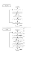
セルフリフレッシュにつき低消費電力化を実現するためには、単純にセルフリフレッシュ周期を長期化し単位時間内に行われるリフレッシュ回数を減らす事が有効であるが、一方でメモリセルのデータ保持可能時間を越えてセルフリフレッシュ周期を長期に設定するとメモリセルのデータは失われ不良を生じてしまうため、データの消失が起こらない程度の適当な値に設定する事が必要とされる。ここで、図1のフローチャートを用いて従来のセルフリフレッシュ方式について説明する。
To achieve low power consumption for self-refresh, it is effective to simply extend the self-refresh cycle and reduce the number of refreshes performed within a unit time. If the self-refresh cycle is set to a long time, the data in the memory cell is lost and defective, so it is necessary to set it to an appropriate value that does not cause data loss. Here, the conventional self-refresh method will be described with reference to the flowchart of FIG.
セルフリフレッシュモードは外部から入力されるコマンドの組合せにより設定され、セルフリフレッシュの開始(セルフリフレッシュエントリ)及び、セルフリフレッシュの解除(セルフリフレッシュエグジット)は共に外部から入力されるコマンドの組合せで設定される。動作は、セルフリフレッシュコントロール回路より出力するロウアドレス及び周期を指定するクロックにより制御され、リフレッシュが行われる度にチップ内部のロウアドレスカウンタを順々に繰り上げて行き、リフレッシュが全てのワード線単位で行われるよう制御される(バーストリフレッシュ)。ここで、消費電力を低減するためセルフリフレッシュ期間内にメモリセルアレイ周辺の電源を落とすモード(ディープパワーダウンモード)も従来より用いられている所である。これはビット線、ワード線等の電源を落とす事でメモリセルにかかる電界を緩和し、メモリセルのデータ保持時間を延ばす事でセルフリフレッシュ周期を延長して消費電力を低減する技術である。但し、セルフリフレッシュの周期を延ばす事はその時間分だけ消費電力の低減に繋がるが、その時間を長くし過ぎるとメモリセルのデータが消失し、製品に不良を生じる点に留意する必要がある。
The self-refresh mode is set by a combination of commands input from the outside, and the start of self-refresh (self-refresh entry) and the release of self-refresh (self-refresh exit) are both set by a combination of commands input from the outside. . The operation is controlled by a row address output from the self-refresh control circuit and a clock for designating the cycle. Each time refresh is performed, the row address counter in the chip is sequentially incremented, and refresh is performed in units of all word lines. Controlled to be performed (burst refresh). Here, in order to reduce power consumption, a mode in which the power supply around the memory cell array is turned off during the self-refresh period (deep power down mode) is also conventionally used. This is a technique for reducing the power consumption by reducing the electric field applied to the memory cell by turning off the power supply of the bit line, the word line, etc., and extending the self-refresh period by extending the data retention time of the memory cell. However, extending the self-refresh cycle leads to a reduction in power consumption by that amount, but it should be noted that if the time is excessively long, the data in the memory cell is lost and the product is defective.
従って、メモリセルのデータを維持出来る範囲でセルフリフレッシュ周期を長期化する、一定の最適周期によって全てのメモリセルに対しセルフリフレッシュを実施する事が理想的である。
Therefore, it is ideal that the self-refresh cycle is extended within a range in which data of the memory cells can be maintained, and the self-refresh is performed on all the memory cells at a certain optimum cycle.
しかし、実際には製造プロセスのばらつき等の理由により、全てのメモリセルのデータ保持時間を均一に製造する事は不可能であり、現実的にはデータ保持不良を避けるべくある程度のマージンをデータ保持時間に対して確保した周期のセルフリフレッシュが行われる。ただし、この場合にもデータが失われるメモリセル(不良メモリセル)の発生を完全に防ぐ事は出来ない。
However, in reality, it is impossible to manufacture the data retention time of all memory cells uniformly due to reasons such as variations in the manufacturing process. In reality, a certain amount of margin is retained to avoid data retention failure. Self-refreshing is performed with a period secured against time. However, even in this case, it is impossible to completely prevent the occurrence of memory cells (bad memory cells) from which data is lost.
そこでこの対策として、チップに冗長メモリセルを予め設けておき、製造後のウエハ良品検査時に不良メモリセルを選別し、これと冗長メモリセルとを切り替える事により当該チップを良品として救済する手段が従来からとられている(リダンダンシによる救済)。
Therefore, as a countermeasure for this, there has conventionally been a means for providing a redundant memory cell in a chip in advance, selecting a defective memory cell at the time of wafer non-defective inspection after manufacture, and relieving the chip as a non-defective product by switching between this and the redundant memory cell. (Relief by redundancy)
しかしながら、ウエハ良品検査時にチップを救済した場合にあってもメモリセルのデータ保持時間、つまりセルフリフレッシュ周期を従来の64[ms]から200[ms]300[ms]と長くしていくにつれ、メモリセルの電荷量が減少し、ソフトエラーや電源レベルの変動等の予期しないノイズにより、ウエハ良品検査後に不良メモリセルを生じる場合がある。
However, even when a chip is relieved during a non-defective wafer inspection, as the memory cell data retention time, that is, the self-refresh cycle is increased from the conventional 64 [ms] to 200 [ms] 300 [ms], the memory In some cases, the amount of charge in the cell decreases, and a defective memory cell is generated after the non-defective wafer inspection due to unexpected noise such as a soft error or a power supply level fluctuation.
一般にこのような不良は少数ビットに対して発生するものであるから、対策として誤り訂正符号(Error Correcting Cord。以下ECCと略す)回路の採用が有効である。
In general, since such a defect occurs with respect to a small number of bits, it is effective to employ an error correcting code (hereinafter abbreviated as ECC) circuit as a countermeasure.
ECC回路は、入力データからパリティ(parity)データを発生させ、両者をメモリセルに
書き込み、読み出し時に入力データ及びパリティデータに対して演算を行い、データの誤りを検出して訂正する回路である。ここでECCの機能については、所定のデータ群につき
複数の誤りを訂正するものは回路規模が極めて大きくなるため現実的でなく、実際には所定の符号長に対して1ビットのみを訂正するハミング符号によるECCが採用されている。
The ECC circuit is a circuit that generates parity data from input data, writes both into a memory cell, performs operations on the input data and parity data at the time of reading, and detects and corrects data errors. Here, with respect to the ECC function, what corrects a plurality of errors per predetermined data group is not practical because the circuit scale becomes extremely large, and in fact, Hamming corrects only one bit for a predetermined code length. ECC by sign is adopted.
しかしながら実際はその程度の誤り訂正規模ではセルフリフレッシュ周期の長期化に十分貢献するには至らず、結局セルフリフレッシュ周期の改善効果は100[ms]から400[ms]程度を限界とするに留まっていた。
However, in reality, such error correction scale does not contribute sufficiently to the extension of the self-refresh cycle, and the improvement effect of the self-refresh cycle is limited to about 100 [ms] to 400 [ms] after all. .
ECC回路自体は当業者にとって自明の所であるが、図8に従来のECC回路図の概要を載せる。ECC回路は主に、外部端子からの入力データにパリティデータを発生させてそれらを符
号化する符号器、符号化した入力データ及びパリティデータをメモリセルに書き込むライトバッファ、メモリセルから読み出された符号化データを増幅するメインアンプ、増幅された符号化データを復号しエラーがあった場合にはエラー訂正を行い訂正後のデータを出力する復号器からなる。
Although the ECC circuit itself is obvious to those skilled in the art, an outline of a conventional ECC circuit diagram is shown in FIG. The ECC circuit mainly generates parity data for input data from an external terminal and encodes them, a write buffer for writing the encoded input data and parity data to the memory cell, and a read from the memory cell. It comprises a main amplifier that amplifies the encoded data, and a decoder that decodes the amplified encoded data and corrects the error if there is an error, and outputs the corrected data.
また、入力データに応じ必要とされるパリティビット数は、公知の次式(ハミングコード(Hamming Code))により決定される。
2k ≧ m+k+1 …(1)
ここで、mは入出力データ数であり、kはパリティビット数である。式(1)に依れば、入
出力データの最小単位であるm=8の場合に必要な最低パリティビット数k=4となる。従ってECCの採用に当たっては、入出力データ8ビット分につき、パリティビットを4ビット以
上設けておく必要がある。
Further, the number of parity bits required according to the input data is determined by a well-known equation (Hamming Code).
2 k ≧ m + k + 1 (1)
Here, m is the number of input / output data, and k is the number of parity bits. According to Equation (1), the minimum number of parity bits k = 4 is required when m = 8, which is the minimum unit of input / output data. Therefore, when adopting ECC, it is necessary to provide 4 or more parity bits for 8 bits of input / output data.
例えば後記特許文献1の図1においてECC回路を用いた半導体記憶装置が提案されている
。当該回路によって入力データに対しパリティビットを発生させ、それらをメモリセルに書き込み、読み出し時には入力データ及びパリティビットに対し演算を行う事で誤りを検出、訂正を行うものである(第1図)。
For example, a semiconductor memory device using an ECC circuit is proposed in FIG. The circuit generates parity bits for input data, writes them to memory cells, and performs operations on the input data and parity bits at the time of reading to detect and correct errors (FIG. 1).
上述した従来のECCを利用した半導体記憶装置において、セルフリフレッシュ周期は約100[ms]から400[ms]へと改善されている。ここで図9にセルフリフレッシュ周期(tREF
)とそれに要する消費電流(Icc6:セルフリフレッシュ電流)のグラフを示す。これによるとセルフリフレッシュ周期が長い程に消費電流値が小さくなる事は自明であり、前述したセルフリフレッシュ周期の改善(セルフリフレッシュ周期を100[ms]から400[ms]に長期化)においては約260μAの消費電流削減が達成される事がわかる。更に、電流削減の効果としては、大まかにセルフリフレッシュ周期1[s]の所で収束が始まっていること
から、現実的には1[s]程度のセルフリフレッシュ周期で不良を起こさない半導体記憶装置を設計する事が合理的である。
In the semiconductor memory device using the conventional ECC described above, the self-refresh cycle is improved from about 100 [ms] to about 400 [ms]. FIG. 9 shows the self-refresh cycle (tREF
) And the required current consumption (Icc6: self-refresh current). According to this, it is obvious that the longer the self-refresh period, the smaller the current consumption value. In the improvement of the self-refresh period described above (the self-refresh period is extended from 100 [ms] to 400 [ms]) It can be seen that a current consumption reduction of 260 μA is achieved. Further, as an effect of current reduction, since convergence starts roughly at a self-refresh cycle of 1 [s], a semiconductor memory device that does not cause a failure in a self-refresh cycle of about 1 [s] in reality. It is reasonable to design
つまり、本発明は回路を複雑化しない事でチップサイズの増加を抑えつつ、セルフリフレッシュ周期を更に長期化する事を可能とする半導体記憶装置を提供する事を目的とするものである。
That is, an object of the present invention is to provide a semiconductor memory device that can further increase the self-refresh cycle while suppressing an increase in chip size without complicating the circuit.
本願に開示される発明は上記目的を達成するため概して以下のように構成される。
The invention disclosed in the present application is generally configured as follows to achieve the above object.
複数のビット線と複数のワード線の交差部にデータ保持のためのリフレッシュを必要とするメモリセルを複数アレイ状に備えたメモリセルアレイを有する半導体記憶装置において、データ保持時間に関する情報を記憶する記憶回路と、所定のアドレスが前記記憶回路にアクセスする事で、ペアリング用メモリセル選択線を出力する選択線出力回路と、電源投入後の予め定められた期間内にメモリセルのデータ保持能力を検査し、検査結果を前記記憶回路に記録する制御回路とを備えている。ここで、ペアリング用とは外部からアクセスされるデータを本来格納するメモリセルとは別に、データ格納用メモリセルを専用に設け、そこに前記データを格納する事でデータの保持を補助する用途のものを言い、以下ペアリング用メモリセル、ペアリング用カラム選択線、ペアリング用ロウ選択線と定義する。詳細は実施例の項にて説明する。
Memory for storing information relating to data retention time in a semiconductor memory device having a memory cell array provided with a plurality of memory cells that require refresh for data retention at intersections of a plurality of bit lines and a plurality of word lines A circuit, a selection line output circuit for outputting a pairing memory cell selection line by accessing the memory circuit by a predetermined address, and a data retention capability of the memory cell within a predetermined period after power-on. And a control circuit for inspecting and recording the inspection result in the storage circuit. Here, in addition to the memory cell that originally stores data accessed from the outside for pairing, a dedicated data storage memory cell is provided, and the data is stored therein to assist data retention. These are hereinafter defined as a pairing memory cell, a pairing column selection line, and a pairing row selection line. Details will be described in the section of the embodiment.
また、本発明に係る半導体記憶装置の他の一態様は、前記記憶回路は前記データ保持能力の検査においてデータ保持能力が低いとされた入力アドレスの各ビットを保持するものであって、前記各ビットと入力アドレスの各ビットを比較する前記選択線出力回路を有し、前記選択線出力回路は前記各ビット同士が一致する場合にはペアリング用選択線を出力し、一致しない場合にはペアリング用選択線を出力しない構成を更に有していても良い。
According to another aspect of the semiconductor memory device of the present invention, the storage circuit holds each bit of an input address that is determined to have a low data holding capability in the data holding capability test. The selection line output circuit for comparing each bit of a bit and an input address, and the selection line output circuit outputs a pairing selection line when the bits match each other; You may further have the structure which does not output the selection line for rings.
また、本発明に係る半導体記憶装置の他の一態様は、前記記憶回路はペアリング用メモリセルの要不要の情報を保持し、前記記憶回路にペアリング用メモリセル要のデータが記憶される場合には、前記記憶回路へのアクセスにより前記選択線出力回路がペアリング用選択線を出力し、不要のデータが記憶される場合には、前記記憶回路へのアクセスにより前記選択線出力回路はペアリング用選択線を出力しない構成を更に有していても良い。
According to another aspect of the semiconductor memory device of the present invention, the storage circuit holds information on necessity of the pairing memory cell, and data on the pairing memory cell is stored in the storage circuit. In this case, the selection line output circuit outputs the pairing selection line by accessing the storage circuit, and when the unnecessary data is stored, the selection line output circuit is accessed by accessing the storage circuit. You may further have the structure which does not output the selection line for pairing.
また、本発明に係る半導体記憶装置の他の一態様は、前記選択線出力回路により出力される選択線がカラム選択線であり、同時に前記選択線出力回路によりペアリング用カラム選択線も出力された場合に、2つのメモリセルのデータに論理和をかけて1つのデータを出力する論理和回路を更に有していても良い。
In another aspect of the semiconductor memory device according to the present invention, the selection line output from the selection line output circuit is a column selection line, and at the same time, a pairing column selection line is output from the selection line output circuit. In this case, a logical sum circuit may be further provided that performs logical sum on the data of two memory cells and outputs one data.
また、本発明に係る半導体記憶装置の他の一態様は、前記選択線出力回路により出力される選択線がロウ選択線である構成を更に有していても良い。
In another aspect of the semiconductor memory device according to the present invention, the selection line output from the selection line output circuit may further include a row selection line.
また、本発明に係る半導体記憶装置の他の一態様においては、符号器及び復号器からなる誤り訂正回路(ECC回路)を有していても良い。
In another embodiment of the semiconductor memory device according to the present invention, an error correction circuit (ECC circuit) including an encoder and a decoder may be included.
また、本発明に係る半導体記憶装置の他の一態様においては、前記予め定められた期間が電源投入後一回目のセルフリフレッシュモードのエントリ時である構成を有していても良い。
In another aspect of the semiconductor memory device according to the present invention, the predetermined period may be a first self-refresh mode entry after power-on.
また、本発明に係る半導体記憶装置の他の一態様においては、前記予め定められた期間が電源投入後のイニシャライズ期間である構成を更に有していても良い。
The semiconductor memory device according to another aspect of the invention may further include a configuration in which the predetermined period is an initialization period after power is turned on.
また、本発明に係る半導体記憶装置の他の一態様においては、前記データ保持時間の検査に際し、ワード線単位で検査対象メモリセルのデータを保持するためのダミーセルを有し、更に前記検査対象メモリセルのデータを前記ダミーセルにコピー後、検査を行い、検査結果を前記記憶回路に記憶し、その後前記ダミーセルのデータを前記検査対象メモリセルにコピーし戻す制御回路を有していても良い。
Further, in another aspect of the semiconductor memory device according to the present invention, a dummy cell for holding the data of the memory cell to be inspected in units of word lines is provided for the inspection of the data holding time, and further the memory to be inspected A control circuit may be provided that performs inspection after copying the cell data to the dummy cell, stores the inspection result in the storage circuit, and then copies the data of the dummy cell back to the memory cell to be inspected.
また、本発明に係る半導体記憶装置の他の一態様においては、前記データ保持検査用のデータとして、メモリセルが物理的に電荷を有する状態になるデータをデータ保持検査対象のワード線に接続するメモリセルに書き込み、その内の所定数単位で前記データ保持検査用データを読み出し、それらの否定論理積(NAND)を取り、その結果からデータ保持能力の有無を検査する制御回路を有していても良い。
In another aspect of the semiconductor memory device according to the present invention, as data for the data retention test, data in which the memory cell is physically charged is connected to a word line to be subjected to the data retention test. It has a control circuit that writes to a memory cell, reads the data holding test data in a predetermined number of units, takes the NAND of them, and checks the presence or absence of data holding capability from the result Also good.
また、本発明に係る半導体記憶装置の使用方法の一態様においては、複数のビット線と複数のワード線の交差部にデータ保持のためのリフレッシュを必要とするメモリセルを複数アレイ状に備えたメモリセルアレイを有する半導体記憶装置において、データ保持時間に関する情報を記憶する記憶回路と、所定のアドレスが前記記憶回路にアクセスする事で、ペアリング用メモリセル選択線を出力する選択線出力回路と、電源投入後の予め定められた期間内にメモリセルのデータ保持能力を検査し、検査結果を前記記憶回路に記録する制御回路とを使用して半導体記憶装置のセルフリフレッシュ制御を行う。
In one aspect of the method of using the semiconductor memory device according to the present invention, a plurality of memory cells that require refresh for data retention are provided in an array at intersections of a plurality of bit lines and a plurality of word lines. In a semiconductor memory device having a memory cell array, a storage circuit that stores information on data retention time, a selection line output circuit that outputs a pairing memory cell selection line by accessing a predetermined address to the storage circuit, The data retention capability of the memory cell is inspected within a predetermined period after the power is turned on, and self refresh control of the semiconductor memory device is performed using a control circuit that records the inspection result in the memory circuit.
また、本発明に係る方法において、前記ダミーセルへのコピーは、検査対象メモリセルにアクセスするワード線を活性化して当該データをセンスアンプで増幅した後、前記ダミーセルにアクセスするワード線を活性化し、前記増幅後のデータを前記ダミーセルへコピーする事により行い、前記ダミーセルからのコピーはこの逆の手順により行う制御を行っても良い。
In the method according to the present invention, the copy to the dummy cell may be performed by activating a word line that accesses the memory cell to be inspected, amplifying the data with a sense amplifier, and activating the word line that accesses the dummy cell, It is possible to perform control by copying the amplified data to the dummy cell, and copying from the dummy cell by the reverse procedure.
また、本発明に係る方法において、前記データ保持能力の検査につき、前記ダミーセルをメモリセルのデータ保持能力に対し十分余裕を持った周期でセルフリフレッシュを行い、且つ検査対象のメモリセルをダミーセルのセルフリフレッシュ周期よりも長い周期でセルフリフレッシュを行っても良い。
Further, in the method according to the present invention, for the test of the data retention capability, the dummy cell is self-refreshed at a period having a sufficient margin for the data retention capability of the memory cell, and the memory cell to be inspected is self-refreshed. Self-refresh may be performed with a period longer than the refresh period.
また、本発明に係る方法において、前記ダミーセルのセルフリフレッシュ周期が100[ms]程度であり、且つ前記検査対象のメモリセルのセルフリフレッシュ周期が1[s]程度
であっても良い。
In the method according to the present invention, the self-refresh cycle of the dummy cell may be about 100 [ms], and the self-refresh cycle of the memory cell to be inspected may be about 1 [s].
本発明によりセルフリフレッシュ周期の長期化が可能となり、チップの消費電力を低減する事が可能となる。同時に、予期しないノイズの発生が製品として組み立てた後であっても当該ノイズに起因するデータの消失等による不良を回避する事が可能となる。
According to the present invention, the self-refresh cycle can be extended and the power consumption of the chip can be reduced. At the same time, it is possible to avoid defects due to loss of data caused by the noise even after unexpected noise has been generated as a product.
既述の本発明を詳述すべく、以下、本発明の原理及び実施例について図面を参照して説明する。
In order to describe the present invention described above in detail, the principle and embodiments of the present invention will be described below with reference to the drawings.
本発明を実施するための最良の形態は、電源投入後のイニシャライズ期間において、ペアリング用メモリセル要不要を選別する形態である。ペアリング用ロウ選択線を用いる事も勿論可能であるが、ここではペアリング用カラム選択線の実施例を挙げる。
The best mode for carrying out the present invention is a mode in which the necessity of pairing memory cells is selected in the initialization period after power-on. Of course, it is possible to use a pairing row selection line, but here, an example of a pairing column selection line will be described.
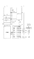
図2は本発明の特徴である電源投入後一回目におけるセルフリフレッシュエントリ後において、ペアリング用メモリセルの要否の選別を行うと共に、要否に応じて従来のカラムアドレス入力に応じるカラム選択線を選別する方法、又はカラムアドレス選択線とペアリング用カラム選択線を選別する方法のフローを表したものである。電源投入後一回目におけるセルフリフレッシュエントリ時には、既にアクセスされたデータが試験対象メモリセルに保持されているため、これを確保すべくダミーセルが必要とされ、当該ダミーセルに試験対象メモリセルのデータをコピーするステップ、コピーしたデータをリフレッシュし保持するステップ、試験後にデータをコピーし戻すステップが必要となる。
FIG. 2 shows a characteristic of the present invention. After the self-refresh entry at the first time after power-on, the necessity of the pairing memory cell is selected and the column selection line according to the conventional column address input according to the necessity. This shows a flow of a method of selecting a column address or a method of selecting a column address selection line and a pairing column selection line. At the first self-refresh entry after power-on, since the already accessed data is held in the test target memory cell, a dummy cell is required to secure this, and the data of the test target memory cell is copied to the dummy cell. A step of refreshing and holding the copied data, and a step of copying back the data after the test.
一方、電源投入後のイニシャライズ期間には試験対象メモリセルにデータは存在しない。このため試験対象メモリセルのデータを保持するためのダミーセルの配置は不要であり、それに伴って前記ダミーセルに絡んだステップは全て不要となる。つまり、イニシャライズ期間に前期選別を行う事で、ダミーセルに絡んだステップS201、S203、S204、S208、S209、S211を削除し回路動作を簡素化する事が出来る。
On the other hand, there is no data in the memory cell to be tested in the initialization period after the power is turned on. For this reason, it is not necessary to dispose dummy cells for holding data of the memory cell to be tested, and accordingly, all steps involved with the dummy cells are unnecessary. In other words, by selecting the previous period during the initialization period, steps S201, S203, S204, S208, S209, and S211 associated with the dummy cell can be deleted, and the circuit operation can be simplified.
図1下は本発明におけるセルフリフレッシュ全体のフローを表したものである。ここで従来例と異なる点は、電源投入後1回目のセルフリフレッシュエントリ後において、ノーマルモード時のカラムアドレスの入力についてカラムアドレスに応じるカラム選択線のみを出力するか、又はカラムアドレスに応じるカラム選択線及びペアリング用カラム選択線を出力するか選別する、ステップS103のみである。その他の動作は従来例と同様であるため説明を省略する。次に、本発明の特徴であるステップS103について図2を参照して説明す
る。
The lower part of FIG. 1 shows the flow of the entire self-refresh in the present invention. Here, the difference from the conventional example is that after the first self-refresh entry after power-on, only the column selection line corresponding to the column address is output for the column address input in the normal mode, or the column selection according to the column address is performed. Only step S103 is performed to select whether to output a line and a column selection line for pairing. Since other operations are the same as those of the conventional example, description thereof is omitted. Next, step S103, which is a feature of the present invention, will be described with reference to FIG.
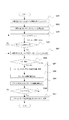
図2は前記S103のフローを表したものである。本発明の特徴であるこのフローは、電源投
入後第一回目におけるセルフリフレッシュエントリ後におけるカラムアドレスに応じるカラム選択線、又はカラム選択線及びペアリング用カラム選択線の選別方法に関する。電源投入後という実動作時の処理にする事で、従来の冗長メモリセルでは対応出来なかった製品製造後のエラーに対処する事を可能としている。以下動作順に説明する。
FIG. 2 shows the flow of S103. This flow, which is a feature of the present invention, relates to a method for selecting a column selection line according to a column address after a self-refresh entry in the first time after power-on, or a column selection line and a pairing column selection line. By performing processing during actual operation after power-on, it is possible to cope with errors after product manufacture that cannot be handled by conventional redundant memory cells. The operation will be described below in the order of operation.
ステップS201はセルフリフレッシュエントリ後、セルフリフレッシュ対象となる1本のワ
ード線によりアクセスされる複数のメモリセル(以下、試験対象メモリセルという)のノーマルモード時に格納されたデータを退避すべく、これらをダミーセルにコピーする手順である。
In step S201, after the self-refresh entry, data stored in the normal mode of a plurality of memory cells (hereinafter referred to as test target memory cells) accessed by a single word line to be self-refreshed are saved. This is a procedure for copying to a dummy cell.
具体的には、セルフリフレッシュの対象となるワード線を活性化し、試験対象メモリセルのデータを其々ビット線に出力、センスアンプにより増幅した後、前記ビット線に接続するダミーセルにアクセスするワード線を活性化し、前記ビット線に出力されたデータをダミーセルに格納する手順である。これにより、試験対象メモリセルのデータをダミーセルにコピーする事が出来る。
Specifically, a word line that activates a word line to be self-refreshed, outputs data of a memory cell to be tested to a bit line, amplifies it by a sense amplifier, and then accesses a dummy cell connected to the bit line Is activated, and the data output to the bit line is stored in a dummy cell. Thereby, the data of the memory cell to be tested can be copied to the dummy cell.
次のステップS202では、試験対象メモリセル全てに対しメモリセルが物理的に電荷を有する状態になるデータ(ハイレベルデータ)を書き込む。これは後のステップにおいてこの電化を目標時間保持出来るかテストを行うための準備である。ECC回路を用いるため、パ
リティデータに対しても同様の書き込みを行う。
In the next step S202, data (high level data) is written in which all the memory cells to be tested are in a state in which the memory cells are physically charged. This is a preparation for testing whether the electrification can be maintained for a target time in a later step. Since the ECC circuit is used, the same writing is performed on the parity data.
次のステップS203では、ダミーセルにつきリフレッシュを行う。ここで、ダミーセルには試験対象メモリセルがノーマルモード時に保持していたデータが格納されているため、確実にこれを保持しておく必要がある。従ってダミーセルのリフレッシュ周期はメモリセルのデータ保持能力につき十分余裕を持たせた値とする事が必要である。本実施例では100
[ms]とするが、実使用上これに限るものではない。
In the next step S203, the dummy cells are refreshed. Here, since the data held by the test target memory cell in the normal mode is stored in the dummy cell, it is necessary to securely hold the data. Therefore, the refresh cycle of the dummy cell needs to be a value with a sufficient margin for the data holding capacity of the memory cell. In this example, 100
[Ms] is used, but it is not limited to this in actual use.
次に、ダミーセルのリフレッシュを10回実施した場合に(ステップS204のYes分岐)ハイ
レベルデータを書き込んだ試験対象メモリセルのデータを読み出す(ステップS205)。ここでは前記データ保持目標時間を1[s]とする関係から10回としているが、目標時間は1
[s]に限るものではなく、回数も可変である。
Next, when the dummy cell is refreshed 10 times (Yes branch in step S204), the data of the test target memory cell in which the high-level data is written is read (step S205). Here, the data retention target time is 10 times because of the relationship of 1 [s], but the target time is 1
It is not limited to [s], and the number of times is variable.
一方、ダミーセルのリフレッシュが10回に満たない場合には(ステップS104のNo分岐)10回までリフレッシュを繰り返す。
On the other hand, when the dummy cell refresh is less than 10 times (No branch in step S104), the refresh is repeated up to 10 times.
次のステップS206では、読み出したハイレベルを期待値とする試験対象メモリセルのデータを否定論理積回路(NAND)にかけ、エラーの検出を行う。ここでは8ビットのノーマル
データ及び4ビットのパリティデータの計12ビットに対し検査を行うべく12入力の否定論
理積回路を用いる。試験対象メモリセルに1[s]のデータ保持能力があるか否か検査するためである。
In the next step S206, the data of the memory cell under test having the read high level as an expected value is applied to a NAND circuit (NAND) to detect an error. Here, a 12-input NAND circuit is used to check a total of 12 bits of 8-bit normal data and 4-bit parity data. This is for checking whether the memory cell to be tested has a data holding capability of 1 [s].
ここで、1本のワード線に対する前記全ての否定論理積回路の出力がロウレベルである場
合には、エラー無しの判定となり(ステップS206のNo:エラーなし:分岐)ダミーセルにコピーしておいたデータを試験対象メモリセルにコピーし、ノーマルモード時の状態に戻す(ステップS210)。コピー手順は試験対象メモリセルのデータをコピーした際と同様である。
Here, if the outputs of all the NAND circuits for one word line are at a low level, it is determined that there is no error (No in step S206: No error: branch) Data copied to the dummy cell Is copied to the memory cell to be tested and returned to the normal mode state (step S210). The copy procedure is the same as when data of the memory cell to be tested is copied.
一方、前記否定論理積回路の出力がハイレベルである場合には、エラー有りの判定となり(ステップS206のYes:エラーあり:分岐)エラーとなったメモリセルにアクセスするカ
ラムアドレスを記憶回路(RAM)に格納する。
記憶回路に格納されたカラムアドレスは、カラム選択線出力回路において入力される任意のカラムアドレスと比較され、一致する場合にはカラム選択線のみならずペアリング用メモリセルを指定するペアリング用カラム選択線も出力され、不一致の場合には入力される任意のカラムアドレスに応じるカラム選択線のみが出力される。
これによって読み出しデータにエラーが存在する(データ保持時間の短い)メモリセルを指定するアドレス入力に対しては、当該アドレスに応じるメモリセルと同時にペアリング用メモリセルにもアクセスする事となる。
On the other hand, when the output of the NAND circuit is at a high level, it is determined that there is an error (Yes in Step S206: Error: Branch). The column address for accessing the memory cell in which the error has occurred is stored in the storage circuit (RAM ).
The column address stored in the storage circuit is compared with an arbitrary column address input in the column selection line output circuit, and if they match, the pairing column that specifies not only the column selection line but also the pairing memory cell A selection line is also output. In the case of a mismatch, only the column selection line corresponding to the input arbitrary column address is output.
As a result, for an address input designating a memory cell in which there is an error in read data (short data retention time), the pairing memory cell is accessed simultaneously with the memory cell corresponding to the address.
次のステップS208、S209では、前記ペアリング用メモリセルに対しダミーセルにコピーしておいたデータをコピーする。
In the next steps S208 and S209, the data copied to the dummy cell is copied to the pairing memory cell.
以上のステップはワード線単位で行われるため、本実施例において1ワード線につきアクセスされるメモリセルが512ビット存在していたとすると、1回のステップにつきノーマ
ルデータ8ビットの処理がなされるため、全部で64回の検査処理がなされる事になる(ス
テップS210のNo分岐)。
Since the above steps are performed in units of word lines, if there are 512 bits of memory cells accessed per word line in this embodiment, normal data 8 bits are processed per step. A total of 64 inspection processes will be performed (No branch in step S210).
1ワード線に対する各ステップが終了した後(ステップS210のYes分岐)、ステップS211
においてダミーセルにコピーしておいたデータを試験対象メモリセルにコピーし、ノーマルモード時の状態に戻す。
After each step for one word line is completed (Yes branch of step S210), step S211
The data copied to the dummy cell is copied to the memory cell to be tested and returned to the normal mode.
以上の工程を踏む事で、目標のデータ保持時間を満たさない(読み出しデータにエラーが存在する)メモリセルへのアクセスには当該メモリセルと同一データを格納するペアリング用メモリセルへのアクセスを付随させ、長周期セルフリフレッシュによるエラーを回避させる事が可能となる。また、ECC回路を同時に適用する事でセルフリフレッシュ周期を
更に長期化する事が可能となる。
By taking the above steps, access to a memory cell that does not meet the target data retention time (an error exists in the read data) requires access to a pairing memory cell that stores the same data as the memory cell. In addition, it is possible to avoid errors due to long-cycle self-refresh. Further, by applying the ECC circuit at the same time, the self-refresh cycle can be further extended.
但し、ペアリング用メモリセルについてはダミーセル同様確実な記憶保持を要求する事からセルフリフレッシュ周期をメモリセルのデータ保持能力につき十分余裕を持たせた値とする事が必要である。このペアリング用メモリセルによって、長周期セルフリフレッシュにより発生する試験対象メモリセルのエラーを補償するためである。
However, since the memory cell for pairing requires a reliable memory retention like the dummy cell, it is necessary to set the self-refresh cycle to a value with a sufficient margin for the data retention capability of the memory cell. The purpose of this pairing memory cell is to compensate for errors in the memory cell under test caused by long-period self-refresh.
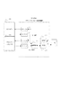
図3は図1及び2のフローを実現する本発明の1実施例の構成を表したものであり、クロック同期型DRAMに本発明を適用したものであり、図中における×8、×12等の記載は信号のビ
ット数を表すものである。
FIG. 3 shows the configuration of one embodiment of the present invention that realizes the flow of FIGS. 1 and 2, in which the present invention is applied to a clock synchronous DRAM. Represents the number of bits of the signal.
図3を参照すると、本発明の1実施例の半導体記憶装置は、ビット線とワード線の交差部にメモリセルを有するメモリセルアレイで構成されるバンク100と、ロウアドレスをデコー
ドし、ワード線を駆動するワードドライバを有するロウデコーダ101と、メモリセルアレ
イ100のビット線に接続するセンスアンプ102を備えている。ここで、バンク100のメモリ
セルアレイには、データ保持試験時に試験対象となるメモリセルのデータをコピーしておくためのダミーセル103、試験の結果でデータ保持時間が短いと判定されたメモリセルの
データを補償するために用いるペアリング用メモリセル104を含んでいる。更に本発明の1実施例の半導体記憶装置はロウアドレスを入力するロウアドレスバッファ105、カラムア
ドレスを入力するカラムアドレスバッファ106と、カラムアドレスデコーダ107と、DRAMの各動作をコントロールするコマンド信号を出力するコマンドデコーダ108と、チップ内部
で各信号を同期するクロックを発生する内部クロック発生器109と、外部とデータの入出
力を制御するデータコントロール回路110と、セルフリフレッシュのアドレス及び周期を
制御するセルフリフレッシュコントロール回路111を備えている。ここで、セルフリフレ
ッシュコントロール回路111はリフレッシュのロウアドレスを指定するアドレスカウンタ
とリフレッシュ周期発生器とを含んでいる。また、リフレッシュ周期発生器においては温度特性を考慮してリフレッシュ周期を設定する温度補正器を含む事としても良い。更に本発明の1実施例の半導体記憶装置は、入力データに対し検査ビットを付加する符号器112と、符号化された出力データを復号しエラー検出を行う復号器113からなるECC回路と、1つ
のアドレスの入力につきメモリセル及びペアリング用メモリセルから出力があった場合に論理和をとって出力する論理和回路114を含んでおり、ECC回路によりエラーが検出された場合のカラムアドレスを保持するレジスタ117と、レジスタ117のデータを格納する記憶回路115、記憶回路115にアクセスしてカラム選択線及びペアリング用カラム選択線を出力するカラムアドレス比較回路116を設けている。
Referring to FIG. 3, a semiconductor memory device according to an embodiment of the present invention includes a
チップ外部からのコマンド制御信号としては、チップセレクト信号/CS、ロウアドレスストローブ信号/RAS、カラムアドレスストローブ信号/CAS、ライトイネーブル信号/WEが入力され、チップ内部の各動作をコントロールする。またCLKは同期用の外部クロック信
号であり、CKEはCLKの有効、無効を決定するクロックイネーブル信号である。CKEがロウ
レベルである場合には、CLKは無効とされ、チップはスタンバイ状態とされる。DQMはDQの入出力マスク信号であり、DQはチップへ書き込み、またはチップから読み出す入出力データを指す。
As command control signals from the outside of the chip, a chip select signal / CS, a row address strobe signal / RAS, a column address strobe signal / CAS, and a write enable signal / WE are input to control each operation inside the chip. CLK is an external clock signal for synchronization, and CKE is a clock enable signal that determines whether CLK is valid or invalid. When CKE is at a low level, CLK is invalidated and the chip is in a standby state. DQM is a DQ input / output mask signal, and DQ indicates input / output data to be written to or read from the chip.
図2のフローに則して図3の構成を説明すると、まずセルフリフレッシュエントリのコマ
ンド制御信号が入力され、CKEがロウレベルで入力し保持される事によりセルフリフレッ
シュエントリが行われる。次に、セルフリフレッシュコントロール回路111は、セルフリ
フレッシュの周期及びロウアドレスを発生し、ロウデコーダ101に出力する。ロウデコー
ダ101に入力されたロウアドレスは図示しないワードドライバによりワード線を出力し、
当該ワード線によりアクセスされる全ての試験対象メモリセルのデータをビット線に出力、続いてこれらデータをセンスアンプ102により増幅する。続いて同じくセルフリフレッ
シュコントロール回路111によりダミーセル103のロウアドレスをロウデコーダ101に出力
、同様の手段によりダミーセル103にアクセスし、既に増幅されたビット線各々のデータ
をダミーセル103に書き込む。これにより前記試験対象メモリセルのデータのダミーセル
へのコピーが行われる。
The configuration of FIG. 3 will be described in accordance with the flow of FIG. 2. First, the command control signal of the self-refresh entry is input, and the self-refresh entry is performed by inputting and holding CKE at the low level. Next, the self-refresh control circuit 111 generates a self-refresh cycle and a row address, and outputs them to the
Data of all test target memory cells accessed by the word line is output to the bit line, and then the data is amplified by the
コピー後は更に試験対象メモリセルにアクセスするワード線をアクティブとし、全ての試験対象メモリセルにハイレベルデータを書き込んでおく。
After copying, the word line for accessing the memory cell to be tested is further activated, and high level data is written to all the memory cells to be tested.
次にセルフリフレッシュコントロール回路111によりダミーセル103部についてはメモリセルのデータ保持能力に対し十分余裕を持たせた周期でリフレッシュを行い(本実施例では100[ms])、一方試験対象メモリセル部についてはリフレッシュ周期を長期化した値(
本実施例では1[s])に周期を設定する。ノーマルモード時に格納されたメモリセルのデータをダミーセル103に確実に保持しつつ、試験対象メモリセルの保持するハイデータに
ついてデータ保持能力を試験するためである。
Next, the self-refresh control circuit 111 refreshes the
In this embodiment, the period is set to 1 [s]). This is for testing the data holding capability of the high data held by the memory cell to be tested while reliably holding the data of the memory cell stored in the normal mode in the
1[s]経過後には通常の読み出し方法により試験対象メモリセルのデータ12ビット1単位
をビット線に出力(既述の通り、ここではノーマルデータ8ビット及びパリティデータ4ビットの計12ビットとする)、センスアンプ102により増幅し、図示しないデータ入出力線
に出力し、図示しない否定論理積回路(NAND)に入力し、エラー判定を行う。各ビットの期待値は全てハイレベルデータであるから、否定論理積回路(NAND)の出力がロウレベルデータの場合はエラー無しの判定であり、出力がハイレベルデータである場合はエラー有りの判定となる。
After 1 [s], the unit of 12 bits of data of the memory cell to be tested is output to the bit line by the normal reading method (as described above, here, the normal data is 8 bits and the parity data is 4 bits, which is 12 bits in total) ), Amplified by the
エラー判定された場合には当該エラーとなったカラムアドレスをカラムアドレスバッファ106より記憶回路115に格納し、一方、エラー判定がされない場合にはカラムアドレスの書き込みは行わない。
If an error is determined, the column address in error is stored in the
記憶回路115に格納されたカラムアドレスは、それに一致するカラムアドレスがカラムア
ドレス比較回路116へ入力する事によりカラムアドレスにより指定されるカラム選択線の
みでなくペアリング用カラム選択線をも出力する役割を果たすものである。
The column address stored in the
次に、ノーマルモード時に格納したダミーセル103のデータを試験対象メモリセルにコピ
ーし戻す。ダミーセルへのコピーにおいては試験対象メモリセルのデータをセンスアンプ102にて増幅の後、ダミーセルにアクセスしデータを書き込んだが、ここでは逆に、ダミ
ーセルのデータをセンスアンプ102にて増幅の後、試験対象メモリセルにアクセスしデー
タを書き込む。またこの際に、記憶回路115に格納したカラムアドレスにより、ペアリン
グ用メモリセル104に対しても該当するダミーセル103のデータを書き込んでおく。データ保持時間が短いと判定されたメモリセルのデータを補償するためである。
Next, the data in the
以上のプロセスにより試験対象メモリセルのデータはノーマルアクセス時の状態に戻り、またデータ保持時間の短いメモリセルに対しては、それを補うペアリング用メモリセルがあてがわれ、前記データ保持時間の短いメモリセルと同一データが書き込まれる。以上の構造、工程により電源投入後第1回目のセルフリフレッシュが行われる。
Through the above process, the data of the memory cell to be tested is returned to the normal access state, and a memory cell with a short data holding time is assigned a pairing memory cell to compensate for the data holding time. The same data as the short memory cell is written. With the above structure and process, the first self-refresh is performed after the power is turned on.
次に外部からのデータ書き込みについて同じく図3を利用して説明する。
Next, data writing from the outside will be described with reference to FIG.
外部データは従来同様DQより入力、データコントロール回路110により制御される。本実
施例においてはECC回路を利用するため、入力データは符号器112に入力されパリティデータを付加した符号化データとして出力される。最終的に前記符号化データはカラムデコーダ107及びロウデコーダ101で指定するカラムアドレス、ロウアドレスに対応したメモリセルアレイ100の内の該当箇所に書き込まれる。ここで、カラムアドレスバッファ106より指定されるカラムアドレスがカラムアドレス比較回路116により記憶回路115に格納するカラムアドレスと一致するとの判定をされた場合には、カラムデコーダ107はカラムアドレス
に応じるカラム選択線だけでなくペアリング用メモリセルを選択するカラム選択線も出力する。これにより1つの外部データをペアリング用メモリセルに対しても格納する事が出来る。
External data is input from the DQ and controlled by the
次に内部からのデータ読み出しについて同じく図3を利用して説明する。
Next, data reading from the inside will be described with reference to FIG.
読み出しの場合もメモリセルの特定までは書き込みと同様の動作である。また、カラムアドレスがカラムアドレス比較回路116により記憶回路115に格納するカラムアドレスと一致する判定をされた場合には書き込み時同様にカラム選択線及びペアリング用カラム選択線が出力され、対応したメモリセル及びペアリング用メモリセルに格納されたデータを出力する。これら出力された2のデータは其々センスアンプ102にて増幅後、論理和回路114に
より論理和をとり、1つの出力データとされ、データコントロール回路110を経由してDQパッドから外部へ出力される。
ここで前記2つのメモリセルからデータを出力するのは既述の通り、セルフリフレッシュ
周期の長期化による不良をペアリング用メモリセルのデータにより補償するためであるが、論理和回路114を用いるのは、ハイレベルの期待値に対し出力がロウレベル(エラー)
が出力される場合のみを考慮する事による。実際にセルフリフレッシュ長期化によるエラーはハイレベルデータがロウレベルデータに失われる状況のみを考慮する事で足りるからである。
また、ペアリング用メモリセルについてはセルフリフレッシュ周期を十分短くしている事からデータ保持に問題はなく、従って、長く設定したセルフリフレッシュ周期によりデータを失ったメモリセルがあっても、ペアリング用メモリセルのデータと論理和をとる事でデータ保持不良を防止する事が可能である。
In the case of reading, the operation is the same as that of writing until the memory cell is specified. If the column
Here, as described above, the data is output from the two memory cells in order to compensate the defect due to the prolonged self-refresh cycle by the data of the memory cell for pairing, but the OR
By considering only when. This is because the error due to the prolonged self-refresh is actually considered only by considering the situation where the high level data is lost to the low level data.
In addition, since the self-refresh cycle is sufficiently shortened for the pairing memory cell, there is no problem in data retention. Therefore, even if there is a memory cell that has lost data due to a long self-refresh cycle, it is for pairing. It is possible to prevent data retention failure by taking a logical OR with the data in the memory cell.
以上の構造、工程における、データ保持時間の短いメモリセルを検出し同時にそれを補うペアリング用メモリセルを設ける事でデータ保持不良を防止しつつ、セルフリフレッシュ周期を長期化する事が出来る。
In the above structure and process, a self-refresh cycle can be prolonged while preventing a data retention failure by providing a pairing memory cell that detects a memory cell having a short data retention time and simultaneously compensates for it.
次に、本発明の特徴である、ペアリング用メモリセル104の動作、カラムアドレス比較
回路116、論理和回路114について各々図を用いて詳細に説明する。
Next, the operation of the
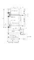
図4は図3におけるペアリング用メモリセル104及びその周辺回路を表示した拡大図で
ある。以下、図4を用いてペアリング用メモリセル104の読み出し動作と書き込み動作に
ついて説明する。
FIG. 4 is an enlarged view showing the
読み出し動作及び書き込み動作は、図示しないコマンドデコーダ108により出力される
コマンド信号により制御される。コマンド信号はロウデコーダ101、カラムアドレス比較
回路116に入力し、それぞれをアクティブとする。その後アドレス信号の入力を受け、ロ
ウアドレスはメインワードドライバーによりメインワード線を出力し更にメインワード線はメモリセルアレイ100内のサブワードドライバーを活性化する事でワード線を出力しメ
モリセルにアクセスする。ここでメインワード線はペアリング用メモリセルに対しても共通とされ、ペアリング用メモリセルにも同時にアクセスする構造である。一方、カラムアドレスはカラムアドレス比較回路116へ入力し、コマンド信号の入力により記憶回路115に格納されたカラムアドレスと比較され、一致した場合には本来のカラムアドレスに応じたカラム選択線と同時にペアリング用メモリセルを指定するカラム選択線も出力する。この2つのカラム選択線によって、2つのメモリセルに対する読み出し動作、書き込み動作を同時に行う事が可能となる。
A read operation and a write operation are controlled by a command signal output from a command decoder 108 (not shown). The command signal is input to the
図5は図3におけるカラムアドレス比較回路116及びその周辺回路を表示した拡大図で
ある。以下、図5を用いてカラムアドレス比較回路116の動作について説明する。
FIG. 5 is an enlarged view showing the column
カラムアドレス比較回路116は、入力されたカラムアドレスが記憶回路115に格納されているか比較し、一致する場合には本来のカラムアドレスに応じたカラム選択線とペアリング用メモリセルを指定するカラム選択線も出力するものである。図5の実施例として、ペアリング用メモリセル104の数を1メインワードにつき、ノーマルビット8ビットとパリティビット4ビットの計12ビットを5セット用意した60ビットとしておく。これは1メインワードにつきデータ保持時間が短いと判定されたメモリセルを5箇所補償出来る事を意味す
る。当該ビット数はこれに限るものではないが、データ保持時間の短いメモリセルは非常に少数であるという実験結果に照らせば十分である。また、ペアリング用メモリセルを多くすればその分チップサイズの拡大に繋がるため、出来るだけ少なく抑える事が望ましい。
The column
本実施例ではカラムアドレスを構成するビットをY0~Y9の10ビットとし、記憶回路115に格納された事を示す1ビットを加え、更にこれを5セット用意する事から、記憶回路115か
らカラムアドレス比較回路116には計55ビットのデータが転送される。ここで、ペアリン
グ用メモリセルが割り当てられている場合には、R1(E)〜R5(E)にハイデータが書き込まれる事とし、読み出し動作又は書き込み動作時にまずはR(E)を比較確認回路によってチェックし、ハイデータである場合に限りY0~Y9までのカラムアドレスを比較する。一致した場
合には、R(E)を除いた10ビットがペアリング用メモリセルのカラムアドレスとして出力され、カラムデコーダ104によりペアリング用メモリセルを指定するペアリング用カラム選
択線を出力する。また、同時に本来のカラムアドレスに応じたカラム選択線もカラムデコーダ104により出力されるため、同時に2つのメモリセルにアクセスする事が可能となる
。
In this embodiment, the bits constituting the column address are 10 bits Y0 to Y9, 1 bit indicating that the bit is stored in the
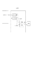
図6は図3における論理和回路及びその周辺回路を表示した拡大図である。以下、図6を用いて論理和回路等の動作について説明する。
FIG. 6 is an enlarged view showing the OR circuit and its peripheral circuits in FIG. Hereinafter, the operation of the OR circuit and the like will be described with reference to FIG.
図6において、DQから入力されたデータは符号器112によりパリティデータ(DQの入力
が8ビットである場合、パリティビットは4ビット)を付加しライトバッファを経由してメモリセルアレイ100内のメモリセルに格納される。ここで、所定のカラムアドレスにつ
いては、既述の通りペアリング用メモリセル104にも同じデータが格納される。一方、所
定のカラムアドレスに対する読み出し時には、2つのデータが同時に出力される事となるが、それぞれから読み出されるデータは1つにまとめる必要があるため、本発明の特徴の一つである論理和回路114を用いている。具体的には12ビットの各桁それぞれに対する論
理和回路(OR回路)となる。符号器112、復号器113については公知のECC回路と同様の構
成である。
In FIG. 6, the data input from the DQ is added with parity data (when the DQ input is 8 bits, the parity bit is 4 bits) by the
以上、本発明の実施例を説明したが、以下ペアリング用ロウ選択線の実施例についても加えておく。
Although the embodiment of the present invention has been described above, the embodiment of the pairing row selection line will be added below.
ペアリング用ロウ選択線の選別方法の動作に関するフローは図2において、カラムアドレスをロウアドレスに読み替える事でほぼ足りる。但し、実際にメモリセルにアクセスするロウ選択線とはワード線であるからペアリング用ロウ選択線の要不要を判定する記憶回路115はサブワードドライバーの選択に属するものである事が妥当である。また、サブワ
ードドライバーにおいて通常メモリセルを選択する全てのロウアドレスはデコードが済んでいるため、カラムの場合の様に記憶回路にカラムアドレスの各ビットを記録し、入力されるカラムアドレスと比較する必要はなく、当該選択されるワード線にペアリング用ロウ選択線が必要か否か及びどこのペアリング用ロウ選択線を用いるかの情報が存在している事で足りる。この点においてカラム選択線の場合と異なるが、カラム側についても同様の回路構成とする事は可能で、逆にロウ側について記憶回路にロウアドレスを格納する手段をとる事も可能である。この点は設計事項として選択可能である。
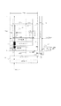
The flow relating to the operation of the method of selecting the pairing row selection line is almost sufficient by replacing the column address with the row address in FIG. However, since the row selection line that actually accesses the memory cell is a word line, it is appropriate that the
図7は本発明においてペアリング用ロウ選択線を使用する場合のメモリセルアレイ周りの回路を表示した拡大図である。基本的にペアリング用メモリセル使用時は、通常メモリセルのワード線とペアリング用メモリセルのワード線を同時に選択し、双方のメモリセルデータをビット線上に合成して読み出す構成をとる。図7の実施例では、ダミーセル103とペアリング用メモリセル104を共用した構成としている。つまりデータ保持能力の検査時
においてはダミーセル103として利用し、その後はペアリング用メモリセル104として使用する構成である。但し、この場合においてはカラムの場合に紹介した例とは異なり、データ保持能力の検査時にペアリング用メモリセルへのコピーは出来ないため、検査終了後に順次データ保持能力が低いメモリセルのデータをペアリング用メモリセルにコピーしていく流れとなる。この場合においてはコピー先であるペアリング用ロウ選択線がコピー元であるワード線よりも後でアクティブ状態となるよう、ペアリング用ロウ選択線側に遅延回路等を設けておく事がエラー消失防止のために必須である。他、エラー判定の方法等については前記カラム選択線の場合と同様であるため説明を省略する。
FIG. 7 is an enlarged view showing a circuit around the memory cell array when the pairing row selection line is used in the present invention. Basically, when the pairing memory cell is used, the word line of the normal memory cell and the word line of the pairing memory cell are selected at the same time, and both the memory cell data are synthesized on the bit line and read. In the embodiment of FIG. 7, the
エラー判定結果はカラムレジスタ117により特定されるカラムアドレスに従い、記憶回路115に書き込まれる。ここで、記憶回路115は各サブワードドライバーに設けられ、ペアリ
ング用ロウ選択線を用いるか用いないか、及び、どのペアリング用ロウ選択線にアクセスするか、の情報を格納する。例として16bitのワード線に1対1対応すべく16bitの記憶回路を各ワード線に割り当てる事とする。次に、記憶回路115はサブワードドライバーに付
属するため、ワード線を選択するロウアドレスの入力がされる事で同時に記憶回路115に
もアクセスされ、記憶回路115に格納されるデータに基づきワード線と共にペアリング用
ロウ選択線も出力される。これにより一本のカラム選択線につき、同時に2つのメモリセルにアクセスする事が可能となる。ここで、2本のカラム選択線により2つのデータを出力するペアリング用カラム選択線の場合と異なり、ペアリング用ロウ選択線を用いる場合には1本のカラム選択線により2つのデータを出力し、2つのデータは共通のビット線により合成される事から、図3における論理和回路114は必要とされない構成である。
The error determination result is written in the
尚、ワード線単位でペアリング用ロウ選択線を出力する事から、実際にデータ保持能力が低いメモリセルのみでなく能力が十分にあるメモリセルに対してもペアリング用メモリセルが選択される事になるのでデータが反転することはない。逆に、この場合には共通のビット線にのる微小電圧が増加(単純にはメモリセル2つ分なので2倍)され、センスアンプによるセンス時間、センスマージンを改善する副次的効果を有する。
Since the pairing row selection line is output in units of word lines, pairing memory cells are selected not only for memory cells with actually low data holding capability but also for memory cells with sufficient capability. The data will never be reversed. On the contrary, in this case, the minute voltage on the common bit line is increased (simply twice because it is equivalent to two memory cells), and has a secondary effect of improving the sense time and sense margin by the sense amplifier. .
以上、本発明の動作、構成について説明したが、本発明は既述の実施例に限定されるものではなく、当業者であれば容易に思いつく変更、修正を含む事は勿論である。
The operation and configuration of the present invention have been described above. However, the present invention is not limited to the above-described embodiments, and of course includes changes and modifications that can be easily conceived by those skilled in the art.
100 メモリセルアレイ(ダミーセル、ペアリング用メモリセル含む)
101 ロウデコーダ
102 センスアンプ
103 ダミーセル
104 ペアリング用メモリセル
105 ロウアドレスバッファ
106 カラムアドレスバッファ
107 カラムデコーダ
108 コマンドデコーダ
109 内部クロック発生器
110 データコントロール回路
111 セルフリフレッシュコントロール回路
112 符号器
113 復号器
114 論理和回路
115 記憶回路
116 カラムアドレス比較回路
117 レジスタ
100 memory cell array (including dummy cells and pairing memory cells)
101 Row decoder
102 sense amplifier
103 dummy cell
104 Memory cell for pairing
105 Row address buffer
106 Column address buffer
107 column decoder
108 Command decoder
109 Internal clock generator
110 Data control circuit
111 Self-refresh control circuit
112 encoder
113 Decoder
114 OR circuit
115 Memory circuit
116 Column address comparison circuit
117 registers
Claims (14)
Memory for storing information relating to data retention time in a semiconductor memory device having a memory cell array provided with a plurality of memory cells that require refresh for data retention at intersections of a plurality of bit lines and a plurality of word lines A circuit, a selection line output circuit for outputting a pairing memory cell selection line by accessing the memory circuit by a predetermined address, and a data retention capability of the memory cell within a predetermined period after power-on. A semiconductor memory device comprising: a control circuit that inspects and records an inspection result in the memory circuit.
前記記憶回路は前記データ保持能力の検査においてデータ保持能力が低いとされた入力アドレスの各ビットを保持するものであって、前記各ビットと入力アドレスの各ビットを比較する前記選択線出力回路を有し、前記選択線出力回路は前記各ビット同士が一致する場合にはペアリング用選択線を出力し、一致しない場合にはペアリング用選択線を出力しない事を特徴とする請求項1記載の半導体記憶装置。
The memory circuit holds each bit of an input address whose data holding capability is low in the test of the data holding capability, and the selection line output circuit for comparing each bit with each bit of the input address The selection line output circuit outputs a pairing selection line when the bits match, and does not output a pairing selection line when they do not match. Semiconductor memory device.
前記記憶回路はペアリング用メモリセルの要不要の情報を保持し、前記記憶回路にペアリング用メモリセル要のデータが記憶される場合には、前記記憶回路へのアクセスにより前記選択線出力回路がペアリング用選択線を出力し、不要のデータが記憶される場合には、前記記憶回路へのアクセスにより前記選択線出力回路はペアリング用選択線を出力しない事を特徴とする請求項1記載の半導体記憶装置。
The memory circuit holds unnecessary information on the pairing memory cell, and when the data necessary for the pairing memory cell is stored in the memory circuit, the selection line output circuit is accessed by accessing the memory circuit. 2. When a pairing selection line is output and unnecessary data is stored, the selection line output circuit does not output a pairing selection line by accessing the storage circuit. The semiconductor memory device described.
前記選択線出力回路により出力される選択線がカラム選択線であり、同時に前記選択線出力回路によりペアリング用カラム選択線も出力された場合に、2つのメモリセルのデータに論理和をかけて1つのデータを出力する論理和回路を有する事を特徴とする請求項1乃至3記載の半導体記憶装置。
When the selection line output from the selection line output circuit is a column selection line and at the same time the pairing column selection line is also output from the selection line output circuit, the data of two memory cells are logically summed. 4. The semiconductor memory device according to claim 1, further comprising an OR circuit that outputs one data.
前記選択線出力回路により出力される選択線がロウ選択線である事を特徴とする請求項1乃至3記載の半導体記憶装置。
4. The semiconductor memory device according to claim 1, wherein the selection line output from the selection line output circuit is a row selection line.
符号器及び復号器からなる誤り訂正回路(ECC回路)を有する事を特徴とする請求項1乃
至5記載の半導体記憶装置。
6. The semiconductor memory device according to claim 1, further comprising an error correction circuit (ECC circuit) comprising an encoder and a decoder.
前記予め定められた期間が電源投入後一回目のセルフリフレッシュモードのエントリ時である事を特徴とする請求項1乃至6記載の半導体記憶装置。
7. The semiconductor memory device according to claim 1, wherein the predetermined period is a first self-refresh mode entry after power-on.
前記予め定められた期間が電源投入後のイニシャライズ期間である事を特徴とする請求項1乃至6記載の半導体記憶装置。
7. The semiconductor memory device according to claim 1, wherein the predetermined period is an initialization period after power is turned on.
前記データ保持時間の検査に際し、ワード線単位で検査対象メモリセルのデータを保持するためのダミーセルを有し、更に前記検査対象メモリセルのデータを前記ダミーセルにコピー後、検査を行い、検査結果を前記記憶回路に記憶し、その後前記ダミーセルのデータを前記検査対象メモリセルにコピーし戻す制御回路を有する事を特徴とする請求項1乃至8記載の半導体記憶装置。
When inspecting the data retention time, it has a dummy cell for holding data of the memory cell to be inspected in units of word lines, and further inspects the data after the data of the memory cell to be inspected is copied to the dummy cell. 9. The semiconductor memory device according to claim 1, further comprising a control circuit that stores the data in the memory circuit and then copies the data of the dummy cell back to the memory cell to be inspected.
前記データ保持検査用のデータとして、メモリセルが物理的に電荷を有する状態になるデータをデータ保持検査対象のワード線に接続するメモリセルに書き込み、その内の所定数単位で前記データ保持検査用データを読み出し、それらの否定論理積(NAND)を取り、その結果からデータ保持能力の有無を検査する制御回路を有する事を特徴とする請求項1乃
至9記載の半導体記憶装置。
As the data retention test data, data that causes the memory cell to have a physical charge is written to the memory cell connected to the word line to be subjected to the data retention test, and the data retention test is performed in a predetermined number of the data. 10. The semiconductor memory device according to claim 1, further comprising a control circuit that reads out data, takes a negative logical product (NAND) of the data, and inspects the presence / absence of data holding capability based on the result.
複数のビット線と複数のワード線の交差部にデータ保持のためのリフレッシュを必要とするメモリセルを複数アレイ状に備えたメモリセルアレイを有する半導体記憶装置において、データ保持時間に関する情報を記憶する記憶回路と、所定のアドレスが前記記憶回路にアクセスする事で、ペアリング用メモリセル選択線を出力する選択線出力回路と、電源投入後の予め定められた期間内にメモリセルのデータ保持能力を検査し、検査結果を前記記憶回路に記録する制御回路とを使用する半導体記憶装置のセルフリフレッシュ制御方法。
Memory for storing information relating to data retention time in a semiconductor memory device having a memory cell array provided with a plurality of memory cells that require refresh for data retention at intersections of a plurality of bit lines and a plurality of word lines A circuit, a selection line output circuit for outputting a pairing memory cell selection line by accessing the memory circuit by a predetermined address, and a data retention capability of the memory cell within a predetermined period after power-on. A self-refresh control method for a semiconductor memory device using a control circuit that inspects and records a test result in the memory circuit.
前記ダミーセルへのコピーは、検査対象メモリセルにアクセスするワード線を活性化して当該データをセンスアンプで増幅した後、前記ダミーセルにアクセスするワード線を活性化し、前記増幅後のデータを前記ダミーセルへコピーする事により行い、前記ダミーセルからのコピーはこの逆の手順により行う事を特徴とする請求項11記載の半導体記憶装置のセルフリフレッシュ制御方法。
In copying to the dummy cell, the word line for accessing the memory cell to be inspected is activated and the data is amplified by a sense amplifier, the word line for accessing the dummy cell is activated, and the amplified data is transferred to the dummy cell. 12. The self-refresh control method for a semiconductor memory device according to claim 11, wherein copying is performed by copying, and copying from the dummy cell is performed by the reverse procedure.
前記データ保持能力の検査につき、前記ダミーセルをメモリセルのデータ保持能力に対し十分余裕を持った周期でセルフリフレッシュを行い、且つ検査対象のメモリセルをダミーセルのセルフリフレッシュ周期よりも長い周期でセルフリフレッシュを行う請求項11記載の半導体記憶装置のセルフリフレッシュ制御方法。
For testing the data retention capability, the dummy cells are self-refreshed at a cycle having a sufficient margin for the data retention capability of the memory cells, and the memory cells to be tested are self-refreshed at a cycle longer than the self-refresh cycle of the dummy cells. 12. The self-refresh control method for a semiconductor memory device according to claim 11, wherein:
前記ダミーセルのセルフリフレッシュ周期が100[ms]程度であり、且つ前記検査対象の
メモリセルのセルフリフレッシュ周期が1[s]程度とする事を特徴とする請求項13記載の半導体記憶装置のセルフリフレッシュ制御方法。
14. The self-refresh of a semiconductor memory device according to claim 13, wherein a self-refresh period of the dummy cell is about 100 [ms], and a self-refresh period of the memory cell to be inspected is about 1 [s]. Control method.
Priority Applications (2)
| Application Number | Priority Date | Filing Date | Title |
|---|---|---|---|
| JP2004110814A JP2005293785A (en) | 2004-04-05 | 2004-04-05 | Semiconductor memory device and its self-refresh control method |
| US11/097,247 US7158433B2 (en) | 2004-04-05 | 2005-04-04 | Semiconductor storage device and method of controlling refreshing of semiconductor storage device |
Applications Claiming Priority (1)
| Application Number | Priority Date | Filing Date | Title |
|---|---|---|---|
| JP2004110814A JP2005293785A (en) | 2004-04-05 | 2004-04-05 | Semiconductor memory device and its self-refresh control method |
Publications (1)
| Publication Number | Publication Date |
|---|---|
| JP2005293785A true JP2005293785A (en) | 2005-10-20 |
Family
ID=35054097
Family Applications (1)
| Application Number | Title | Priority Date | Filing Date |
|---|---|---|---|
| JP2004110814A Pending JP2005293785A (en) | 2004-04-05 | 2004-04-05 | Semiconductor memory device and its self-refresh control method |
Country Status (2)
| Country | Link |
|---|---|
| US (1) | US7158433B2 (en) |
| JP (1) | JP2005293785A (en) |
Cited By (1)
| Publication number | Priority date | Publication date | Assignee | Title |
|---|---|---|---|---|
| US8874996B2 (en) | 2011-10-27 | 2014-10-28 | Samsung Electronics Co., Ltd. | Memory device having reconfigurable refresh timing |
Families Citing this family (17)
| Publication number | Priority date | Publication date | Assignee | Title |
|---|---|---|---|---|
| US7286432B2 (en) * | 2005-07-22 | 2007-10-23 | Infineon Technologies Ag | Temperature update masking to ensure correct measurement of temperature when references become unstable |
| JP2007066423A (en) * | 2005-08-31 | 2007-03-15 | Toshiba Corp | Semiconductor integrated circuit device |
| US7362640B2 (en) * | 2005-12-29 | 2008-04-22 | Mosaid Technologies Incorporated | Apparatus and method for self-refreshing dynamic random access memory cells |
| KR100810060B1 (en) | 2006-04-14 | 2008-03-05 | 주식회사 하이닉스반도체 | Semiconductor memory device and driving method thereof |
| US7773441B2 (en) * | 2008-06-18 | 2010-08-10 | Micron Technology, Inc. | Memory malfunction prediction system and method |
| US8705302B2 (en) | 2010-09-24 | 2014-04-22 | Samsung Electronics Co., Ltd. | Semiconductor memory devices having self-refresh capability |
| KR101861647B1 (en) * | 2011-05-24 | 2018-05-28 | 삼성전자주식회사 | Memory system and refresh control method thereof |
| KR20120132287A (en) * | 2011-05-27 | 2012-12-05 | 삼성전자주식회사 | Semiconductor memory device, semiconductor memory package, and method of increasing density of a semiconductor memory device |
| JP2012252530A (en) * | 2011-06-03 | 2012-12-20 | Fujitsu Ltd | Memory controller and control method |
| US9640240B2 (en) | 2013-11-26 | 2017-05-02 | Micron Technology, Inc. | Partial access mode for dynamic random access memory |
| US10020045B2 (en) * | 2013-11-26 | 2018-07-10 | Micron Technology, Inc. | Partial access mode for dynamic random access memory |
| US9349431B1 (en) * | 2015-03-17 | 2016-05-24 | Qualcomm Incorporated | Systems and methods to refresh storage elements |
| CN105206304B (en) * | 2015-09-12 | 2018-05-04 | 上海华虹宏力半导体制造有限公司 | A kind of failure analysis method and system of the gate-division type flash memory of shared word line |
| US10243584B2 (en) * | 2016-05-11 | 2019-03-26 | Samsung Electronics Co., Ltd. | Memory device including parity error detection circuit |
| US10691610B2 (en) * | 2017-09-27 | 2020-06-23 | Apple Inc. | System control using sparse data |
| WO2022068127A1 (en) * | 2020-09-30 | 2022-04-07 | 长鑫存储技术有限公司 | Self refresh cycle testing method and apparatus, and auto refresh number testing method and apparatus |
| CN114333972B (en) * | 2020-09-30 | 2023-09-01 | 长鑫存储技术有限公司 | Self-refresh cycle test method and device |
Family Cites Families (6)
| Publication number | Priority date | Publication date | Assignee | Title |
|---|---|---|---|---|
| KR960000681B1 (en) | 1992-11-23 | 1996-01-11 | 삼성전자주식회사 | Semiconductor memory device and memory array arrangement method |
| JPH06282985A (en) * | 1993-03-30 | 1994-10-07 | Hitachi Ltd | Dynamic RAM |
| SE508415C2 (en) * | 1997-01-09 | 1998-10-05 | Ericsson Telefon Ab L M | High frequency circuitry for a radio receiver |
| US6311046B1 (en) * | 1998-04-02 | 2001-10-30 | Ericsson Inc. | Linear amplification systems and methods using more than two constant length vectors |
| TW535161B (en) * | 1999-12-03 | 2003-06-01 | Nec Electronics Corp | Semiconductor memory device and its testing method |
| US6728156B2 (en) * | 2002-03-11 | 2004-04-27 | International Business Machines Corporation | Memory array system |
-
2004
- 2004-04-05 JP JP2004110814A patent/JP2005293785A/en active Pending
-
2005
- 2005-04-04 US US11/097,247 patent/US7158433B2/en not_active Expired - Fee Related
Cited By (1)
| Publication number | Priority date | Publication date | Assignee | Title |
|---|---|---|---|---|
| US8874996B2 (en) | 2011-10-27 | 2014-10-28 | Samsung Electronics Co., Ltd. | Memory device having reconfigurable refresh timing |
Also Published As
| Publication number | Publication date |
|---|---|
| US7158433B2 (en) | 2007-01-02 |
| US20050219890A1 (en) | 2005-10-06 |
Similar Documents
| Publication | Publication Date | Title |
|---|---|---|
| KR102658230B1 (en) | Semiconductor memory devices, memory systems including the same and method of operating semiconductor memory devices | |
| US8413007B2 (en) | Memory system and method using ECC with flag bit to identify modified data | |
| US10445177B2 (en) | Controller-based memory scrub for DRAMs with internal error-correcting code (ECC) bits contemporaneously during auto refresh or by using masked write commands | |
| US7461320B2 (en) | Memory system and method having selective ECC during low power refresh | |
| JP4478974B2 (en) | Semiconductor memory device and refresh control method thereof | |
| CN101960532B (en) | System, method and apparatus for saving memory self-refresh power | |
| JP2005293785A (en) | Semiconductor memory device and its self-refresh control method | |
| US9823964B2 (en) | Method for memory scrub of DRAM with internal error correcting code (ECC) bits during either memory activate and/or precharge operation | |
| US7861138B2 (en) | Error correction in memory devices | |
| US20060044913A1 (en) | Memory system and method using ECC to achieve low power refresh | |
| US9880900B2 (en) | Method for scrubbing and correcting DRAM memory data with internal error-correcting code (ECC) bits contemporaneously during self-refresh state | |
| KR102787324B1 (en) | Semiconductor memory devices and memory systems including the same | |
| KR102883335B1 (en) | Semiconductor memory devices and method of operating semiconductor memory devices | |
| KR20080077948A (en) | Memory Circuit with Parity Cell Array | |
| JPH087995B2 (en) | Method and apparatus for refreshing dynamic semiconductor memory device | |
| JP2005063547A (en) | Semiconductor memory device | |
| US20060218469A1 (en) | Low power cost-effective ECC memory system and method | |
| JP4322694B2 (en) | Semiconductor memory device and semiconductor memory device refresh method | |
| KR20220039432A (en) | Semiconductor memory devices and methods of operating the same | |
| US20060282755A1 (en) | Random access memory having ECC | |
| US7385849B2 (en) | Semiconductor integrated circuit device | |
| JP2008186584A (en) | Semiconductor storage device and its refresh control method | |
| JPH04149899A (en) | Dynamic random access memory | |
| JP3938298B2 (en) | Memory circuit having parity cell array | |
| US20260037371A1 (en) | Memory system, memory device and operating methods thereof |
Legal Events
| Date | Code | Title | Description |
|---|---|---|---|
| RD01 | Notification of change of attorney |
Free format text: JAPANESE INTERMEDIATE CODE: A7421 Effective date: 20070205 |
|
| A521 | Request for written amendment filed |
Free format text: JAPANESE INTERMEDIATE CODE: A821 Effective date: 20070205 |
|
| A621 | Written request for application examination |
Free format text: JAPANESE INTERMEDIATE CODE: A621 Effective date: 20070308 |
|
| RD05 | Notification of revocation of power of attorney |
Free format text: JAPANESE INTERMEDIATE CODE: A7425 Effective date: 20071119 |
|
| A131 | Notification of reasons for refusal |
Free format text: JAPANESE INTERMEDIATE CODE: A131 Effective date: 20090908 |
|
| A02 | Decision of refusal |
Free format text: JAPANESE INTERMEDIATE CODE: A02 Effective date: 20100105 |