JP2005293761A - Thin film magnetic head, head gimbal assembly, and hard disk drive unit - Google Patents
Thin film magnetic head, head gimbal assembly, and hard disk drive unit Download PDFInfo
- Publication number
- JP2005293761A JP2005293761A JP2004109712A JP2004109712A JP2005293761A JP 2005293761 A JP2005293761 A JP 2005293761A JP 2004109712 A JP2004109712 A JP 2004109712A JP 2004109712 A JP2004109712 A JP 2004109712A JP 2005293761 A JP2005293761 A JP 2005293761A
- Authority
- JP
- Japan
- Prior art keywords
- layer
- head
- thin film
- fixed
- nonmagnetic conductive
- Prior art date
- Legal status (The legal status is an assumption and is not a legal conclusion. Google has not performed a legal analysis and makes no representation as to the accuracy of the status listed.)
- Pending
Links
Images

Classifications
-
- B—PERFORMING OPERATIONS; TRANSPORTING
- B82—NANOTECHNOLOGY
- B82Y—SPECIFIC USES OR APPLICATIONS OF NANOSTRUCTURES; MEASUREMENT OR ANALYSIS OF NANOSTRUCTURES; MANUFACTURE OR TREATMENT OF NANOSTRUCTURES
- B82Y25/00—Nanomagnetism, e.g. magnetoimpedance, anisotropic magnetoresistance, giant magnetoresistance or tunneling magnetoresistance
-
- G—PHYSICS
- G11—INFORMATION STORAGE
- G11B—INFORMATION STORAGE BASED ON RELATIVE MOVEMENT BETWEEN RECORD CARRIER AND TRANSDUCER
- G11B5/00—Recording by magnetisation or demagnetisation of a record carrier; Reproducing by magnetic means; Record carriers therefor
- G11B5/127—Structure or manufacture of heads, e.g. inductive
- G11B5/33—Structure or manufacture of flux-sensitive heads, i.e. for reproduction only; Combination of such heads with means for recording or erasing only
- G11B5/39—Structure or manufacture of flux-sensitive heads, i.e. for reproduction only; Combination of such heads with means for recording or erasing only using magneto-resistive devices or effects
- G11B5/3903—Structure or manufacture of flux-sensitive heads, i.e. for reproduction only; Combination of such heads with means for recording or erasing only using magneto-resistive devices or effects using magnetic thin film layers or their effects, the films being part of integrated structures
- G11B5/399—Structure or manufacture of flux-sensitive heads, i.e. for reproduction only; Combination of such heads with means for recording or erasing only using magneto-resistive devices or effects using magnetic thin film layers or their effects, the films being part of integrated structures with intrinsic biasing, e.g. provided by equipotential strips
-
- B—PERFORMING OPERATIONS; TRANSPORTING
- B82—NANOTECHNOLOGY
- B82Y—SPECIFIC USES OR APPLICATIONS OF NANOSTRUCTURES; MEASUREMENT OR ANALYSIS OF NANOSTRUCTURES; MANUFACTURE OR TREATMENT OF NANOSTRUCTURES
- B82Y10/00—Nanotechnology for information processing, storage or transmission, e.g. quantum computing or single electron logic
-
- G—PHYSICS
- G11—INFORMATION STORAGE
- G11B—INFORMATION STORAGE BASED ON RELATIVE MOVEMENT BETWEEN RECORD CARRIER AND TRANSDUCER
- G11B5/00—Recording by magnetisation or demagnetisation of a record carrier; Reproducing by magnetic means; Record carriers therefor
- G11B5/127—Structure or manufacture of heads, e.g. inductive
- G11B5/33—Structure or manufacture of flux-sensitive heads, i.e. for reproduction only; Combination of such heads with means for recording or erasing only
- G11B5/39—Structure or manufacture of flux-sensitive heads, i.e. for reproduction only; Combination of such heads with means for recording or erasing only using magneto-resistive devices or effects
- G11B2005/3996—Structure or manufacture of flux-sensitive heads, i.e. for reproduction only; Combination of such heads with means for recording or erasing only using magneto-resistive devices or effects large or giant magnetoresistive effects [GMR], e.g. as generated in spin-valve [SV] devices
Landscapes
- Engineering & Computer Science (AREA)
- Chemical & Material Sciences (AREA)
- Nanotechnology (AREA)
- Crystallography & Structural Chemistry (AREA)
- Manufacturing & Machinery (AREA)
- Physics & Mathematics (AREA)
- Mathematical Physics (AREA)
- Theoretical Computer Science (AREA)
- Hall/Mr Elements (AREA)
- Magnetic Heads (AREA)
Abstract
Description
本発明は、磁気抵抗効果素子を備えた薄膜磁気ヘッド、ならびにこの薄膜磁気ヘッドを含むヘッドジンバルアセンブリおよびハードディスク装置に関する。 The present invention relates to a thin film magnetic head having a magnetoresistive effect element, and a head gimbal assembly and a hard disk device including the thin film magnetic head.
近年、ハードディスク装置の面記録密度の向上に伴って、薄膜磁気ヘッドの性能向上が求められている。薄膜磁気ヘッドとしては、基板に対して、読み出し用の磁気抵抗効果素子(以下、MR(Magnetoresistive)素子とも記す。)を有する再生ヘッドと書き込み用の誘導型電磁変換素子を有する記録ヘッドとを積層した構造の複合型薄膜磁気ヘッドが広く用いられている。 In recent years, with the improvement in the surface recording density of hard disk devices, there has been a demand for improved performance of thin film magnetic heads. As a thin film magnetic head, a reproducing head having a magnetoresistive effect element for reading (hereinafter also referred to as MR (Magnetoresistive) element) and a recording head having an inductive electromagnetic transducer for writing are laminated on a substrate. A composite thin film magnetic head having the above structure is widely used.
MR素子としては、異方性磁気抵抗(Anisotropic Magnetoresistive)効果を用いたAMR素子や、巨大磁気抵抗(Giant Magnetoresistive)効果を用いたGMR素子や、トンネル磁気抵抗(Tunnel-type Magnetoresistive)効果を用いたTMR素子等がある。 As the MR element, an AMR element using an anisotropic magnetoresistance (Anisotropic Magnetoresistive) effect, a GMR element using a giant magnetoresistance (Giant Magnetoresistive) effect, or a tunnel magnetoresistance (Tunnel-type Magnetoresistive) effect was used. There are TMR elements.
再生ヘッドの特性としては、高感度および高出力であることが要求される。この要求を満たす再生ヘッドとして、既に、スピンバルブ型GMR素子を用いたGMRヘッドが量産されている。 The characteristics of the reproducing head are required to be high sensitivity and high output. As a reproducing head that satisfies this requirement, GMR heads using spin-valve GMR elements have already been mass-produced.
一般的なスピンバルブ型GMR素子は、互いに反対側を向く2つの面を有する非磁性導電層と、この非磁性導電層の一方の面に隣接するように配置されたフリー層と、非磁性導電層の他方の面に隣接するように配置された固定層と、この固定層における非磁性導電層とは反対側の面に隣接するように配置された反強磁性層とを有している。フリー層は信号磁界に応じて磁化の方向が変化する層である。固定層は、磁化の方向が固定された強磁性層である。反強磁性層は、固定層との交換結合により、固定層の磁化の方向を固定する層である。 A general spin-valve type GMR element includes a nonmagnetic conductive layer having two surfaces facing opposite to each other, a free layer disposed adjacent to one surface of the nonmagnetic conductive layer, and a nonmagnetic conductive layer. The pinned layer is disposed so as to be adjacent to the other surface of the layer, and the antiferromagnetic layer is disposed so as to be adjacent to the surface opposite to the nonmagnetic conductive layer in the pinned layer. The free layer is a layer whose magnetization direction changes according to the signal magnetic field. The fixed layer is a ferromagnetic layer whose magnetization direction is fixed. The antiferromagnetic layer is a layer that fixes the magnetization direction of the fixed layer by exchange coupling with the fixed layer.
また、例えば特許文献1ないし3に示されるように、反強磁性層のような他の層の作用によらずに磁化の方向が固定された固定層を含み、反強磁性層を含まないスピンバルブ型GMR素子も提案されている。特許文献1ないし3に示されるGMR素子において、固定層は、2つの強磁性層と、これらの間に配置された薄い結合層とを有している。この固定層では、2つの強磁性層は、反強磁性的に、すなわち、それぞれの磁化の方向が反平行になるように結合している。
Further, as shown in, for example,
例えば特許文献4に示されるように、一般的に、GMRヘッドにおいて、GMR素子は、その上下に配置された2つのシールド層の間に配置されている。GMR素子と各シールド層との間には絶縁膜が設けられている。また、GMR素子のトラック幅方向の両側には、フリー層にバイアス磁界を印加するバイアス磁界印加層が配置される。バイアス磁界は、フリー層に記録媒体からの信号磁界が印加されない状態において、フリー層の磁化をトラック幅方向に向ける。一方、固定層の磁化の方向は、ヘッドの媒体対向面に垂直な方向に固定される。従って、フリー層に記録媒体からの信号磁界が印加されない状態では、固定層の磁化の方向とフリー層の磁化の方向とがなす角度は90°に保たれる。このGMRヘッドに、記録媒体から、媒体対向面に垂直な方向の信号磁界が印加されると、フリー層の磁化の方向が変化し、その結果、固定層の磁化の方向とフリー層の磁化の方向とがなす角度が変化する。この角度によってGMR素子の電気抵抗が変化する。従って、このGMR素子の電気抵抗の変化を検出することにより、記録媒体に記録された情報を再生することができる。
For example, as shown in
高記録密度化のためには、GMRヘッドにおける2つのシールド層間の距離である再生ギャップ長は小さい方がよい。前述の反強磁性層を含まないGMR素子は、反強磁性層を含むGMR素子に比べて再生ギャップ長を小さくすることができるため、高記録密度化に適している。 In order to increase the recording density, it is preferable that the reproduction gap length, which is the distance between the two shield layers in the GMR head, be small. The GMR element that does not include the antiferromagnetic layer described above is suitable for increasing the recording density because the reproduction gap length can be reduced as compared with the GMR element including the antiferromagnetic layer.
ところで、他の層の作用によらずに磁化の方向が固定された固定層を含むGMR素子を用いたGMRヘッドでは、固定層の磁化が媒体対向面に垂直な方向に向くように固定層を着磁することにより、固定層に誘導磁気異方性を与えている。また、このGMRヘッドでは、バイアス磁界印加層の磁化がトラック幅方向に向くように、バイアス磁界印加層を着磁する必要もある。固定層の着磁に必要な磁界は、バイアス磁界印加層の着磁に必要な磁界よりも大きい。例えば、固定層の着磁に必要な磁界は5kOe〜10kOe(5×79.6kA/m〜10×79.6kA/m)程度、バイアス磁界印加層の着磁に必要な磁界は1.5kOe(1.5×79.6kA/m)程度である。そのため、固定層の着磁を行った後に、バイアス磁界印加層の着磁を行なうことになる。 By the way, in a GMR head using a GMR element including a fixed layer whose magnetization direction is fixed regardless of the action of other layers, the fixed layer is arranged so that the magnetization of the fixed layer is directed in a direction perpendicular to the medium facing surface. By inducing magnetization, induced magnetic anisotropy is given to the fixed layer. Further, in this GMR head, it is necessary to magnetize the bias magnetic field application layer so that the magnetization of the bias magnetic field application layer is directed in the track width direction. The magnetic field required for magnetization of the fixed layer is larger than the magnetic field required for magnetization of the bias magnetic field application layer. For example, the magnetic field necessary for magnetization of the fixed layer is about 5 kOe to 10 kOe (5 × 79.6 kA / m to 10 × 79.6 kA / m), and the magnetic field necessary for magnetization of the bias magnetic field application layer is 1.5 kOe ( 1.5 × 79.6 kA / m). Therefore, after the fixed layer is magnetized, the bias magnetic field application layer is magnetized.
他の層の作用によらずに磁化の方向が固定された固定層を含むGMR素子を用いたGMRヘッドでは、バイアス磁界印加層の着磁の際に、固定層の磁化の方向が変化してはいけない。しかしながら、実際のヘッドの製造過程においては、固定層の誘導磁気異方性を十分大きくすることが難しいことから、バイアス磁界印加層の着磁の際に、固定層の磁化の方向が変化してしまうヘッドも発生する。このように固定層の磁化の方向が変化したヘッドでは、出力が低下する。この出力の低下が許容範囲を越えたヘッドは不良品となる。 In a GMR head using a GMR element including a fixed layer whose magnetization direction is fixed regardless of the action of other layers, the magnetization direction of the fixed layer changes when the bias magnetic field application layer is magnetized. Do not. However, in the actual head manufacturing process, it is difficult to sufficiently increase the induced magnetic anisotropy of the fixed layer. Therefore, when the bias magnetic field application layer is magnetized, the magnetization direction of the fixed layer changes. The head which will end up also occurs. Thus, in the head in which the magnetization direction of the fixed layer is changed, the output is reduced. A head in which the decrease in output exceeds an allowable range is a defective product.
ところで、特許文献3に記載されているように、GMRヘッドにおけるGMR素子には、内部応力として、媒体対向面に垂直な方向の引っ張り応力が存在していることが知られている。このことから、特許文献3には、固定層を構成する強磁性膜の磁歪定数を正の値にすべきであると記載されている。固定層を構成する強磁性膜の磁歪定数を正の値にすることにより、逆磁歪効果により、上記引っ張り応力に応じて、固定層には、磁化を媒体対向面に垂直な方向に向ける磁気異方性が発生する。この磁気異方性は、固定層の磁化の方向の固定を強固にする。
Incidentally, as described in
しかしながら、他の層の作用によらずに磁化の方向が固定された固定層を含むGMR素子を用いたGMRヘッドにおいて、固定層を構成する強磁性膜の磁歪定数を正の値にしただけでは、固定層の磁化の方向の固定を十分強固にすることは難しい。 However, in a GMR head using a GMR element including a fixed layer whose magnetization direction is fixed regardless of the action of other layers, the magnetostriction constant of the ferromagnetic film constituting the fixed layer is simply set to a positive value. It is difficult to sufficiently fix the magnetization direction of the fixed layer.
本発明はかかる問題点に鑑みてなされたもので、その目的は、他の層の作用によらずに磁化の方向が固定された固定層を含むスピンバルブ型の磁気抵抗効果素子を用いながら、固定層の磁化の方向を強固に固定できるようにした薄膜磁気ヘッド、ならびにこの薄膜磁気ヘッドを含むヘッドジンバルアセンブリおよびハードディスク装置を提供することにある。 The present invention has been made in view of such problems, and its purpose is to use a spin-valve magnetoresistive element including a fixed layer in which the direction of magnetization is fixed regardless of the action of other layers. An object of the present invention is to provide a thin film magnetic head capable of firmly fixing the magnetization direction of a fixed layer, and a head gimbal assembly and a hard disk device including the thin film magnetic head.
本発明の薄膜磁気ヘッドは、記録媒体に対向する媒体対向面と、互いに反対側を向き且つ媒体対向面と交差するように配置された第1および第2の面を有し、媒体対向面の近傍に配置された磁気抵抗効果素子と、磁気抵抗効果素子の第1の面または第2の面に隣接するように配置された絶縁膜とを備えている。磁気抵抗効果素子は、互いに反対側を向く2つの面を有する非磁性導電層と、非磁性導電層における一方の面に隣接するように配置され、外部磁界に応じて磁化の方向が変化するフリー層と、非磁性導電層の他方の面に隣接するように配置され、他の層の作用によらずに媒体対向面に垂直な方向に磁化の方向が固定された固定層とを含む。固定層は、磁歪定数が正の値の強磁性材料よりなる層を含み、絶縁膜は、600MPa以上の圧縮応力を有する。 The thin film magnetic head of the present invention has a medium facing surface facing the recording medium, and first and second surfaces arranged so as to face opposite sides and intersect the medium facing surface. A magnetoresistive element disposed in the vicinity and an insulating film disposed adjacent to the first surface or the second surface of the magnetoresistive element are provided. The magnetoresistive effect element is disposed so as to be adjacent to one surface of the nonmagnetic conductive layer having two surfaces facing opposite to each other, and the direction of magnetization changes according to an external magnetic field. And a fixed layer which is disposed adjacent to the other surface of the nonmagnetic conductive layer and whose magnetization direction is fixed in a direction perpendicular to the medium facing surface regardless of the action of the other layers. The fixed layer includes a layer made of a ferromagnetic material having a positive magnetostriction constant, and the insulating film has a compressive stress of 600 MPa or more.
本発明の薄膜磁気ヘッドでは、磁気抵抗効果素子の第1の面または第2の面に隣接するように配置された絶縁膜が600MPa以上の圧縮応力を有することにより、固定層に大きな引っ張り応力が与えられる。これにより、磁歪定数が正の値の強磁性材料よりなる層を含む固定層において、磁化を媒体対向面に垂直な方向に向ける磁気異方性が大きくなり、固定層の磁化の方向が強固に固定される。 In the thin film magnetic head of the present invention, since the insulating film disposed adjacent to the first surface or the second surface of the magnetoresistive effect element has a compressive stress of 600 MPa or more, a large tensile stress is applied to the fixed layer. Given. As a result, in the fixed layer including a layer made of a ferromagnetic material having a positive magnetostriction constant, the magnetic anisotropy for directing the magnetization in the direction perpendicular to the medium facing surface is increased, and the magnetization direction of the fixed layer is strengthened. Fixed.
本発明の薄膜磁気ヘッドにおいて、フリー層に外部磁界が印加されない状態では、フリー層の磁化はトラック幅方向に向いていてもよい。 In the thin film magnetic head of the present invention, the magnetization of the free layer may be directed in the track width direction when no external magnetic field is applied to the free layer.
また、本発明の薄膜磁気ヘッドにおいて、絶縁膜は、その材料としてSiO2、SiC、SiN、AlN、TiO、BNのいずれかを含んでいてもよい。 In the thin film magnetic head of the present invention, the insulating film may contain any of SiO 2 , SiC, SiN, AlN, TiO, and BN as its material.
また、本発明の薄膜磁気ヘッドにおいて、磁気抵抗効果素子は、フリー層と、第1および第2の非磁性導電層と、第1および第2の固定層とを含んでいてもよい。この場合、フリー層は、互いに反対側を向く2つの面を有している。第1の非磁性導電層は、互いに反対側を向く2つの面を有し、一方の面がフリー層における一方の面に隣接するように配置されている。第2の非磁性導電層は、互いに反対側を向く2つの面を有し、一方の面がフリー層における他方の面に隣接するように配置されている。第1の固定層は、第1の非磁性導電層の他方の面に隣接するように配置されている。第2の固定層は、第2の非磁性導電層の他方の面に隣接するように配置されている。第1および第2の固定層の少なくとも一方は、他の層の作用によらずに媒体対向面に垂直な方向に磁化の方向が固定された固定層である。 In the thin film magnetic head of the present invention, the magnetoresistive element may include a free layer, first and second nonmagnetic conductive layers, and first and second fixed layers. In this case, the free layer has two surfaces facing opposite sides. The first nonmagnetic conductive layer has two surfaces facing away from each other and is disposed so that one surface is adjacent to one surface of the free layer. The second nonmagnetic conductive layer has two surfaces facing away from each other and is disposed so that one surface is adjacent to the other surface of the free layer. The first pinned layer is disposed adjacent to the other surface of the first nonmagnetic conductive layer. The second pinned layer is disposed adjacent to the other surface of the second nonmagnetic conductive layer. At least one of the first and second pinned layers is a pinned layer in which the magnetization direction is fixed in a direction perpendicular to the medium facing surface regardless of the action of the other layers.
本発明のヘッドジンバルアセンブリは、本発明の薄膜磁気ヘッドを含み、記録媒体に対向するように配置されるスライダと、スライダを弾性的に支持するサスペンションとを備えたものである。 The head gimbal assembly of the present invention includes the thin film magnetic head of the present invention, and includes a slider disposed so as to face the recording medium and a suspension that elastically supports the slider.
本発明のハードディスク装置は、本発明の薄膜磁気ヘッドを含み、回転駆動される円盤状の記録媒体に対向するように配置されるスライダと、スライダを支持すると共に記録媒体に対して位置決めする位置決め装置とを備えたものである。 The hard disk device of the present invention includes the thin film magnetic head of the present invention, a slider disposed so as to face the disk-shaped recording medium that is driven to rotate, and a positioning device that supports the slider and positions the recording medium. It is equipped with.
本発明では、磁気抵抗効果素子の第1の面または第2の面に隣接するように配置された絶縁膜が600MPa以上の圧縮応力を有することにより、固定層に大きな引っ張り応力が与えられる。これにより、磁歪定数が正の値の強磁性材料よりなる層を含む固定層において、磁化を媒体対向面に垂直な方向に向ける磁気異方性が大きくなる。従って、本発明によれば、他の層の作用によらずに磁化の方向が固定された固定層を含むスピンバルブ型の磁気抵抗効果素子を用いながら、固定層の磁化の方向を強固に固定することができるという効果を奏する。 In the present invention, since the insulating film disposed adjacent to the first surface or the second surface of the magnetoresistive element has a compressive stress of 600 MPa or more, a large tensile stress is applied to the fixed layer. Thereby, in the fixed layer including the layer made of a ferromagnetic material having a positive magnetostriction constant, the magnetic anisotropy for directing the magnetization in the direction perpendicular to the medium facing surface is increased. Therefore, according to the present invention, the magnetization direction of the fixed layer is firmly fixed while using the spin valve type magnetoresistive effect element including the fixed layer whose magnetization direction is fixed regardless of the action of other layers. There is an effect that can be done.
[第1の実施の形態]
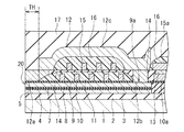
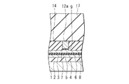
以下、本発明の実施の形態について図面を参照して詳細に説明する。始めに、図3および図4を参照して、本発明の第1の実施の形態に係る薄膜磁気ヘッドの構成および製造方法の概略について説明する。図3は薄膜磁気ヘッドのエアベアリング面および基板に垂直な断面を示す断面図、図4は薄膜磁気ヘッドの磁極部分のエアベアリング面に平行な断面を示す断面図である。
[First Embodiment]
Hereinafter, embodiments of the present invention will be described in detail with reference to the drawings. First, the configuration of the thin film magnetic head and the outline of the manufacturing method according to the first embodiment of the invention will be described with reference to FIGS. FIG. 3 is a cross-sectional view showing a cross section perpendicular to the air bearing surface and the substrate of the thin film magnetic head, and FIG. 4 is a cross sectional view showing a cross section parallel to the air bearing surface of the magnetic pole portion of the thin film magnetic head.
本実施の形態に係る薄膜磁気ヘッドの製造方法では、まず、アルティック(Al2O3・TiC)等のセラミック材料よりなる基板1の上に、スパッタリング法等によって、アルミナ(Al2O3)等の絶縁材料よりなる絶縁層2を、例えば1〜5μmの厚さに形成する。次に、絶縁層2の上に、スパッタリング法またはめっき法等によって、パーマロイ(NiFe)等の磁性材料よりなる再生ヘッド用の下部シールド層3を、例えば約3μmの厚さに形成する。
In the method of manufacturing a thin film magnetic head according to the present embodiment, first, alumina (Al 2 O 3 ) is formed on a
次に、下部シールド層3の上に、スパッタリング法等によって、絶縁材料よりなる下部シールドギャップ膜4を、例えば10〜200nmの厚さに形成する。次に、下部シールドギャップ膜4の上に、再生用のMR素子5と、図示しない一対のバイアス磁界印加層と、一対の電極層6を、それぞれ、例えば数十nmの厚さに形成する。次に、下部シールドギャップ膜4およびMR素子5の上に、スパッタリング法等によって、絶縁材料よりなる上部シールドギャップ膜7を、例えば10〜200nmの厚さに形成する。
Next, the lower
次に、上部シールドギャップ膜7の上に、磁性材料からなり、記録ヘッドの下部磁極層を兼ねた再生ヘッドの上部シールド層8を、例えば3〜4μmの厚さに形成する。なお、上部シールド層8に用いる磁性材料は、NiFe、CoFe、CoFeNi、FeN等の軟磁性材料である。上部シールド層8は、スパッタリング法またはめっき法等によって形成される。なお、上部シールド層8の代わりに、上部シールド層と、この上部シールド層の上にスパッタリング法等によって形成されたアルミナ等の非磁性材料よりなる分離層と、この分離層の上に形成された下部磁極層とを設けてもよい。
Next, the
次に、上部シールド層8の上に、スパッタリング法等によって、アルミナ等の非磁性材料よりなる記録ギャップ層9を、例えば50〜300nmの厚さに形成する。次に、磁路形成のために、後述する薄膜コイルの中心部分において、記録ギャップ層9を部分的にエッチングしてコンタクトホール9aを形成する。
Next, the
次に、記録ギャップ層9の上に、例えば銅(Cu)よりなる薄膜コイルの第1層部分10を、例えば2〜3μmの厚さに形成する。なお、図3において、符号10aは、第1層部分10のうち、後述する薄膜コイルの第2層部分15に接続される接続部を表している。第1層部分10は、コンタクトホール9aの周囲に巻回される。
Next, a
次に、薄膜コイルの第1層部分10およびその周辺の記録ギャップ層9を覆うように、フォトレジスト等の、加熱時に流動性を有する有機絶縁材料よりなる絶縁層11を所定のパターンに形成する。次に、絶縁層11の表面を平坦にするために所定の温度で熱処理する。この熱処理により、絶縁層11の外周および内周の各端縁部分は、丸みを帯びた斜面形状となる。
Next, an insulating
次に、絶縁層11のうちの後述するエアベアリング面20側の斜面部分からエアベアリング面20側にかけての領域において、記録ギャップ層9および絶縁層11の上に、記録ヘッド用の磁性材料によって、上部磁極層12のトラック幅規定層12aを形成する。上部磁極層12は、このトラック幅規定層12aと、後述する連結部分層12bおよびヨーク部分層12cとで構成される。
Next, in a region from the slope portion on the
トラック幅規定層12aは、記録ギャップ層9の上に形成され、上部磁極層12の磁極部分となる先端部と、絶縁層11のエアベアリング面20側の斜面部分の上に形成され、ヨーク部分層12cに接続される接続部とを有している。先端部の幅は記録トラック幅と等しくなっている。接続部の幅は、先端部の幅よりも大きくなっている。
The track
トラック幅規定層12aを形成する際には、同時に、コンタクトホール9aの上に磁性材料よりなる連結部分層12bを形成すると共に、接続部10aの上に磁性材料よりなる接続層13を形成する。連結部分層12bは、上部磁極層12のうち、上部シールド層8に磁気的に連結される部分を構成する。
When the track
次に、磁極トリミングを行う。すなわち、トラック幅規定層12aの周辺領域において、トラック幅規定層12aをマスクとして、記録ギャップ層9および上部シールド層8の磁極部分における記録ギャップ層9側の少なくとも一部をエッチングする。これにより、図4に示したように、上部磁極層12の磁極部分、記録ギャップ層9および上部シールド層8の磁極部分の少なくとも一部の各幅が揃えられたトリム(Trim)構造が形成される。このトリム構造によれば、記録ギャップ層9の近傍における磁束の広がりによる実効的なトラック幅の増加を防止することができる。
Next, magnetic pole trimming is performed. That is, in the peripheral region of the track
次に、全体に、アルミナ等の無機絶縁材料よりなる絶縁層14を、例えば3〜4μmの厚さに形成する。次に、この絶縁層14を、例えば化学機械研磨によって、トラック幅規定層12a、連結部分層12bおよび接続層13の表面に至るまで研磨して平坦化する。
Next, the insulating
次に、平坦化された絶縁層14の上に、例えば銅(Cu)よりなる薄膜コイルの第2層部分15を、例えば2〜3μmの厚さに形成する。なお、図3において、符号15aは、第2層部分15のうち、接続層13を介して薄膜コイルの第1層部分10の接続部10aに接続される接続部を表している。第2層部分15は、連結部分層12bの周囲に巻回される。
Next, a
次に、薄膜コイルの第2層部分15およびその周辺の絶縁層14を覆うように、フォトレジスト等の、加熱時に流動性を有する有機絶縁材料よりなる絶縁層16を所定のパターンに形成する。次に、絶縁層16の表面を平坦にするために所定の温度で熱処理する。この熱処理により、絶縁層16の外周および内周の各端縁部分は、丸みを帯びた斜面形状となる。
Next, an insulating
次に、トラック幅規定層12a、絶縁層14,16および連結部分層12bの上に、パーマロイ等の記録ヘッド用の磁性材料によって、上部磁極層12のヨーク部分を構成するヨーク部分層12cを形成する。ヨーク部分層12cのエアベアリング面20側の端部は、エアベアリング面20から離れた位置に配置されている。また、ヨーク部分層12cは、連結部分層12bを介して上部シールド層8に接続されている。
Next, a
次に、全体を覆うように、例えばアルミナよりなるオーバーコート層17を形成する。最後に、上記各層を含むスライダの機械加工を行って、記録ヘッドおよび再生ヘッドを含む薄膜磁気ヘッドのエアベアリング面20を形成して、薄膜磁気ヘッドが完成する。
Next, an
このようにして製造される薄膜磁気ヘッドは、記録媒体に対向する媒体対向面としてのエアベアリング面20と再生ヘッドと記録ヘッドとを備えている。再生ヘッドは、エアベアリング面20の近傍に配置されたMR素子5と、エアベアリング面20側の一部がMR素子5を挟んで対向するように配置された、MR素子5をシールドするための下部シールド層3および上部シールド層8とを有している。
The thin film magnetic head manufactured in this way includes an
記録ヘッドは、エアベアリング面20側において互いに対向する磁極部分を含むと共に、互いに磁気的に連結された下部磁極層(上部シールド層8)および上部磁極層12と、この下部磁極層の磁極部分と上部磁極層12の磁極部分との間に設けられた記録ギャップ層9と、少なくとも一部が下部磁極層および上部磁極層12の間に、これらに対して絶縁された状態で配設された薄膜コイル10,15とを有している。この薄膜磁気ヘッドでは、図3に示したように、エアベアリング面20から、絶縁層11のエアベアリング面20側の端部までの長さが、スロートハイトTHとなる。なお、スロートハイトとは、エアベアリング面20から、2つの磁極層の間隔が開き始める位置までの長さ(高さ)をいう。
The recording head includes magnetic pole portions that face each other on the
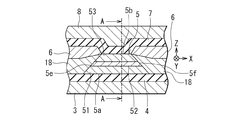
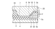
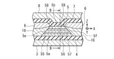
次に、図1および図2を参照して、本実施の形態における再生ヘッドの構成について詳しく説明する。図1は、再生ヘッドのエアベアリング面に平行な断面を示す断面図である。図2は、図1のA−A線断面図である。図1および図2では、トラック幅方向、すなわちエアベアリング面20に平行で且つMR素子5の面5a,5bに平行な方向をX方向とし、エアベアリング面20に垂直な方向をY方向とし、X方向およびY方向に垂直な方向をZ方向としている。
Next, with reference to FIG. 1 and FIG. 2, the structure of the reproducing head in the present embodiment will be described in detail. FIG. 1 is a cross-sectional view showing a cross section parallel to the air bearing surface of the read head. 2 is a cross-sectional view taken along line AA in FIG. 1 and 2, the track width direction, that is, the direction parallel to the
再生ヘッドは、所定の間隔を開けて配置された下部シールド層3および上部シールド層8と、この下部シールド層3と上部シールド層8との間に配置されたMR素子5と、下部シールド層3とMR素子5との間に配置された下部シールドギャップ膜4と、上部シールド層8とMR素子5との間に配置された上部シールドギャップ膜7とを備えている。なお、MR素子5が配置された領域およびその周辺の一部の領域を除いて、上部シールドギャップ膜7と上部シールド層8との間には、アルミナ等の絶縁材料よりなる絶縁層19が形成されている。
The reproducing head includes a
MR素子5は、互いに反対側を向き且つエアベアリング面20と交差するように配置された第1の面(下面)5aおよび第2の面(上面)5bと、エアベアリング面20に配置された端部5cと、端部5cとは反対側の端部5dと、2つの側部5e,5fとを有している。下部シールドギャップ膜4はMR素子5の第1の面5aに隣接するように配置され、上部シールドギャップ膜7はMR素子5の第2の面5bに隣接するように配置されている。下部シールドギャップ膜4と上部シールドギャップ膜7は、本発明における絶縁膜に対応する。
The
端部5dは、端部5c,5d間の距離がMR素子5の上側ほど小さくなるように傾斜している。また、側部5e,5fも、側部5e,5f間の距離がMR素子5の上側ほど小さくなるように傾斜している。
The
再生ヘッドは、更に、MR素子5の各側部5e,5fに隣接するように配置され、MR素子5に対してバイアス磁界を印加する2つのバイアス磁界印加層18と、それぞれ各バイアス磁界印加層18の上面に隣接するように配置され、MR素子5に対して信号検出用の電流であるセンス電流を流す2つの電極層6とを備えている。図1では、電極層6はバイアス磁界印加層18の上に配置されているが、バイアス磁界印加層18のない領域では、電極層6は下部シールドギャップ膜4の上に配置されている。バイアス磁界印加層18および電極層6は、下部シールドギャップ膜4と上部シールドギャップ膜7との間に配置されている。
The reproducing head is further disposed adjacent to the
バイアス磁界印加層18は、硬磁性層(ハードマグネット)や、強磁性層と反強磁性層との積層体等を用いて構成される。電極層6は、例えば、Ta層とAu層との積層体、Tiw層とTa層の積層体、あるいはTiN層とTa層の積層体等によって構成される。
The bias magnetic
バイアス磁界印加層18は、バイアス磁界印加層18の磁化がトラック幅方向に向くように着磁され、MR素子5に対してトラック幅方向のバイアス磁界を印加する。
The bias magnetic
MR素子5は、互いに反対側を向く2つの面を有する非磁性導電層52と、この非磁性導電層52における一方の面に隣接するように配置され、外部磁界に応じて磁化の方向が変化するフリー層53と、非磁性導電層52の他方の面に隣接するように配置され、エアベアリング面20に垂直な方向に磁化の方向が固定された固定層51とを含んでいる。しかし、MR素子5は、固定層51の磁化の方向を固定するための、反強磁性層のような他の層を含んでいない。固定層51は、反強磁性層のような他の層の作用によらずに磁化の方向が固定されている。なお、図1は、フリー層53が非磁性導電層52の上に配置され、固定層51が非磁性導電層52の下に配置された例を示している。しかし、フリー層53が非磁性導電層52の下に配置され、固定層51が非磁性導電層52の上に配置されていてもよい。
The
MR素子5は、各層51,52,53となる膜を順に形成した後、これらの積層体をパターニングすることによって形成される。積層体のパターニングは、例えば、積層体の上に、フォトリソグラフィによってマスクを形成し、このマスクを用いて、イオンミリング等のドライエッチングによって、積層体を選択的にエッチングすることによって行なわれる。このエッチングによって、傾斜した端部5dおよび側部5e,5fが形成される。
The
非磁性導電層52は、Cu、Au、Ag等の非磁性の導電性材料によって構成されている。フリー層53は、1つ以上の軟磁性層を含んでいる。
The nonmagnetic
固定層51は、例えば、2つの強磁性層と、これらの間に配置された薄い結合層とを有している。この場合、2つの強磁性層は、反強磁性的に、すなわち、それぞれの磁化の方向が反平行になるように結合する。結合層は、Ru、Rh、Ir、Re、Cr、Zr等の非磁性材料によって構成されている。固定層51は、このような3層構造のものに限らず、保磁力の大きな1つの強磁性層によって構成されていてもよい。本実施の形態において、固定層51に含まれる強磁性層は、磁歪定数が正の値の強磁性材料によって構成されている。この強磁性材料は、金属でもよいし合金でもよい。磁歪定数が正の値の強磁性材料としては、例えば、FeCo(Fe:70重量%,Co:30重量%)や、SmCoがある。
The fixed
固定層51は、着磁されることによって誘導磁気異方性が与えられており、その磁化の方向がエアベアリング面20に垂直な方向に固定されている。
The fixed
また、本実施の形態において、下部シールドギャップ膜4と上部シールドギャップ膜7は、いずれも、600MPa以上の圧縮応力を有している。ただし、膜4,7の圧縮応力が大き過ぎると、それらに接する層に対する密着性が低下するため、膜4,7の圧縮応力は、4000MPa以下であることが好ましい。
In the present embodiment, both the lower
下部シールドギャップ膜4および上部シールドギャップ膜7の材料は、SiO2、SiC、SiN、AlN、TiO、BNのいずれかを含んでいてもよい。また、下部シールドギャップ膜4および上部シールドギャップ膜7は、多層膜で構成されていてもよい。
The material of the lower
下部シールドギャップ膜4および上部シールドギャップ膜7は、例えばスパッタリング法によって形成される。スパッタリング法によって形成される絶縁膜には、圧縮応力が残留する場合が多い。しかし、この圧縮応力の大きさは、絶縁膜の材料および成膜条件によって異なる。そのため、600MPa以上の圧縮応力を有する膜4,7を形成するためには、膜4,7の材料の選定と共に、膜4,7の成膜条件の選定が必要である。膜4,7の材料は、SiO2、SiC、SiN、AlN、TiO、BNのいずれかを含んでいてもよい。これらの材料を用いることにより、成膜条件にも依るが、600MPa以上の圧縮応力を有する膜4,7を形成することが可能となる。スパッタリング法によって膜4,7を形成する場合には、使用する複数のガスの流量比、ガスの圧力、ターゲットに供給される電力、基板に供給される電力等の成膜条件が、膜4,7の残留応力に影響を与える。従って、膜4,7の圧縮応力が600MPa以上となるように、これらの成膜条件の1つ以上を制御する必要がある。
The lower
次に、本実施の形態に係る薄膜磁気ヘッドの作用について説明する。薄膜磁気ヘッドは、記録ヘッドによって記録媒体に情報を記録し、再生ヘッドによって、記録媒体に記録されている情報を再生する。 Next, the operation of the thin film magnetic head according to the present embodiment will be described. The thin film magnetic head records information on a recording medium with a recording head, and reproduces information recorded on the recording medium with a reproducing head.
再生ヘッドにおいて、フリー層53に外部磁界が印加されない状態では、フリー層53の磁化は、バイアス磁界印加層18からのバイアス磁界によって、トラック幅方向Xに向けられている。一方、固定層51の磁化の方向は、エアベアリング面20に垂直な方向Yに固定されている。従って、フリー層53に記録媒体からの信号磁界が印加されない状態では、固定層51の磁化の方向とフリー層53の磁化の方向とがなす角度は90°に保たれる。この再生ヘッドに、記録媒体から、エアベアリング面20に垂直な方向の信号磁界が印加されると、フリー層53の磁化の方向が変化し、その結果、固定層51の磁化の方向とフリー層53の磁化の方向とがなす角度が変化する。この角度によってMR素子5の電気抵抗が変化する。従って、このMR素子5の電気抵抗の変化を検出することにより、記録媒体に記録された情報を再生することができる。MR素子5の電気抵抗は、MR素子5にセンス電流を流したときの2つの電極層6間の電位差より求めることができる。
In the reproducing head, when no external magnetic field is applied to the
本実施の形態において、固定層51は、磁歪定数が正の値の強磁性材料よりなる層を含んでいる。また、MR素子5の第1の面5aに隣接する下部シールドギャップ膜4およびMR素子5の第2の面5bに隣接する上部シールドギャップ膜7は、いずれも600MPa以上の圧縮応力を有している。そのため、固定層51には大きな引っ張り応力が与えられる。これにより、磁歪定数が正の値の強磁性材料よりなる層を含む固定層51において、逆磁歪効果により、磁化をエアベアリング面20に垂直な方向に向ける磁気異方性が大きくなり、固定層51の磁化の方向が強固に固定される。このように、本実施の形態に係る薄膜磁気ヘッドによれば、他の層の作用によらずに磁化の方向が固定された固定層51を含むスピンバルブ型のMR素子5を用いながら、固定層51の磁化の方向を強固に固定することができる。
In the present embodiment, the fixed
次に、本実施の形態の効果を確認するために行なった実験の結果について説明する。この実験では、第1および第2の実施例の再生ヘッドと比較例の再生ヘッドとを作製した。いずれの再生ヘッドも、図1および図2に示した構造を有している。 Next, the results of experiments conducted to confirm the effects of this embodiment will be described. In this experiment, the reproducing heads of the first and second examples and the reproducing head of the comparative example were produced. Each reproducing head has the structure shown in FIGS.
第1の実施例の再生ヘッドでは、下部シールドギャップ膜4および上部シールドギャップ膜7を、材料としてSiO2を用いて、以下の方法によって形成した。成膜方法は、電子サイクロトロン共鳴(Electron Cyclotron Resonance;以下、ECRと記す。)スパッタリング法を用いた。ターゲット材は、Siとした。ガスは、ArとO2の混合ガスとした。ガスの流量は、Arについては20sccm、O2については5sccmとした。混合ガスの圧力は8×10⁻²Paとした。マイクロ波電力は500Wとし、ターゲットに与えられる電力は500Wとした。
In the reproducing head of the first example, the lower
第2の実施例の再生ヘッドでは、下部シールドギャップ膜4および上部シールドギャップ膜7を、材料としてSiO2を用いて、以下の方法によって形成した。成膜方法は、ECRスパッタリング法を用いた。ターゲット材は、Siとした。ガスは、ArとO2の混合ガスとした。ガスの流量は、Arについては20sccm、O2については10sccmとした。混合ガスの圧力は1.0×10⁻¹Paとした。マイクロ波電力は500Wとし、ターゲットに与えられる電力は500Wとした。
In the reproducing head of the second example, the lower
比較例の再生ヘッドでは、下部シールドギャップ膜4および上部シールドギャップ膜7を、材料としてアルミナ(Al2O3)を用いて、以下の方法によって形成した。成膜方法は、ECRスパッタリング法を用いた。ターゲット材は、Alとした。ガスは、ArとO2の混合ガスとした。ガスの流量は、Arについては20sccm、O2については5sccmとした。混合ガスの圧力は8×10⁻²Paとした。マイクロ波電力は500Wとし、ターゲットに与えられる電力は500Wとした。
In the reproducing head of the comparative example, the lower
第1の実施例の再生ヘッドにおける膜4,7の内部応力は、600MPaの圧縮応力であった。第2の実施例の再生ヘッドにおける膜4,7の内部応力は、900MPaの圧縮2応力であった。一方、比較例の再生ヘッドにおける膜4,7の内部応力は、300MPaの圧縮応力であった。
The internal stress of the
第1および第2の実施例の再生ヘッドと比較例の再生ヘッドは、それぞれ1枚のウェハを用いて、以下のように同時に多数作製した。すなわち、まず、ウェハ上に複数列に配列されるように再生ヘッドを形成した。ただし、この時点では、固定層51の着磁とバイアス磁界印加層18の着磁は行なわれていない。次に、ウェハを切断して、複数の再生ヘッドが一列に配列されたバー状のブロックを形成した。このブロックの1つの面には、複数の再生ヘッドのエアベアリング面20となる面が現れている。次に、このブロックにおける上記の面を研磨して、複数の再生ヘッドのエアベアリング面20を形成した。次に、このブロックの状態で、固定層51に、エアベアリング面20に垂直な方向の5kOe(5×79.6kA/m)の磁界を印加して、固定層51の着磁を行なった。この着磁により、固定層51の磁化はエアベアリング面20に垂直な方向に向けられた。次に、バイアス磁界印加層18に、トラック幅方向の1.5kOe(1.5×79.6kA/m)の磁界を印加して、バイアス磁界印加層18の着磁を行なった。この着磁により、バイアス磁界印加層18の磁化はトラック幅方向に向けられた。以上のようにして、第1の実施例の再生ヘッド、第2の実施例の再生ヘッドおよび比較例の再生ヘッドを、100個ずつ作製した。
The reproducing heads of the first and second examples and the reproducing head of the comparative example were each manufactured in large numbers at the same time using one wafer each as follows. That is, first, reproducing heads were formed so as to be arranged in a plurality of rows on the wafer. However, at this time, the magnetization of the fixed
実験では、100個の第1の実施例の再生ヘッド、100個の第2の実施例の再生ヘッドおよび100個の比較例の再生ヘッドについて、以下のような測定を行なって、固定層51の磁化方向の固定の強さを調べた。この測定では、まず、ブロックに含まれる各再生ヘッドに対して、擬似静的試験(Quasi static test)を行なって、再生ヘッドの出力を調べた。この試験は、再生ヘッドに対して、エアベアリング面20に垂直な方向に、−200Oe〜200Oe(−200×79.6A/m〜200×79.6A/m)の交番外部磁界を印加して行なった。次に、各再生ヘッドに対して、トラック幅方向に1.7kOe(1.7×79.6kA/m)の外乱磁界を印加し、その後、外乱磁界の印加を解除してから、前述と同様の擬似静的試験を行なって、再生ヘッドの出力を調べた。以下、外乱磁界の大きさを0.2kOe(0.2×79.6kA/m)ずつ大きくしながら、外乱磁界の大きさが4.1kOe(4.1×79.6kA/m)に達するまで、同様の試験を繰り返し行なった。
In the experiment, the following measurements were performed on 100 reproduction heads of the first embodiment, 100 reproduction heads of the second embodiment, and 100 reproduction heads of the comparative example, and the fixed
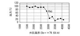
実験では、出力が所望の値に対して10%以上低下した再生ヘッドを不良とみなした。なお、実験では、所望の値を1000μVとした。図9は、1つの再生ヘッドにおける外乱磁界と出力との関係の一例を示している。図9において、横軸は外乱磁界を表し、縦軸は、所望の出力を100%としたときの再生ヘッドの出力(%)を表している。この例における再生ヘッドでは、作製後、最初の試験における出力は100%であった。この例では、外乱磁界を大きくしていき、外乱磁界が2.9kOe(2.9×79.6kA/m)に達したときに、出力が所望の値に対して10%以上低下している。このとき、固定層51の磁化の方向は、エアベアリング面20に垂直な方向に対して傾いていると考えられる。実験では、このように、外乱磁界を大きくしていき、初めて、出力が所望の値に対して10%以上低下したときの外乱磁界を、不良発生磁界HNGと定義した。
In the experiment, a read head whose output decreased by 10% or more with respect to a desired value was regarded as defective. In the experiment, a desired value was set to 1000 μV. FIG. 9 shows an example of the relationship between the disturbance magnetic field and the output in one reproducing head. In FIG. 9, the horizontal axis represents the disturbance magnetic field, and the vertical axis represents the output (%) of the reproducing head when the desired output is 100%. In the reproducing head in this example, the output in the first test after production was 100%. In this example, when the disturbance magnetic field is increased and the disturbance magnetic field reaches 2.9 kOe (2.9 × 79.6 kA / m), the output is reduced by 10% or more with respect to a desired value. . At this time, it is considered that the magnetization direction of the fixed
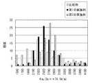
図10は、100個の第1の実施例の再生ヘッド、100個の第2の実施例の再生ヘッドおよび100個の比較例の再生ヘッドについて、不良発生磁界HNGの分布を調べた結果を示している。図10において、横軸は不良発生磁界HNGを表し、縦軸は再生ヘッドの個数を表している。なお、図10に示した結果によると、不良発生磁界HNGが1.5kOe(1.5×79.6kA/m)である再生ヘッドも存在している。この再生ヘッドは、作製後、最初の試験で10%以上の出力低下が認められた再生ヘッドである。 FIG. 10 shows the result of examining the distribution of the defective magnetic field H NG for 100 reproducing heads of the first embodiment, 100 reproducing heads of the second embodiment, and 100 reproducing heads of the comparative example. Show. In FIG. 10, the horizontal axis represents the defect occurrence magnetic field H NG and the vertical axis represents the number of reproducing heads. According to the result shown in FIG. 10, there is also a read head having a defective magnetic field H NG of 1.5 kOe (1.5 × 79.6 kA / m). This read head is a read head in which an output drop of 10% or more was recognized in the first test after production.
図10に示した結果より、以下のことが分かる。まず、100個の比較例の再生ヘッドにおいては、不良発生磁界HNGが2.3kOe(2.3×79.6kA/m)となる再生ヘッドが最も多く、17個存在している。また、比較例の再生ヘッドにおいては、不良発生磁界HNGが1.5kOe(1.5×79.6kA/m)〜3.1kOe(3.1×79.6kA/m)の範囲内となる再生ヘッドが84個存在している。このことから、比較例の再生ヘッドでは、不良発生磁界HNGのばらつきが大きいことが分かる。更に、比較例の再生ヘッドでは、不良発生磁界HNGが1.5kOe(1.5×79.6kA/m)となる再生ヘッドが7個存在している。この7個の再生ヘッドは、バイアス磁界印加層18の着磁によって、固定層51の磁化の方向がエアベアリング面20に垂直な方向に対して傾いて、不良となったものである。
From the results shown in FIG. 10, the following can be understood. First, in the 100 reproducing heads of the comparative example, the number of reproducing heads having a defect generation magnetic field H NG of 2.3 kOe (2.3 × 79.6 kA / m) is the largest, and there are 17 reproducing heads. In the reproducing head of the comparative example, the defect generation magnetic field H NG is in the range of 1.5 kOe (1.5 × 79.6 kA / m) to 3.1 kOe (3.1 × 79.6 kA / m). There are 84 playback heads. From this, it can be seen that in the reproducing head of the comparative example, the variation of the defect occurrence magnetic field H NG is large. Further, in the reproducing head of the comparative example, there are seven reproducing heads having a defect occurrence magnetic field H NG of 1.5 kOe (1.5 × 79.6 kA / m). The seven reproducing heads are defective because the magnetization direction of the fixed
一方、100個の第1の実施例の再生ヘッドにおいては、不良発生磁界HNGが2.5kOe(2.5×79.6kA/m)となる再生ヘッドが最も多く、26個存在している。また、第1の実施例の再生ヘッドにおいては、不良発生磁界HNGが2.1kOe(2.1×79.6kA/m)〜2.9kOe(2.9×79.6kA/m)の範囲内となる再生ヘッドが82個存在している。このことから、第1の実施例の再生ヘッドでは、比較例の再生ヘッドに比べて、不良発生磁界HNGのばらつきが小さく、且つ不良発生磁界HNGの分布が不良発生磁界HNGの大きい方へ移動していることが分かる。更に、第1の実施例の再生ヘッドでは、不良発生磁界HNGが1.5kOe(1.5×79.6kA/m)となる再生ヘッドは1個しか存在していない。 On the other hand, in the 100 reproducing heads of the first embodiment, there are the largest number of reproducing heads with a defect occurrence magnetic field H NG of 2.5 kOe (2.5 × 79.6 kA / m), and there are 26 reproducing heads. . In the reproducing head of the first embodiment, the defect generation magnetic field H NG ranges from 2.1 kOe (2.1 × 79.6 kA / m) to 2.9 kOe (2.9 × 79.6 kA / m). There are 82 playback heads inside. Therefore, the reproducing head in the first embodiment, as compared with the reproducing head of the comparative example, small variations in the failure field H NG, and larger defects generated magnetic field H NG distributions failure field H NG You can see that it has moved to. Further, in the reproducing head of the first embodiment, there is only one reproducing head having a defective magnetic field H NG of 1.5 kOe (1.5 × 79.6 kA / m).
また、100個の第2の実施例の再生ヘッドにおいては、不良発生磁界HNGが2.7kOe(2.7×79.6kA/m)となる再生ヘッドが最も多く、28個存在している。また、第2の実施例の再生ヘッドにおいては、不良発生磁界HNGが2.3kOe(2.3×79.6kA/m)〜3.1kOe(3.1×79.6kA/m)の範囲内となる再生ヘッドが83個存在している。このことから、第2の実施例の再生ヘッドでは、比較例の再生ヘッドに比べて、不良発生磁界HNGのばらつきが小さく、且つ不良発生磁界HNGの分布が不良発生磁界HNGの大きい方へ移動していることが分かる。更に、第2の実施例の再生ヘッドでは、不良発生磁界HNGが1.5kOe(1.5×79.6kA/m)となる再生ヘッドは存在していない。 In the 100 reproducing heads of the second embodiment, there are the largest number of reproducing heads with a defective magnetic field H NG of 2.7 kOe (2.7 × 79.6 kA / m), and there are 28 reproducing heads. . Further, in the reproducing head of the second embodiment, the defect generation magnetic field H NG is in the range of 2.3 kOe (2.3 × 79.6 kA / m) to 3.1 kOe (3.1 × 79.6 kA / m). There are 83 playback heads inside. Therefore, the reproducing head of the second embodiment, as compared with the reproducing head of the comparative example, small variations in the failure field H NG, and larger defects generated magnetic field H NG distributions failure field H NG You can see that it has moved to. Further, in the reproducing head of the second embodiment, there is no reproducing head having a defect generation magnetic field H NG of 1.5 kOe (1.5 × 79.6 kA / m).
これらのことから、第1および第2の実施例の再生ヘッドは比較例の再生ヘッドに比べて、固定層51の磁化の方向が強固に固定されていることが分かる。また、このことから、膜4,7における圧縮応力を大きくすることにより、固定層51の磁化の方向を強固に固定できることが分かる。
From these facts, it can be seen that the direction of magnetization of the fixed
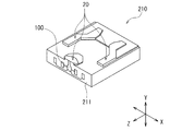
以下、本実施の形態に係るヘッドジンバルアセンブリおよびハードディスク装置について説明する。まず、図5を参照して、ヘッドジンバルアセンブリに含まれるスライダ210について説明する。ハードディスク装置において、スライダ210は、回転駆動される円盤状の記録媒体であるハードディスクに対向するように配置される。このスライダ210は、主に図3における基板1およびオーバーコート層17からなる基体211を備えている。基体211は、ほぼ六面体形状をなしている。基体211の六面のうちの一面は、ハードディスクに対向するようになっている。この一面には、エアベアリング面20が形成されている。ハードディスクが図5におけるZ方向に回転すると、ハードディスクとスライダ210との間を通過する空気流によって、スライダ210に、図5におけるY方向の下方に揚力が生じる。スライダ210は、この揚力によってハードディスクの表面から浮上するようになっている。なお、図5におけるX方向は、ハードディスクのトラック横断方向である。スライダ210の空気流出側の端部(図5における左下の端部)の近傍には、本実施の形態に係る薄膜磁気ヘッド100が形成されている。
Hereinafter, the head gimbal assembly and the hard disk device according to the present embodiment will be described. First, the
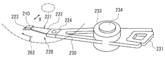
次に、図6を参照して、本実施の形態に係るヘッドジンバルアセンブリ220について説明する。ヘッドジンバルアセンブリ220は、スライダ210と、このスライダ210を弾性的に支持するサスペンション221とを備えている。サスペンション221は、例えばステンレス鋼によって形成された板ばね状のロードビーム222、このロードビーム222の一端部に設けられると共にスライダ210が接合され、スライダ210に適度な自由度を与えるフレクシャ223と、ロードビーム222の他端部に設けられたベースプレート224とを有している。ベースプレート224は、スライダ210をハードディスク262のトラック横断方向Xに移動させるためのアクチュエータのアーム230に取り付けられるようになっている。アクチュエータは、アーム230と、このアーム230を駆動するボイスコイルモータとを有している。フレクシャ223において、スライダ210が取り付けられる部分には、スライダ210の姿勢を一定に保つためのジンバル部が設けられている。
Next, the
ヘッドジンバルアセンブリ220は、アクチュエータのアーム230に取り付けられる。1つのアーム230にヘッドジンバルアセンブリ220を取り付けたものはヘッドアームアセンブリと呼ばれる。また、複数のアームを有するキャリッジの各アームにヘッドジンバルアセンブリ220を取り付けたものはヘッドスタックアセンブリと呼ばれる。
The
図6は、ヘッドアームアセンブリの一例を示している。このヘッドアームアセンブリでは、アーム230の一端部にヘッドジンバルアセンブリ220が取り付けられている。アーム230の他端部には、ボイスコイルモータの一部となるコイル231が取り付けられている。アーム230の中間部には、アーム230を回動自在に支持するための軸234に取り付けられる軸受け部233が設けられている。
FIG. 6 shows an example of the head arm assembly. In this head arm assembly, a
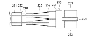
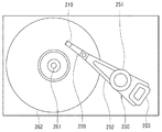
次に、図7および図8を参照して、ヘッドスタックアセンブリの一例と本実施の形態に係るハードディスク装置について説明する。図7はハードディスク装置の要部を示す説明図、図8はハードディスク装置の平面図である。ヘッドスタックアセンブリ250は、複数のアーム252を有するキャリッジ251を有している。複数のアーム252には、複数のヘッドジンバルアセンブリ220が、互いに間隔を開けて垂直方向に並ぶように取り付けられている。キャリッジ251においてアーム252とは反対側には、ボイスコイルモータの一部となるコイル253が取り付けられている。ヘッドスタックアセンブリ250は、ハードディスク装置に組み込まれる。ハードディスク装置は、スピンドルモータ261に取り付けられた複数枚のハードディスク262を有している。各ハードディスク262毎に、ハードディスク262を挟んで対向するように2つのスライダ210が配置される。また、ボイスコイルモータは、ヘッドスタックアセンブリ250のコイル253を挟んで対向する位置に配置された永久磁石263を有している。
Next, an example of the head stack assembly and the hard disk device according to the present embodiment will be described with reference to FIGS. FIG. 7 is an explanatory view showing a main part of the hard disk device, and FIG. 8 is a plan view of the hard disk device. The
スライダ210を除くヘッドスタックアセンブリ250およびアクチュエータは、本発明における位置決め装置に対応し、スライダ210を支持すると共にハードディスク262に対して位置決めする。
The
本実施の形態に係るハードディスク装置では、アクチュエータによって、スライダ210をハードディスク262のトラック横断方向に移動させて、スライダ210をハードディスク262に対して位置決めする。スライダ210に含まれる薄膜磁気ヘッドは、記録ヘッドによって、ハードディスク262に情報を記録し、再生ヘッドによって、ハードディスク262に記録されている情報を再生する。
In the hard disk device according to the present embodiment, the
本実施の形態に係るヘッドジンバルアセンブリおよびハードディスク装置は、前述の本実施の形態に係る薄膜磁気ヘッドと同様の効果を奏する。 The head gimbal assembly and hard disk device according to the present embodiment have the same effects as those of the thin film magnetic head according to the present embodiment described above.
[第2の実施の形態]
次に、図11および図12を参照して、本発明の第2の実施の形態について説明する。図11は、本実施の形態における再生ヘッドのエアベアリング面に平行な断面を示す断面図である。図12は、図11のB−B線断面図である。
[Second Embodiment]
Next, a second embodiment of the present invention will be described with reference to FIG. 11 and FIG. FIG. 11 is a cross-sectional view showing a cross section parallel to the air bearing surface of the read head in the present embodiment. 12 is a cross-sectional view taken along line BB in FIG.
本実施の形態では、MR素子5の構成が、第1の実施の形態とは異なり、いわゆるデュアルスピンバルブ型のGMR素子の構成となっている。本実施の形態では、MR素子5は、フリー層57と、第1の非磁性導電層56、第2の非磁性導電層58と、第1の固定層55および第2の固定層59とを含んでいる。しかし、第1の実施の形態と同様に、MR素子5は、固定層55,59の磁化の方向を固定するための、反強磁性層のような他の層を含んでいない。固定層55,59は、反強磁性層のような他の層の作用によらずに磁化の方向が固定されている。
In the present embodiment, the configuration of the
フリー層57は、互いに反対側を向く2つの面を有している。第1の非磁性導電層56は、互いに反対側を向く2つの面を有し、一方の面(上面)がフリー層57における一方の面(下面)に隣接するように配置されている。第2の非磁性導電層58は、互いに反対側を向く2つの面を有し、一方の面(下面)がフリー層57における他方の面(上面)に隣接するように配置されている。第1の固定層55は、第1の非磁性導電層56の他方の面(下面)に隣接するように配置されている。第2の固定層59は、第2の非磁性導電層58の他方の面(上面)に隣接するように配置されている。
The
フリー層57、非磁性導電層56,58、固定層55,59の材料や機能は、それぞれ、第1の実施の形態におけるフリー層53、非磁性導電層52、固定層51と同様である。また、MR素子5の作用も第1の実施の形態と同様である。本実施の形態によれば、第1の実施の形態に比べて、MR素子5の抵抗変化率を大きくすることが可能である。
The materials and functions of the
本実施の形態におけるその他の構成、作用および効果は、第1の実施の形態と同様である。 Other configurations, operations, and effects in the present embodiment are the same as those in the first embodiment.
なお、本発明は、上記各実施の形態に限定されず、種々の変更が可能である。例えば、実施の形態では、下部シールドギャップ膜4と上部シールドギャップ膜7の両方が600MPa以上の圧縮応力を有するようにしたが、膜4,7のいずれか一方のみが600MPa以上の圧縮応力を有するようにしてもよい。この場合にも、固定層に大きな引っ張り応力を与えることができ、これにより、固定層の磁化の方向を強固に固定することができる。
In addition, this invention is not limited to said each embodiment, A various change is possible. For example, in the embodiment, both the lower
また、MR素子5は、デュアルスピンバルブ型のGMR素子であって、2つの固定層のうちの一方は、反強磁性層のような他の層の作用によらずに磁化の方向が固定され、2つの固定層のうちの他方は、反強磁性層のような他の層の作用によって磁化の方向が固定されたものであってもよい。
The
また、実施の形態では、基体側に再生ヘッドを形成し、その上に、記録ヘッドを積層した構造の薄膜磁気ヘッドについて説明したが、この積層順序を逆にしてもよい。 In the embodiment, a thin film magnetic head having a structure in which a reproducing head is formed on the substrate side and a recording head is stacked thereon has been described. However, the stacking order may be reversed.
また、読み取り専用として用いる場合には、薄膜磁気ヘッドを、再生ヘッドだけを備えた構成としてもよい。 When used as a read-only device, the thin film magnetic head may be configured to include only the reproducing head.
1…基板、2…絶縁層、3…下部シールド層、4…下部シールドギャップ膜、5…MR素子、6…電極層、7…上部シールドギャップ膜、8…上部シールド層、9…記録ギャップ層、10…薄膜コイルの第1層部分、12…上部磁極層、15…薄膜コイルの第2層部分、17…オーバーコート層、18…バイアス磁界印加層、20…エアベアリング面、51…固定層、52…非磁性導電層、53…フリー層。
DESCRIPTION OF
Claims (6)
互いに反対側を向き且つ前記媒体対向面と交差するように配置された第1および第2の面を有し、前記媒体対向面の近傍に配置された磁気抵抗効果素子と、
前記磁気抵抗効果素子の第1の面または第2の面に隣接するように配置された絶縁膜とを備えた薄膜磁気ヘッドであって、
前記磁気抵抗効果素子は、互いに反対側を向く2つの面を有する非磁性導電層と、前記非磁性導電層における一方の面に隣接するように配置され、外部磁界に応じて磁化の方向が変化するフリー層と、前記非磁性導電層の他方の面に隣接するように配置され、他の層の作用によらずに前記媒体対向面に垂直な方向に磁化の方向が固定された固定層とを含み、
前記固定層は、磁歪定数が正の値の強磁性材料よりなる層を含み、
前記絶縁膜は、600MPa以上の圧縮応力を有することを特徴とする薄膜磁気ヘッド。 A medium facing surface facing the recording medium;
A magnetoresistive element having first and second surfaces arranged opposite to each other and intersecting the medium facing surface, and disposed in the vicinity of the medium facing surface;
A thin film magnetic head comprising an insulating film disposed adjacent to the first surface or the second surface of the magnetoresistive element;
The magnetoresistive element is disposed adjacent to one surface of the nonmagnetic conductive layer having two surfaces facing opposite to each other and the nonmagnetic conductive layer, and the direction of magnetization changes according to an external magnetic field. A free layer that is disposed adjacent to the other surface of the nonmagnetic conductive layer, and a pinned layer whose magnetization direction is fixed in a direction perpendicular to the medium facing surface without the action of the other layer; Including
The fixed layer includes a layer made of a ferromagnetic material having a positive magnetostriction constant,
The thin film magnetic head, wherein the insulating film has a compressive stress of 600 MPa or more.
前記フリー層は、互いに反対側を向く2つの面を有し、
前記第1の非磁性導電層は、互いに反対側を向く2つの面を有し、一方の面が前記フリー層における一方の面に隣接するように配置され、
前記第2の非磁性導電層は、互いに反対側を向く2つの面を有し、一方の面が前記フリー層における他方の面に隣接するように配置され、
前記第1の固定層は、前記第1の非磁性導電層の他方の面に隣接するように配置され、
前記第2の固定層は、前記第2の非磁性導電層の他方の面に隣接するように配置され、
前記第1および第2の固定層の少なくとも一方は、他の層の作用によらずに前記媒体対向面に垂直な方向に磁化の方向が固定された固定層であることを特徴とする請求項1ないし3のいずれかに記載の薄膜磁気ヘッド。 The magnetoresistive element includes the free layer, first and second nonmagnetic conductive layers as the nonmagnetic conductive layer, and first and second pinned layers,
The free layer has two surfaces facing away from each other;
The first nonmagnetic conductive layer has two surfaces facing away from each other, and is disposed so that one surface is adjacent to one surface of the free layer,
The second nonmagnetic conductive layer has two surfaces facing away from each other, and is disposed so that one surface is adjacent to the other surface of the free layer,
The first pinned layer is disposed adjacent to the other surface of the first nonmagnetic conductive layer,
The second pinned layer is disposed adjacent to the other surface of the second nonmagnetic conductive layer,
The at least one of the first and second pinned layers is a pinned layer whose magnetization direction is fixed in a direction perpendicular to the medium facing surface regardless of the action of other layers. The thin film magnetic head according to any one of 1 to 3.
前記スライダを弾性的に支持するサスペンションと
を備えたことを特徴とするヘッドジンバルアセンブリ。 A slider comprising the thin film magnetic head according to claim 1, wherein the slider is disposed so as to face a recording medium;
A head gimbal assembly comprising a suspension for elastically supporting the slider.
前記スライダを支持すると共に前記記録媒体に対して位置決めする位置決め装置と
を備えたことを特徴とするハードディスク装置。
A slider that includes the thin film magnetic head according to claim 1 and that is disposed so as to face a disk-shaped recording medium that is rotationally driven;
A hard disk device comprising: a positioning device that supports the slider and positions the slider relative to the recording medium.
Priority Applications (2)
| Application Number | Priority Date | Filing Date | Title |
|---|---|---|---|
| JP2004109712A JP2005293761A (en) | 2004-04-02 | 2004-04-02 | Thin film magnetic head, head gimbal assembly, and hard disk drive unit |
| US11/078,580 US7948718B2 (en) | 2004-04-02 | 2005-03-14 | Magnetoresistive head having an insulating layer with a particular compressive stress |
Applications Claiming Priority (1)
| Application Number | Priority Date | Filing Date | Title |
|---|---|---|---|
| JP2004109712A JP2005293761A (en) | 2004-04-02 | 2004-04-02 | Thin film magnetic head, head gimbal assembly, and hard disk drive unit |
Publications (1)
| Publication Number | Publication Date |
|---|---|
| JP2005293761A true JP2005293761A (en) | 2005-10-20 |
Family
ID=35054022
Family Applications (1)
| Application Number | Title | Priority Date | Filing Date |
|---|---|---|---|
| JP2004109712A Pending JP2005293761A (en) | 2004-04-02 | 2004-04-02 | Thin film magnetic head, head gimbal assembly, and hard disk drive unit |
Country Status (2)
| Country | Link |
|---|---|
| US (1) | US7948718B2 (en) |
| JP (1) | JP2005293761A (en) |
Families Citing this family (6)
| Publication number | Priority date | Publication date | Assignee | Title |
|---|---|---|---|---|
| US8867176B1 (en) * | 2006-06-06 | 2014-10-21 | Oracle America, Inc. | Corrosion protection utilizing a milled, top spin valve GMR sensor |
| US8922955B1 (en) * | 2006-06-06 | 2014-12-30 | Oracle America, Inc. | Corrosion protection utilizing a milled, bottom spin valve GMR sensor |
| JP2008021360A (en) * | 2006-07-12 | 2008-01-31 | Tdk Corp | Thin film magnetic head, magnetic head assembly, magnetic disk drive device and method of manufacturing thin film magnetic head |
| US20100078621A1 (en) * | 2008-10-01 | 2010-04-01 | Breitwisch Mathew J | Method to reduce reset current of pcm using stress liner layers |
| US20120160548A1 (en) * | 2010-12-22 | 2012-06-28 | Contreras John T | Interleaved conductor structure with traces of varying width |
| US8902549B1 (en) | 2013-06-21 | 2014-12-02 | HGST Netherlands B.V. | Enhanced pinning property by inserted Si seed layer |
Family Cites Families (14)
| Publication number | Priority date | Publication date | Assignee | Title |
|---|---|---|---|---|
| US5583725A (en) | 1994-06-15 | 1996-12-10 | International Business Machines Corporation | Spin valve magnetoresistive sensor with self-pinned laminated layer and magnetic recording system using the sensor |
| JPH10302227A (en) | 1997-04-28 | 1998-11-13 | Victor Co Of Japan Ltd | Magnetoresistive head |
| JP3263016B2 (en) * | 1997-10-20 | 2002-03-04 | アルプス電気株式会社 | Spin valve type thin film element |
| JP2000113418A (en) | 1998-10-01 | 2000-04-21 | Hitachi Ltd | Magnetoresistive head based on spin valve effect and magnetic recording / reproducing apparatus using the same |
| JP2000276714A (en) | 1999-03-24 | 2000-10-06 | Hitachi Ltd | Spin valve sensor that fixes magnetization with current |
| JP2002100011A (en) | 2000-09-26 | 2002-04-05 | Sony Corp | Magnetoresistive magnetic head and method of manufacturing the same |
| US7330339B2 (en) * | 2003-07-25 | 2008-02-12 | Hitachi Global Storage Technologies Netherlands B.V. | Structure providing enhanced self-pinning for CPP GMR and tunnel valve heads |
| US7282755B2 (en) * | 2003-11-14 | 2007-10-16 | Grandis, Inc. | Stress assisted current driven switching for magnetic memory applications |
| US7019949B2 (en) * | 2003-12-10 | 2006-03-28 | Hitachi Global Storage Technologies Netherlands B.V. | Self-pinned spin valve sensor having its first AP pinned layer thicker than its second AP pinned layer to reduce the likelihood of amplitude flip |
| US7268977B2 (en) * | 2004-02-12 | 2007-09-11 | Hitachi Global Storage Technologies Netherlands B.V. | Capping layers with high compressive stress for spin valve sensors |
| US7463459B2 (en) * | 2004-02-18 | 2008-12-09 | Hitachi Global Storage Technologies Netherlands B.V. | Self-pinned read sensor design with enhanced lead stabilizing mechanism |
| US7268986B2 (en) * | 2004-03-31 | 2007-09-11 | Hitachi Global Storage Technologies Netherlands B.V. | Double tunnel junction using self-pinned center ferromagnet |
| JP2006005277A (en) * | 2004-06-21 | 2006-01-05 | Alps Electric Co Ltd | Magnetic detection element |
| JP4975335B2 (en) * | 2006-02-16 | 2012-07-11 | 株式会社東芝 | Magnetoresistive element, magnetic head, and magnetic recording / reproducing apparatus |
-
2004
- 2004-04-02 JP JP2004109712A patent/JP2005293761A/en active Pending
-
2005
- 2005-03-14 US US11/078,580 patent/US7948718B2/en not_active Expired - Fee Related
Also Published As
| Publication number | Publication date |
|---|---|
| US20050219766A1 (en) | 2005-10-06 |
| US7948718B2 (en) | 2011-05-24 |
Similar Documents
| Publication | Publication Date | Title |
|---|---|---|
| JP4849158B2 (en) | Magnetoresistive element having a pair of ferromagnetic layers coupled to a pair of shield layers | |
| JP2010086648A (en) | Magnetoresistive element including a pair of free layers coupled to a pair of shield layers | |
| JP2009010333A (en) | Magneto-resistive effect element of cpp structure, and magnetic disk system | |
| JP4146818B2 (en) | Thin film magnetic head, head gimbal assembly, and hard disk drive | |
| JP3865738B2 (en) | Thin film magnetic head, head gimbal assembly, and hard disk drive | |
| JP3699714B2 (en) | Thin film magnetic head, head gimbal assembly, and hard disk drive | |
| JP4328348B2 (en) | Magnetoresistive element, thin film magnetic head, head gimbal assembly, and hard disk drive | |
| US20080037184A1 (en) | Exchange-coupling film incorporating stacked antiferromagnetic layer and pinned layer, and magnetoresistive element including the exchange-coupling film | |
| JP3896366B2 (en) | Thin film magnetic head, head gimbal assembly, and hard disk drive | |
| JP2007317824A (en) | Magnetoresistive element and manufacturing method thereof, thin film magnetic head, head gimbal assembly, head arm assembly, and magnetic disk apparatus | |
| JP2008047737A (en) | Magnetoresistive device, thin film magnetic head, head gimbal assembly, head arm assembly, and magnetic disk device | |
| JP2005293761A (en) | Thin film magnetic head, head gimbal assembly, and hard disk drive unit | |
| JP3683577B1 (en) | Magnetoresistive element, thin film magnetic head, head gimbal assembly, and magnetic disk apparatus | |
| JP4471020B2 (en) | CPP structure magnetoresistive effect element and magnetic disk drive | |
| JP3818592B2 (en) | Magnetoresistive device and manufacturing method thereof, thin film magnetic head, head gimbal assembly, and hard disk device | |
| JP2006041120A (en) | Magnetoresistive device and manufacturing method thereof, thin film magnetic head, head gimbal assembly, head arm assembly, and magnetic disk device | |
| JP2006286669A (en) | Method for manufacturing magnetoresistive element | |
| JP4387923B2 (en) | Magnetoresistive element, thin film magnetic head, head gimbal assembly, head arm assembly, and magnetic disk apparatus | |
| JP3844476B2 (en) | Thin film magnetic head, head gimbal assembly, and hard disk drive | |
| JP4134080B2 (en) | Magnetoresistive element and manufacturing method thereof, magnetoresistive device, thin film magnetic head, head gimbal assembly, head arm assembly, and magnetic disk device | |
| JP4539876B2 (en) | Method for manufacturing magnetoresistive element | |
| JP2005018908A (en) | Magnetoresistive effect device and its manufacturing method, thin film magnetic head, head gimbal assembly, and hard disk device | |
| JP2005302229A (en) | Thin film magnetic sensor, thin film magnetic head, head gimbals assembly, and hard disk device | |
| JP2004326853A (en) | Thin film magnetic head and its manufacturing method, head gimbal assembly, and hard disk drive | |
| JP2008034689A (en) | Magnetoresistive element, thin film magnetic head, head gimbal assembly, head arm assembly, magnetic disk drive, magnetic sensor and magnetic memory |
Legal Events
| Date | Code | Title | Description |
|---|---|---|---|
| A977 | Report on retrieval |
Free format text: JAPANESE INTERMEDIATE CODE: A971007 Effective date: 20070912 |
|
| A131 | Notification of reasons for refusal |
Free format text: JAPANESE INTERMEDIATE CODE: A131 Effective date: 20070914 |
|
| A521 | Request for written amendment filed |
Free format text: JAPANESE INTERMEDIATE CODE: A523 Effective date: 20071107 |
|
| A02 | Decision of refusal |
Free format text: JAPANESE INTERMEDIATE CODE: A02 Effective date: 20071220 |