JP2005293724A - Detection method for error point, error detection circuit using its method, error correction circuit, and reproducing device - Google Patents
Detection method for error point, error detection circuit using its method, error correction circuit, and reproducing device Download PDFInfo
- Publication number
- JP2005293724A JP2005293724A JP2004107934A JP2004107934A JP2005293724A JP 2005293724 A JP2005293724 A JP 2005293724A JP 2004107934 A JP2004107934 A JP 2004107934A JP 2004107934 A JP2004107934 A JP 2004107934A JP 2005293724 A JP2005293724 A JP 2005293724A
- Authority
- JP
- Japan
- Prior art keywords
- error
- unit
- code
- data signal
- estimation unit
- Prior art date
- Legal status (The legal status is an assumption and is not a legal conclusion. Google has not performed a legal analysis and makes no representation as to the accuracy of the status listed.)
- Pending
Links
- 238000012937 correction Methods 0.000 title claims abstract description 108
- 238000001514 detection method Methods 0.000 title claims abstract description 87
- 238000000034 method Methods 0.000 title claims description 35
- 238000003860 storage Methods 0.000 abstract description 23
- 230000003287 optical effect Effects 0.000 description 21
- 238000012545 processing Methods 0.000 description 12
- 238000010586 diagram Methods 0.000 description 10
- 238000012986 modification Methods 0.000 description 4
- 230000004048 modification Effects 0.000 description 4
- 230000005540 biological transmission Effects 0.000 description 2
- 239000000470 constituent Substances 0.000 description 2
- 230000008034 disappearance Effects 0.000 description 2
- 238000009826 distribution Methods 0.000 description 2
- 239000000428 dust Substances 0.000 description 2
- 238000006243 chemical reaction Methods 0.000 description 1
- 238000004590 computer program Methods 0.000 description 1
- 238000011161 development Methods 0.000 description 1
- 230000018109 developmental process Effects 0.000 description 1
- 230000008030 elimination Effects 0.000 description 1
- 238000003379 elimination reaction Methods 0.000 description 1
- 239000000284 extract Substances 0.000 description 1
- 230000006870 function Effects 0.000 description 1
- 230000001678 irradiating effect Effects 0.000 description 1
- 238000004519 manufacturing process Methods 0.000 description 1
- 230000008929 regeneration Effects 0.000 description 1
- 238000011069 regeneration method Methods 0.000 description 1
- 238000004904 shortening Methods 0.000 description 1
- 230000026676 system process Effects 0.000 description 1
- 230000001052 transient effect Effects 0.000 description 1
Images

Classifications
-
- H—ELECTRICITY
- H04—ELECTRIC COMMUNICATION TECHNIQUE
- H04L—TRANSMISSION OF DIGITAL INFORMATION, e.g. TELEGRAPHIC COMMUNICATION
- H04L1/00—Arrangements for detecting or preventing errors in the information received
- H04L1/004—Arrangements for detecting or preventing errors in the information received by using forward error control
- H04L1/0056—Systems characterized by the type of code used
- H04L1/0071—Use of interleaving
-
- G—PHYSICS
- G11—INFORMATION STORAGE
- G11B—INFORMATION STORAGE BASED ON RELATIVE MOVEMENT BETWEEN RECORD CARRIER AND TRANSDUCER
- G11B20/00—Signal processing not specific to the method of recording or reproducing; Circuits therefor
- G11B20/10—Digital recording or reproducing
- G11B20/18—Error detection or correction; Testing, e.g. of drop-outs
-
- H—ELECTRICITY
- H04—ELECTRIC COMMUNICATION TECHNIQUE
- H04L—TRANSMISSION OF DIGITAL INFORMATION, e.g. TELEGRAPHIC COMMUNICATION
- H04L1/00—Arrangements for detecting or preventing errors in the information received
- H04L1/004—Arrangements for detecting or preventing errors in the information received by using forward error control
- H04L1/0045—Arrangements at the receiver end
-
- H—ELECTRICITY
- H04—ELECTRIC COMMUNICATION TECHNIQUE
- H04L—TRANSMISSION OF DIGITAL INFORMATION, e.g. TELEGRAPHIC COMMUNICATION
- H04L1/00—Arrangements for detecting or preventing errors in the information received
- H04L1/004—Arrangements for detecting or preventing errors in the information received by using forward error control
- H04L1/0056—Systems characterized by the type of code used
- H04L1/0061—Error detection codes
-
- G—PHYSICS
- G11—INFORMATION STORAGE
- G11B—INFORMATION STORAGE BASED ON RELATIVE MOVEMENT BETWEEN RECORD CARRIER AND TRANSDUCER
- G11B20/00—Signal processing not specific to the method of recording or reproducing; Circuits therefor
- G11B20/10—Digital recording or reproducing
- G11B20/12—Formatting, e.g. arrangement of data block or words on the record carriers
- G11B2020/1264—Formatting, e.g. arrangement of data block or words on the record carriers wherein the formatting concerns a specific kind of data
- G11B2020/1265—Control data, system data or management information, i.e. data used to access or process user data
- G11B2020/1267—Address data
- G11B2020/1271—Address data the address data being stored in a subcode, e.g. in the Q channel of a CD
- G11B2020/1272—Burst indicator subcode [BIS]
Landscapes
- Engineering & Computer Science (AREA)
- Signal Processing (AREA)
- Computer Networks & Wireless Communication (AREA)
- Error Detection And Correction (AREA)
- Signal Processing For Digital Recording And Reproducing (AREA)
Abstract
Description
本発明は、信号処理技術に関し、とくにデータ信号に含まれる誤りを検出する方法、その方法を利用する誤り検出回路、その方法を利用する誤り訂正回路、およびその方法を利用する再生装置に関する。 The present invention relates to a signal processing technique, and more particularly, to a method for detecting an error included in a data signal, an error detection circuit using the method, an error correction circuit using the method, and a reproducing apparatus using the method.
赤色レーザを使用した大容量の光ディスク装置として、例えばDVD(Digital Versatile Disk)が既に実用化されている。近年は、波長650nm近辺の青色レーザ光源を利用し、記録容量を一段と向上させた次世代光ディスクの開発が盛んに行われている。記録容量を極限まで大きくするためには、記録光源の短波長化による線記録密度の向上、および狭トラック化とともに、高いエラー訂正能力が必要になる。 As a large-capacity optical disk apparatus using a red laser, for example, a DVD (Digital Versatile Disk) has already been put into practical use. In recent years, development of next-generation optical discs using a blue laser light source having a wavelength of around 650 nm and further improving the recording capacity has been actively performed. In order to increase the recording capacity to the limit, it is necessary to improve the linear recording density by shortening the wavelength of the recording light source and to narrow the track and to have a high error correction capability.
例えば、DVDディスクにおいては、最短マーク長は0.6ミクロン以上であり、青色レーザ光源を用いた次世代光ディスクにおいては、最短マーク長は0.3ミクロン以下である。このように最短マーク長が短くなると、物理的に同一の領域に書き込むことのできる情報量は多くなる。このため、ディスク盤面上のキズや粉塵の大きさが同じでも、それらにより生じるバーストエラーの規模は、例えば次世代ディスクの方がDVDディスクより2倍以上になってしまう。こうしたことから、データに、バーストエラー検出用のエラー訂正符号(以下、単に「BISコード(Burst Indicator Subcode)」とよぶ)を離散的に配置し、それを利用して訂正を行うものがある(例えば、特許文献1)。 For example, in a DVD disc, the shortest mark length is 0.6 microns or more, and in a next-generation optical disc using a blue laser light source, the shortest mark length is 0.3 microns or less. As the shortest mark length becomes shorter in this way, the amount of information that can be written in the physically same area increases. For this reason, even if the size of scratches and dust on the disk surface is the same, the size of the burst error caused by them is, for example, twice or more for the next generation disk than for the DVD disk. For this reason, there is an error correction code for burst error detection (hereinafter simply referred to as “BIS code (Burst Indicator Subcode)”) that is discretely arranged in the data, and correction is performed using this ( For example, Patent Document 1).
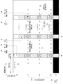
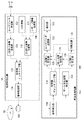
図1は、符号ブロック10におけるエラーの分布状態を示す図である。本図で、縦向きが符号化方向であり、横向きが光ディスクへの記録方向、および光ディスクからの読込方向である。符号ブロック10は、BISコード20、LDC(Long Distance Code)で符号化されたユーザデータ12、LDCパリティ24を含む。BISコード20は、ID情報14、リザーブ情報16、およびBISパリティ18を含む。例えば、ユーザデータ12については、データ216バイトに対して32バイトのパリティが付加され、BISコード20についてはデータ30バイトに対して32バイトのパリティが付加される。本図では、「×」印でエラーの発生箇所を示し、エラーが単発的に生じるランダムエラー30と、連続して生じるバーストエラー36がそれぞれ図示されている。第1バーストエラー36aは、消失訂正により訂正可能な符号列であり、第2バーストエラー36bはバーストエラーとして検出できないため消失訂正により訂正不可能な符号列である。
FIG. 1 is a diagram showing an error distribution state in the
バーストエラーが発生する要因は、ディスクの傷やディスク表面への粉塵の付着である。これらの現象が発生した場合、一般にレーザビームの反射光量に大きな変化が生じる。信号再生回路は通常ヘッドに搭載された光量ディテクタからの出力をヘッドアンプで増幅し、AGCと呼ばれる可変ゲインアンプやイコライザ回路を通してRF波形を整えた後、2値化して復調を行うが、入力信号レベルに大きなトランジェントが生じたり、ヘッドアンプからの出力振幅が極端に低下すると、2値化出力が「ハイ」または「ロー」レベルになり、復調器出力として「0」または「1」が連続して出力されることが多い。 The factors that cause the burst error are scratches on the disk and dust adhering to the disk surface. When these phenomena occur, generally a large change occurs in the amount of reflected laser beam. The signal reproduction circuit usually amplifies the output from the light amount detector mounted on the head with a head amplifier, adjusts the RF waveform through a variable gain amplifier called AGC and an equalizer circuit, and then binarizes and demodulates the input signal. If a large transient occurs in the level or the output amplitude from the head amplifier is extremely reduced, the binarized output becomes “high” or “low” level, and “0” or “1” continues as the demodulator output. Are often output.
ランダムエラー30に対しては、LDCパリティ24を利用して検出訂正が適用される。バーストエラー36に対しては、消失訂正が適用される。消失訂正を行うためには、バーストエラー36の位置を把握する必要がある。このために、BISコード20が利用される。BISコード20は、符号ブロックに対して柵状になるように、予め決められた論理アドレスに配置される。バーストエラー36の位置を推定するために、まずBISパリティ18を利用してBISコード20の誤り訂正が行われ、BISコード20における誤り箇所が特定される。BISコード20は予め決められた論理アドレスに柵状に配置されるので、記録方向で見てBISコード20において誤り訂正が連続した箇所の近傍でバーストエラー36が発生しているとして推定される。そして、その位置を消失位置として消失訂正が行われる。
一般に、リザーブ情報16はビット値として「0」を有しており、バーストエラー36は「1」または「0」の所定のビット値が連続することで出現する。このため、リザーブ情報16をまたいで、ビット値「0」のバーストエラーが生じたとしても、リザーブ情報16のビット値としては誤りでは無いため、BISコード20の訂正を行った場合にも、その位置の訂正は行われない。本図で、「×」印の上に重ねて「○」印を付した第1シンボル32は、BISパリティ18により誤り訂正が行われた位置を示している。 また、「○」印を付した第2シンボル34は、バーストエラーにもかかわらず、誤りとして認識されないことを示す。消失訂正は、BISコード20の誤り訂正位置を手がかりとして、消失訂正位置22を特定して行う。このため、第2シンボル34の様に、BISコード20の誤り訂正が行われない箇所、すなわちユーザデータ12とリザーブ情報16とが一致して見かけ上の誤りが存在しない箇所では、バーストエラー36にも拘わらず誤り位置として検出されない。このため、第2バーストエラー36bの消失位置を推定できず、消失訂正を行うことができない。このように第2バーストエラー36bを検出できないという事態が高い確率で発生する。
Generally, the
本発明はこうした点に鑑みてなされたもので、その目的は、誤り箇所の検出方法、その方法を利用する検出回路、誤り訂正回路、および再生装置を提供することにある。 The present invention has been made in view of these points, and an object thereof is to provide a method for detecting an error location, a detection circuit using the method, an error correction circuit, and a reproducing apparatus.
本発明のある態様は、データ信号に含まれる誤り箇所を検出する方法である。この方法は、データ信号を読み込むステップと、読み込んだデータ信号に含まれる誤り箇所を推定するための検出コード、およびそれに隣接するビット列において所定のビット値が連続しているか否かを判定するステップと、検出コードおよびそれに隣接するビット列において、前記ビット値が連続している場合に、その位置を誤り箇所として推定するステップとを含む。「隣接するビット列」は、時系列的に検出コードの前方または後方に隣接してもよいし、検出コードの前方および後方に隣接してもよい。 One embodiment of the present invention is a method for detecting an error location included in a data signal. The method includes a step of reading a data signal, a step of determining whether or not a predetermined bit value is continuous in a detection code for estimating an error location included in the read data signal and a bit string adjacent thereto. And, when the bit value is continuous in the detection code and the bit string adjacent thereto, estimating the position as an error location. The “adjacent bit string” may be adjacent to the front or rear of the detection code in time series, or may be adjacent to the front and rear of the detection code.
この態様によれば、検出コードとそれに隣接するビット列とに基づいて、データ信号に含まれる誤り箇所を推定するので、検出コードでは検出できない誤り箇所を検出することができる。 According to this aspect, since the error location included in the data signal is estimated based on the detection code and the bit string adjacent thereto, the error location that cannot be detected by the detection code can be detected.
本発明の別の態様は、データ信号に含まれる誤り箇所を検出する回路である。この回路は、データ信号を読み込む読込部と、読み込んだデータ信号に含まれる誤り箇所を推定するための検出コードに基づいて誤り箇所を推定する第1推定部と、読み込んだデータ信号に含まれる検出コードに隣接するビット列の特徴に基づいて、誤り箇所を推定する第2推定部とを備える。「ビット列の特徴」は、例えばビット値に関するものであってよく、「0」または「1」のビット値が連続してどの程度出現しているかなどであってよい。 Another aspect of the present invention is a circuit for detecting an error location included in a data signal. This circuit includes a reading unit that reads a data signal, a first estimation unit that estimates an error location based on a detection code for estimating an error location included in the read data signal, and a detection included in the read data signal A second estimation unit that estimates an error location based on the characteristics of the bit string adjacent to the code. The “characteristic of the bit string” may relate to a bit value, for example, and may indicate how many bit values “0” or “1” appear continuously.
この態様によれば、検出コードに基づいて誤り箇所が推定され、さらに、検出コードに隣接するビット列の特徴に基づいて誤り箇所が推定されるので、検出コードだけでは検出されない誤り箇所も推定される。これにより、誤り箇所の検出能力が向上される。 According to this aspect, the error location is estimated based on the detection code, and further, the error location is estimated based on the characteristics of the bit string adjacent to the detection code. Therefore, the error location that is not detected only by the detection code is also estimated. . Thereby, the detection capability of an error location is improved.
第2推定部は、検出コードとして読み込まれるべきビット値と同一のビット値が連続する場合に、その位置を誤り箇所として推定してもよい。「検出コードとして読み込まれるべきビット値」は、例えばデータ信号に誤りが生じていない場合に、検出コードとして読み込まれるべきビット値であってよい。これにより、見かけ上、検出コードに誤りが生じていない場合にも、第2推定部は誤り箇所を推定できる。 When the same bit value as the bit value to be read as the detection code continues, the second estimation unit may estimate the position as an error location. The “bit value to be read as a detection code” may be a bit value to be read as a detection code when, for example, no error has occurred in the data signal. Thereby, even when an error does not appear in the detection code, the second estimation unit can estimate the error location.
検出コードは、所定の論理アドレスに書き込まれた予め決められたビット値を有してもよい。この場合、第1推定部は検出コードとして読み取られるべきビット値とは異なるビット値の位置を誤り箇所として推定してもよい。 The detection code may have a predetermined bit value written at a predetermined logical address. In this case, the first estimation unit may estimate the position of the bit value different from the bit value to be read as the detection code as the error location.
本発明の更に別の態様は、データ信号に含まれる誤りを訂正する回路である。この回路は、データ信号を読み込む読込部と、読み込んだデータ信号に含まれる誤り箇所を推定するための検出コードに基づいて誤り箇所を推定する第1推定部と、読み込んだデータ信号に含まれる検出コードに隣接するビット列の特徴に基づいて、誤り箇所を推定する第2推定部と、第1推定部および第2推定部により推定された誤り箇所を訂正する訂正部とを備える。これにより、誤り箇所の検出能力が向上され、誤り訂正能力が向上する。 Yet another embodiment of the present invention is a circuit for correcting an error included in a data signal. This circuit includes a reading unit that reads a data signal, a first estimation unit that estimates an error location based on a detection code for estimating an error location included in the read data signal, and a detection included in the read data signal A second estimation unit that estimates an error location based on the characteristics of a bit string adjacent to the code, and a correction unit that corrects the error location estimated by the first estimation unit and the second estimation unit. Thereby, the error location detection capability is improved, and the error correction capability is improved.
本発明の更に別の態様は、記録媒体に記録されたデータ信号を読み込む読込部と、読み込んだデータ信号に含まれる誤り箇所を推定するための検出コードに基づいて誤り箇所を推定する第1推定部と、検出コードに隣接するビット列の特徴に基づいて、誤り箇所を推定する第2推定部と、第1推定部および第2推定部により推定された誤り箇所を訂正する訂正部と、訂正されたデータ信号に基づいて再生を行う再生部とを備える。これにより、誤り箇所の検出能力が向上され、誤り訂正能力が向上されるので、高品質で再生が行われる。 According to still another aspect of the present invention, a reading unit that reads a data signal recorded on a recording medium, and a first estimation that estimates an error location based on a detection code for estimating an error location included in the read data signal A second estimation unit that estimates an error location based on the characteristics of the bit string adjacent to the detection code, a correction unit that corrects the error location estimated by the first estimation unit and the second estimation unit, and A reproducing unit that performs reproduction based on the data signal. As a result, the error location detection capability is improved and the error correction capability is improved, so that reproduction is performed with high quality.
なお、以上の構成要素の任意の組合せ、本発明の表現を方法、装置、システム、記録媒体、コンピュータプログラムなどの間で変換したものもまた、本発明の態様として有効である。 It should be noted that any combination of the above-described constituent elements and a conversion of the expression of the present invention between a method, an apparatus, a system, a recording medium, a computer program, etc. are also effective as an aspect of the present invention.
本発明によれば、検出コードに隣接するデータ列の特徴に基づいて誤り箇所を推定できるので、検出コードに見かけ上、誤りが生じていない場合でも、比較的高い確率で誤り箇所の検出が可能になる。 According to the present invention, the error location can be estimated based on the characteristics of the data string adjacent to the detection code. Therefore, even if no apparent error has occurred in the detection code, the error location can be detected with a relatively high probability. become.
(実施の形態1)
実施の形態1では、データ信号に含まれる誤り箇所の検出方法およびその検出方法を利用する誤り箇所の訂正回路について説明する。
(Embodiment 1)
In the first embodiment, a method for detecting an error location included in a data signal and an error location correction circuit using the detection method will be described.
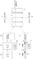
図2は、実施の形態1に係る誤り箇所の検出方法を説明するための図である。本図は、符号ブロック10の一部を示している。符号ブロック10はユーザデータ12およびBISコード20を有する。誤りが生じていない場合、BISコード20のリザーブ情報16は、一般に全てのビット値が「0」を示す。バーストエラーが発生し、第1バーストエラー36aのように、ビット値「1」が連続すると、本来ビット値が「0」となるべきリザーブ情報16が、第1リザーブ情報210のようにビット値「1」となる。第1リザーブ情報210は、BISコード20の訂正処理時に誤り位置として検出される。しかし、第2バーストエラー36bのように、ビット値「0」が連続すると、見かけ上第2リザーブ情報212には誤りが生じていないため、BISコード20の訂正処理時に誤り位置として検出されない。
FIG. 2 is a diagram for explaining the error location detection method according to the first embodiment. This figure shows a part of the
そこで、実施の形態に係る誤り検出方法は、BISコード20に基づいた微視的な検出処理と、BISコード20に隣接するビット列の特徴に基づいた巨視的な検出処理とを組み合わせることにより誤り位置を推定する。すなわち、BISコード20の前方に隣接する第1ビット列214および後方に隣接する第2ビット列216の少なくとも一方が、所定数より多くビット値「0」が連続している場合、その位置が誤り位置として推定される。これにより、リザーブ情報16付近でビット値「0」が連続する第2バーストエラー36bが生じた場合でも、その第2バーストエラー36bを推定することができる。
Therefore, the error detection method according to the embodiment combines the microscopic detection process based on the
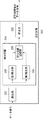
図3は、図2を用いて説明した誤り検出方法を利用して、データ信号に含まれる誤りを訂正する訂正回路220の構成図である。訂正回路220の各構成要素は、種々の電子部品を組み合わせて形成された電子回路であってもよいし、任意のコンピュータのCPU、メモリ、メモリにロードされた本図の構成要素を実現するプログラム、そのプログラムを格納するハードディスクなどの記憶ユニット等によりソフト的に実現されてもよいし、電子回路とソフトウエアとを組み合わせて実現されてもよい。その実現方法、装置にはいろいろな変形例があることは、当業者には理解されるところである。これから説明する各図は、ハードウエア単位の構成ではなく、機能単位のブロックを示している。
FIG. 3 is a configuration diagram of a
読込部222は、データ信号を読み込む。読込部222は、例えば光ディスクなどの記録媒体、放送信号、ネットワークなど任意の提供元からデータ信号を読み込んでよい。検出回路224は、データ信号に含まれる誤り箇所を検出する。訂正部232は、検出回路224に検出された誤り箇所を訂正して、訂正後のデータ信号を出力する。
The
検出回路224は、第1推定部226、第2推定部228、および誤り位置記憶部230を有する。第1推定部226は、図2のBISコード20に訂正処理を施すことにより誤り箇所を推定し、その位置を誤り位置記憶部230に格納する。第2推定部228は、BISコード20に隣接するビット列が所定の特徴の場合、その位置を誤り箇所として推定する。そして、その位置を誤り位置記憶部230に格納する。
The
誤り箇所の位置情報の格納方法は任意でよく、例えば誤りが生じているBISコード20のアドレスを登録してもよいし、符号ブロックごとにマップを用意し、誤り箇所に対応する位置に誤りか否かを示すフラグを登録してもよい。要は、バーストエラーによりデータが消失していると推定される位置が適切に示されるように登録されればよい。以下の説明では、格納方法の種類を問わず、単に「位置を登録する」と表現する。訂正部232は、誤り位置記憶部230に記憶されている誤り位置に基づいて、消失位置を特定して消失訂正を行う。すなわち、訂正部232は、第1推定部226および第2推定部228により推定された誤り箇所の論理和をとり、その位置に対して消失訂正を行う。
The method of storing the location information of the error location may be arbitrary. For example, the address of the
図4は、図3の第2推定部228の内部構成図である。ビット値判定部250は、読込部222から供給されるデータ信号を順次受け付け、各ビットのビット値が所定のビット値であるか否かを判定する。ビット値判定部250が比較対象とするビット値は、誤りが生じていない場合に、リザーブ情報16として読み込まれるべきビット値(以下、単に「理想ビット値」とよぶ)である。すなわち、ビット値判定部250は、データ信号に含まれる各ビットのビット値が理想ビット値であるか否かを判定する。
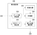
FIG. 4 is an internal block diagram of the
データ信号に含まれるビットのビット値が理想ビット値の場合、ビット値判定部250は計数部254に計数値のインクリメントを指示する。データ信号に含まれるビットのビット値が理想ビット値でない場合、ビット値判定部250は初期化部252に計数部254に計数されている計数値の初期化を指示する。初期化部252は、その指示に基づいて、計数部254における計数値をリセットする。計数部254は、連続する所定のビット値の数を計数し、ビット値判定部250からの指示に基づいてその計数値をインクリメントする。また、計数部254は、初期化部252からの指示に基づいて、計数値をリセット、すなわち「0」に戻す。
When the bit value of the bit included in the data signal is an ideal bit value, the bit
BISコード検出部256は、データ信号に含まれる誤り位置を検出するための検出コード、すなわちBISコード20を検出する。BISコード20は、予め決められた論理アドレスに記録されるため、BISコード検出部256は、予め決められた論理アドレスに位置するビット値をBISコード20として検出する。例えば、BISコード20は、記録方向に対して1バイトの幅を有し、記録方向に対して38バイトの間隔で3つ設けられている。このようにBISコード20が配置されている場合、BISコード検出部256は、38バイト毎に次の1バイトをBISコード20として検出する。
The
BISコード検出部256がBISコード20を検出した場合、誤り位置推定部258は、その時の計数値を計数部254から読み込み、そのBISコード20がバーストエラーの一部か否かを判定する。計数値が所定の範囲に含まれる場合、すなわち最小値Aから最大値Bの間に含まれる場合、誤り位置推定部258はそのBISコード20がバーストエラーの一部であるとして判定する。つまり、誤り位置推定部258は、そのBISコード20の位置を誤り位置として推定する。計数値が所定の範囲に含まれない場合、誤り位置推定部258はそのBISコード20はバーストエラーの一部でないとして判定する。以下、この判定に利用される範囲を、単に「判定基準」とよぶ。一般に、ユーザデータ12には、「1」と「0」とがほぼ同一の割合で出現するようにスクランブルがかけられている。このため、一般的には、「1」や「0」が所定個以上連続して出現することはない。判定基準は、通常のユーザデータ12としては出現し得ない範囲に設定されることが好ましく、例えば変調則から導き出される最大連続長より長い値に設定されてよい。もちろん、実験的に得られた最適値が判定基準として設定されてよい。
When the BIS
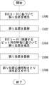
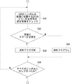
図5は、図3の訂正回路220における訂正処理のフローチャートである。図3の第1推定部226は、データ信号に含まれるBISコード20に基づいて、誤り位置を推定し(S100)、その位置を誤り位置として図3の誤り位置記憶部230に登録する(S102)。図3の第2推定部228は、BISコード20に隣接するビット列の特徴に基づいて、誤り位置を推定し(S104)、その位置を誤り位置として誤り位置記憶部230に登録する(S106)。そして、図3の訂正部232は、誤り位置記憶部230に登録されている誤り位置について論理和をとり、すなわち誤り位置が重複しないようにして、それぞれの誤り位置に基づいて消失訂正を行う(S108)。
FIG. 5 is a flowchart of the correction process in the
(実施の形態2)
実施の形態2では、実施の形態1で説明した誤り箇所の検出方法を利用して、光ディスクから読み込んだデータ信号に対して訂正処理を施す機能を備える装置について説明する。
(Embodiment 2)
In the second embodiment, an apparatus having a function of performing a correction process on a data signal read from an optical disk using the error location detection method described in the first embodiment will be described.
図6は、実施の形態2に係る記録再生装置100の構成図である。記録再生装置100は、記録系処理部136と再生系処理部138とを有する。まず、記録系処理部136について説明する。ユーザデータ受信部102は、例えばホストパソコンあるいはMPEG画像エンコーダ等からのデータを受け取るインタフェースである。LDC訂正符号生成部104は、ユーザデータ受信部102で受信されたデータからパリティを生成してLDCのエラー訂正符号を生成する。ID生成部106は、ユーザデータの光ディスク50における記録位置に対応したアドレス、すなわちID情報を生成する。リザーブ情報生成部108は、BISのエラー訂正符号のデータ部に未使用領域(リザーブ領域)があるとき、リザーブ情報として所定値、例えば16進数で「00」をデータとして生成する。
FIG. 6 is a configuration diagram of the recording / reproducing
BIS訂正符号生成部110は、ID情報およびリザーブ情報に対してパリティを生成してBISのエラー訂正符号を生成する。符号間インタリーブ部112は、LDCのエラー訂正符号とBISのエラー訂正符号に対して、所定のエラー訂正フォーマットに準じてインタリーブ処理を施す。
The BIS correction
図7は、所定のエラー訂正フォーマットを有する符号ブロック10の生成手順を示す図である。図6のユーザデータ受信部102はユーザデータ50を受信する。図6のLDC訂正符号生成部104は、ユーザデータ50に対して、データを記録する方向に直交する符号化方向でエンコードを行い、エンコードされたユーザデータ52とLDCのパリティ56とを生成する。そして、ユーザデータ52とLDCのパリティ56とをあわせてLDCのエラー訂正符号54が生成される。
FIG. 7 is a diagram showing a procedure for generating the
一方、図6のID生成部106は、図6の光ディスク50における記録位置を示すID情報60を生成する。図6のリザーブ情報生成部108は、リザーブ領域が全てビット値「0」になるように、リザーブ情報62を生成する。図6のBIS訂正符号生成部110は、ID情報60およびリザーブ情報62の各データに対して符号化方向でエンコードを行い、エンコードされたID情報64およびリザーブ情報68ならびにBISのパリティ70を生成する。そして、ID情報64、リザーブ情報68、およびBISのパリティ70をあわせてBISのエラー訂正符号72が生成される。LDCのエラー訂正符号54およびBISのエラー訂正符号72は、符号間インタリーブされ、所定のフォーマットに準じて柵状にBISコード20が配置された符号ブロック10となる。光ディスク50へは左側から右側に向かって、上部から順番に記録される。つまり、左上の論理アドレスが一番小さく、右下の論理アドレスが一番大きい。具体的には、まずBISコード20が例えば1バイト光ディスクに記録され、次にLDCのエラー訂正符号すなわちユーザデータ12が例えば38バイト記録され、次にBISコード20が1バイト記録され、ユーザデータ12が38バイト記録されるといった繰り返しになる。
On the other hand, the
図6に戻り、信号記録部114は、符号間インタリーブ部112に生成されたデータを所定の規則にしたがって変調し、変調波形を光ヘッド132に伝達する。光ヘッド132は、光ディスク50に対してレーザビームを照射してデータを記録する。光ヘッド132は、図示しないフォーカストラッキング制御部により制御される。こうして、図7を用いて説明したエラー訂正フォーマットに準じたデータが光ディスク50に記録される。
Returning to FIG. 6, the
次に再生系処理部138について説明する。信号読込部116は、光ディスク50からデータを読み出し、読み出した信号の2値化と復調を行う。符号間デインタリーブ部は、符号間インタリーブ部112と逆の動作、すなわち信号読込部116から得られたデータをLDCのエラー訂正符号とBISのエラー訂正符号に分離してエラー訂正処理を行えるようにする。
Next, the reproduction
BIS誤り訂正部126は、図3の第1推定部226に対応し、BISのエラー訂正符号のエラー訂正を行いID情報を得るとともに、エラー訂正を行った符号ブロック10における位置を誤り位置記憶部124に登録する。ID検出部128は、訂正されたBISのエラー訂正符号からID情報を取り出す。
The BIS
データ消失期間検出部130は、図3の第2推定部228に対応し、データ消失期間検出部130の内部構造は、第2推定部228と同様である。すなわち、データ消失期間検出部130は、BISコード20を検出するBISコード検出部256、連続するビット値「0」の個数を計数する計数部254などを有する。
The data loss
データ消失期間検出部130は、信号読込部116から順次供給されるデインタリーブされる前のデータ信号に基づいて、BISコード20に隣接するビット列のビット値が連続して「0」になる期間を検出する。また、データ消失期間検出部130は、検出した位置に隣接するBISコード20の符号ブロック10における位置を誤り位置記憶部124に登録する。すなわち、データ消失期間検出部130は、BISコード20に隣接するビット列のビット値が「0」で連続する場合、その箇所をバーストエラーの発生箇所として判定する。
The data loss
LDC誤り訂正部120は、詳細は後述するが、ID検出部128から供給されるID情報と誤り位置記憶部124に保持されている誤り位置の情報とに基づいて消失訂正を行うとともに、ランダムエラーに対して検出訂正を行う。ユーザデータ送信部122は、復号されたユーザデータを再生部134に出力する。再生部134は、例えばMPEGデコーダであって、訂正されたユーザデータをデコードして再生を行う。
Although the details will be described later, the LDC
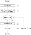
図8は、図6の再生系処理部138における訂正処理のフローチャートである。まず、図6のBIS誤り訂正部126はBISコード20のエラー訂正を行う(S10)。そして、BIS誤り訂正部126は、誤り訂正を行った位置を図6の誤り位置記憶部124に登録する。一方、図6のデータ消失期間検出部130は、図6の信号読込部116から出力されたデインタリーブされる前のデータ信号に含まれる、BISコード20に隣接するビット列の特徴に基づいてバーストエラーの発生箇所を推定する(S14)。そして、データ消失期間検出部130は、推定したバーストエラーの位置を誤り位置として誤り位置記憶部124に登録する。
FIG. 8 is a flowchart of the correction process in the reproduction
図6のLDC誤り訂正部120は、誤り位置記憶部124に保持されている誤り位置の情報を参照して、LDCで消失訂正が可能かどうかの判定を行う(S18)。すなわち、誤り位置記憶部124に保持されている誤り位置の情報を参照して、消失部分があるか否かを判定する。消失訂正が可能な場合(S18のY)、LDC誤り訂正部120は、消失フラグを付加して(S20)、消失訂正を行う(S22)。ステップ18で、消失訂正が不可能な場合(S18のN)、LDC誤り訂正部120は検出訂正を行う(S24)。
The LDC
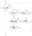
図9は、図8のステップ14における隣接ビット列の特徴に基づいてバーストエラーを推定する処理の詳細なフローチャートである。図6のデータ消失期間検出部130は、読み込んだデータ信号が符号ブロックの終わりを示す最終シンボルであるか否かを判定する(S30)。最終シンボルの場合(S30のY)、図8のステップ18に進む。最終シンボルでない場合(S30のN)、データ消失期間検出部130は読み出したデータのビット値が「0」であるか否かを判定する(S32)。「0」の場合(S32のY)、データ消失期間検出部130は、そのデータがBISコード20であり、かつビット値「0」の計数値が判定基準に含まれるか否かを判定する(S38)。
FIG. 9 is a detailed flowchart of the process of estimating a burst error based on the characteristics of the adjacent bit string in
データがBISコード20であり、かつビット値「0」の計数値が判定基準に含まれる場合(S38のY)、データ消失期間検出部130はそのBISコード20の位置を誤り位置として、図6の誤り位置記憶部124に登録する(S40)。ステップ38で、データがBISコード20であり、かつビット値「0」の計数値が判定基準に含まれるという条件を満たさない場合(S38のN)、データ消失期間検出部130は、「0」の計数値をインクリメントする(S36)。また、ステップ32で、読み出したデータのビット値が「0」でない場合(S32のN)、データ消失期間検出部130は、「0」の計数値を初期化する(S34)。本図は、BISコード20の前方に隣接するビット列を判定対象とするフローチャートであるが、別の例ではBISコード20の後方に隣接するビット列を判定対象としてもよいし、前方および後方に隣接するビット列を判定対象としてもよい。
When the data is the
図10は、図8のステップ20における消失フラグを付加する処理の詳細なフローチャートである。LDCのエラー訂正符号で消失訂正が可能な場合、まず、図6のLDC誤り訂正部120は、符号化方向を見て1バイトづつ、そのバイトからみて前方一番近い位置にあるBISのエラー訂正符号の復号情報、およびそのバイトから見て後方一番近い位置にあるBISのエラー訂正符号の復号情報を、訂正位置記憶用メモリを参照してチェックする(S50)。ここで、「復号情報」は、誤り訂正の有無を示す情報を含む。
FIG. 10 is a detailed flowchart of the process of adding the disappearance flag in
前後両端のBISのエラー訂正符号にエラーがあり訂正されていた場合(S52のY)、LDC誤り訂正部120は、その間のLDCのエラー訂正符号にもバーストエラーが生じているとして推定し、そのバイトに消失フラグを設定する(S54)。ステップ52で、両端のBISのエラー訂正符号でエラーがなく訂正されていない、もしくは片側のみ訂正していた場合(S52のN)、LDC誤り訂正部120は、バーストエラーとはみなさず、消失フラグを付加しない(S56)。そして、これらの処理を全てのシンボルに対して実施した場合(S58のY)、図8のステップ22に進む。また、全てのシンボルに対して実施していない場合(S58のN)、ステップ50に戻る。
If there is an error in the BIS error correction codes at the front and rear ends and the BDC error correction code has been corrected (Y in S52), the LDC
以上、本発明を実施の形態をもとに説明した。この実施の形態は例示であり、それらの各構成要素や各処理プロセスの組合せにいろいろな変形例が可能なこと、またそうした変形例も本発明の範囲にあることは当業者に理解されるところである。こうした変形例として、図6の記録再生装置100は、光ディスク50にデータを記録し、光ディスク50からデータを読み込むこととしたが、記録媒体は光ディスク50に限らない。例えば、光ヘッド132を磁気ヘッドに換えることで、磁気ディスクを記録媒体としてもよい。
The present invention has been described based on the embodiments. This embodiment is an exemplification, and it will be understood by those skilled in the art that various modifications can be made to combinations of the respective constituent elements and processing processes, and such modifications are also within the scope of the present invention. is there. As such a modification, the recording / reproducing
100 記録再生装置、102 ユーザデータ受信部、104 LDC訂正符号生成部、106 ID生成部、108 リザーブ情報生成部、110 BIS訂正符号生成部、112 符号間インタリーブ部、114 信号記録部、116 信号読込部、118 符号間デインタリーブ部、120 LDC誤り訂正部、122 ユーザデータ送信部、124 誤り位置記憶部、126 BIS誤り訂正部、128 ID検出部、130 データ消失期間検出部、132 光ヘッド、134 再生部、136 記録系処理部、138 再生系処理部、220 訂正回路、222 読込部、224 検出回路、226 第1推定部、228 第2推定部、230 誤り位置記憶部、232 訂正部、250 ビット値判定部、252 初期化部、254 計数部、256 BISコード検出部、258 誤り位置推定部。
100 recording / reproducing apparatus, 102 user data receiving unit, 104 LDC correction code generation unit, 106 ID generation unit, 108 reserve information generation unit, 110 BIS correction code generation unit, 112 inter-code interleave unit, 114 signal recording unit, 116 signal reading 118, inter-code deinterleaving section, 120 LDC error correction section, 122 user data transmission section, 124 error position storage section, 126 BIS error correction section, 128 ID detection section, 130 data loss period detection section, 132 optical head, 134
Claims (8)
読み込んだデータ信号に含まれる誤り箇所を推定するための検出コード、およびそれに隣接するビット列において所定のビット値が連続しているか否かを判定するステップと、
前記検出コードおよびそれに隣接するビット列において、前記ビット値が連続している場合に、その位置を誤り箇所として推定するステップと、
を含むことを特徴とする誤り箇所の検出方法。 Reading the data signal;
A step of determining whether a predetermined bit value is continuous in a detection code for estimating an error location included in the read data signal and a bit string adjacent thereto;
In the detection code and a bit string adjacent thereto, when the bit value is continuous, estimating the position as an error location;
A method for detecting an error location, comprising:
読み込んだデータ信号に含まれる誤り箇所を推定するための検出コードに基づいて誤り箇所を推定する第1推定部と、
読み込んだデータ信号に含まれる前記検出コードに隣接するビット列の特徴に基づいて、誤り箇所を推定する第2推定部と、
を備えることを特徴とする誤り検出回路。 A reading section for reading data signals;
A first estimation unit for estimating an error location based on a detection code for estimating an error location included in the read data signal;
A second estimation unit that estimates an error location based on the characteristics of the bit string adjacent to the detection code included in the read data signal;
An error detection circuit comprising:
前記データ信号を順次読み込みながら同一のビット値が連続して現れるビットの数を計数する計数部と、
前記データ信号を順次読み込みながら前記検出コードを検出する検出部と、
検出された検出コードに隣接するビット列において計数されたビット数が所定の個数より多い場合、その位置を誤り箇所として判定する判定部と、
を備えることを特徴とする請求項4に記載の誤り検出回路。 The second estimation unit includes
A counting unit for counting the number of bits in which the same bit value appears successively while sequentially reading the data signal;
A detection unit for detecting the detection code while sequentially reading the data signal;
When the number of bits counted in the bit string adjacent to the detected code is greater than a predetermined number, a determination unit that determines the position as an error location;
The error detection circuit according to claim 4, further comprising:
読み込んだデータ信号に含まれる誤り箇所を推定するための検出コードに基づいて誤り箇所を推定する第1推定部と、
読み込んだデータ信号に含まれる前記検出コードに隣接するビット列の特徴に基づいて、誤り箇所を推定する第2推定部と、
前記第1推定部および前記第2推定部により推定された誤り箇所を訂正する訂正部と、
を備えることを特徴とする誤り訂正回路。 A reading section for reading data signals;
A first estimation unit for estimating an error location based on a detection code for estimating an error location included in the read data signal;
A second estimation unit that estimates an error location based on the characteristics of the bit string adjacent to the detection code included in the read data signal;
A correction unit for correcting the error portion estimated by the first estimation unit and the second estimation unit;
An error correction circuit comprising:
読み込んだデータ信号に含まれる誤り箇所を推定するための検出コードに基づいて誤り箇所を推定する第1推定部と、
前記検出コードに隣接するビット列の特徴に基づいて、誤り箇所を推定する第2推定部と、
前記第1推定部および前記第2推定部により推定された誤り箇所を訂正する訂正部と、
訂正されたデータ信号に基づいて再生を行う再生部と、
を備えることを特徴とする再生装置。 A reading unit for reading a data signal recorded on a recording medium;
A first estimation unit for estimating an error location based on a detection code for estimating an error location included in the read data signal;
A second estimation unit that estimates an error location based on the characteristics of the bit string adjacent to the detection code;
A correction unit for correcting the error portion estimated by the first estimation unit and the second estimation unit;
A playback unit that performs playback based on the corrected data signal;
A playback apparatus comprising:
Priority Applications (4)
| Application Number | Priority Date | Filing Date | Title |
|---|---|---|---|
| JP2004107934A JP2005293724A (en) | 2004-03-31 | 2004-03-31 | Detection method for error point, error detection circuit using its method, error correction circuit, and reproducing device |
| TW094106541A TWI291813B (en) | 2004-03-31 | 2005-03-04 | Method for detecting an error place, error detecting circuit using such method, error correction circuit, and reproduction device |
| US11/092,894 US7478306B2 (en) | 2004-03-31 | 2005-03-30 | Method of detecting error location, and error detection circuit, error correction circuit, and reproducing apparatus using the method |
| CNB2005100629546A CN100559717C (en) | 2004-03-31 | 2005-03-31 | Error detection method, error detection circuit using same, error correction circuit |
Applications Claiming Priority (1)
| Application Number | Priority Date | Filing Date | Title |
|---|---|---|---|
| JP2004107934A JP2005293724A (en) | 2004-03-31 | 2004-03-31 | Detection method for error point, error detection circuit using its method, error correction circuit, and reproducing device |
Publications (1)
| Publication Number | Publication Date |
|---|---|
| JP2005293724A true JP2005293724A (en) | 2005-10-20 |
Family
ID=35050210
Family Applications (1)
| Application Number | Title | Priority Date | Filing Date |
|---|---|---|---|
| JP2004107934A Pending JP2005293724A (en) | 2004-03-31 | 2004-03-31 | Detection method for error point, error detection circuit using its method, error correction circuit, and reproducing device |
Country Status (4)
| Country | Link |
|---|---|
| US (1) | US7478306B2 (en) |
| JP (1) | JP2005293724A (en) |
| CN (1) | CN100559717C (en) |
| TW (1) | TWI291813B (en) |
Families Citing this family (16)
| Publication number | Priority date | Publication date | Assignee | Title |
|---|---|---|---|---|
| WO2006132331A1 (en) * | 2005-06-10 | 2006-12-14 | International Business Machines Corporation | Error correcting device, method, and program |
| US7890847B2 (en) * | 2007-03-09 | 2011-02-15 | Mediatek Inc. | Apparatus and method for calculating error metrics in a digital communication system |
| US7603591B2 (en) * | 2005-07-19 | 2009-10-13 | Mediatek Incorporation | Apparatus selectively adopting different determining criteria in erasure marking procedure when performing decoding process, and method thereof |
| US7673222B2 (en) * | 2005-07-15 | 2010-03-02 | Mediatek Incorporation | Error-correcting apparatus including multiple error-correcting modules functioning in parallel and related method |
| US7865812B2 (en) * | 2007-02-16 | 2011-01-04 | Mediatek Inc. | Apparatus and method for determining a detected punctured position in punctured convolutional codes |
| US8286051B2 (en) * | 2005-07-15 | 2012-10-09 | Mediatek Inc. | Method and apparatus for burst error detection and digital communication device |
| JP2008310896A (en) * | 2007-06-15 | 2008-12-25 | Spansion Llc | Nonvolatile memory device, nonvolatile memory system, and method for controlling nonvolatile memory device |
| US8095856B2 (en) * | 2007-09-14 | 2012-01-10 | Industrial Technology Research Institute | Method and apparatus for mitigating memory requirements of erasure decoding processing |
| US9362953B2 (en) * | 2013-08-02 | 2016-06-07 | Infineon Technologies Ag | Efficient error correction of multi-bit errors |
| US9923664B2 (en) * | 2014-10-01 | 2018-03-20 | Samsung Display Co., Ltd. | Common-mode signaling for transition encoding |
| JP2017055254A (en) * | 2015-09-09 | 2017-03-16 | 株式会社東芝 | Data recovery circuit, semiconductor storage device and data recovery method |
| US10565513B2 (en) | 2016-09-19 | 2020-02-18 | Applied Materials, Inc. | Time-series fault detection, fault classification, and transition analysis using a K-nearest-neighbor and logistic regression approach |
| TWI603190B (en) * | 2016-09-30 | 2017-10-21 | 旺宏電子股份有限公司 | Electronic device and method for finding error locations in a codeword |
| CN107919876B (en) * | 2016-10-09 | 2021-03-12 | 旺宏电子股份有限公司 | Method and electronic device for finding error locations in a codeword |
| JP2019053802A (en) * | 2017-09-14 | 2019-04-04 | 株式会社東芝 | Storage device and control method |
| US11664084B2 (en) | 2021-08-02 | 2023-05-30 | Micron Technology, Inc. | Memory device on-die ECC data |
Family Cites Families (7)
| Publication number | Priority date | Publication date | Assignee | Title |
|---|---|---|---|---|
| US5631909A (en) * | 1995-05-31 | 1997-05-20 | Quantum Corporation | Method and apparatus for determining burst errors in an error pattern |
| US6052815A (en) * | 1997-11-14 | 2000-04-18 | Cirrus Logic, Inc. | ECC system for generating a CRC syndrome over randomized data in a computer storage device |
| US6378100B1 (en) * | 1997-12-29 | 2002-04-23 | U.S. Philips Corporation | Method and apparatus for encoding multiword information with error locative clues directed to low protectivity words |
| CZ301101B6 (en) | 1997-12-29 | 2009-11-04 | Koninklijke Philips Electronics N. V. | Method for encoding and decoding multiword information, device for encoding, decoding, and physical carrier created by encoding method |
| JP2003036608A (en) | 2001-07-19 | 2003-02-07 | Matsushita Electric Ind Co Ltd | Optical disk, optical disk device, error correction format, and data recording / reproducing method |
| JP3993035B2 (en) * | 2001-07-19 | 2007-10-17 | 松下電器産業株式会社 | Data recording method, recording medium, and reproducing apparatus |
| JP4223302B2 (en) * | 2003-03-13 | 2009-02-12 | 富士通株式会社 | Transmission apparatus and burst error monitoring method |
-
2004
- 2004-03-31 JP JP2004107934A patent/JP2005293724A/en active Pending
-
2005
- 2005-03-04 TW TW094106541A patent/TWI291813B/en not_active IP Right Cessation
- 2005-03-30 US US11/092,894 patent/US7478306B2/en not_active Expired - Fee Related
- 2005-03-31 CN CNB2005100629546A patent/CN100559717C/en not_active Expired - Fee Related
Also Published As
| Publication number | Publication date |
|---|---|
| CN100559717C (en) | 2009-11-11 |
| TWI291813B (en) | 2007-12-21 |
| CN1677874A (en) | 2005-10-05 |
| US20050229070A1 (en) | 2005-10-13 |
| US7478306B2 (en) | 2009-01-13 |
| TW200534597A (en) | 2005-10-16 |
Similar Documents
| Publication | Publication Date | Title |
|---|---|---|
| US7137045B2 (en) | Decoding method and apparatus therefor | |
| JP4268619B2 (en) | Recording medium, reproducing apparatus and recording apparatus | |
| JP2005293724A (en) | Detection method for error point, error detection circuit using its method, error correction circuit, and reproducing device | |
| EP1182785B1 (en) | Data processing method and apparatus | |
| KR100265769B1 (en) | Error correction device in an optical disc system and error correction method therefor | |
| US8370703B2 (en) | Information encoding method, information decoding method, recording/reproducing apparatus, and information storage medium | |
| US20090190451A1 (en) | Data storage medium reproducing device and method for reproducing data storage medium | |
| US7430702B2 (en) | Data recording/reproducing apparatus and data recording/reproducing method | |
| JP2004532571A (en) | Method and apparatus for encoding an information word, method and apparatus for decoding an information word, storage medium and signal | |
| JP2003036608A (en) | Optical disk, optical disk device, error correction format, and data recording / reproducing method | |
| US6819642B2 (en) | Data recording device, data reproducing device, and optical disc | |
| US20090195421A1 (en) | Method and apparatus for controlling digital sum value and recording medium for executing the method | |
| JP4079906B2 (en) | Error correction circuit and reproducing apparatus | |
| KR20040017383A (en) | Apparatus and method for modulating address data, apparatus and method demodulating address data therefor, and recording medium for recording modulated address data | |
| JP2005209286A (en) | Data recording method, recording medium, and reproducing device | |
| US7486209B2 (en) | Demodulation table, demodulating device and demodulating method, program, and recording medium | |
| JPWO2004053873A1 (en) | Data recording / playback system | |
| JP4484813B2 (en) | REPRODUCTION DEVICE, RECORDING DEVICE, REPRODUCTION METHOD, AND RECORDING METHOD | |
| JP2005142812A (en) | Error correction method, error correction circuit, and information reproducing apparatus | |
| US20100188272A1 (en) | Method and apparatus for embedding second code into optical disc data by data modulation rule variation | |
| KR20090100611A (en) | Data error correction method and apparatus | |
| JP2007273017A (en) | Information reproducing apparatus, error correction method, and integrated circuit | |
| JP2006172563A (en) | Disc recording / reproducing apparatus, disc recording circuit and reproducing circuit | |
| JP2007035132A (en) | Optical disk processing apparatus and method | |
| JP2006277842A (en) | REPRODUCTION DEVICE, REPRODUCTION METHOD, AND PROGRAM |
Legal Events
| Date | Code | Title | Description |
|---|---|---|---|
| A621 | Written request for application examination |
Free format text: JAPANESE INTERMEDIATE CODE: A621 Effective date: 20060721 |
|
| A977 | Report on retrieval |
Free format text: JAPANESE INTERMEDIATE CODE: A971007 Effective date: 20070910 |
|
| A131 | Notification of reasons for refusal |
Free format text: JAPANESE INTERMEDIATE CODE: A131 Effective date: 20070918 |
|
| A521 | Request for written amendment filed |
Free format text: JAPANESE INTERMEDIATE CODE: A523 Effective date: 20071023 |
|
| A02 | Decision of refusal |
Free format text: JAPANESE INTERMEDIATE CODE: A02 Effective date: 20071113 |