JP2005293667A - Optical pickup device and optical system unit - Google Patents
Optical pickup device and optical system unit Download PDFInfo
- Publication number
- JP2005293667A JP2005293667A JP2004104252A JP2004104252A JP2005293667A JP 2005293667 A JP2005293667 A JP 2005293667A JP 2004104252 A JP2004104252 A JP 2004104252A JP 2004104252 A JP2004104252 A JP 2004104252A JP 2005293667 A JP2005293667 A JP 2005293667A
- Authority
- JP
- Japan
- Prior art keywords
- optical
- pickup device
- optical element
- optical pickup
- information recording
- Prior art date
- Legal status (The legal status is an assumption and is not a legal conclusion. Google has not performed a legal analysis and makes no representation as to the accuracy of the status listed.)
- Pending
Links
- 230000003287 optical effect Effects 0.000 title claims abstract description 162
- 230000004075 alteration Effects 0.000 claims description 25
- 239000011241 protective layer Substances 0.000 claims description 15
- 238000006243 chemical reaction Methods 0.000 claims description 8
- 238000001746 injection moulding Methods 0.000 claims description 8
- 230000008859 change Effects 0.000 claims description 7
- 230000004907 flux Effects 0.000 claims description 3
- 239000008186 active pharmaceutical agent Substances 0.000 description 12
- 239000010410 layer Substances 0.000 description 8
- 239000000919 ceramic Substances 0.000 description 6
- 239000004065 semiconductor Substances 0.000 description 6
- 238000001514 detection method Methods 0.000 description 3
- 230000010287 polarization Effects 0.000 description 3
- 230000015556 catabolic process Effects 0.000 description 2
- 230000008602 contraction Effects 0.000 description 2
- 238000006731 degradation reaction Methods 0.000 description 2
- 230000006866 deterioration Effects 0.000 description 2
- 238000010586 diagram Methods 0.000 description 2
- 230000005484 gravity Effects 0.000 description 2
- 238000004519 manufacturing process Methods 0.000 description 2
- 230000007246 mechanism Effects 0.000 description 2
- 230000004044 response Effects 0.000 description 2
- 206010010071 Coma Diseases 0.000 description 1
- 235000005811 Viola adunca Nutrition 0.000 description 1
- 240000009038 Viola odorata Species 0.000 description 1
- 235000013487 Viola odorata Nutrition 0.000 description 1
- 235000002254 Viola papilionacea Nutrition 0.000 description 1
- 230000008901 benefit Effects 0.000 description 1
- 230000008878 coupling Effects 0.000 description 1
- 238000010168 coupling process Methods 0.000 description 1
- 238000005859 coupling reaction Methods 0.000 description 1
- 239000013078 crystal Substances 0.000 description 1
- NKZSPGSOXYXWQA-UHFFFAOYSA-N dioxido(oxo)titanium;lead(2+) Chemical compound [Pb+2].[O-][Ti]([O-])=O NKZSPGSOXYXWQA-UHFFFAOYSA-N 0.000 description 1
- 238000006073 displacement reaction Methods 0.000 description 1
- 230000006872 improvement Effects 0.000 description 1
- 238000010030 laminating Methods 0.000 description 1
- 238000000034 method Methods 0.000 description 1
- 230000000630 rising effect Effects 0.000 description 1
- 238000007493 shaping process Methods 0.000 description 1
- 238000005549 size reduction Methods 0.000 description 1
- 238000003860 storage Methods 0.000 description 1
- 239000000758 substrate Substances 0.000 description 1
- 230000002195 synergetic effect Effects 0.000 description 1
- 229910052845 zircon Inorganic materials 0.000 description 1
- GFQYVLUOOAAOGM-UHFFFAOYSA-N zirconium(iv) silicate Chemical compound [Zr+4].[O-][Si]([O-])([O-])[O-] GFQYVLUOOAAOGM-UHFFFAOYSA-N 0.000 description 1
Images


Landscapes
- Optical Head (AREA)
- Optical Recording Or Reproduction (AREA)
Abstract
Description
本発明は、光ピックアップ装置及び光学系ユニットに関し、特に光情報記録媒体に対して適切に情報の記録及び/又は再生を行える光ピックアップ装置及び光学系ユニットに関する。 The present invention relates to an optical pickup device and an optical system unit, and more particularly to an optical pickup device and an optical system unit capable of appropriately recording and / or reproducing information with respect to an optical information recording medium.
近年、短波長赤色半導体レーザの実用化に伴い、従来の光ディスク(「光情報記録媒体」ともいう)である、CD(コンパクトディスク)と同程度の大きさで大容量化させた高密度の光ディスクであるDVD(デジタルバーサタイルディスク)が開発・製品化されているが、近い将来には、より高密度な次世代の光ディスクが登場することが予想されている。このような次世代の光ディスクを媒体とした光ピックアップ装置の光学系では、記録信号の高密度化、或いは高密度記録信号の再生のために、光源であるレーザの短波長化とともに対物レンズの高開口数(Nurmerical Aperture:NA)化が図られている。 In recent years, along with the practical use of short-wavelength red semiconductor lasers, high-density optical disks with the same size and large capacity as conventional optical disks (also called “optical information recording media”), CDs (compact disks). The DVD (Digital Versatile Disc) is being developed and commercialized, but it is expected that the next generation optical disc with higher density will appear in the near future. In such an optical system of an optical pickup device using a next-generation optical disk as a medium, in order to increase the recording signal density or to reproduce the high-density recording signal, the wavelength of the laser as a light source is shortened and the objective lens is increased. A numerical aperture (NA) is being achieved.
しかしながら、対物レンズの高NA化が図られてくると、CDやDVDのごとき比較的低密度な光ディスクを記録または再生する場合においてほとんど無視できた問題でもより顕在化されることが予想される。 However, if the NA of the objective lens is increased, it is expected that problems that can be almost ignored when recording or reproducing an optical disk having a relatively low density such as a CD or DVD will become more apparent.
その問題の1つが、光ディスクの保護層(「透明基板」ともいう)の厚み誤差により生じる球面収差である。この球面収差は対物レンズの開口数の4乗に比例して発生する。開口数が比較的小さい従来のCDやDVDの場合には保護層の厚さの誤差による球面収差の発生量は十分小さいので、特別に球面収差を補正する必要はなかった。これに対し、対物レンズの開口数が大きくなった場合、例えば開口数を0.85とした場合には、保護層の厚み誤差の許容値は10μm以下となってしまう。ところが、現状の光ディスクの製造方法では安定して10μm以下の厚み誤差とすることは難しく、量産として成立しない恐れがある。したがって、光学系において光ディスクの保護層の厚み誤差による球面収差を補正する必要がある。しかし、その場合には光ディスクに対する情報の記録または再生を行いながら、リアルタイムで光ディスクの保護層の厚み誤差による球面収差を補正する必要があるので、球面収差を補正する手段には高速な応答が要求される。 One of the problems is spherical aberration caused by the thickness error of the protective layer (also referred to as “transparent substrate”) of the optical disk. This spherical aberration occurs in proportion to the fourth power of the numerical aperture of the objective lens. In the case of a conventional CD or DVD having a relatively small numerical aperture, the amount of spherical aberration generated due to an error in the thickness of the protective layer is sufficiently small, and it is not necessary to specifically correct spherical aberration. On the other hand, when the numerical aperture of the objective lens is increased, for example, when the numerical aperture is 0.85, the tolerance value of the thickness error of the protective layer is 10 μm or less. However, it is difficult to make a thickness error of 10 μm or less stably in the current optical disc manufacturing method, and there is a possibility that it cannot be established as mass production. Therefore, it is necessary to correct the spherical aberration due to the thickness error of the protective layer of the optical disk in the optical system. However, in that case, it is necessary to correct spherical aberration due to the thickness error of the protective layer of the optical disc in real time while recording or reproducing information on the optical disc, and therefore, a high-speed response is required for the means for correcting the spherical aberration. Is done.
また、高密度な次世代の光ディスクの規格の1つとして、0.1mm程度の保護層を用いることが提案されている。これは、対物レンズが高開口数化されることにより光ディスクのそりや傾きによって大きく生じるコマ収差を抑えるためである。ところが、これによりCDやDVDと大きく保護層の厚さが異なってしまうので、少なくとも共通の対物レンズを用いることにより、コストを大幅に増大させることなく、これらの様々な規格の光ディスクの間の互換性をとることが要求される。 In addition, as one of the standards for high-density next-generation optical discs, it has been proposed to use a protective layer of about 0.1 mm. This is to suppress coma aberration, which is largely caused by warping or tilting of the optical disk due to the increase in the numerical aperture of the objective lens. However, since the thickness of the protective layer is greatly different from that of CDs and DVDs, compatibility between optical discs of these various standards can be achieved at least by using a common objective lens without significantly increasing the cost. It is required to take sex.
更に、同一光束入射面側から保護層と情報記録層とを交互に2層積層した構造とすることで、記憶容量を2倍に高めた、いわゆる2層記録DVDが知られているが、次世代の光ディスクシステムでは、DVDよりも高開口数の対物レンズを使用するので、このような2層記録型の光ディスクを記録/再生しようとすると、情報記録層間のフォーカスジャンプの際に光束入射面からそれぞれの情報記録層までの厚さの違いによって球面収差が大きく発生してしまう。従って、次世代の光ディスクシステムでは、情報記録層間のフォーカスジャンプの際は、対物レンズのフォーカシングを行うと同時に球面収差の補正も行わなければならない。 Further, a so-called double-layer recording DVD is known in which the storage capacity is doubled by adopting a structure in which two protective layers and information recording layers are alternately laminated from the same light incident surface side. In the next generation optical disc system, an objective lens having a higher numerical aperture than that of a DVD is used. Therefore, when recording / reproducing such a double-layer recording type optical disc is performed, a focus jump between the information recording layers starts from the light beam incident surface. A large amount of spherical aberration occurs due to the difference in thickness to each information recording layer. Therefore, in the next-generation optical disc system, at the time of a focus jump between information recording layers, the objective lens must be focused and the spherical aberration must be corrected.
加えて、温度により屈折率変化が生じる対物レンズを用いて対物レンズを形成した場合、温度変化に応じて球面収差の劣化が生じるので、その補正を行う必要もある。 In addition, when an objective lens is formed using an objective lens that changes in refractive index with temperature, spherical aberration deteriorates in accordance with the temperature change, and it is necessary to correct it.
これらの問題を解決するために、正レンズと負レンズとからなり、そのうち少なくとも一方を光軸に沿って移動可能としたビームエキスパンダを有する集光光学系が提案されている(特許文献1)。
ここで、上記特許文献1の集光光学系では、温度変化に起因して生じる球面収差の変動や、保護層の厚さの異なる光情報記録媒体の情報記録面に対して情報の記録または再生を行う際に保護層の厚さの違いに起因して発生する球面収差の変動を、第1のアクチュエータにより光学素子を比較的大きな移動量で移動させて補正し、また、記録または再生中に集光光学系で発生する球面収差の変動を第2のアクチュエータにより光学素子を比較的高速にかつ精緻に移動させてリアルタイムに補正している。従って、2つのアクチュエータを搭載しているために、光ピックアップ装置が大型化するという問題がある。 Here, in the condensing optical system of Patent Document 1, information is recorded on or reproduced from information recording surfaces of optical information recording media having different spherical aberration variations caused by temperature changes or different protective layer thicknesses. Of the spherical aberration caused by the difference in the thickness of the protective layer during the recording is corrected by moving the optical element with a relatively large amount of movement by the first actuator, and during recording or reproduction. Variations in spherical aberration occurring in the condensing optical system are corrected in real time by moving the optical element relatively quickly and precisely by the second actuator. Therefore, since the two actuators are mounted, there is a problem that the optical pickup device is enlarged.
一方、複数の光学素子を用いてビームエキスパンダを構成すると、光ピックアップ装置の基準光軸に対して、個々の光学素子の光軸を合わせる必要があり、組付及び調整に手間がかかる。これに対し、アクチュエータとビームエキスパンダを予めユニット化しておけば組付及び調整の手間が軽減されるが、かさばる2つのアクチュエータとビームエキスパンダを組み込んだ上で1つのユニットとすると、かかるユニットをいずれに配置するかなど光ピックアップ装置の設計の自由度が制限されるという問題がある。 On the other hand, when a beam expander is configured by using a plurality of optical elements, it is necessary to align the optical axes of the individual optical elements with respect to the reference optical axis of the optical pickup device, which requires time and effort for assembly and adjustment. On the other hand, if the actuator and beam expander are unitized in advance, the work of assembly and adjustment can be reduced. However, if two actuators and a beam expander are combined into one unit, this unit is There is a problem that the degree of freedom of design of the optical pickup device is limited, such as where it is arranged.
本発明は、かかる従来技術の問題点に鑑みてなされたものであり、組付及び調整の手間を軽減でき、しかも小型化を実現できる光ピックアップ装置及び光学系ユニットを提供することを目的とする。 The present invention has been made in view of the problems of the prior art, and an object of the present invention is to provide an optical pickup device and an optical system unit that can reduce the time and effort of assembly and adjustment and that can be downsized. .
請求項1に記載の光ピックアップ装置は、光源と、前記光源からの光束を光情報記録媒体の情報記録面上に集光させるための対物レンズ、及び前記光源と前記対物レンズとの間の光路中に配置され、収差補正のために光軸方向に移動可能となっている少なくとも一つの光学素子を含む集光光学系と、前記少なくとも一つの光学素子を駆動させる駆動手段と、を有する光ピックアップ装置であって、前記少なくとも一つの光学素子と前記駆動手段とは一体化されており、前記駆動手段は、電気機械変換素子と、前記電気機械変換素子の一端に固定された駆動部材と、前記可動要素に連結され、且つ前記駆動部材上に移動可能に保持された可動部材と、前記電気機械変換素子に電圧を印加する駆動回路とから構成され、前記駆動回路から印加された電圧に応じて前記電気機械変換素子を伸縮させることで、前記駆動部材と前記可動部材を相対移動させるようになっていることを特徴とする。 The optical pickup device according to claim 1, a light source, an objective lens for condensing a light beam from the light source on an information recording surface of an optical information recording medium, and an optical path between the light source and the objective lens An optical pickup having a condensing optical system including at least one optical element disposed therein and movable in the optical axis direction for aberration correction, and drive means for driving the at least one optical element In the apparatus, the at least one optical element and the driving unit are integrated, and the driving unit includes an electromechanical conversion element, a driving member fixed to one end of the electromechanical conversion element, The movable member is connected to the movable element and movably held on the drive member, and a drive circuit that applies a voltage to the electromechanical transducer, and is applied from the drive circuit. By expanding and contracting the electromechanical transducer in accordance with the voltage, characterized in that it is the movable member and the drive member so as to relatively move.
前記駆動手段において、前記駆動回路より前記電気機械変換素子に対して鋸歯状の波形をしたパルスなどの駆動電圧をごく短時間印加することで、前記電気機械変換素子を微少に伸長または収縮するように変形させることができるが、そのパルスの形状により伸長又は収縮の速度を変えることができる。ここで、前記電気機械変換素子を伸長または収縮方向へ速い速度で変形したとき、前記可動部材は、その質量の慣性により、前記駆動部材の動作に追随せず、そのままの位置に留まる。一方、電気機械変換素子がそれよりも遅い速度で反対方向へと変形したとき、前記可動部材は、その間に作用する摩擦力で駆動部材の動作に追随して移動する。したがって、前記電気機械変換素子が伸縮を繰り返すことにより、前記可動部材は一方向へ連続して移動することができる。即ち、本発明の駆動手段を用いることで、前記可動部材に連結した光学素子を大きな移動量で移動させることもでき、或いは小さな移動量で移動させることもできる。従って、特許文献1に開示されているような2つの特性の異なるアクチュエータは不要となり、装置のコンパクト化を図ることができる。尚、「光軸方向に移動可能な少なくとも1つの光学素子」とは、例えばエキスパンダー光学系を構成する光学素子であっても良く、カップリングレンズであっても良い。 In the drive means, the drive circuit applies a drive voltage such as a sawtooth-shaped pulse to the electromechanical conversion element for a very short time so that the electromechanical conversion element is slightly expanded or contracted. The speed of expansion or contraction can be changed depending on the shape of the pulse. Here, when the electromechanical conversion element is deformed at a high speed in the extending or contracting direction, the movable member does not follow the operation of the driving member due to the inertia of the mass and remains in the same position. On the other hand, when the electromechanical conversion element is deformed in the opposite direction at a slower speed, the movable member moves following the operation of the driving member by the friction force acting therebetween. Therefore, when the electromechanical conversion element repeats expansion and contraction, the movable member can continuously move in one direction. That is, by using the driving means of the present invention, the optical element connected to the movable member can be moved with a large amount of movement, or can be moved with a small amount of movement. Therefore, an actuator having two different characteristics as disclosed in Patent Document 1 is not required, and the apparatus can be made compact. The “at least one optical element movable in the optical axis direction” may be, for example, an optical element that constitutes an expander optical system or a coupling lens.
請求項2に記載の光ピックアップ装置は、請求項1に記載の発明において、前記集光光学系は、前記少なくとも1つの光学素子と、それとは異なる光学素子とが射出成形により形成されていることを特徴とする。例えば光学素子がプラスチックを射出成形してなるような場合、かかる光学素子にはゲートの位置に起因して、わずかに回転非対称な光学特性が残存する恐れがある。複数の光学素子に、そのような回転非対称な光学特性が残存した場合、それらの位相を合わせたときに、相乗効果によって狙い通りの光学特性を得られない恐れがある。そこで、光学素子の組付に当たっては、回転非対称な光学特性の位相をずらすことが求められるが、一般的には光学素子を製造するメーカーとは異なるの光ピックアップ装置のメーカーにおいて、組付時に、いちいち光学素子の方向をチェックしながら組み付けるのでは手間がかかる。一方、光学素子を製造するメーカーは、光学素子に対するゲート位置を把握しているという実状がある。そこで、本発明のように、前記駆動手段に一体化してなる前記少なくとも1つの光学素子と、それとは異なる光学素子の位相を予め合わせた状態で、光ピックアップ装置のメーカーに納入するようにすれば、光学素子のゲート位置の位相をずらすことが容易にでき、高い光学特性を確保しながらも組付性の向上に貢献することとなる。 According to a second aspect of the present invention, in the optical pickup device according to the first aspect, the condensing optical system includes the at least one optical element and a different optical element formed by injection molding. It is characterized by. For example, when the optical element is formed by injection molding of plastic, there is a risk that the optical element may have slightly rotationally asymmetric optical characteristics due to the position of the gate. When such rotationally asymmetric optical characteristics remain in a plurality of optical elements, there is a possibility that the target optical characteristics cannot be obtained due to a synergistic effect when their phases are matched. Therefore, when assembling the optical element, it is required to shift the phase of the rotationally asymmetric optical characteristics, but in general, in the manufacturer of the optical pickup device different from the manufacturer that manufactures the optical element, It takes time and effort to assemble while checking the direction of the optical element. On the other hand, there is a fact that a manufacturer that manufactures an optical element knows a gate position with respect to the optical element. Therefore, as in the present invention, if the phase of the at least one optical element integrated with the driving unit and the optical element different from the at least one optical element are matched in advance, it is delivered to the manufacturer of the optical pickup device. The phase of the gate position of the optical element can be easily shifted, which contributes to the improvement of the assembling property while ensuring high optical characteristics.
請求項3に記載の光ピックアップ装置は、請求項1又は2に記載の発明において、前記対物レンズはプラスチックから形成されており、温度変化に起因して発生する球面収差の変動を、前記少なくとも1つの光学素子を光軸方向に移動させることで補正するようになっていることを特徴とする。 According to a third aspect of the present invention, in the optical pickup device according to the first or second aspect, the objective lens is made of plastic, and the variation of the spherical aberration caused by the temperature change is the at least one. The correction is made by moving one optical element in the direction of the optical axis.
請求項4に記載の光ピックアップ装置は、請求項1又は2に記載の発明において、前記光ピックアップ装置は、保護層の厚さの異なる光情報記録媒体の情報記録面に対してそれぞれ情報の記録および/または再生が可能となっており、光情報記録媒体の保護層の厚さの違いに起因して発生する球面収差の変動を、前記少なくとも1つの光学素子を光軸方向に移動させることで補正するようになっていることを特徴とする。 According to a fourth aspect of the present invention, there is provided the optical pickup device according to the first or second aspect, wherein the optical pickup device records information on information recording surfaces of optical information recording media having different protective layer thicknesses. And / or reproduction is possible, and the variation of the spherical aberration caused by the difference in the thickness of the protective layer of the optical information recording medium is moved by moving the at least one optical element in the optical axis direction. It is characterized by correction.
請求項5に記載の光ピックアップ装置は、請求項1〜4のいずれかに記載の発明において、前記光源は、少なくとも380〜450nmの波長の光束を出射することを特徴とする。 According to a fifth aspect of the present invention, in the invention according to any one of the first to fourth aspects, the light source emits a light beam having a wavelength of at least 380 to 450 nm.
請求項6に記載の光学系ユニットは、請求項1〜5のいずれかに記載の光ピックアップ装置に用いられ、前記少なくとも1つの光学素子と前記駆動手段とを一体化してなることを特徴とする。 An optical system unit according to a sixth aspect is used in the optical pickup device according to any one of the first to fifth aspects, wherein the at least one optical element and the driving unit are integrated. .
本発明によれば、組付及び調整の手間を軽減でき、しかも小型化を実現できる光ピックアップ装置及び光学系ユニットを提供することができる。 ADVANTAGE OF THE INVENTION According to this invention, the effort of an assembly | attachment and adjustment can be reduced, and also the optical pick-up apparatus and optical system unit which can implement | achieve size reduction can be provided.
以下、本発明の実施の形態を図面を参照して説明する。図1は、2層構造の光情報記録媒体(光ディスクともいう)ODのいずれの情報記録面に対しても適切に情報の記録/再生を行える光ピックアップ装置の構成を概略的に示す図である。尚、光源波長λは405nmであるが、655nmでもよい。 Hereinafter, embodiments of the present invention will be described with reference to the drawings. FIG. 1 is a diagram schematically showing a configuration of an optical pickup apparatus capable of appropriately recording / reproducing information on any information recording surface of an optical information recording medium (also called an optical disc) OD having a two-layer structure. . The light source wavelength λ is 405 nm, but may be 655 nm.
図1の光ピックアップ装置は、光ディスクODに対して情報の記録/再生を行う場合に発光され、405nmのレーザ光束を射出する光源(半導体レーザ)LDと、光ディスクODの情報記録面からの反射光束を受光する光検出器PDと、コリメートレンズCOL、プリズムペアPP、偏光ビームスプリッタPBS、エキスパンダー光学系EXP、1/4波長板QWP、絞りAP、対物レンズOBJを含む集光光学系とを有している。 The optical pickup device of FIG. 1 emits light when recording / reproducing information with respect to the optical disc OD and emits a laser beam of 405 nm (semiconductor laser) LD, and a reflected light beam from the information recording surface of the optical disc OD. And a condensing optical system including a collimating lens COL, a prism pair PP, a polarizing beam splitter PBS, an expander optical system EXP, a quarter-wave plate QWP, an aperture AP, and an objective lens OBJ. ing.
図1の光ピックアップ装置において、半導体レーザLDから出射された光束は、コリメートレンズCOLで平行光束とされた後、プリズムペアPSを通過する際にビーム整形を施され、更に偏光ビームスプリッタPBSを通過して、エキスパンダー光学系EXPに至る。エキスパンダー光学系EXPは、凹レンズL1と凸レンズL2とを有し、レンズL1、L2の光軸方向の間隔を変更することによって、情報を記録及び/又は再生すべき情報記録面R1,R2の保護層の厚さに起因する収差補正を可能にする。又、同時に温度変化に起因した球面収差劣化の補正を行ってもよい。 In the optical pickup device of FIG. 1, the light beam emitted from the semiconductor laser LD is converted into a parallel light beam by the collimator lens COL, and then subjected to beam shaping when passing through the prism pair PS, and further passes through the polarization beam splitter PBS. Then, the expander optical system EXP is reached. The expander optical system EXP has a concave lens L1 and a convex lens L2, and changes the distance between the lenses L1 and L2 in the optical axis direction to record and / or reproduce information on the information recording surfaces R1 and R2 that are protective layers. Aberration correction due to the thickness of the lens can be corrected. At the same time, spherical aberration deterioration due to temperature change may be corrected.
エキスパンダー光学系EXPを通過した光束は、1/4波長板QWP、絞りAPを通過し、対物レンズOBJに入射して、ここから光ディスクODの情報記録面R1,R2のいずれかに集光される。 The light beam that has passed through the expander optical system EXP passes through the quarter-wave plate QWP and the aperture AP, enters the objective lens OBJ, and is collected from here on one of the information recording surfaces R1 and R2 of the optical disc OD. .
いずれかの情報記録面R1、R2で情報ピットにより変調された反射光束は、再び対物レンズOBJ、絞りAP、1/4波長板QWP、エキスパンダー光学系EXPを通過し、偏光ビームスプリッタPBSで反射されて、シリンドリカルレンズCYを通過し、センサレンズSLにより、光検出器PDの受光面に集光されるようになっている。光検出器PDの出力信号を用いて、光ディスクODに情報記録された情報の読み取り信号が得られる。 The reflected light flux modulated by the information pits on any of the information recording surfaces R1 and R2 passes again through the objective lens OBJ, the aperture AP, the quarter wavelength plate QWP, and the expander optical system EXP, and is reflected by the polarization beam splitter PBS. Thus, the light passes through the cylindrical lens CY and is condensed on the light receiving surface of the photodetector PD by the sensor lens SL. A read signal of information recorded on the optical disk OD is obtained using the output signal of the photodetector PD.
また、光検出器PD上でのスポットの形状変化、位置変化による光量変化を検出して、合焦検出やトラック検出を行う。この検出に基づいて対物レンズアクチュエータ機構ACTのフォーカシングアクチュエータ及びトラッキングアクチュエータが、半導体レーザLDからの光束を光ディスクODの情報記録面上に適切に結像するように、対物レンズOBJを一体で移動させるようになっている。 In addition, focus detection and track detection are performed by detecting a change in the amount of light due to a change in the shape and position of the spot on the photodetector PD. Based on this detection, the objective lens OBJ is moved integrally so that the focusing actuator and tracking actuator of the objective lens actuator mechanism ACT appropriately image the light flux from the semiconductor laser LD on the information recording surface of the optical disc OD. It has become.
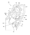
図2は、エキスパンダー光学系EXPと、その駆動手段とを一体的に収納した光学系ユニットXUの斜視図である。図2において、ベースBの両端から上方に壁W1,W2が延在している。壁W1,W2(切り欠いて図示)の上端近傍を連結するようにしてガイド軸GSが延在している。壁W1,W2にはそれぞれ光束が通過する開孔HLが形成されている。 FIG. 2 is a perspective view of an optical system unit XU that integrally accommodates the expander optical system EXP and its driving means. In FIG. 2, walls W <b> 1 and W <b> 2 extend upward from both ends of the base B. A guide shaft GS extends so as to connect the vicinity of the upper ends of the walls W1 and W2 (notched). Openings HL through which light beams pass are formed in the walls W1 and W2.
プラスチックから射出成形により形成されたレンズL1は、レンズホルダHD1により外周を保持され、壁W1の開孔HLを覆うようにしてビス止めされる。このとき、レンズL1の射出成形時のゲート位置は、例えば光軸から垂直上方の位置にあるようにセットされる(黒三角図示)。尚、レンズL1の組み付けに当たっては、オートコリメータなどを用いて、基準軸に対しシフトやチルトを極力抑えることが望ましい。 The lens L1 formed from plastic by injection molding is held at the outer periphery by the lens holder HD1, and is screwed so as to cover the opening HL of the wall W1. At this time, the gate position at the time of injection molding of the lens L1 is set to be, for example, a position vertically above the optical axis (shown by a black triangle). When assembling the lens L1, it is desirable to suppress shift and tilt with respect to the reference axis as much as possible using an autocollimator or the like.
一方、プラスチックから射出成形により形成されたレンズL2は、レンズホルダHD2により外周を保持されている。可動部材となるレンズホルダHD2は、ガイド軸GSに係合する係合部HDaと、駆動力を受ける駆動部HDbとを有している。かかる状態で、レンズL2の射出成形時のゲート位置は、例えば光軸から垂直下方の位置にあるようにセットされる(黒三角図示)。尚、ガイド軸GSは、必ずしも設ける必要はない。 On the other hand, the outer periphery of the lens L2 formed from plastic by injection molding is held by the lens holder HD2. The lens holder HD2 as a movable member has an engaging portion HDa that engages with the guide shaft GS and a driving portion HDb that receives a driving force. In this state, the gate position at the time of injection molding of the lens L2 is set so as to be at a position vertically below the optical axis, for example (black triangle shown). Note that the guide shaft GS is not necessarily provided.
駆動部HDbは板状であって、上面に板ばねSGを取り付けている。駆動部HDbと板ばねSGとの間には、駆動部材である駆動軸DSが配置され、板ばねSGの付勢力で適度に押圧されている。駆動軸DSの壁W1側は自由端となっており、壁W2側の端部は、圧電アクチュエータPZに連結されている。ベースB上には、駆動部HDbの移動量を検出する不図示のエンコーダから信号を受けて、圧電アクチュエータPZを駆動制御するために電圧を印加する駆動回路DCが配置されている。圧電アクチュエータPZと、駆動軸DSと、駆動部HDbと、板ばねSGと、駆動回路DCとで駆動手段を構成する。尚、駆動回路DCは、ベースBとは別に配置して、配線により連結しても良い。 The drive part HDb is plate-shaped, and a leaf spring SG is attached to the upper surface. A drive shaft DS, which is a drive member, is disposed between the drive portion HDb and the leaf spring SG, and is appropriately pressed by the urging force of the leaf spring SG. The wall W1 side of the drive shaft DS is a free end, and the end portion on the wall W2 side is connected to the piezoelectric actuator PZ. On the base B, a drive circuit DC that receives a signal from an encoder (not shown) that detects the amount of movement of the drive unit HDb and applies a voltage to drive and control the piezoelectric actuator PZ is disposed. The piezoelectric actuator PZ, the drive shaft DS, the drive unit HDb, the leaf spring SG, and the drive circuit DC constitute drive means. The drive circuit DC may be arranged separately from the base B and connected by wiring.
電気機械変換素子である圧電アクチュエータPZは、PZT(ジルコン・チタン酸鉛)などで形成された圧電セラミックスを積層してなる。圧電セラミックスは、その結晶格子内の正電荷の重心と負電荷の重心とが一致しておらず、それ自体分極していて、その分極方向に電圧を印加すると伸びる性質を有している。しかし、圧電セラミックスのこの方向への歪みは微小であり、この歪み量により駆動部材を駆動することは困難であるため、図3に示すように、複数の圧電セラミックスPEを積み重ねてその間に電極Cを並列接続した構造の積層型圧電アクチュエータPZが実用可能なものとして提供されている。本実施の形態では、この積層型圧電アクチュエータPZを駆動源として用いている。 The piezoelectric actuator PZ which is an electromechanical transducer is formed by laminating piezoelectric ceramics formed of PZT (zircon / lead titanate) or the like. Piezoelectric ceramics have a property in which the center of gravity of the positive charge and the center of gravity of the negative charge in the crystal lattice do not coincide with each other, are themselves polarized, and extend when a voltage is applied in the polarization direction. However, since the distortion of the piezoelectric ceramic in this direction is very small and it is difficult to drive the driving member by the amount of the distortion, a plurality of piezoelectric ceramics PE are stacked between the electrodes C as shown in FIG. A multilayer piezoelectric actuator PZ having a structure in which the two are connected in parallel is provided as a practical one. In the present embodiment, this stacked piezoelectric actuator PZ is used as a drive source.
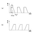
次に、この光学系ユニットXUによるレンズL2の駆動方法について説明する。一般に、積層型圧電アクチュエータPZは、電圧印加時の変位量は小さいが、発生力は大でその応答性も鋭い。したがって、図4(a)に示すように立ち上がりが鋭く立ち下がりがゆっくりとした略鋸歯状波形のパルス電圧を印加すると、圧電アクチュエータPZは、パルスの立ち上がり時に急激に伸び、立ち下がり時にそれよりもゆっくりと縮む。したがって、圧電アクチュエータPZの伸長時には、その衝撃力で駆動軸DSが図2の奥側(壁W1側)へ押し出されるが、レンズL2を保持したレンズホルダHD2の駆動部HDbと板ばねSGは、その慣性により、駆動軸DSと一緒には移動せず、駆動軸DSとの間で滑りを生じてその位置に留まる(わずかに移動する場合もある)。一方、パルスの立ち下がり時には立ち上がり時に比較して駆動軸DSがゆっくりと戻るので、駆動部HDbと板ばねSGが駆動軸DSに対して滑らずに、駆動軸DSと一体的に図2の手前側(壁W2側)へ移動する。即ち、周波数が数百から数万ヘルツに設定されたパルスを印加することにより、レンズホルダHD2を所望の速度で連続的に移動させることができる。尚、以上より明らかであるが、図4(b)に示すように電圧の立ち上がりがゆっくりで、立ち下がりが鋭いパルスを印加すれば、レンズホルダHD2を逆の方向へ移動させることができる。特に、ガイド軸GSがまっすぐであれば、レンズホルダHD2は光軸方向に精度良く移動することとなり、駆動により光軸ずれが生じる場合に比べ、収差劣化を効果的に抑制できる。 Next, a driving method of the lens L2 by the optical system unit XU will be described. In general, the multilayer piezoelectric actuator PZ has a small amount of displacement when a voltage is applied, but has a large generated force and sharp response. Therefore, as shown in FIG. 4 (a), when a pulse voltage having a substantially sawtooth waveform with a sharp rise and a slow fall is applied, the piezoelectric actuator PZ extends rapidly at the rise of the pulse and more than that at the fall. Shrink slowly. Therefore, when the piezoelectric actuator PZ is extended, the driving shaft DS is pushed out to the back side (wall W1 side) in FIG. 2 by the impact force, but the driving portion HDb of the lens holder HD2 holding the lens L2 and the leaf spring SG are Due to its inertia, it does not move together with the drive shaft DS, but slips between the drive shaft DS and stays in that position (may move slightly). On the other hand, when the pulse falls, the drive shaft DS returns more slowly than when the pulse rises. Therefore, the drive portion HDb and the leaf spring SG do not slide with respect to the drive shaft DS, and the drive shaft DS is integrated with the drive shaft DS. Move to the side (wall W2 side). That is, the lens holder HD2 can be continuously moved at a desired speed by applying a pulse whose frequency is set to several hundred to several tens of thousands of hertz. As is clear from the above, the lens holder HD2 can be moved in the opposite direction by applying a pulse in which the voltage rises slowly and sharply falls as shown in FIG. 4B. In particular, if the guide shaft GS is straight, the lens holder HD2 moves with high accuracy in the optical axis direction, and aberration deterioration can be effectively suppressed as compared with the case where the optical axis shift occurs due to driving.
このように鋸歯状の波形をしたパルスの生成は、駆動回路DCのマイクロコンピュータから出力する信号をD/Aコンバータでアナログ信号に変換し、これをアンプで増幅することによって実現できる。波形形状を表す信号は、光検出器PDからの信号に応じて、不図示のメモリに予め記憶されていると好ましいが、例えば駆動軸DSを駆動しながら最適な集光スポットを得るというようなフィードバック制御も可能である。記憶されるデータとしては、例えば図4に示す最大電圧Vmax、電圧のホールド時間t1,t2、立ち上がりと立ち下がりの段数、そのときの1ステップのホールド時間Δtなどがある。なお、図4では、電圧が比較的ゆっくりと変化する部分を直線で示しているが、厳密には、マイクロコンピュータから階段状の信号を出力することで、この波形のパルスを得ている。 The generation of a pulse having a sawtooth waveform can be realized by converting a signal output from the microcomputer of the drive circuit DC into an analog signal by a D / A converter and amplifying it by an amplifier. The signal representing the waveform shape is preferably stored in advance in a memory (not shown) in accordance with the signal from the photodetector PD. For example, an optimum focused spot is obtained while driving the drive axis DS. Feedback control is also possible. The stored data includes, for example, the maximum voltage Vmax shown in FIG. 4, voltage hold times t1 and t2, the number of rising and falling stages, and the hold time Δt for one step at that time. In FIG. 4, the portion where the voltage changes relatively slowly is shown by a straight line. Strictly speaking, a pulse having this waveform is obtained by outputting a stepped signal from a microcomputer.
本実施の形態によれば、単一の圧電アクチュエータPZを用いることで、レンズホルダHD2に保持したレンズL2を大きな移動量で移動させることもでき、或いは小さな移動量で移動させることもできる。従って、保護層の厚さに起因して生じる球面収差の劣化や、温度変化に起因して生じる球面収差の劣化を補正するために、従来技術に開示されているような2つの特性の異なるアクチュエータは不要となり、装置のコンパクト化を図ることができる。 According to the present embodiment, by using a single piezoelectric actuator PZ, the lens L2 held by the lens holder HD2 can be moved with a large movement amount, or can be moved with a small movement amount. Therefore, in order to correct the spherical aberration degradation caused by the thickness of the protective layer and the spherical aberration degradation caused by the temperature change, the actuator having two different characteristics as disclosed in the prior art Is unnecessary, and the apparatus can be made compact.
更に、本実施の形態によれば、レンズL1,L2がプラスチックを射出成形してなるため、ゲートの位置に起因して、わずかに回転非対称な光学特性が残存する恐れがある。そこで、レンズL1,L2の組付に当たっては、回転非対称な光学特性の位相を180度ずらせており、その状態で光学ユニットとして組み付けを行っているので、かかるユニットの状態で、光ピックアップ装置のメーカーに納入でき、高い光学特性を確保しながらも組付性の向上に貢献することとなる。 Furthermore, according to the present embodiment, since the lenses L1 and L2 are formed by injection molding plastic, there is a risk that slightly rotationally asymmetric optical characteristics may remain due to the position of the gate. Therefore, when assembling the lenses L1 and L2, the phase of the rotationally asymmetric optical characteristics is shifted by 180 degrees and the optical unit is assembled in this state. This contributes to improved assembly while ensuring high optical properties.
以上、本発明を実施の形態を参照して説明してきたが、本発明は上記実施の形態に限定して解釈されるべきではなく、適宜変更・改良が可能であることはもちろんである。本発明の光学ユニットは、光源波長が405nm程度の青紫色半導体レーザを備えた光ピックアップ装置や、異なる種類(BD、HD DVD、DVD、CD等)の光ディスクに対して情報の記録及び/又は再生を行える光ピックアップ装置に用いると特に効果がある。 The present invention has been described above with reference to the embodiments. However, the present invention should not be construed as being limited to the above-described embodiments, and can be modified or improved as appropriate. The optical unit according to the present invention records and / or reproduces information with respect to an optical pickup device including a blue-violet semiconductor laser having a light source wavelength of about 405 nm or an optical disc of a different type (BD, HD DVD, DVD, CD, etc.). This is particularly effective when used in an optical pickup device capable of performing the above.
ACT 対物レンズアクチュエータ機構
AP 絞り
B ベース
C 電極
COL コリメートレンズ
CY シリンドリカルレンズ
DS 駆動軸
EXP エキスパンダー光学系
GS ガイド軸
HD1 レンズホルダ
HD2 レンズホルダ
L1 凹レンズ
L2 凸レンズ
LD 半導体レーザ
OBJ 対物レンズ
OD 光ディスク
PBS 偏光ビームスプリッタ
PD 光検出器
PE 圧電セラミックス
PP プリズムペア
PS プリズムペア
PZ 圧電アクチュエータ
PZ 積層型圧電アクチュエータ
QWP 波長板
R1 情報記録面
R1,R2 情報記録面
SL センサレンズ
W1,W2 壁
XU 光学系ユニット
ACT Objective lens actuator mechanism AP Aperture B Base C Electrode COL Collimate lens CY Cylindrical lens DS Drive axis EXP Expander optical system GS Guide axis HD1 Lens holder HD2 Lens holder L1 Concave lens L2 Convex lens LD Semiconductor laser OBJ Objective lens OD Optical disk PBS Polarizing beam splitter PD Photodetector PE Piezoelectric ceramics PP Prism pair PS Prism pair PZ Piezoelectric actuator PZ Laminated piezoelectric actuator QWP Wave plate R1 Information recording surface R1, R2 Information recording surface SL Sensor lens W1, W2 Wall XU Optical system unit
Claims (6)
前記少なくとも一つの光学素子と前記駆動手段とは一体化されており、
前記駆動手段は、
電気機械変換素子と、
前記電気機械変換素子の一端に固定された駆動部材と、
前記可動要素に連結され、且つ前記駆動部材上に移動可能に保持された可動部材と、
前記電気機械変換素子に電圧を印加する駆動回路とから構成され、
前記駆動回路から印加された電圧に応じて前記電気機械変換素子を伸縮させることで、前記駆動部材と前記可動部材を相対移動させるようになっていることを特徴とする光ピックアップ装置。 A light source, an objective lens for condensing the light flux from the light source on the information recording surface of the optical information recording medium, and an optical path between the light source and the objective lens, and light for aberration correction An optical pickup device comprising: a condensing optical system including at least one optical element that is movable in an axial direction; and a driving unit that drives the at least one optical element,
The at least one optical element and the driving means are integrated;
The driving means includes
An electromechanical transducer,
A drive member fixed to one end of the electromechanical transducer;
A movable member coupled to the movable element and held movably on the drive member;
A drive circuit for applying a voltage to the electromechanical transducer,
An optical pickup device, wherein the drive member and the movable member are moved relative to each other by expanding and contracting the electromechanical conversion element in accordance with a voltage applied from the drive circuit.
6. An optical system unit used in the optical pickup device according to claim 1, wherein the at least one optical element and the driving means are integrated.
Priority Applications (1)
| Application Number | Priority Date | Filing Date | Title |
|---|---|---|---|
| JP2004104252A JP2005293667A (en) | 2004-03-31 | 2004-03-31 | Optical pickup device and optical system unit |
Applications Claiming Priority (1)
| Application Number | Priority Date | Filing Date | Title |
|---|---|---|---|
| JP2004104252A JP2005293667A (en) | 2004-03-31 | 2004-03-31 | Optical pickup device and optical system unit |
Publications (1)
| Publication Number | Publication Date |
|---|---|
| JP2005293667A true JP2005293667A (en) | 2005-10-20 |
Family
ID=35326445
Family Applications (1)
| Application Number | Title | Priority Date | Filing Date |
|---|---|---|---|
| JP2004104252A Pending JP2005293667A (en) | 2004-03-31 | 2004-03-31 | Optical pickup device and optical system unit |
Country Status (1)
| Country | Link |
|---|---|
| JP (1) | JP2005293667A (en) |
Cited By (3)
| Publication number | Priority date | Publication date | Assignee | Title |
|---|---|---|---|---|
| JP2007213696A (en) * | 2006-02-09 | 2007-08-23 | Citizen Holdings Co Ltd | Aberration correcting device and optical pickup device using the same |
| JP2009004014A (en) * | 2007-06-20 | 2009-01-08 | Hitachi Media Electoronics Co Ltd | Optical element feeding device, optical pickup device, and optical disk device including the same |
| JP2009004013A (en) * | 2007-06-20 | 2009-01-08 | Hitachi Media Electoronics Co Ltd | Optical element feeding device, optical pickup device, and optical disk device including the same |
-
2004
- 2004-03-31 JP JP2004104252A patent/JP2005293667A/en active Pending
Cited By (3)
| Publication number | Priority date | Publication date | Assignee | Title |
|---|---|---|---|---|
| JP2007213696A (en) * | 2006-02-09 | 2007-08-23 | Citizen Holdings Co Ltd | Aberration correcting device and optical pickup device using the same |
| JP2009004014A (en) * | 2007-06-20 | 2009-01-08 | Hitachi Media Electoronics Co Ltd | Optical element feeding device, optical pickup device, and optical disk device including the same |
| JP2009004013A (en) * | 2007-06-20 | 2009-01-08 | Hitachi Media Electoronics Co Ltd | Optical element feeding device, optical pickup device, and optical disk device including the same |
Similar Documents
| Publication | Publication Date | Title |
|---|---|---|
| JP3992072B2 (en) | Optical pickup device | |
| JP2006202416A (en) | Optical pickup device | |
| CN101165788B (en) | Optical pickup and optical disk drive | |
| JPWO2009047907A1 (en) | Optical pickup device | |
| JPWO2008149522A1 (en) | Optical head device and recording and / or reproducing device | |
| JP2005293667A (en) | Optical pickup device and optical system unit | |
| US7668066B2 (en) | Optical pickup apparatus | |
| JP2005302118A (en) | Optical pickup device | |
| JP2010238277A (en) | Optical pickup device and objective lens unit | |
| JP4285588B2 (en) | Optical pickup device manufacturing method and optical pickup device | |
| JPWO2007010770A1 (en) | Optical pickup device and optical information recording medium recording / reproducing device | |
| JP2009170091A (en) | Optical pickup device and light source unit | |
| JPWO2011033786A1 (en) | Optical pickup optical system | |
| JPWO2007037479A1 (en) | Optical head device | |
| JP2005302243A (en) | Optical pickup device and light source unit | |
| US7706218B2 (en) | Optical pickup apparatus and controlling method thereof | |
| JP2011113581A (en) | Optical pickup device | |
| JP4609332B2 (en) | Optical pickup device | |
| JP4801609B2 (en) | Optical head and optical disk drive | |
| US20060280059A1 (en) | Optical pickup device | |
| JP2006318553A (en) | Optical pickup device | |
| JP2006127705A (en) | Optical pickup device | |
| JP2005293770A (en) | Optical pickup device | |
| JP2010097664A (en) | Objective lens | |
| JP2006155717A (en) | Optical pickup device |
Legal Events
| Date | Code | Title | Description |
|---|---|---|---|
| A621 | Written request for application examination |
Free format text: JAPANESE INTERMEDIATE CODE: A621 Effective date: 20070130 |
|
| A977 | Report on retrieval |
Free format text: JAPANESE INTERMEDIATE CODE: A971007 Effective date: 20090226 |
|
| A131 | Notification of reasons for refusal |
Free format text: JAPANESE INTERMEDIATE CODE: A131 Effective date: 20090304 |
|
| A02 | Decision of refusal |
Free format text: JAPANESE INTERMEDIATE CODE: A02 Effective date: 20090625 |