JP2005293349A - Circuit design support system, design method and program - Google Patents
Circuit design support system, design method and program Download PDFInfo
- Publication number
- JP2005293349A JP2005293349A JP2004108988A JP2004108988A JP2005293349A JP 2005293349 A JP2005293349 A JP 2005293349A JP 2004108988 A JP2004108988 A JP 2004108988A JP 2004108988 A JP2004108988 A JP 2004108988A JP 2005293349 A JP2005293349 A JP 2005293349A
- Authority
- JP
- Japan
- Prior art keywords
- path
- active condition
- data
- transfer
- false
- Prior art date
- Legal status (The legal status is an assumption and is not a legal conclusion. Google has not performed a legal analysis and makes no representation as to the accuracy of the status listed.)
- Withdrawn
Links
Images


Classifications
-
- G—PHYSICS
- G06—COMPUTING OR CALCULATING; COUNTING
- G06F—ELECTRIC DIGITAL DATA PROCESSING
- G06F30/00—Computer-aided design [CAD]
- G06F30/30—Circuit design
Landscapes
- Engineering & Computer Science (AREA)
- Computer Hardware Design (AREA)
- Physics & Mathematics (AREA)
- Theoretical Computer Science (AREA)
- Evolutionary Computation (AREA)
- Geometry (AREA)
- General Engineering & Computer Science (AREA)
- General Physics & Mathematics (AREA)
- Design And Manufacture Of Integrated Circuits (AREA)
Abstract
Description
本発明は、回路設計支援システム、設計方法及びプログラムに関し、特に、動作合成を用いて回路設計を行う回路設計支援システム、設計方法及びプログラムに関する。 The present invention relates to a circuit design support system, a design method, and a program, and more particularly to a circuit design support system, a design method, and a program for performing circuit design using behavioral synthesis.
LSI等の半導体回路は、システム設計、機能設計、論理設計、レイアウト設計等の一連の設計工程を経た後、製造工程により製造される。このような一連の設計工程では、大規模集積回路の設計に対応するため、各種の設計支援システムやプログラムが用いられている。 A semiconductor circuit such as an LSI is manufactured through a manufacturing process after a series of design processes such as system design, functional design, logic design, and layout design. In such a series of design processes, various design support systems and programs are used to cope with the design of a large-scale integrated circuit.
各設計工程の設計レベルでは、その構成内容を明確化するために最適な記述方法を用いて設計が行われている。例えば、機能設計においては、ハードウェアの構造を含まない動作のみを記述した動作記述や、組合せ回路やレジスタ等からなるデータパスや制御回路を記述したRTL(Register Transfer Level)回路等が用いられ、論理設計においては、ゲートの接続関係を記述したネットリスト等が用いられる。 At the design level of each design process, the design is performed using an optimal description method in order to clarify the configuration content. For example, in functional design, an operation description that describes only an operation that does not include a hardware structure, an RTL (Register Transfer Level) circuit that describes a data path or control circuit including a combinational circuit or a register, and the like are used. In the logical design, a net list or the like describing the connection relation of gates is used.
従来、設計者が「Verilog−HDL(Verilog Hardware Description Language)」や「VHDL(VHSIC Hardware Description Language)」等でRTL回路を記述し、これを論理合成によりネットリストに変換する手法が用いられている。近年、さらなる設計効率向上を図るため、設計者がC言語やSystemC等で動作記述を記述し、これを動作合成(高位合成ともいう)によりRTL回路に変換する手法が注目されている。 Conventionally, a method in which an RTL circuit is described by a designer in “Verilog-HDL (Verilog Hardware Description Language)”, “VHDL (VHSIC Hardware Description Language)”, etc., and converted into a netlist by logic synthesis is used. . In recent years, in order to further improve design efficiency, a method in which a designer describes a behavioral description in C language, SystemC, or the like and converts this into an RTL circuit by behavioral synthesis (also referred to as high-level synthesis) has attracted attention.
論理合成では、ネットリスト生成ツールやSTA(静的タイミング解析:Static Timing Analysis)ツール等により、回路がクロックに同期して正常に動作するか否かタイミング検証が行われる。このタイミング検証は、データパスに基づいて行われる。ここで、データパスは、演算器やレジスタ、マルチプレクサ等のインスタンスと、インスタンス間を接続するネットから構成されている。タイミング検証は、複数のネット(転送路ともいう)からなるパス(信号経路)毎に行われ、クロック周期を超えて動作するパスを遅延違反として検出する。このような遅延違反となるパスをクリティカルパスという。 In logic synthesis, timing verification is performed to determine whether a circuit operates normally in synchronization with a clock by a netlist generation tool, a STA (Static Timing Analysis) tool, or the like. This timing verification is performed based on the data path. Here, the data path is composed of instances such as arithmetic units, registers, and multiplexers, and a net connecting the instances. Timing verification is performed for each path (signal path) composed of a plurality of nets (also referred to as transfer paths), and a path that operates beyond the clock cycle is detected as a delay violation. A path that causes such a delay violation is called a critical path.
この時、状態遷移のある回路等において、全ての状態に渡って同時にはアクティブにならないネットを含むパスが存在することがある。このようなパスをフォールスパスといい、いずれかの状態で同時にアクティブになりうるネットを含むパスをトゥルーパスという。尚、アクティブにならないネットとは、活性化しない、つまり、データが転送されないネットをいう。 At this time, in a circuit or the like having a state transition, there may be a path including a net that does not become active simultaneously in all states. Such a path is called a false path, and a path including a net that can be active simultaneously in any state is called a true path. The net that is not active means a net that is not activated, that is, data is not transferred.
論理合成された回路では、トゥルーパスの遅延制約さえ満足していれば、フォールスパスの遅延がいくら大きくなっても回路は正常に動作する。しかし、ネットリスト生成ツールやSTAツール、配置配線ツール等は、どのパスがトゥルーパスであり、どのパスがフォールスパスであるかを判断することができないため、フォールスパスについてもタイミング検証、最適化等を行ってしまう。その結果、論理合成処理時間や回路面積の増大、不要なクリティカルパスを含む遅延レポートの生成等が生じてしまう。 In a logic-synthesized circuit, as long as the true-path delay constraint is satisfied, the circuit operates normally no matter how much the false-path delay increases. However, the netlist generation tool, STA tool, placement and routing tool, etc. cannot determine which path is a true path and which path is a false path. Will go. As a result, an increase in logic synthesis processing time and circuit area, generation of a delay report including unnecessary critical paths, and the like occur.
このため、ネットリスト生成ツール等にどのパスがフォールスパスであるか設定し、フォールスパスについては、論理合成やタイミング検証を行わないのが一般的である。ネットリスト生成ツール等にフォールスパスを設定するために、動作合成後の回路情報からフォールスパスを抽出する方法が知られている(例えば、特許文献1、2参照)。
For this reason, it is common to set which path is a false path in a netlist generation tool or the like, and for the false path, logic synthesis and timing verification are not performed. In order to set a false path in a netlist generation tool or the like, a method for extracting a false path from circuit information after behavioral synthesis is known (for example, see
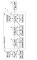
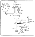
図16に、従来のフォールスパスを抽出する回路設計支援システムを示す。この回路設計支援システム1100は、動作記述を動作合成し、当該動作合成された回路情報に基づいて、フォールスパスを抽出するシステムである。図に示されるように、回路設計支援システム1100は、動作記述格納手段1101、動作合成手段1102、動作合成回路情報格納手段1103、フォールスパス抽出手段1120、フォールスパス情報格納手段1104を備えており、さらに、フォールスパス抽出手段1120は、アクティブ条件設定手段1121、アクティブ条件付き回路情報格納手段1122、フォールスパス探索手段1125、アクティブパス情報格納手段1126、転送路情報格納手段1127を備えている。
FIG. 16 shows a conventional circuit design support system for extracting false paths. The circuit
動作合成手段1102は、動作記述格納手段1101に格納された動作記述を動作合成し、RTL回路を生成する。このとき動作合成手段1102は、動作合成の過程で生成されるデータフローグラフ、リソース割り当て情報、RTL回路を構成するデータパス及び制御回路を動作合成回路情報格納手段1103に格納する。
The
アクティブ条件設定手段1121は、動作合成回路情報格納手段1103に格納されたデータフローグラフ、リソース割り当て情報、データパス及び制御回路に基づき、データパスを構成するネットのそれぞれがアクティブになる条件を抽出し、当該ネットにアクティブ条件を関連付けて、アクティブ条件付き回路情報格納手段1122に格納する。
The active
フォールスパス探索手段1125は、アクティブ条件付き回路情報格納手段1122に格納された、ネットに関連付けられたアクティブ条件に基づき、パスに含まれるネットのアクティブ条件の論理積をとり、当該パスがフォールスパスかどうか判定し、フォールスパスと判定されたパスをフォールスパス情報格納手段1104に格納する。また、フォールスパス探索手段1125は、フォールスパスを探索する過程で、探索対象となるアクティブパスをアクティブパス情報格納手段1126に格納し、探索先となるネットを転送路情報格納手段1127に格納する。
The false
フォールスパス情報格納手段1104の情報に基づいて、ネットリスト生成ツール等にフォールスパスが設定される。一般に、ネットリスト生成ツールやSTAツール、配置配線ツール等にフォールスパスを設定する場合、RTL回路のインスタンスを指定してフォールスパスを特定するため、フォールスパス情報格納手段1104には、フォールスパスに含まれるインスタンスのみが格納されている。
Based on the information in the false path
インスタンスによってパスを指定した場合、指定したインスタンスから構成されるパスが複数存在することがある。このため、フォールスパスを指定した場合でも、その指定にトゥルーパスが含まれてしまうことがありうる。 When a path is specified by instance, there may be multiple paths configured from the specified instance. For this reason, even if a false path is designated, the designation may include a true path.
図17は、フォールスパスの指定にトゥルーパスが含まれる例を示している。図において、R1からR4はインスタンス、C1からC4はアクティブ条件であり、パスa及びパスbはR1からR2までのパスである。パスaのアクティブ条件はC1×C2=0(×は論理積)であるから、パスaはフォールスパスとなる。また、パスbのアクティブ条件はC1×C3×C4≠0であるから、パスbはトゥルーパスとなる。この場合に、フォールスパスであるパスaをインスタンスで指定すると、R1−R2−R3となるが、この指定では、R1−R2−R4−R3からなるトゥルーパスのパスbが含まれてしまうことになる。 FIG. 17 shows an example in which a true path is included in the specification of a false path. In the figure, R1 to R4 are instances, C1 to C4 are active conditions, and path a and path b are paths from R1 to R2. Since the active condition of the path a is C1 × C2 = 0 (× is a logical product), the path a is a false path. Further, since the active condition of the path b is C1 × C3 × C4 ≠ 0, the path b is a true path. In this case, if the path a which is a false path is designated by an instance, it becomes R1-R2-R3. However, in this designation, the true path b consisting of R1-R2-R4-R3 is included. Become.
論理合成ツールやSTAツール、配置配線ツール等では、指定されたインスタンスから構成されるパスをフォールスパスとして、タイミング検証、最適化等を行わない。したがって、上記のようにフォールスパスの指定にトゥルーパスが含まれる場合、当該トゥルーパスについてもタイミング検証、最適化等が行われないという問題がある。 In the logic synthesis tool, the STA tool, the placement and routing tool, etc., timing verification, optimization, and the like are not performed by using a path constituted by a specified instance as a false path. Accordingly, when a true path is included in the specification of a false path as described above, there is a problem that timing verification, optimization, and the like are not performed for the true path.
尚、動作合成において、フォールスパスが遅延違反しないように演算器を割り当てる方法が知られている(例えば、特許文献3参照)。
このように、従来の回路設計支援システムでは、フォールスパスをインスタンス指定した場合、トゥルーパスについてタイミング検証、最適化等が行われない場合があるという問題点があった。 As described above, the conventional circuit design support system has a problem in that when the false path is specified as an instance, the timing verification, optimization, and the like may not be performed on the true path.
本発明は、このような問題点を解決するためになされたもので、フォールスパスの検出精度を向上するとともに、タイミング検証、ネットリストの最適化を効率よく行うことができる回路設計支援システムを提供することを目的とする。 The present invention has been made to solve such problems, and provides a circuit design support system capable of improving false path detection accuracy and efficiently performing timing verification and netlist optimization. The purpose is to do.
本発明にかかるプログラムは、複数の転送路を含むパスを複数有するデータパスの中から、フォールスパスを検出する処理をコンピュータに実行させるプログラムであって、前記処理は、動作合成により生成された回路情報と、前記回路情報に対応するデータパスとを取得するステップと、前記回路情報に基づき、前記データパスに含まれる複数の転送路のそれぞれについて、当該転送路にデータが転送される条件であるアクティブ条件を決定するステップと、前記転送路のアクティブ条件に基づき、前記複数の転送路のそれぞれについて、当該転送路を迂回してデータを転送する迂回パスのアクティブ条件を決定するステップと、前記転送路のアクティブ条件と前記迂回パスのアクティブ条件とに基づき、前記転送路と当該転送路の迂回パスから構成される迂回データパスのアクティブ条件を決定するステップと、前記転送路のアクティブ条件と前記迂回データパスのアクティブ条件に基づき、前記データパスに含まれる複数のパスのそれぞれについて、アクティブ条件を決定するステップと、前記パスのアクティブ条件に基づき、フォールスパスを検出するステップと、を備えるものである。これにより、フォールスパスの検出精度を向上することができる。 A program according to the present invention is a program for causing a computer to execute a process of detecting a false path from among data paths having a plurality of paths including a plurality of transfer paths, and the process is a circuit generated by behavioral synthesis. A step of acquiring information and a data path corresponding to the circuit information, and a condition for transferring data to the transfer path for each of a plurality of transfer paths included in the data path based on the circuit information. A step of determining an active condition, a step of determining an active condition of a detour path for transferring data bypassing the transfer path for each of the plurality of transfer paths based on the active condition of the transfer path, and the transfer Based on the active condition of the path and the active condition of the detour path, And determining an active condition for each of a plurality of paths included in the data path based on the active condition for the detour data path and the active condition for the transfer path and the active condition for the detour data path. And a step of detecting a false path based on an active condition of the path. Thereby, false path detection accuracy can be improved.
上述のプログラムにおいて、前記回路情報は、データフローグラフと素子割り当て情報とを有し、前記転送路のアクティブ条件を決定するステップは、前記データパスと前記素子割り当て情報により対応付けられた、データフローグラフの状態により、当該転送路のアクティブ条件を決定してもよい。これにより、効率よくフォールスパスを検出することができる。 In the above program, the circuit information includes a data flow graph and element allocation information, and the step of determining an active condition of the transfer path is a data flow associated with the data path and the element allocation information. The active condition of the transfer path may be determined according to the state of the graph. Thereby, a false path can be detected efficiently.
上述のプログラムにおいて、前記迂回パスのアクティブ条件を決定するステップは、前記複数の転送路のそれぞれについて、当該転送路の入力側の素子と出力側の素子を含むパスを前記データパスから検索し、当該転送路の迂回パスを決定するステップと、前記迂回パスに含まれる転送路のアクティブ条件に基づいて、前記迂回パスのアクティブ条件を決定するステップと、を備えていてもよい。これにより、効果的にフォールスパスの検出精度を向上することができる。 In the above program, the step of determining an active condition of the bypass path searches the data path for a path including an input side element and an output side element of the transfer path for each of the plurality of transfer paths, A step of determining a detour path of the transfer path, and a step of determining an active condition of the detour path based on an active condition of the transfer path included in the detour path. Thereby, false path detection accuracy can be effectively improved.
上述のプログラムにおいて、前記迂回パスのアクティブ条件は、当該迂回パスに含まれる複数の転送路のアクティブ条件のそれぞれの論理積であり、前記迂回データパスのアクティブ条件は、当該迂回データパスに含まれる転送路のアクティブ条件と、当該迂回データパスに含まれる迂回パスのアクティブ条件との論理和であり、前記パスのアクティブ条件は、当該パスに含まれる複数の転送路のアクティブ条件と、当該パスに含まれる複数の迂回データパスのアクティブ条件とのそれぞれの論理積であり、前記フォールスパスを検出するステップは、前記パスのアクティブ条件の論理演算が0の場合に、当該パスをフォールスパスと決定してもよい。これにより、フォールスパスの検出精度をさらに向上することができる。 In the above-described program, the active condition of the bypass path is a logical product of active conditions of a plurality of transfer paths included in the bypass path, and the active condition of the bypass data path is included in the bypass data path. This is a logical sum of the active condition of the transfer path and the active condition of the detour path included in the detour data path. The active condition of the path is the active condition of the plurality of transfer paths included in the path and the path. And a step of detecting the false path determines that the path is a false path when the logical operation of the active condition of the path is 0. May be. As a result, the false path detection accuracy can be further improved.
上述のプログラムにおいて、前記検出したフォールスパスを、当該フォールスパスに含まれる複数のインスタンスにより出力するステップをさらに備えていてもよい。これにより、フォールスパスの検出結果を論理合成ツール等で利用することができる。 The above program may further include a step of outputting the detected false path by a plurality of instances included in the false path. As a result, the false path detection result can be used by a logic synthesis tool or the like.
本発明にかかるプログラムは、複数のクリティカルパスを含む遅延情報の中から、フォールスパスを除去する処理をコンピュータに実行させるプログラムであって、前記処理は、動作合成により生成された回路情報と、前記回路情報からタイミング検証により生成された遅延情報とを取得するステップと、前記回路情報に基づき、前記遅延情報に含まれる複数のクリティカルパスのそれぞれについて、当該クリティカルパスにデータが転送される条件であるアクティブ条件を決定するステップと、前記アクティブ条件に基づいて、前記クリティカルパスがフォールスパスかどうか判定するステップと、前記クリティカルパスがフォールスパスの場合、前記遅延情報から当該クリティカルパスを除去するステップと、を備えるものである。これにより、フォールスパスを精度よく検出し、さらに、遅延レポートの精度を向上することができる。 A program according to the present invention is a program that causes a computer to execute processing for removing a false path from delay information including a plurality of critical paths, and the processing includes circuit information generated by behavioral synthesis, A step of acquiring delay information generated by timing verification from circuit information, and a condition for transferring data to the critical path for each of a plurality of critical paths included in the delay information based on the circuit information Determining an active condition; determining whether the critical path is a false path based on the active condition; removing the critical path from the delay information if the critical path is a false path; Is provided. Thereby, it is possible to detect the false path with high accuracy and further improve the accuracy of the delay report.
本発明にかかる設計方法は、複数の転送路を含むパスを複数有するデータパスの中から、フォールスパスを検出する設計方法であって、動作合成により生成された回路情報と、前記回路情報に対応するデータパスとを取得するステップと、前記回路情報に基づき、前記データパスに含まれる複数の転送路のそれぞれについて、当該転送路にデータが転送される条件であるアクティブ条件を決定するステップと、前記転送路のアクティブ条件に基づき、前記複数の転送路のそれぞれについて、当該転送路を迂回してデータを転送する迂回パスのアクティブ条件を決定するステップと、前記転送路のアクティブ条件と前記迂回パスのアクティブ条件とに基づき、前記転送路と当該転送路の迂回パスから構成される迂回データパスのアクティブ条件を決定するステップと、前記転送路のアクティブ条件と前記迂回データパスのアクティブ条件に基づき、前記データパスに含まれる複数のパスのそれぞれについて、アクティブ条件を決定するステップと、前記パスのアクティブ条件に基づき、フォールスパスを検出するステップと、を備えるものである。これにより、フォールスパスの検出精度を向上することができる。 A design method according to the present invention is a design method for detecting a false path from data paths having a plurality of paths including a plurality of transfer paths, and corresponds to circuit information generated by behavioral synthesis and the circuit information. Obtaining a data path to be performed; determining, based on the circuit information, an active condition that is a condition for transferring data to the transfer path for each of a plurality of transfer paths included in the data path; A step of determining an active condition of a detour path for transferring data by detouring the transfer path for each of the plurality of transfer paths based on an active condition of the transfer path; and an active condition of the transfer path and the detour path Active condition of the detour data path composed of the transfer path and the detour path of the transfer path A step of determining, based on an active condition of the transfer path and an active condition of the detour data path, a step of determining an active condition for each of a plurality of paths included in the data path, and based on the active condition of the path And a step of detecting a false path. Thereby, false path detection accuracy can be improved.
本発明にかかる設計方法は、複数のクリティカルパスを含む遅延情報の中から、フォールスパスを除去する設計方法であって、動作合成により生成された回路情報と、前記回路情報からタイミング検証により生成された遅延情報とを取得するステップと、前記回路情報に基づき、前記遅延情報に含まれる複数のクリティカルパスのそれぞれについて、当該クリティカルパスにデータが転送される条件であるアクティブ条件を決定するステップと、前記アクティブ条件に基づいて、前記クリティカルパスがフォールスパスかどうか判定するステップと、前記クリティカルパスがフォールスパスの場合、前記遅延情報から当該クリティカルパスを除去するステップと、を備えるものである。これにより、フォールスパスを精度よく検出し、さらに、遅延レポートの精度を向上することができる。 The design method according to the present invention is a design method for removing a false path from delay information including a plurality of critical paths, and is generated by timing verification from circuit information generated by behavioral synthesis and the circuit information. Obtaining the delay information, and determining, based on the circuit information, an active condition that is a condition for transferring data to the critical path for each of the plurality of critical paths included in the delay information; Determining whether the critical path is a false path based on the active condition; and, if the critical path is a false path, removing the critical path from the delay information. Thereby, it is possible to detect the false path with high accuracy and further improve the accuracy of the delay report.
本発明にかかる回路設計支援システムは、複数の転送路を含むパスを複数有するデータパスの中から、フォールスパスを検出する回路設計支援システムであって、動作合成により生成された回路情報と、前記回路情報に対応するデータパスとを取得する手段と、前記回路情報に基づき、前記データパスに含まれる複数の転送路のそれぞれについて、当該転送路にデータが転送される条件であるアクティブ条件を決定する手段と、前記転送路のアクティブ条件に基づき、前記複数の転送路のそれぞれについて、当該転送路を迂回してデータを転送する迂回パスのアクティブ条件を決定する手段と、前記転送路のアクティブ条件と前記迂回パスのアクティブ条件とに基づき、前記転送路と当該転送路の迂回パスから構成される迂回データパスのアクティブ条件を決定する手段と、前記転送路のアクティブ条件と前記迂回データパスのアクティブ条件に基づき、前記データパスに含まれる複数のパスのそれぞれについて、アクティブ条件を決定する手段と、前記パスのアクティブ条件に基づき、フォールスパスを検出する手段と、を備えるものである。これにより、フォールスパスの検出精度を向上することができる。 A circuit design support system according to the present invention is a circuit design support system for detecting a false path from data paths having a plurality of paths including a plurality of transfer paths, the circuit information generated by behavioral synthesis, A means for acquiring a data path corresponding to circuit information, and an active condition that is a condition for transferring data to the transfer path is determined for each of a plurality of transfer paths included in the data path based on the circuit information. Means for determining, based on the active condition of the transfer path, for each of the plurality of transfer paths, determining an active condition of a bypass path that bypasses the transfer path and transfers data, and the active condition of the transfer path And an alternative condition of the detour data path composed of the demultiplex path of the transfer path and the detour path based on the detour path active condition. Means for determining an active condition; means for determining an active condition for each of a plurality of paths included in the data path based on an active condition of the transfer path and an active condition of the detour data path; and an active of the path And a means for detecting a false path based on the condition. Thereby, false path detection accuracy can be improved.
本発明にかかる回路設計支援システムは、複数のクリティカルパスを含む遅延情報の中から、フォールスパスを除去する回路設計支援システムであって、動作合成により生成された回路情報と、前記回路情報からタイミング検証により生成された遅延情報とを取得する手段と、前記回路情報に基づき、前記遅延情報に含まれる複数のクリティカルパスのそれぞれについて、当該クリティカルパスにデータが転送される条件であるアクティブ条件を決定する手段と、前記アクティブ条件に基づいて、前記クリティカルパスがフォールスパスかどうか判定する手段と、前記クリティカルパスがフォールスパスの場合、前記遅延情報から当該クリティカルパスを除去する手段と、を備えるものである。これにより、フォールスパスを精度よく検出し、さらに、遅延レポートの精度を向上することができる。 A circuit design support system according to the present invention is a circuit design support system for removing a false path from delay information including a plurality of critical paths, and includes circuit information generated by behavioral synthesis and timing from the circuit information. Based on the circuit information, a means for obtaining delay information generated by verification, and for each of a plurality of critical paths included in the delay information, an active condition that is a condition for transferring data to the critical path is determined. Means for determining whether the critical path is a false path based on the active condition, and means for removing the critical path from the delay information when the critical path is a false path. is there. Thereby, it is possible to detect the false path with high accuracy and further improve the accuracy of the delay report.
本発明によれば、フォールスパスの検出精度を向上するとともに、論理合成やタイミング検証、ネットリストの最適化を効率よく行うことができる回路設計支援システムを提供することができる。 According to the present invention, it is possible to provide a circuit design support system capable of improving false path detection accuracy and efficiently performing logic synthesis, timing verification, and netlist optimization.
以下に、本発明を適用可能な実施の形態が説明される。以下の説明は、本発明の実施形態を説明するものであり、本発明が以下の実施形態に限定されるものではない。説明の明確化のため、以下の記載及び図面は、適宜、省略及び簡略化がなされている。又、当業者であれば、以下の実施形態の各要素を、本発明の範囲において容易に変更、追加、変換することが可能である。尚、各図において同一の符号を付されたものは同様の要素を示しており、適宜、説明を省略する。 Hereinafter, embodiments to which the present invention can be applied will be described. The following description is to describe the embodiment of the present invention, and the present invention is not limited to the following embodiment. For clarity of explanation, the following description and drawings are omitted and simplified as appropriate. Moreover, those skilled in the art can easily change, add, and convert each element of the following embodiments within the scope of the present invention. In addition, what attached | subjected the same code | symbol in each figure has shown the same element, and abbreviate | omits description suitably.
発明の実施の形態1.
まず、図1のブロック図を用いて、本発明の実施の形態1にかかる回路設計支援システムの構成について説明する。この回路設計支援システム1は、動作記述を動作合成し、当該動作合成された回路情報に基づいて、フォールスパスを精度よく抽出する処理を実行するシステムである。回路設計支援システム1は、パーソナルコンピュータやサーバコンピュータ等のコンピュータにより構成され、図中の各ブロックは、ハードウェアもしくはハードウェア上で実行されるソフトウェアによって構成される。尚、回路設計支援システム1は、単一のコンピュータでなくとも、複数のコンピュータによって構成することも可能である。
First, the configuration of the circuit design support system according to the first exemplary embodiment of the present invention will be described using the block diagram of FIG. The circuit
回路設計支援システム1は、図に示されるように、動作記述格納手段101、動作合成手段102、動作合成回路情報格納手段103、フォールスパス抽出手段120及びフォールスパス情報格納手段104を備えている。さらに、フォールスパス抽出手段120は、アクティブ条件設定手段121、アクティブ条件付き回路情報格納手段122、迂回パス条件設定手段123、迂回パス条件付き回路情報格納手段124、フォールスパス探索手段125、アクティブパス情報格納手段126、転送路情報格納手段127を備えている。
As shown in the figure, the circuit
回路設計支援システム1は、この他、図示しない、キーボードやマウス等の入力手段や、CRTやLCD等表示手段を備えており、ユーザから情報を入力したり、各処理の結果をユーザへ表示することができる。例えば、動作記述格納手段101を設けずに、ユーザから入力手段を介して入力してもよいし、フォールスパス情報格納手段104を設けずに、ユーザへ表示手段を介して表示してもよい。
In addition, the circuit
動作合成手段102、アクティブ条件設定手段121、迂回パス条件設定手段123及びフォールスパス探索手段125は、例えば、CPU等が記憶装置に格納されたアプリケーションプログラムに従って処理を実行し、他のハードウェア構成と協働することによって構成することができる。また、動作記述格納手段101、動作合成回路情報格納手段103、アクティブ条件付き回路情報格納手段122、迂回パス条件付き回路情報格納手段124、アクティブパス情報格納手段126、フォールスパス情報格納手段104は、ハードディスク等の内部記憶手段や光ディスク等の外部記憶手段により構成することができる。
For example, the
動作記述格納手段101には、動作記述が格納されている。動作記述は、後述するようにC言語等により記述され、例えば、設計者等のユーザにより入力手段を介して入力され、動作記述格納手段101にあらかじめ格納されている。
The behavior description storage means 101 stores behavior descriptions. The behavioral description is described in C language or the like as will be described later. For example, the behavioral description is input by a user such as a designer through an input unit and stored in the behavioral
動作合成回路情報格納手段103には、後述するデータフローグラフ、RTL回路を構成するデータパスと制御回路(FSM)の情報、リソース割り当て情報等が格納されている。これらの情報は、動作合成手段102によって生成され、格納されている。データフローグラフは、動作記述の変数と演算について、演算の実行順序を表したグラフである。データパスは、データフローグラフに基づいて、演算器やレジスタ等を割り当てた回路である。制御回路は、データフローグラフに基づいて、データパスのデータの流れや演算を制御する制御回路である。リソース割り当て情報は、データフローグラフの要素とデータパスの要素を対応付けるデータである。 The behavioral synthesis circuit information storage means 103 stores a data flow graph (to be described later), data path and control circuit (FSM) information constituting the RTL circuit, resource allocation information, and the like. These pieces of information are generated and stored by the behavioral synthesis means 102. The data flow graph is a graph representing the execution order of operations for variables and operations in behavioral descriptions. The data path is a circuit to which arithmetic units, registers, etc. are assigned based on the data flow graph. The control circuit is a control circuit that controls the data flow and calculation of the data path based on the data flow graph. The resource allocation information is data that associates data flow graph elements with data path elements.
動作合成手段102は、動作記述格納手段101に格納された動作記述を入力し、これを動作合成することにより、RTL回路を生成する。例えば、動作合成手段102は、入力された動作記述に基づいてデータフローグラフを生成し、当該データフローグラフをスケジューリング、アロケーション等することによりデータパスを生成するとともに制御回路、リソース割り当て情報等を生成する。動作合成手段102は、生成したデータフローグラフ、データパス、制御回路の情報、リソース割り当て情報を動作合成回路情報格納手段103に格納する。
The
アクティブ条件付き回路情報格納手段122には、後述するアクティブ条件付き回路情報が格納されている。アクティブ条件付き回路情報は、データパスに含まれるパスを構成するネットと、それぞれのネットのアクティブ条件が関連付けられたデータであり、アクティブ条件設定手段121により、生成され、格納されている。
The circuit information storage means 122 with active condition stores circuit information with active condition described later. The circuit information with an active condition is data in which a net included in a data path is associated with an active condition of each net, and is generated and stored by the active
アクティブ条件設定手段121は、動作合成回路情報格納手段103に格納されたデータフローグラフ、データパス、制御回路、リソース割り当て情報に基づき、データパスに含まれるパスを構成するネットのそれぞれについて、アクティブになる条件を抽出し、当該ネットにアクティブ条件を関連付けて、アクティブ条件付き回路情報を生成し、アクティブ条件付き回路情報格納手段122に格納する。
Based on the data flow graph, data path, control circuit, and resource allocation information stored in the behavioral synthesis circuit
例えば、アクティブ条件設定手段121は、動作合成回路情報格納手段103に格納されたデータフローグラフ、データパス、制御回路、リソース割り当て情報を読み出す。当該データパス中のネットのそれぞれについて、リソース割り当て情報から、当該ネットに対応するデータフローを特定する。当該データフローの状態や分岐等に基づいて、当該ネットにデータが流れる条件を求め条件を表す論理式を決定する。当該論理式を各ネットに対応付けて、アクティブ条件付き回路情報を生成し、アクティブ条件付き回路情報格納手段122に格納する。
For example, the active
迂回パス条件付き回路情報格納手段124には、後述する迂回パス条件付き回路情報が格納されている。迂回パス条件付き回路情報は、データパスに含まれるネットに対応付けられたアクティブ条件に、さらに、当該ネットの迂回パスのアクティブ条件を加えたデータであり、迂回パス条件設定手段123により、生成され、格納されている。
The circuit
迂回パス条件設定手段123は、アクティブ条件付き回路情報格納手段122に格納されたアクティブ条件付き回路情報に基づき、アクティブ条件が付けられた各ネットの前後のインスタンス間を結ぶ全てのパスを探索し、それらのパスのアクティブ条件を、当該ネットのアクティブ条件に追加し、迂回パス条件付き回路情報を生成し、迂回パス条件付き回路情報格納手段124に格納する。迂回パス条件設定手段123の処理の詳細については、後述する。
The detour path
アクティブパス情報格納手段126は、フォールスパス探索手段125が探索対象として処理するアクティブパスに関する情報であるアクティブパス情報を格納する。転送路情報格納手段127には、フォールスパス探索手段125が探索先として処理するネットに関する情報である転送路情報を格納する。
The active path
フォールスパス情報格納手段104には、フォールスパス情報が格納されている。フォールスパス情報は、各ネットから構成されるフォールスパスについて、インスタンス指定のパスが含まれており、フォールスパス探索手段125により、生成され、格納されている。このフォールスパス情報により、ネット生成ツールや静的タイミング解析ツール、配置配線ツールに対してフォールスパスを指定することができる。 False path information storage means 104 stores false path information. The false path information includes an instance-designated path for the false path configured from each net, and is generated and stored by the false path search means 125. With this false path information, a false path can be specified for a net generation tool, a static timing analysis tool, and a placement and routing tool.
フォールスパス探索手段125は、迂回パス条件付き回路情報格納手段に格納された迂回パス条件付き回路情報からフォールスパスを探索し、探索したフォールスパスをフォールスパス情報格納手段104へ出力する。
The false
例えば、フォールスパス探索手段125は、迂回パス条件付き回路情報格納手段124の迂回パス条件付き回路情報に基づいてデータパス中の全てのネットについて処理を行う。まず、迂回パス条件付き回路情報からデータパスに含まれる全てのネットのデータを読み出す。次いで、ネットの入力側のインスタンスが、入力端子または、記憶素子となるまで探索し、全てのネットと当該ネットのアクティブ条件を特定する。次いで、探索したネットに他のネットを連結しパスを構築する。次いで、構築したパスに含まれる各ネットのアクティブ条件の論理積をとり、当該パスがトゥルーパスかフォールスパスか判定する。論理積が0であれば、フォールスパスと判定し、論理積が0以外であれば、トゥルーパスと判定する。当該パスがフォールスパスの場合、フォールスパス情報格納手段104へ当該パスのインスタンスを格納する。当該パスがトゥルーパスであれば、さらに他のネットを連結してパスを構築し、トゥルーパスかフォールスパスか判定する。
For example, the false
また、フォールスパス探索手段125は、迂回パス条件付き回路情報格納手段124から読み出した全てのネットのデータを、アクティブパス情報格納手段126に格納し、ネットを一つずつ取り出しながら、当該ネットを含むパスの探索を行う。さらに、フォールスパス探索手段125は、アクティブパス情報格納手段126から取り出したネットの入力側のインスタンスに接続されている全てのネットを、転送路情報格納手段127に格納し、ネットを一つずつ取り出しながら、パスを構築し、フォールスパスの判定を行う。
Further, the false path search means 125 stores the data of all nets read from the circuit information storage means with
尚、この例では、任意のネットの入力側に他のネットを連結しながらフォールスパスを探索したが、これに限らず、反対の方向に探索、すなわち、任意のネットの出力側に他のネットを連結しながらフォールスパスを探索してもよい。 In this example, a false path is searched for by connecting another net to the input side of an arbitrary net. However, the search is not limited to this, and the search is performed in the opposite direction, that is, another net is output to the output side of an arbitrary net. The false path may be searched while connecting the two.
次に、図2乃至図13を用いて、図1で示した各情報格納手段に格納されるデータの例について説明する。 Next, an example of data stored in each information storage unit shown in FIG. 1 will be described with reference to FIGS.
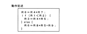
図2は、動作記述格納手段101に格納される動作記述の例を示している。動作記述は、回路の動作を表しており、例えば、C言語等により記述されているが、SystemC、SpecC、ANSI−C、それらの派生言語、System Verilog等により記述されていてもよい。図の例において、第1行目から順に実行される動作が記述されており、R1からR9はデータ(変数)を示している。図に示されるように、この動作記述では、第1行目において、R4とR7を乗算した結果をR6とし、第2行目において、R1よりR2が大きいか否か判定し、当該判定が真であれば、第3行目において、R4とR5を乗算した結果をR3とし、当該判定が偽であれば、第5行目において、R8とR5を乗算しさらにR9を加算した結果をR6とするように記述されている。以下の図3乃至図13は、図2の動作記述に基づいて、各手段の処理が行なわれ格納されたデータの例である。 FIG. 2 shows an example of the behavior description stored in the behavior description storage means 101. The operation description represents the operation of the circuit. For example, the operation description is described in C language, but may be described in SystemC, SpecC, ANSI-C, a derivative language thereof, System Verilog, or the like. In the example of the figure, operations to be executed in order from the first line are described, and R1 to R9 indicate data (variables). As shown in the figure, in this behavioral description, in the first line, the result of multiplying R4 and R7 is R6, and in the second line, it is determined whether R2 is larger than R1, and this determination is true. Then, in the third line, the result of multiplying R4 and R5 is R3, and if the determination is false, the result of multiplying R8 and R5 and further adding R9 is R6 in the fifth line. It is described to be. The following FIGS. 3 to 13 are examples of data stored by processing of each means based on the behavioral description of FIG.
図3は、図2の動作記述から生成されたデータフローグラフの例を示している。データフローグラフは、節点と枝によって構成され、枝はデータを表し、節点は演算を表しており、節点の上側に連結された枝が演算の入力枝であり、節点の下側に連結された枝が演算の出力枝である。 FIG. 3 shows an example of a data flow graph generated from the behavioral description of FIG. The data flow graph is composed of nodes and branches, where the branches represent data, the nodes represent operations, the branches connected above the nodes are the input branches of the operations, and are connected below the nodes A branch is an output branch of an operation.
図の例において、R1からR9は図2と同じデータを示し、31から35は図2の各演算を示している。C1は、R1とR2の演算32の結果(ここでは比較演算の結果)のデータである。データフローグラフは、動作合成におけるスケジューリングにより、各節点の演算がクロックサイクルに割り当てられている。この例では、状態ST1と状態ST2がそれぞれ1サイクルで実行するようにスケジューリングされている。
In the illustrated example, R1 to R9 indicate the same data as in FIG. 2, and 31 to 35 indicate the respective operations in FIG. C1 is data of the result of the
図に示されるように、このデータフローグラフでは、演算31には、R4とR7が入力され、当該演算結果がR6に出力される。すなわち、図2の第1行目に対応しており、状態ST1に割り当てられている。また、演算32には、R1とR2が入力され、演算結果がC1に出力される。すなわち、図2の第2行目に対応しており、状態ST2に割り当てられている。同様に、図2の第3行目以降も状態ST2に割り当てられている。
As shown in the figure, in this data flow graph, R4 and R7 are input to the
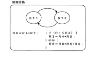
図4は、図3のデータフローグラフから生成された制御回路の例を示している。制御回路は、ステートマシンにより記述され、同じデータフローグラフから生成されるデータパスの状態遷移を表している。この例では、状態ST1において、図3の状態ST1の演算、すなわち図2の第1行目の演算を実行し、状態ST2において、図3の状態ST2の演算、すなわち図2の第2行目以降の演算を実行するように、データパスを制御する。 FIG. 4 shows an example of a control circuit generated from the data flow graph of FIG. The control circuit is described by a state machine and represents a state transition of a data path generated from the same data flow graph. In this example, in the state ST1, the calculation of the state ST1 of FIG. 3, that is, the calculation of the first row of FIG. 2 is executed, and in the state ST2, the calculation of the state ST2 of FIG. 3, that is, the second row of FIG. The data path is controlled so as to execute subsequent operations.
図5は、図3のデータフローグラフから生成されたデータパスの例を示している。データパスは、動作合成において、スケジューリングの後、アロケーションにより、演算器やレジスタが割り当てられ、さらに、演算器やレジスタを共有するためにマルチプレクサやバスが割り当てられて生成される。データパスは、データフローグラフの枝や節点に対応した回路のパスを表している。 FIG. 5 shows an example of a data path generated from the data flow graph of FIG. In the behavioral synthesis, after scheduling, a data path is assigned by an arithmetic unit and a register by allocation, and further, a multiplexer and a bus are assigned to share the arithmetic unit and the register. The data path represents a circuit path corresponding to a branch or node of the data flow graph.
この例では、R1からR9はレジスタであり、F1からF3は演算器、51から53は、マルチプレクサである。F1は図3の演算32、F2は図3の演算33及び34、F3は図3の演算35に対応している。
In this example, R1 to R9 are registers, F1 to F3 are arithmetic units, and 51 to 53 are multiplexers. F1 corresponds to the
図4で示した制御回路によって、マルチプレクサ51から53の切り替えが制御され、データパスの回路が動作する。例えば、状態ST1においては、マルチプレクサ51がR4からの入力を選択し、マルチプレクサ52がR7からの入力を選択し、マルチプレクサ53が演算器F2からの入力を選択するように切り替え、R4とR7にデータを入力すると、R6に演算結果が出力される。
Switching of the
図6は、図5のデータパスにアクティブ条件を関連付けたアクティブ条件付き回路情報の例を示している。図3のデータフローグラフと図4の制御回路の情報に基づいて、図5のデータパスの各ネットにアクティブ条件が付けてられている。 FIG. 6 shows an example of circuit information with an active condition in which an active condition is associated with the data path of FIG. Based on the data flow graph of FIG. 3 and the information of the control circuit of FIG. 4, an active condition is assigned to each net of the data path of FIG.
図において、61、62、63はネットを示している。例えば、ネット61aには、「ST2」が条件付けられており、状態ST2の場合にこのネットがアクティブになることを表している。ネット62cには、「ST2×!C1」が条件付けられている。ここで、「×」は論理積、「!C1」はC1の否定を表しており、状態ST2で、かつ、図3の演算結果C1が偽の場合に、このネットがアクティブになることを表している。ネット62bには、「ST1+ST2×C1」が条件付けられている。ここで、「+」は論理和を示しており、状態ST1の場合、または、状態ST2でかつ演算結果C1が真の場合に、このネットがアクティブになることを表している。 In the figure, reference numerals 61, 62, and 63 denote nets. For example, “ST2” is conditioned on the net 61a, which indicates that this net becomes active in the state ST2. The net 62c is conditioned on “ST2 ×! C1”. Here, “×” represents a logical product, and “! C1” represents the negation of C1, and represents that this net becomes active in the state ST2 and when the operation result C1 in FIG. 3 is false. ing. The net 62b is conditioned on “ST1 + ST2 × C1”. Here, “+” indicates a logical sum, which indicates that this net becomes active in the state ST1 or in the state ST2 and the operation result C1 is true.
図7は、図6におけるレジスタR1とレジスタR6の間のパスの例を示している。図中のパスaにおける、各ネットのアクティブ条件は、ネット61aが「ST2」、ネット62aが「ST2」、ネット63bが「ST1」であり、これらの論理積がパスaのアクティブ条件となる。状態ST2と状態ST1は、別のクロックサイクルであり、同時に動作しないため、ST1とST2の論理積は0である。したがって、パスaのアクティブ条件は、ST2×ST2×ST1=0となり、パスaはフォールスパスであると判断することができる。 FIG. 7 shows an example of a path between the register R1 and the register R6 in FIG. The active condition of each net in the path a in the figure is “ST2” for the net 61a, “ST2” for the net 62a, and “ST1” for the net 63b, and the logical product of these is the active condition for the path a. Since the state ST2 and the state ST1 are different clock cycles and do not operate at the same time, the logical product of ST1 and ST2 is 0. Therefore, the active condition of the path a is ST2 × ST2 × ST1 = 0, and it can be determined that the path a is a false path.
また、パスbにおける、各ネットのアクティブ条件は、ネット61aが「ST2」、ネット62aが「ST2」、ネット63cが「ST2×!C1」、ネット63eが「ST2×!C1」である。状態ST2において比較演算C1が動作するため、ST2とC1の論理積は0ではない。したがって、パスbのアクティブ条件は、ST2×ST2×ST2×!C1×ST2×!C1=ST2×!C1となり、パスbはトゥルーパスであると判断することができる。このように、アクティブ条件付き回路情報では、当該ネットに迂回するパスが存在する場合でも、当該ネットのみのアクティブ条件が付けられている。 The active conditions of each net in the path b are “ST2” for the net 61a, “ST2” for the net 62a, “ST2 ×! C1” for the net 63c, and “ST2 ×! C1” for the net 63e. Since the comparison operation C1 operates in the state ST2, the logical product of ST2 and C1 is not zero. Therefore, the active condition of the path b is ST2 × ST2 × ST2 ×! C1 x ST2 x! C1 = ST2 ×! C1 and the path b can be determined to be a true path. As described above, in the circuit information with active condition, even when there is a detour path in the net, the active condition only for the net is attached.
図8は、図7のアクティブ条件付き回路情報が格納される場合の具体的なデータの例である。アクティブ条件付き回路情報には、ネットと、当該ネットの入力側/出力側インスタンス、当該ネットのアクティブ条件が含まれている。例えば、ネット61aには、入力側インスタンスにR1、出力側インスタンスにF1、アクティブ条件にST2が対応付けられ、格納されている。この例では、ネットを基にして、その他のデータを対応付けているが、これに限らず、インスタンスを基にしてもよい。 FIG. 8 is an example of specific data when the circuit information with active condition of FIG. 7 is stored. The circuit information with active condition includes the net, the input / output instance of the net, and the active condition of the net. For example, in the net 61a, R1 is associated with the input instance, F1 is associated with the output instance, and ST2 is associated with the active condition and stored. In this example, other data is associated based on the net. However, the present invention is not limited to this, and may be based on an instance.
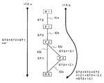
図9は、図6のアクティブ条件付き回路情報に迂回パスのアクティブ条件を付けた、迂回パス条件付き回路情報の例を示している。迂回パスのアクティブ条件は、迂回パス条件設定手段123により、ネットのアクティブ条件に加えられる。この例では、太線で示したネット63bに、迂回パスであるネット63c及び63eのアクティブ条件「ST2×!C1」を加えた「ST1+ST2×!C1」が条件付けられている。このように、ネットのアクティブ条件と迂回パスのアクティブ条件との論理和が、当該ネットのアクティブ条件となる。
FIG. 9 shows an example of circuit information with a detour path condition obtained by adding a detour path active condition to the circuit information with an active condition of FIG. The bypass path active condition is added to the net active condition by the bypass path condition setting means 123. In this example, “ST1 + ST2 ×! C1” obtained by adding the active condition “ST2 ×! C1” of the
図10は、図9におけるレジスタR1とレジスタR6の間のパスの例を示している。図7と比べて、ネット63bのアクティブ条件に迂回パスのアクティブ条件が加えられて「ST1+ST2×!C1」となり、パスaのアクティブ条件は、ST2×ST2×(ST1+ST2×!C1)=ST2×!C1となる。従って、図7と異なり、パスaは、トゥルーパスであると判断することができる。 FIG. 10 shows an example of a path between the register R1 and the register R6 in FIG. Compared to FIG. 7, the active condition of the detour path is added to the active condition of the net 63b to become “ST1 + ST2 ×! C1”, and the active condition of the path a is ST2 × ST2 × (ST1 + ST2 ×! C1) = ST2 ×! C1. Therefore, unlike FIG. 7, the path a can be determined to be a true path.
図11は、図10の迂回パス付き回路情報が格納される場合の具体的なデータの例である。迂回パス条件付き回路情報には、ネットと、当該ネットの入力側/出力側インスタンス、当該ネットの迂回パス付きアクティブ条件が含まれている。図8と比べて、アクティブ条件に迂回パスのアクティブ条件が加えられているが、それ以外は図8と同じである。 FIG. 11 is an example of specific data when the circuit information with a bypass path in FIG. 10 is stored. The circuit information with a detour path condition includes a net, an input / output instance of the net, and an active condition with a detour path of the net. Compared to FIG. 8, the active condition of the detour path is added to the active condition, but other than that is the same as FIG. 8.
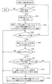
次に、図12のフローチャートを用いて、本発明の実施の形態1にかかる迂回パス条件設定処理について説明する。この処理は、迂回パス条件設定手段123における処理であり、例えば、CPU等において所定のアプリケーションプログラムにより実行される。
Next, a detour path condition setting process according to the first exemplary embodiment of the present invention will be described using the flowchart of FIG. This process is a process in the detour path
まず、回路中のネットを全て処理したかどうか判定する(S101)。アクティブ条件付き回路情報格納手段122に格納されたアクティブ条件付き回路情報中のネットの全てについて、S102以降の処理を行ったかどうか判定する。例えば、図8のデータの例では、ネット61aからネット63eの全てのネットの処理が終了したかどうか判定する。 First, it is determined whether all nets in the circuit have been processed (S101). It is determined whether or not the processing from S102 onward has been performed for all the nets in the circuit information with active condition stored in the circuit information storage means 122 with active condition. For example, in the data example of FIG. 8, it is determined whether or not the processing of all nets from the net 61a to the net 63e has been completed.
S101において、全てのネットの処理が終了したと判定した場合、迂回パス条件設定処理を終了する。 If it is determined in S101 that all nets have been processed, the detour path condition setting process ends.
S101において、処理していないネットが残っていると判定した場合、回路中のネットを1つ取り出す(S102)。アクティブ条件付き回路情報格納手段122に格納されたアクティブ条件付き回路情報中のネットの1つについて、データを読み出し、当該ネットについて、S103以降の処理を行う。すでにS103以降の処理を行ったネットがある場合には、まだ、当該処理を行っていないネットのデータを読み出す。アクティブ条件付き回路情報からネットを読み出す順序は、任意の順序でよい。
If it is determined in S101 that an unprocessed net remains, one net in the circuit is taken out (S102). Data is read out for one of the nets in the circuit information with active condition stored in the circuit information with active
例えば、図8のデータの例では、ネット63bが未処理の場合、ネット63bのデータを読み出し、ネット63bの処理が終了している場合、次のネット63cのデータを読み出す。ここでは、ネット63bのデータを読み出した例について、以下の処理を説明する。 For example, in the data example of FIG. 8, when the net 63b is not processed, the data of the net 63b is read, and when the processing of the net 63b is finished, the data of the next net 63c is read. Here, the following processing will be described with respect to an example in which data of the net 63b is read.
次いで、対象ネットの出力側インスタンスについて、そのインスタンスの入力側に接続されている全てのネットを探索パスリストに登録する(S103)。S102で読み出したネットのデータから、当該ネットの出力側に接続されているインスタンスを参照する。そして、アクティブ条件付き回路情報から、当該インスタンスの入力側に接続されている全てのネットを取得する。その後、取得した全てのネットを探索パスリストに登録する。 Next, for the output side instance of the target net, all nets connected to the input side of the instance are registered in the search path list (S103). The instance connected to the output side of the net is referred to from the net data read in S102. Then, all nets connected to the input side of the instance are acquired from the circuit information with active condition. Thereafter, all acquired nets are registered in the search path list.
尚、この例では、インスタンスの入力側にネットを連結しながら迂回パスを探索するが、これに限らず、反対の方向に探索、すなわち、対象ネットの入力側のインスタンスについて、その出力側にネットを連結しながら迂回パスを探索してもよい。 In this example, the bypass path is searched while connecting the net to the input side of the instance. However, the search is not limited to this, and the search is performed in the opposite direction. The detour path may be searched while connecting the two.
例えば、S102で読み出したネット63bのデータより、出力側のインスタンスはR6である。このR6の入力側に接続されているネットは、図8のアクティブ条件付き回路情報の例では、63bと63eである。ネット63bは、当該処理中のネットであるので、対象外とし、ここでは、ネット63eのみからなるパスであるパス63eを探索パスリストに登録する。探索パスリストにおいては、1つのネットのみであってもパスとする。このときの、探索パスリストのデータの例を図13(a)に示す。図に示されるように、探索パスリストは、当該処理で探索する探索パスと、当該探索パスの入力側/出力側インスタンスと、当該探索パスのアクティブ条件を含んでいる。このように、探索パスリストには、1つ以上のネットが登録され、この探索パスについて、S104以降の処理を行う。
For example, the output instance is R6 from the data of the net 63b read in S102. The nets connected to the input side of R6 are 63b and 63e in the example of the circuit information with active condition of FIG. Since the net 63b is a net being processed, the net 63b is excluded, and here, the
次いで、探索パスリストが空かどうか判定する(S104)。S103で登録された探索パスリスト中のパスの全てについて、S105以降の処理を行ったかどうかを、探索パスリストに登録されているパスの有無により判定する。例えば、図13(a)のデータの例では、パス63eが登録されているので、S105以降の処理を行う。
Next, it is determined whether the search path list is empty (S104). Whether all the paths in the search path list registered in S103 have been processed in S105 or later is determined based on the presence or absence of a path registered in the search path list. For example, in the example of the data in FIG. 13A, since the
S104において、探索パスリストが空であると判断した場合、再度、S101を実行し、次のネットの処理を行う。また、このとき、処理が終了したネットのデータを、迂回パス付き回路情報格納手段124に格納してもよい。
If it is determined in S104 that the search path list is empty, S101 is executed again to process the next net. At this time, the net data for which processing has been completed may be stored in the circuit
S104において、探索パスリストが空ではないと判断された場合、探索パスリスト中の任意のパスを取り出す(S105)。S103で登録した探索パスリスト中の探索パスの1つについて、データを読み出し、当該探索パスについて、S106以降の処理を行う。このとき、読み出したパスのデータを探索パスリストから削除する。例えば、図13(a)のデータの例では、パス63eのデータを読み出し、パス63eのデータを探索パスリストから削除する。ここでは、パス63eのデータを読み出した例について、以下の処理を説明する。
If it is determined in S104 that the search path list is not empty, an arbitrary path in the search path list is extracted (S105). Data is read for one of the search paths in the search path list registered in S103, and the processes after S106 are performed for the search path. At this time, the read path data is deleted from the search path list. For example, in the example of the data in FIG. 13A, the data of the
次いで、対象パスがアクティブかどうか判定する(S106)。S105で読み出した探索パスのデータから、当該探索パスのアクティブ条件を参照し、当該探索パスがトゥルーパスかあるいはフォールスパスかどうか判定する。例えば、S105で読み出したパス63eのデータより、アクティブ条件は「ST2×!C1」である。したがって、パス63eのパスは、トゥルーパスであると判定される。
Next, it is determined whether the target path is active (S106). From the search path data read out in S105, the active condition of the search path is referred to and it is determined whether the search path is a true path or a false path. For example, from the data of the
S106において、対象パスがフォールスパスと判断された場合、再度、S104を実行し、探索パスリストに登録されているパスについて処理を行う。 If it is determined in S106 that the target path is a false path, S104 is executed again to process the paths registered in the search path list.
S106において、対象パスがトゥルーパスと判断された場合、さらに、対象パスの先頭インスタンスが対象ネットの入力側インスタンスと同一かどうか判定する(S107)。S105で読み出した探索パスのデータから、当該探索パスの入力側(先頭)に接続されているインスタンスを参照する。そして、当該探索パスの入力側インスタンスと、S102で読み出したネットの入力側のインスタンスを比較し、同一かどうか判定する。 If it is determined in S106 that the target path is a true path, it is further determined whether or not the first instance of the target path is the same as the input side instance of the target net (S107). The instance connected to the input side (first) of the search path is referred to from the search path data read in S105. Then, the input side instance of the search path is compared with the input side instance of the net read in S102 to determine whether or not they are the same.
例えば、S105で読み出したパス63eのデータより、入力側のインスタンスはF3である。また、S102で読み出したネット63bの入力側インスタンスはF2である。したがって、探索パスのネット63eの入力側インスタンスと、探索パスの処理中であるネット63eの入力側インスタンスは同一ではないと判定される。
For example, the instance on the input side is F3 from the data of the
S107において、対象パスの先頭インスタンスが対象ネットの入力側インスタンスと同一ではないと判定された場合、当該パスを迂回パスではないとして、対象パスとその入力側に接続されている各ネットとで構成されるパスを探索パスリストに登録する(S109)。その後、再度、S104を実行し、次のパスについて処理を行う。 If it is determined in S107 that the first instance of the target path is not the same as the input side instance of the target net, the target path and each net connected to the input side are configured assuming that the path is not a detour path The registered path is registered in the search path list (S109). Thereafter, S104 is executed again, and processing is performed for the next pass.
すなわち、S105で読み出した探索パスのデータから、当該探索パスの入力側に接続されているインスタンスを参照する。そして、アクティブ条件付き回路情報から、当該インスタンスの入力側に接続されている全てのネットを取得する。その後、当該探索パスと取得した全てのネットにより構成されるパスを新たに生成し、当該新たなパスを探索パスリストに登録する。 In other words, the instance connected to the input side of the search path is referred to from the search path data read in S105. Then, all nets connected to the input side of the instance are acquired from the circuit information with active condition. Thereafter, a new path composed of the search path and all acquired nets is newly generated, and the new path is registered in the search path list.
例えば、S105で読み出したパス63eのデータより、入力側のインスタンスはF3である。このF3の入力側に接続されているネットは、図8のアクティブ条件付き回路情報の例では、ネット63cとネット63dである。したがって、ネット63cとネット63eから構成されるパスであるパス63c−63eと、ネット63dとネット63eから構成されるパスであるパス63d−63eを探索パスリストに登録する。このときの探索パスリストのデータの例を図13(b)に示す。その後、登録したパス63c−63e、パス63d−63eについて、S104から処理が行われる。
For example, the instance on the input side is F3 from the data of the
S107において、対象パスの先頭インスタンスが対象ネットの入力側インスタンスと同一と判定された場合、当該パスが迂回パスであるとして、対象パスのアクティブ条件を対象ネットのアクティブ条件に追加する(S108)。 If it is determined in S107 that the first instance of the target path is the same as the input-side instance of the target net, the target path active condition is added to the target net active condition, assuming that the path is a bypass path (S108).
すなわち、S105で読み出した探索パスのデータから、当該探索パスのアクティブ条件を参照する。そして、当該アクティブ条件をS102で読み出したネットのアクティブ条件に論理和で、追加する。 That is, the search path active condition is referred to from the search path data read in S105. Then, the active condition is added as a logical sum to the active condition of the net read in S102.
例えば、図13(b)のパス63c−63eのデータを処理する場合、当該データの入力側インスタンスは、F2であるから、S102で読み出したネット63bの入力側インスタンスと同一である。したがって、パス63c−63eのアクティブ条件「ST2×!C1」を、ネット63bのアクティブ条件「ST1」に論理和で加える。すなわち、ネット63bのアクティブ条件は、図11に示すように、「ST1+ST2×!C1」となる。
For example, when processing the data of the
このようにして、アクティブ条件が付けられたデータパスのネットについて、当該ネットの迂回パスのアクティブ条件をさらに加えることができる。 In this way, the active condition of the detour path of the net can be further added to the net of the data path to which the active condition is attached.
このような構成により、動作合成されたデータパスの中からフォールスパスを抽出し、インスタンス指定のフォールスパスを出力することができる。特に、それぞれのネットに迂回パスが存在する場合には、迂回パスのアクティブ条件も当該ネットのアクティブ条件に加えることにより、フォールスパスをインスタンス指定しても、トゥルーパスを含むことはなくなる。すなわち、インスタンス指定で対象となるすべてのパスがフォールスパスであることを保証できるため、フォールスパスを正確に指定することが可能となる。したがって、ネットリスト生成ツールや配置配線ツール、静的タイミング解析ツールに対してフォールスパスを正確に指定することができ、不要なタイミング検証、最適化等を行うことがなくなり、設計作業の効率を向上することができる。 With such a configuration, it is possible to extract a false path from a behaviorally synthesized data path and output an instance-specified false path. In particular, when a detour path exists in each net, the true condition is not included even if the false path is specified as an instance by adding the active condition of the detour path to the active condition of the net. In other words, since it is possible to ensure that all the paths targeted by the instance designation are false paths, the false paths can be designated accurately. Therefore, the false path can be accurately specified for the netlist generation tool, place-and-route tool, and static timing analysis tool, eliminating unnecessary timing verification and optimization and improving the efficiency of design work. can do.
発明の実施の形態2.
次に、図14を用いて、本発明の実施の形態2にかかる回路設計支援システムの構成について説明する。この回路設計支援システム1は、図1と同様のシステムであり、図1と同様の方法で抽出したフォールスパスに基づいて、ネットリストの生成や静的タイミング解析を行い、さらに、静的タイミング解析の結果得られる遅延レポートから不要なフォールスパスを除去する処理を実行するシステムである。
Next, the configuration of the circuit design support system according to the second exemplary embodiment of the present invention will be described with reference to FIG. This circuit
図に示されるように、回路設計支援システム1は、回路設計支援手段100、入力手段110、表示手段111を備えている。回路設計支援手段100は、図1の構成に加えて、ネットリスト生成手段105、ネットリスト情報格納手段106、静的タイミング解析手段107、クリティカルパス情報格納手段108、フォールスパス除去手段109、RTL回路情報格納手段110、合成情報格納手段111を備えている。
As shown in the figure, the circuit
本実施形態の動作合成手段102は、図1のフォールスパス抽出手段120を含んでいる。RTL回路情報格納手段110には、図1の動作合成回路情報格納手段103に含まれるRTL回路が格納されている。合成情報格納手段111には、図1の動作合成回路情報格納手段103と同様の回路情報が格納されている。
The behavioral synthesis means 102 of this embodiment includes the false path extraction means 120 of FIG. The RTL circuit
ネットリスト生成手段105は、動作合成回路情報格納手段103に格納されたRTL回路を論理合成することにより、静的タイミング解析可能なネットリストを生成し、ネットリスト情報格納手段106に格納する。このとき、ネットリスト生成手段105は、フォールスパス情報格納手段104に格納されたインスタンス指定のフォールスパスに対応する回路の最適化を実施しなくてもよい。これにより、論理合成処理にかかる時間を短縮することができる。
The net
尚、ネットリスト生成手段105は、表示手段111等に出力してもよいし、その他の装置に、ネットリストを出力してもよい。
The net
静的タイミング解析手段107は、ネットリスト情報格納手段106に格納されたネットリストから静的なタイミング特性を解析してタイミング検証を行い、遅延制約を満たしていないパスであるクリティカルパス(遅延パスともいう)を抽出し、複数のクリティカルパスを含む遅延レポートをクリティカルパス情報格納手段108に格納する。このとき、静的タイミング解析手段107は、フォールスパス情報格納手段104に格納されたインスタンス指定のフォールスパスについては、タイミング検証を行わなくてもよい。また、フォールスパスについては、遅延違反した場合でも、クリティカルパスとして出力しなくてもよい。
The static
フォールスパス除去手段109は、クリティカルパス情報格納手段108に格納されているクリティカルパスを解析し、当該クリティカルパスに含まれるフォールスパスを除去し、フォールスパスを除去したクリティカルパスを表示手段111に出力する。
The false
フォールスパス除去手段109は、クリティカルパス情報格納手段108に格納されている全てのクリティカルパスについて処理を行う。まず、クリティカルパス情報格納手段108に格納されているクリティカルパスを読み出す。次いで、当該クリティカルパスがフォールスパスかどうか判定する。例えば、当該クリティカルパスを構成する各ネットのアクティブ条件を合成情報格納手段111から取得し、各ネットのアクティブ条件の論理積により、フォールスパスかどうか判定する。当該クリティカルパスがフォールスパスの場合、当該クリティカルパスをクリティカルパス情報格納手段108から削除する。フォールスパスに該当する全てのクリティカルパスをクリティカルパス情報格納手段108から削除した後、当該クリティカルパス情報格納手段108を表示手段111に出力する。尚、クリティカルパス情報格納手段108のデータを直接削除せずに、表示手段111にのみフォールスパスを削除したデータを出力してもよい。
The false
尚、ここでは、動作合成回路情報格納手段103と同様の回路情報を含む合成情報格納手段111の情報に基づいて、クリティカルパスからフォールスパスを除去しているが、その他の情報に基づいてフォールスパスを除去してもよい。例えば、図1で示した、アクティブ条件付き回路情報格納手段122や迂回パス条件付き回路情報格納手段124の情報に基づいて同様に、クリティカルパスからフォールスパスを除去してもよい。
Here, the false path is removed from the critical path based on the information of the synthesis information storage means 111 including the same circuit information as the behavioral synthesis circuit information storage means 103, but the false path is based on other information. May be removed. For example, the false path may be similarly removed from the critical path based on the information in the circuit
このような構成により、フォールスパス情報格納手段104に全てのフォールスパスが含まれない場合であっても、動作合成手段やフォールスパス抽出手段が出力する情報に基づいて、フォールスパスに対応するクリティカルパスを検出し、当該クリティカルパスを遅延レポートから除去することができる。すなわち、フォールスパスを含まない遅延レポートを生成することができ、遅延レポートの精度を向上することができる。
With such a configuration, even if the false path
その他の発明の実施の形態.
上述した回路設計支援システム1を実現するためのハードウェア構成の例を図15に示す。回路設計支援システム1は、典型的なコンピュータ・システムが利用可能であり、中央処理装置(CPU)201とメモリ204とを含んでいる。
Other Embodiments of the Invention
An example of a hardware configuration for realizing the circuit
CPU201とメモリ204とは、バスを介して補助記憶装置としてのハードディスク装置213に接続される。フレキシブルディスク装置220、ハードディスク装置213・230、CD−ROMドライブ226・229、MOドライブ228等の記憶媒体駆動装置は、フレキシブルディスク・コントローラ219、IDEコントローラ225、SCSIコントローラ227等の各種コントローラを介してバスに接続される。フレキシブルディスク装置220等の記憶媒体駆動装置には、フレキシブルディスク等の可搬型記憶媒体が挿入される。
The
記憶媒体にはオペレーティングシステムと共同してCPU201等に命令を与え、回路設計支援システム1の機能を実施するためのコンピュータ・プログラムを記憶することができる。コンピュータ・プログラムは、メモリ204にロードされることによって実行される。コンピュータ・プログラムは圧縮し、又、複数に分割して記憶媒体に記憶することができる。ハードウェア構成は、典型的には、ユーザ・インターフェース・ハードウェアを備える。
The storage medium can store a computer program for executing a function of the circuit
ユーザ・インターフェース・ハードウェアとしては、例えば、入力をするためのポインティングデバイス(マウス207、ジョイスティック等)やキーボード206、あるいは、視覚データをユーザに提示するための液晶ディスプレイなどの表示装置211やCRTディスプレイ212がある。
Examples of user interface hardware include a
また、パラレルポート216を介してプリンタを接続するも可能である。このコンピュータ・システムは、シリアルポート215を介してモデムを接続することが可能であり、シリアルポート215およびモデムまたはトークンリングや通信アダプタ218等を介してネットワークに接続し、他のコンピュータ・システムと通信を行っている。尚、上記構成は必要に応じて省略することができる。
It is also possible to connect a printer via the
1 回路設計支援システム
101 動作記述格納手段
102 動作合成手段
103 動作合成回路情報格納手段
104 フォールスパス情報格納手段
120 フォールスパス抽出手段
121 アクティブ条件設定手段
122 アクティブ条件付き回路情報格納手段
123 迂回パス条件設定手段
124 迂回パス条件付き回路情報格納手段
125 フォールスパス探索手段
126 アクティブ情報格納手段
DESCRIPTION OF
Claims (10)
動作合成により生成された回路情報と、前記回路情報に対応するデータパスとを取得するステップと、
前記回路情報に基づき、前記データパスに含まれる複数の転送路のそれぞれについて、当該転送路にデータが転送される条件であるアクティブ条件を決定するステップと、
前記転送路のアクティブ条件に基づき、前記複数の転送路のそれぞれについて、当該転送路を迂回してデータを転送する迂回パスのアクティブ条件を決定するステップと、
前記転送路のアクティブ条件と前記迂回パスのアクティブ条件とに基づき、前記転送路と当該転送路の迂回パスから構成される迂回データパスのアクティブ条件を決定するステップと、
前記転送路のアクティブ条件と前記迂回データパスのアクティブ条件に基づき、前記データパスに含まれる複数のパスのそれぞれについて、アクティブ条件を決定するステップと、
前記パスのアクティブ条件に基づき、フォールスパスを検出するステップと、
を備えるプログラム。 A program for causing a computer to execute processing for detecting a false path from among data paths having a plurality of paths including a plurality of transfer paths, wherein the processing includes:
Obtaining circuit information generated by behavioral synthesis and a data path corresponding to the circuit information;
Based on the circuit information, for each of a plurality of transfer paths included in the data path, determining an active condition that is a condition for transferring data to the transfer path;
Determining, based on the active condition of the transfer path, for each of the plurality of transfer paths, an active condition of a bypass path that bypasses the transfer path and transfers data;
Determining an active condition of a bypass data path composed of the transfer path and a bypass path of the transfer path based on an active condition of the transfer path and an active condition of the bypass path;
Determining an active condition for each of a plurality of paths included in the data path based on an active condition of the transfer path and an active condition of the bypass data path;
Detecting a false path based on an active condition of the path;
A program comprising
前記転送路のアクティブ条件を決定するステップは、前記データパスと前記素子割り当て情報により対応付けられた、データフローグラフの状態により、当該転送路のアクティブ条件を決定する、
請求項1に記載のプログラム。 The circuit information includes a data flow graph and element allocation information,
The step of determining the active condition of the transfer path determines the active condition of the transfer path according to the state of the data flow graph associated with the data path and the element allocation information.
The program according to claim 1.
前記複数の転送路のそれぞれについて、当該転送路の入力側の素子と出力側の素子を含むパスを前記データパスから検索し、当該転送路の迂回パスを決定するステップと、
前記迂回パスに含まれる転送路のアクティブ条件に基づいて、前記迂回パスのアクティブ条件を決定するステップと、
を備える、請求項1又は2に記載のプログラム。 Determining an active condition of the bypass path,
For each of the plurality of transfer paths, searching the data path for a path including an input side element and an output side element of the transfer path, and determining a detour path of the transfer path;
Determining an active condition of the bypass path based on an active condition of a transfer path included in the bypass path;
The program according to claim 1, comprising:
前記迂回データパスのアクティブ条件は、当該迂回データパスに含まれる転送路のアクティブ条件と、当該迂回データパスに含まれる迂回パスのアクティブ条件との論理和であり、
前記パスのアクティブ条件は、当該パスに含まれる複数の転送路のアクティブ条件と、当該パスに含まれる複数の迂回データパスのアクティブ条件とのそれぞれの論理積であり、
前記フォールスパスを検出するステップは、前記パスのアクティブ条件の論理演算が0の場合に、当該パスをフォールスパスと決定する、
請求項1乃至3のいずれかに記載のプログラム。 The active condition of the detour path is a logical product of the active conditions of a plurality of transfer paths included in the detour path,
The active condition of the detour data path is a logical sum of the active condition of the transfer path included in the detour data path and the active condition of the detour path included in the detour data path,
The active condition of the path is a logical product of an active condition of a plurality of transfer paths included in the path and an active condition of a plurality of detour data paths included in the path,
The step of detecting the false path determines the path as a false path when the logical operation of the active condition of the path is 0.
The program according to any one of claims 1 to 3.
請求項1乃至4のいずれかに記載のプログラム。 Outputting the detected false path by a plurality of instances included in the false path;
The program according to any one of claims 1 to 4.
動作合成により生成された回路情報と、前記回路情報からタイミング検証により生成された遅延情報とを取得するステップと、
前記回路情報に基づき、前記遅延情報に含まれる複数のクリティカルパスのそれぞれについて、当該クリティカルパスにデータが転送される条件であるアクティブ条件を決定するステップと、
前記アクティブ条件に基づいて、前記クリティカルパスがフォールスパスかどうか判定するステップと、
前記クリティカルパスがフォールスパスの場合、前記遅延情報から当該クリティカルパスを除去するステップと、
を備えるプログラム。 A program that causes a computer to execute a process of removing a false path from delay information including a plurality of critical paths,
Acquiring circuit information generated by behavioral synthesis and delay information generated by timing verification from the circuit information;
Based on the circuit information, for each of a plurality of critical paths included in the delay information, determining an active condition that is a condition for transferring data to the critical path;
Determining whether the critical path is a false path based on the active condition;
If the critical path is a false path, removing the critical path from the delay information;
A program comprising
動作合成により生成された回路情報と、前記回路情報に対応するデータパスとを取得するステップと、
前記回路情報に基づき、前記データパスに含まれる複数の転送路のそれぞれについて、当該転送路にデータが転送される条件であるアクティブ条件を決定するステップと、
前記転送路のアクティブ条件に基づき、前記複数の転送路のそれぞれについて、当該転送路を迂回してデータを転送する迂回パスのアクティブ条件を決定するステップと、
前記転送路のアクティブ条件と前記迂回パスのアクティブ条件とに基づき、前記転送路と当該転送路の迂回パスから構成される迂回データパスのアクティブ条件を決定するステップと、
前記転送路のアクティブ条件と前記迂回データパスのアクティブ条件に基づき、前記データパスに含まれる複数のパスのそれぞれについて、アクティブ条件を決定するステップと、
前記パスのアクティブ条件に基づき、フォールスパスを検出するステップと、
を備える設計方法。 A design method for detecting a false path from data paths having a plurality of paths including a plurality of transfer paths,
Obtaining circuit information generated by behavioral synthesis and a data path corresponding to the circuit information;
Based on the circuit information, for each of a plurality of transfer paths included in the data path, determining an active condition that is a condition for transferring data to the transfer path;
Determining, based on the active condition of the transfer path, for each of the plurality of transfer paths, an active condition of a bypass path that bypasses the transfer path and transfers data;
Determining an active condition of a bypass data path composed of the transfer path and a bypass path of the transfer path based on an active condition of the transfer path and an active condition of the bypass path;
Determining an active condition for each of a plurality of paths included in the data path based on an active condition of the transfer path and an active condition of the bypass data path;
Detecting a false path based on an active condition of the path;
A design method comprising:
動作合成により生成された回路情報と、前記回路情報からタイミング検証により生成された遅延情報とを取得するステップと、
前記回路情報に基づき、前記遅延情報に含まれる複数のクリティカルパスのそれぞれについて、当該クリティカルパスにデータが転送される条件であるアクティブ条件を決定するステップと、
前記アクティブ条件に基づいて、前記クリティカルパスがフォールスパスかどうか判定するステップと、
前記クリティカルパスがフォールスパスの場合、前記遅延情報から当該クリティカルパスを除去するステップと、
を備える設計方法。 A design method for removing a false path from delay information including a plurality of critical paths,
Acquiring circuit information generated by behavioral synthesis and delay information generated by timing verification from the circuit information;
Based on the circuit information, for each of a plurality of critical paths included in the delay information, determining an active condition that is a condition for transferring data to the critical path;
Determining whether the critical path is a false path based on the active condition;
If the critical path is a false path, removing the critical path from the delay information;
A design method comprising:
動作合成により生成された回路情報と、前記回路情報に対応するデータパスとを取得する手段と、
前記回路情報に基づき、前記データパスに含まれる複数の転送路のそれぞれについて、当該転送路にデータが転送される条件であるアクティブ条件を決定する手段と、
前記転送路のアクティブ条件に基づき、前記複数の転送路のそれぞれについて、当該転送路を迂回してデータを転送する迂回パスのアクティブ条件を決定する手段と、
前記転送路のアクティブ条件と前記迂回パスのアクティブ条件とに基づき、前記転送路と当該転送路の迂回パスから構成される迂回データパスのアクティブ条件を決定する手段と、
前記転送路のアクティブ条件と前記迂回データパスのアクティブ条件に基づき、前記データパスに含まれる複数のパスのそれぞれについて、アクティブ条件を決定する手段と、
前記パスのアクティブ条件に基づき、フォールスパスを検出する手段と、
を備える回路設計支援システム。 A circuit design support system for detecting a false path from data paths having a plurality of paths including a plurality of transfer paths,
Means for acquiring circuit information generated by behavioral synthesis and a data path corresponding to the circuit information;
Based on the circuit information, for each of a plurality of transfer paths included in the data path, a means for determining an active condition that is a condition for transferring data to the transfer path;
Means for determining an active condition of a detour path for detouring the transfer path and transferring data for each of the plurality of transfer paths based on the active condition of the transfer path;
Means for determining an active condition of a bypass data path composed of the transfer path and a bypass path of the transfer path based on an active condition of the transfer path and an active condition of the bypass path;
Means for determining an active condition for each of a plurality of paths included in the data path based on an active condition of the transfer path and an active condition of the bypass data path;
Means for detecting a false path based on an active condition of the path;
A circuit design support system comprising:
動作合成により生成された回路情報と、前記回路情報からタイミング検証により生成された遅延情報とを取得する手段と、
前記回路情報に基づき、前記遅延情報に含まれる複数のクリティカルパスのそれぞれについて、当該クリティカルパスにデータが転送される条件であるアクティブ条件を決定する手段と、
前記アクティブ条件に基づいて、前記クリティカルパスがフォールスパスかどうか判定する手段と、
前記クリティカルパスがフォールスパスの場合、前記遅延情報から当該クリティカルパスを除去する手段と、
を備える回路設計支援システム。
A circuit design support system for removing a false path from delay information including a plurality of critical paths,
Means for acquiring circuit information generated by behavioral synthesis and delay information generated by timing verification from the circuit information;
Based on the circuit information, for each of a plurality of critical paths included in the delay information, a means for determining an active condition that is a condition for transferring data to the critical path;
Means for determining whether the critical path is a false path based on the active condition;
If the critical path is a false path, means for removing the critical path from the delay information;
A circuit design support system comprising:
Priority Applications (3)
| Application Number | Priority Date | Filing Date | Title |
|---|---|---|---|
| JP2004108988A JP2005293349A (en) | 2004-04-01 | 2004-04-01 | Circuit design support system, design method and program |
| DE102005014712A DE102005014712A1 (en) | 2004-04-01 | 2005-03-31 | Circuit Development Auxiliary System, Circuit Development Method and Program Product for Circuit Development |
| US11/094,315 US20050223345A1 (en) | 2004-04-01 | 2005-03-31 | Circuit design assistant system, circuit design method, and program product for circuit design |
Applications Claiming Priority (1)
| Application Number | Priority Date | Filing Date | Title |
|---|---|---|---|
| JP2004108988A JP2005293349A (en) | 2004-04-01 | 2004-04-01 | Circuit design support system, design method and program |
Publications (1)
| Publication Number | Publication Date |
|---|---|
| JP2005293349A true JP2005293349A (en) | 2005-10-20 |
Family
ID=35055821
Family Applications (1)
| Application Number | Title | Priority Date | Filing Date |
|---|---|---|---|
| JP2004108988A Withdrawn JP2005293349A (en) | 2004-04-01 | 2004-04-01 | Circuit design support system, design method and program |
Country Status (3)
| Country | Link |
|---|---|
| US (1) | US20050223345A1 (en) |
| JP (1) | JP2005293349A (en) |
| DE (1) | DE102005014712A1 (en) |
Cited By (1)
| Publication number | Priority date | Publication date | Assignee | Title |
|---|---|---|---|---|
| JP2007233840A (en) * | 2006-03-02 | 2007-09-13 | Fujitsu Ltd | False path description information generating program, recording medium recording the program, false path description information generating apparatus, and false path description information generating method |
Families Citing this family (5)
| Publication number | Priority date | Publication date | Assignee | Title |
|---|---|---|---|---|
| JP2007017179A (en) * | 2005-07-05 | 2007-01-25 | Matsushita Electric Ind Co Ltd | Verification method and inspection method of semiconductor integrated circuit |
| TW200725415A (en) * | 2005-12-30 | 2007-07-01 | Tatung Co Ltd | Method for automatically translating high level programming language into hardware description language |
| US7657855B1 (en) * | 2007-05-25 | 2010-02-02 | Xilinx, Inc. | Efficient timing graph update for dynamic netlist changes |
| JP5541011B2 (en) * | 2010-09-01 | 2014-07-09 | 富士通株式会社 | Optimized netlist creation program, optimized netlist creation device, and optimized netlist creation method |
| US10331826B2 (en) | 2017-04-20 | 2019-06-25 | Texas Instruments Incorporated | False path timing exception handler circuit |
Family Cites Families (3)
| Publication number | Priority date | Publication date | Assignee | Title |
|---|---|---|---|---|
| DE69533567T2 (en) * | 1994-08-09 | 2005-11-24 | Sun Microsystems, Inc., Mountain View | Apparatus and method for detecting false timing paths in digital circuits |
| US5638290A (en) * | 1995-04-06 | 1997-06-10 | Vlsi Technology, Inc. | Method for eliminating a false critical path in a logic circuit |
| JP4549571B2 (en) * | 2001-05-16 | 2010-09-22 | ルネサスエレクトロニクス株式会社 | False path detection device, false path detection method and program thereof |
-
2004
- 2004-04-01 JP JP2004108988A patent/JP2005293349A/en not_active Withdrawn
-
2005
- 2005-03-31 DE DE102005014712A patent/DE102005014712A1/en not_active Withdrawn
- 2005-03-31 US US11/094,315 patent/US20050223345A1/en not_active Abandoned
Cited By (1)
| Publication number | Priority date | Publication date | Assignee | Title |
|---|---|---|---|---|
| JP2007233840A (en) * | 2006-03-02 | 2007-09-13 | Fujitsu Ltd | False path description information generating program, recording medium recording the program, false path description information generating apparatus, and false path description information generating method |
Also Published As
| Publication number | Publication date |
|---|---|
| DE102005014712A1 (en) | 2005-11-10 |
| US20050223345A1 (en) | 2005-10-06 |
Similar Documents
| Publication | Publication Date | Title |
|---|---|---|
| US8686753B1 (en) | Partial reconfiguration and in-system debugging | |
| JP2010079737A (en) | Timing analysis support device | |
| US6851102B2 (en) | Method and program for supporting register-transfer-level design of semiconductor integrated circuit | |
| US20080059923A1 (en) | Lsi power consumption calculation method and calculation program | |
| JP3662149B2 (en) | Repeater cell placement method, placement device, and recording medium | |
| JP5063511B2 (en) | Method and system for efficiently utilizing a multi-source network of control logic to achieve timing closure in a clock-driven logic circuit | |
| US7464361B2 (en) | System and method for asynchronous logic synthesis from high-level synchronous descriptions | |
| JP2005293349A (en) | Circuit design support system, design method and program | |
| US9965581B1 (en) | Fanout optimization to facilitate timing improvement in circuit designs | |
| JP2005242812A (en) | Circuit design support system, circuit design support method, and program | |
| US6532584B1 (en) | Circuit synthesis method | |
| JP2012174226A (en) | Layout design method of semiconductor integrated circuit | |
| US7962877B2 (en) | Port assignment in hierarchical designs by abstracting macro logic | |
| JP6091140B2 (en) | Information processing apparatus, information processing method, and program | |
| US10726182B1 (en) | Operator aware finite state machine for circuit design simulation | |
| US8024681B2 (en) | Hierarchical HDL processing method and non-transitory computer-readable storage medium | |
| JP2007004563A (en) | Library creating device, library creation program and library creating method | |
| CN1656486A (en) | Integrated circuit design method | |
| JP4901702B2 (en) | Circuit design method | |
| US20240202423A1 (en) | Runtime efficient multi-stage router flow for circuit designs | |
| JP5849973B2 (en) | Data processing apparatus, data processing system, data processing method, and data processing program | |
| JP4448048B2 (en) | Structural analysis program | |
| Corre et al. | HLS-based Fast Design Space Exploration of ad hoc hardware accelerators: a key tool for MPSoC Synthesis on FPGA | |
| JP2010146359A (en) | System, method and program for behavioral synthesis | |
| JP2000113019A (en) | Circuit designing method and design supporting device |
Legal Events
| Date | Code | Title | Description |
|---|---|---|---|
| A621 | Written request for application examination |
Free format text: JAPANESE INTERMEDIATE CODE: A621 Effective date: 20070110 |
|
| A761 | Written withdrawal of application |
Free format text: JAPANESE INTERMEDIATE CODE: A761 Effective date: 20070507 |