JP2005292843A - Optical transmission device and optical pulse tester - Google Patents
Optical transmission device and optical pulse tester Download PDFInfo
- Publication number
- JP2005292843A JP2005292843A JP2005115228A JP2005115228A JP2005292843A JP 2005292843 A JP2005292843 A JP 2005292843A JP 2005115228 A JP2005115228 A JP 2005115228A JP 2005115228 A JP2005115228 A JP 2005115228A JP 2005292843 A JP2005292843 A JP 2005292843A
- Authority
- JP
- Japan
- Prior art keywords
- optical
- optical waveguide
- optical fiber
- light
- photodetector
- Prior art date
- Legal status (The legal status is an assumption and is not a legal conclusion. Google has not performed a legal analysis and makes no representation as to the accuracy of the status listed.)
- Withdrawn
Links
Images


Landscapes
- Testing Of Optical Devices Or Fibers (AREA)
- Optical Couplings Of Light Guides (AREA)
- Optical Integrated Circuits (AREA)
Abstract
【課題】
光ファイバからの受信光を効率良く光検出器に導くことのできる双方向伝送用の光分岐結合器を提供する。
【解決手段】
光ファイバ接合部44から検出器結合用光導波路部40と分岐結合用光ファイバ80の二つに分岐され、検出器結合用光導波路部40の断面積が、光ファイバ接合部44から光検出器12の方向に向けて減少するテーパ形状をなしており、分岐結合用光ファイバ80は、光ファイバ接合部44の端面に対して概ね垂直に設ける。
【選択図】図1
【Task】
An optical branching coupler for bidirectional transmission capable of efficiently guiding received light from an optical fiber to a photodetector.
[Solution]
The optical fiber junction 44 is branched into two, a detector coupling optical waveguide 40 and a branch coupling optical fiber 80. The cross-sectional area of the detector coupling optical waveguide 40 is changed from the optical fiber junction 44 to the photodetector. The optical fiber 80 for branching and coupling is provided substantially perpendicularly to the end face of the optical fiber joint 44.
[Selection] Figure 1
Description
本発明は、光分岐結合器,光伝送装置及び光パルス試験機に関し、特に光ファイバを用いた双方向通信において光を合波・分離するための光分岐結合器及びこの光分岐結合器を用いた光伝送装置・光パルス試験機に関する。 The present invention relates to an optical branching coupler, an optical transmission device, and an optical pulse tester, and more particularly, to an optical branching coupler for multiplexing and separating light in two-way communication using an optical fiber, and the optical branching coupler. The present invention relates to optical transmission equipment and optical pulse testing machines.
特許文献1に、光を結合する方向に従って絞られるテーパ形状及びストレート形状を有しており、且つ光を分岐する伝送路の光出射端面がレンズ形状を有する合成樹脂光分岐結合器が開示されている。
また、光分岐結合器を用いて光の入出力を行い、1本の光ファイバを用いて双方向の通信を行う双方向データリンクがある。この種の装置として関連するものには例えば、非特許文献1が挙げられる。
In addition, there is a bidirectional data link that inputs and outputs light using an optical branching coupler and performs bidirectional communication using one optical fiber. For example, Non-Patent
さらには、非特許文献2に、光結合分離素子に偏光ビームスプリッタ、光源に波長532
nmのQスイッチYAGレーザを用い、プラスチック光ファイバ(以下POF)の伝送損失を測定する光パルス試験機が発表されている。
Furthermore, Non-Patent
An optical pulse tester that measures the transmission loss of a plastic optical fiber (hereinafter POF) using a Q-switched YAG laser of nm has been announced.
従来の光分岐結合器はテーパ形状の導波部端面を発光素子との結合部とし、発光素子から光分岐結合器に入射した光が絞られるようにテーパを設けている。テーパ形状において絞られた側でストレート形状の導波部と接合している。しかし、従来の光分岐結合器のようにテーパ形状を用いて光を絞った場合、光がテーパ部で反射するごとにコアとクラッドとの界面への入射角が大きくなるため、臨界角を超えた光がコアから漏れ出して損失が生じる。また、受光側の光導波路部の断面形状が光検出器の光検出部よりも大きい場合、光検出部に入射する光量が少なくなってしまう。従来の光分岐結合器では、光出射端面がレンズ形状を有しており光を集めて光検出器に導くようになっているが、光分岐結合器の形状が複雑となり光分岐結合器の作製が難しくなるという問題点もあった。 A conventional optical branching coupler has a tapered waveguide end face as a coupling portion with a light emitting element, and is provided with a taper so that light incident from the light emitting element to the optical branching coupler is narrowed down. In the taper shape, it is joined to the straight waveguide portion on the narrowed side. However, when the light is narrowed down using a tapered shape like a conventional optical branching coupler, the incident angle to the interface between the core and the cladding increases each time the light is reflected by the tapered portion, which exceeds the critical angle. Light leaks out of the core, causing loss. In addition, when the cross-sectional shape of the light guide portion on the light receiving side is larger than the light detection portion of the photodetector, the amount of light incident on the light detection portion is reduced. In the conventional optical branching coupler, the light exit end face has a lens shape and collects light and guides it to the photodetector. However, the shape of the optical branching coupler becomes complicated, and the optical branch coupler is manufactured. There was also a problem that became difficult.
また、従来の双方向データリンクにおいては、光分岐結合器における光損失が大きいために、伝送距離が短くなるという問題点があった。例えば、光を1:1に分岐する光ファイバを用いると、単純には光ファイバの伝送してきた光の50%が検出側への分岐とは異なる方向に分岐されてしまう。さらにカプラ自身による損失を含めると、検出できる光量は、光ファイバを伝送してきた光の50%以下となってしまう。またさらに、従来の光分岐結合器を用いた場合、発光素子から光導波部を通り光ファイバに入射した光線の一部は光ファイバの臨界角よりも大きくなりやはり損失が生じてしまう。 Further, the conventional bidirectional data link has a problem in that the transmission distance is shortened due to a large optical loss in the optical branching coupler. For example, when an optical fiber that branches light in a ratio of 1: 1 is used, 50% of the light transmitted through the optical fiber is simply branched in a direction different from the branch to the detection side. Further, if the loss due to the coupler itself is included, the amount of light that can be detected is 50% or less of the light transmitted through the optical fiber. Furthermore, when a conventional optical branching coupler is used, a part of the light beam that has entered the optical fiber from the light emitting element through the optical waveguide section is larger than the critical angle of the optical fiber, and thus a loss occurs.
以上のように、従来の光分岐結合を用いた双方向データリンクにおいては、送信,受信ともに光損失が生じるために、全体として非常に光損失が大きなものになってしまうという問題点があった。さらに、帯域が低下してしまうため高速な通信には用いることが難しかった。そのため、従来の双方向データリンクは、通信出来る距離が非常に短く、短距離で低速な通信にしか用いることが出来ないという問題点があった。 As described above, in the conventional bi-directional data link using the optical branching and coupling, there is a problem that the optical loss becomes large as a whole because optical loss occurs in both transmission and reception. . Furthermore, since the bandwidth is reduced, it is difficult to use for high-speed communication. For this reason, the conventional bidirectional data link has a problem that the communication distance is very short, and it can be used only for low-speed communication over a short distance.
またさらに、従来の光分岐結合及び従来の光分岐結合を用いた双方向データリンクにおいては、送信光が光ファイバに斜めに入射していた。そのため、光ファイバ内での損失が増加し、帯域が低下していた。 Furthermore, in the conventional optical branch coupling and the bidirectional data link using the conventional optical branch coupling, the transmission light is incident on the optical fiber obliquely. For this reason, the loss in the optical fiber has increased and the bandwidth has been reduced.
また従来の光パルス試験機は、光を分岐結合するために、PBSを用いている。そのため、光ファイバからの検出光を光検出器に結合するためにレンズを用いる必要があった。PBSを用いた場合、検出光のうち半分以上がPBSにおいて損失してしまう。さらに、POFといったコア径及び開口数が大きい光ファイバからの出射光をレンズ用いて光検出器に結合するには、非常に明るい大口径のレンズを必要とするが、このようなレンズは高価であり、光ファイバから光検出器までの距離が長くなり装置が大きくなってしまう。また、このような明るいレンズを用いても十分に小さなスポットに集光できず、検出効率が低下してしまう。したがって、POFのようにコア径及び開口数が大きい光ファイバを光パルス試験機で測定する場合、検出効率が低く測定可能な距離が非常に短くなってしまうという問題点があった。従来の光パルス試験機においては、高出力なQスイッチYAGレーザを用いることにより、測定可能な距離を長くしているが、QスイッチYAGレーザは高価で装置も大きいという問題点がある。 Further, the conventional optical pulse tester uses PBS for branching and coupling light. Therefore, it is necessary to use a lens in order to couple the detection light from the optical fiber to the photodetector. When PBS is used, more than half of the detection light is lost in PBS. Furthermore, in order to couple light emitted from an optical fiber having a large core diameter and numerical aperture, such as POF, to a photodetector using a lens, a very bright large-diameter lens is required, but such a lens is expensive. Yes, the distance from the optical fiber to the photodetector becomes long, and the device becomes large. Further, even if such a bright lens is used, the light cannot be focused on a sufficiently small spot, and the detection efficiency is lowered. Therefore, when an optical fiber having a large core diameter and numerical aperture, such as POF, is measured with an optical pulse tester, there is a problem that the detection efficiency is low and the measurable distance becomes very short. In the conventional optical pulse testing machine, the measurable distance is lengthened by using a high-power Q-switched YAG laser. However, the Q-switched YAG laser has a problem that it is expensive and has a large apparatus.
本発明はかかる問題点を解決するためになされたものであり、本発明の目的は、光ファイバからの受信光を効率良く光検出器に導くことのできる双方向伝送用の光分岐結合器を提供することである。 The present invention has been made to solve such a problem, and an object of the present invention is to provide an optical branching coupler for bidirectional transmission that can efficiently guide received light from an optical fiber to a photodetector. Is to provide.
また、この双方向伝送用光分岐結合器を用い、さらに光源からの送信光を効率良く光ファイバと結合することで、伝送距離を長くできる高速な光伝送装置を提供することである。 Another object of the present invention is to provide a high-speed optical transmission apparatus that can increase the transmission distance by using this bidirectional transmission optical branching coupler and further efficiently coupling the transmission light from the light source with the optical fiber.
さらに、光ファイバからの受信光を効率良く光検出器に導くことのできる双方向伝送用光分岐結合器を用いて測定可能範囲を向上した小型な光パルス試験機を提供することである。 It is another object of the present invention to provide a compact optical pulse tester having an improved measurable range using a bi-directional transmission optical branching coupler that can efficiently guide received light from an optical fiber to a photodetector.
上記の目的を達成するために、本発明は、
接合部から少なくとも第一の光導波路と第二の光導波路の二つに分岐された光導波路部を有する光分岐結合器において、前記第一の光導波路の断面積が、前記接合部から分岐方向に向けて減少するテーパ形状をなしており、前記第二の光導波路は、前記接合部の端面に対して概ね垂直に設けられた光分岐結合器の構成とする。
In order to achieve the above object, the present invention provides:
In an optical branching coupler having an optical waveguide portion branched into at least a first optical waveguide and a second optical waveguide from the junction, the cross-sectional area of the first optical waveguide is branched from the junction. The second optical waveguide has a configuration of an optical branching coupler provided substantially perpendicularly to the end face of the joint portion.
さらに本発明は、光ファイバからの光線を検出する光検出器と、前記光ファイバと前記光源及び前記光検出器をそれぞれ接合する少なくとも第一の光導波路と第二の光導波路の二つに分岐された1つの光導波路部を有する光分岐結合器を有し、前記第一の光導波路は、前記光検出器と接合され、前記第一の光導波路の断面積は、前記光ファイバから前記光検出器方向に向けて減少するテーパ形状である光伝送装置の構成とする。 Further, the present invention provides a photodetector for detecting a light beam from an optical fiber, and at least a first optical waveguide and a second optical waveguide for joining the optical fiber, the light source, and the photodetector, respectively. The first optical waveguide is joined to the photodetector, and the cross-sectional area of the first optical waveguide is from the optical fiber to the light. The optical transmission device has a tapered shape that decreases in the direction of the detector.
また、伝送する入力信号を送信するための信号に変換する変調部と、光源と、光検出器と、前記変調部にて変調された信号を送信するために前記光源を駆動する駆動部と、前記光源から光信号を外部へ導き、外部からの光信号を前記光検出器へ導く、少なくとも第一の光導波路及び第二の光導波路の2つの光導波路を接合させた光導波路部と、前記光検出器を駆動する検出駆動部とを有する光伝送部と、前記光検出器で検出された信号を電気信号に復調させる復調部とを有し、前記第一の光導波路の断面積が、外部から送信される信号の入力側から前記光検出器の方向に向けて減少するテーパ形状をなしており、前記第二の光導波路は、前記第一の光導波路との接合部端面に対して概ね垂直に設けられた光通信装置の構成とする。 Further, a modulation unit that converts an input signal to be transmitted into a signal for transmission, a light source, a photodetector, and a drive unit that drives the light source to transmit a signal modulated by the modulation unit, An optical waveguide unit that guides an optical signal from the light source to the outside, and guides an optical signal from the outside to the photodetector, and which joins at least two optical waveguides of the first optical waveguide and the second optical waveguide; and An optical transmission unit having a detection drive unit that drives the photodetector, and a demodulation unit that demodulates the signal detected by the photodetector into an electrical signal, and the cross-sectional area of the first optical waveguide is It has a tapered shape that decreases from the input side of the signal transmitted from the outside toward the photodetector, and the second optical waveguide is in contact with the end face of the joint with the first optical waveguide. It is assumed that the optical communication apparatus is configured substantially vertically.
また、光源と、光検出器と、前記光源からの光線を被測定体に導き、前記被測定体からの光線を前記光検出器に導く光分岐結合部と、前記光検出部で検出された検出信号を増幅する増幅部と、前記増幅部にて増幅された信号を処理する情報処理部と、前記情報処理部からの指示により前記光源を駆動する駆動部とを有し、前記光分岐結合部は、少なくとも第一の光導波路と第二光導波路が接合されて形成され、前記第一の光導波路の断面積が、外部から送信される信号の入力側から前記光検出器の方向に向けて減少するテーパ形状をなしており、前記第二の光導波路は、前記第一の光導波路との接合端面に対して概ね垂直に設けられた光パルス試験機の構成とする。 Further, a light source, a light detector, a light branching / coupling unit for guiding a light beam from the light source to a measurement object, and a light beam from the measurement object to the light detector, and detected by the light detection unit An optical unit that amplifies a detection signal; an information processing unit that processes a signal amplified by the amplification unit; and a drive unit that drives the light source in response to an instruction from the information processing unit, The section is formed by joining at least the first optical waveguide and the second optical waveguide, and the cross-sectional area of the first optical waveguide is directed from the input side of the signal transmitted from the outside toward the photodetector. The second optical waveguide has a configuration of an optical pulse tester provided substantially perpendicular to a joint end surface with the first optical waveguide.
以上本発明によれば、光ファイバからの受信光を効率良く光検出器に導くことのできる双方向伝送用の光分岐結合器が提供できる。 As described above, according to the present invention, it is possible to provide an optical branching coupler for bidirectional transmission capable of efficiently guiding received light from an optical fiber to a photodetector.
また、この双方向伝送用光分岐結合器を用い、さらに光源からの送信光を効率良く光ファイバと結合することで、伝送距離を長くできる高速な光伝送装置が提供できる。 In addition, a high-speed optical transmission device that can increase the transmission distance can be provided by using this bidirectional transmission optical branching coupler and further efficiently coupling the transmission light from the light source with the optical fiber.
さらに、光ファイバからの受信光を効率良く光検出器に導くことのできる双方向伝送用光分岐結合器を用いて測定可能範囲を向上した小型な光パルス試験機が提供できる。 Furthermore, it is possible to provide a small optical pulse tester having an improved measurable range by using a bidirectional transmission optical branching coupler that can efficiently guide the received light from the optical fiber to the photodetector.
以下、本発明の実施例を図を用いて説明する。 Embodiments of the present invention will be described below with reference to the drawings.
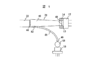
図1は、本発明の光分岐結合器及び光伝送装置の構成図である。本実施例の光伝送装置は、光分岐結合器20,光源である半導体レーザ10,光検出器12、図には示していない駆動回路,検出回路,入力端子,出力端子より構成されている。光分岐結合器20の光源接合部46に半導体レーザ10が、光検出器接合部48に光検出器12が接続されており、光ファイバ接合部44には光ファイバ22が突き合わされている。入力端子から入力された信号をもとに駆動回路により駆動された半導体レーザ10からの光信号は、光分岐結合器20を通して光ファイバ22に出力される。相手の光伝送装置から光ファイバ22を通して送られてきた光信号は、光分岐結合器20を通して光検出器12により検出され、検出回路で処理されて出力端子より出力される。
FIG. 1 is a configuration diagram of an optical branching coupler and an optical transmission apparatus according to the present invention. The optical transmission apparatus according to this embodiment includes an
このように、1本の光ファイバを用いて双方向の通信を行うことにより、送信と受信のそれぞれに光ファイバを1本ずつ用いる場合に比べて光ファイバの本数が少なくなるので低コストで光ファイバを敷設することが出来る。また、光伝送装置及び光コネクタを小型化できる。 In this way, bi-directional communication using one optical fiber reduces the number of optical fibers compared to the case of using one optical fiber for each transmission and reception. Fiber can be laid. In addition, the optical transmission device and the optical connector can be reduced in size.
本実施例の光分岐結合器20は、第一の光導波路部の検出器結合用光導波路部40と第二の光導波路部の分岐結合用光ファイバ80とからなっている。分岐結合用光ファイバ
80は、検出器結合用光導波路部40に形成された溝部82にはめ込まれており、この溝部82において分岐結合用光ファイバ80と検出器結合用光導波路部40とが接合されている。半導体レーザ10からの信号光は、ボールレンズ60により集光され分岐結合用光ファイバ80に入射する。分岐結合用光ファイバ80に入射した信号光は、光ファイバ接合部44を通り光ファイバ22に入射する。検出器結合用光導波路部40の光検出器接合部48には、光検出器12内の光検出器素子13に直接接合されている。また、検出器結合用光導波路部40には光検出器12に向かって径が小さくなるようにテーパが形成されており、光ファイバよりも径の小さな光検出器素子13に効率よく信号光を導くことができる。光検出器素子13は、大気に触れて劣化しないように、検出器結合用光導波路部
40を含めて封入用樹脂14により封入されている。
The
本実施例では、光ファイバ22にコア径1mmのPOF,分岐結合用光ファイバ80にコア径200μm,ファイバ外径230μmのハードポリマクラッドファイバ(HPCF)を用いた。したがって、光ファイバ22を通して送られてきた光信号のうち、分岐結合用光ファイバ80側に分岐して損失する光量は、約5%であり、残りの95%は検出器結合用光導波路部40側に分岐される。そのため、光分岐結合器20による分岐損失は少なく、受光光量を大きくとることが出来る。また、分岐結合用光ファイバ80の中心線は、光ファイバ接合部において光ファイバ22の中心線とほぼ平行になるように設置されている。つまり、分岐結合用光ファイバ80からの送信光は、光ファイバ接合部44の面に対してほぼ垂直に出射される。そのため、中心線が傾いている場合に比べて、光ファイバ接合部44及び光ファイバ22の端面で反射した信号光のうち検出器結合用光導波路部40に入射する光量が少なくなり、送信時のクロストークが少なくなる。さらに、光ファイバを用いているため、取り回しが容易であり、半導体レーザ10の取り付け位置を自由に定めることが出来る。
In this embodiment, a POF having a core diameter of 1 mm is used for the
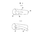
図2に本実施例の光分岐結合器20の作製手順を示す。まず、図2(a)のように、分岐結合用光ファイバ80の外形形状に合わせた溝部82を有する検出器結合用光導波路部40を透明樹脂であるポリメタクリルメタクリレート(PMMA)を用いて射出成形により形成し、コア部とした。この検出器結合用光導波路部40上に、フッ化バリウムを用い低屈折率の薄膜を蒸着し、さらにその上に金を用いて金属膜を形成した。次に、図2(b)のように、溝部82に分岐結合用光ファイバ80をはめ、端面を光ファイバ接合部44の面に合わせて接着した。
FIG. 2 shows a procedure for manufacturing the optical branching
分岐結合用光ファイバ80を用いているために、途中で検出器結合用光導波路部40側に光が漏れることがなく、クロストークが発生しない。検出器結合用光導波路部40では、低屈折率膜がクラッド層となり、検出器結合用光導波路部40に入射した信号光はコア部とクラッド層の界面で全反射し光検出器12の方に導かれる。コア部とクラッド層の界面に凹凸があり、信号光が漏れ出しても、その外側の金属層で反射し、再び検出器結合用光導波路部40に戻るため、光ファイバ22から検出器結合用光導波路部40に入射した信号光のほとんどが光検出器12で検出される。
Since the branch coupling
本実施例の分岐結合用光ファイバ80の代わりに、光導波路部を検出器結合用光導波路部40と一体で成形してもよい。
Instead of the branch coupling
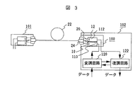
本発明の光通信装置の実施例を図3を用いて説明する。図3は光通信装置の構成図である。光伝送装置100と光伝送装置101間で双方向に通信を行う。光伝送装置100,入力信号を変調する変調回路120,光伝送装置100で検出した信号を復調し出力する復調回路122を含めて光通信装置102とする。本実施例では、光ファイバ22としてプラスチック光ファイバを用いており、光ファイバ22と光伝送装置100とは光コネクタ24により結合されている。光伝送装置101から光ファイバ22を通して光伝送装置100に送られてきた光信号は、光分岐結合器20を通して光検出器12で検出され、検出回路112に波形整形されたデジタル信号として出力される。検出回路112からの信号は、復調回路122により電気信号の形式に合わせて復調されて出力される。光通信装置102に入力された電気信号は、変調回路120により光信号として送信するのに適した符号に変換され、駆動回路110に送られる。駆動回路110により半導体レーザ10を駆動し、光分岐結合器20を通して光ファイバ22に光信号を送信する。変調回路120と復調回路122間でやり取りすることで光ファイバ22中での光信号の衝突を検出することができる。つまり、送信時は光ファイバ22の端面で反射し光検出器12で検出された信号を自分の送信信号と比較し、違いがある場合には、光伝送装置101からも信号が送られていることが分かり、衝突を検出できる。あるいは、通常の送信時に光検出器12で検出される光量よりも大きな光量が検出された場合には、衝突が起きていると判断することができる。衝突を検知した場合には、ある時間待った後再送するなど、所定の手続きで送信をやり直せばよい。
An embodiment of the optical communication apparatus of the present invention will be described with reference to FIG. FIG. 3 is a configuration diagram of the optical communication apparatus. Bidirectional communication is performed between the
このように衝突を検出するためには、光分岐結合器20のクロストークにより光検出器12で検出される光量が、システムのパワーバジェット,マージンを考慮した上で光伝送装置101から送られてくる最小光量以下となるようにすればよい。クロストークが大きく衝突が検出できない場合には、時分割通信を行うことで双方向通信を行うことができる。逆に、クロストークが少なく送信していても相手から送られてくる光データを再生できる場合には、全二重通信を行うことが出来る。
In order to detect a collision in this way, the amount of light detected by the
図4は、本発明の光分岐結合器の別の実施例の構成図である。光分岐結合器コア30は、光源結合用光導波路部38及び検出器結合用光導波路部40からなり、光分岐結合器クラッド32中に埋め込まれている。光源結合用光導波路部38の光源接合部46には半導体レーザ10,検出器結合用光導波路部40の光検出器接合部48には光検出器12が結合され、光分岐結合器クラッド32中に封入されている。本実施例においては、光源結合用光導波路部38と検出器結合用光導波路部40とを一体で射出成形した。検出器結合用光導波路部40は円錐の一部を切り出した形をしており、光検出器接合部48側から光ファイバ結合部44にかけて径が大きくなっている。光源結合用光導波路部38は円筒形をしており太さはほぼ一定である。この光結合分離素子コア30の端面を研磨し、半導体レーザ素子11及び光検出器素子13を接合し、光結合分離素子コア30,半導体レーザ素子11及び光検出器素子13を覆うように光結合分離素子クラッド32を形成した。半導体レーザ素子11及び光検出器素子13には、図示していない端子を通して電気信号の入出力を行う。
FIG. 4 is a configuration diagram of another embodiment of the optical branching coupler of the present invention. The optical
本実施例では、光源結合用光導波路部38が真っ直ぐで中心軸が光ファイバ22の中心軸とほぼ平行であることと、検出器結合用光導波路部40の一端が光ファイバ22の中心軸とほぼ平行であることに特徴がある。そのため、半導体レーザ素子11からの出射光は、光源結合用光導波路部38の中で広がらず光ファイバ22に入射する。光ファイバ22に斜めに入射した光線は、損失が大きくなり、また光信号の帯域を減少させるが、本実施例のように真っ直ぐ信号光を入射することにより、この損失の増加,帯域の低下を抑えることができる。本実施例の光分岐結合器を用いて長さ50m,開口数0.3 のステップインデックス型プラスチック光ファイバに光を送信した場合、光ファイバの帯域は、275MHzであったが、角度7°で入射する光分岐結合器を用いた場合には、200MHzに低下した。真っ直ぐ信号光を入射することにより、端面での反射によるクロストークの発生も低減できる。また、検出器結合用光導波路部40の一端を光ファイバ22の中心軸とほぼ平行とすることにより、検出器結合用光導波路部40で全反射条件を外れたことによって生じる損失を抑えることができる。またさらに、光分離結合器と半導体レーザ素子
11,光検出器素子13を一体化することにより、光伝送装置を小型化することができる。
In this embodiment, the light source coupling
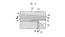
図5は、本発明の光分岐結合器のさらに別の実施例の構成図である。光源接合部46から光源結合用光導波路部38に入射した信号光は、反射面42で反射した後、光ファイバに入射する。この光分岐結合器20は、フォトリソグラフィを用いて作製した。まず、基板上にクラッド層を形成し、その上にコア層を形成した。このコア層をフォトリソグラフィにより導波路の形状を形成した。その上にまたクラッド層を形成し、再びフォトリソグラフィにより反射面42を形成した。本実施例においては、コア断面は、四角形をしている。光源結合用光導波路部38と検出器結合用光導波路部40とは高さは同じであるが、検出器結合用光導波路部40は光源側に近づくと幅が狭まっており、光源結合用光導波路部38はほぼ同じ幅を保っている。フォトリソグラフィを用いているために同時に大量に製造できる。
FIG. 5 is a block diagram of still another embodiment of the optical branching coupler of the present invention. The signal light incident on the light source coupling
本実施例では、光源と光検出器とを離して設置できるので、光源と光検出器が大きい場合、又は光分岐結合器20が小さい場合にも光源と光検出器とが互いに干渉せず設置することができる。本実施例のように、検出器結合用光導波路部40が光検出器側に向かって径が減少するようにテーパが設けられているため、光源結合用光導波路部38と検出器結合用光導波路部40の両方とも中心軸を光ファイバの中心軸と平行にすることができる。このように検出器結合用光導波路部40の中心軸を光ファイバの中心軸と平行とすることにより、検出器結合用光導波路部40内での反射による損失を最低にすることができる。
In this embodiment, since the light source and the light detector can be installed apart from each other, the light source and the light detector do not interfere with each other even when the light source and the light detector are large or when the optical branching
上記実施例以外にも、光源,光検出器と光分岐結合器の間を光ファイバを用いて結合することで、光源または光検出器の間隔を広げることができ、実装を容易にすることもできる。あるいは、光源結合用光導波路部に曲率を持たせても良い。 In addition to the above-described embodiments, the light source, the photodetector, and the optical branching coupler can be coupled using an optical fiber, so that the interval between the light sources or the photodetectors can be widened and the mounting can be facilitated. it can. Or you may give a curvature to the optical waveguide part for light source coupling | bonding.
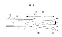
ここで、図6を用いて、光検出器接合部48のテーパ形状の寸法と光学定数との関係について説明する。上記本実施例では、テーパ形状の光導波路を用いて光を絞ることにより、コア形の大きな光ファイバを用いても面積の小さな光検出器に効率よく光を導くことのできる構造になっている。ここでは簡単のために、光ファイバ接合部44の径を光ファイバ22のコア径と同じとし、光検出器接合部48と光ファイバ22の光軸が一致している場合について説明する。光ファイバ22を伝搬してくる光線は、光ファイバ22のコア
34とクラッド36の界面で全反射を起こしながら伝搬してくるため、光ファイバ22に対してある範囲の角度をなす光線のみ光ファイバ22を通ることができる。光ファイバ
22の開口数をNAf ,光ファイバのコアの屈折率をncfとすると、光ファイバ22を伝送できる光線の光ファイバ22に対する最大の角度をψとしたとき、ψは、
Here, the relationship between the taper-shaped dimension of the photodetector joint 48 and the optical constant will be described with reference to FIG. In the present embodiment, light is focused using a tapered optical waveguide so that light can be efficiently guided to a photodetector having a small area even when a large core optical fiber is used. . Here, for the sake of simplicity, the case where the diameter of the optical fiber joint 44 is the same as the core diameter of the

と表わされる。ここで、光ファイバ及び光分岐結合器の開口数NAは、コアの屈折率を
ncore、クラッドの屈折率をncladとすると、
It is expressed as Here, the numerical aperture NA of the optical fiber and the optical branching coupler is defined as follows, where n core is the refractive index of the core and n clad is the refractive index of the cladding.
で表わされるものである。この光ファイバ22に対する最大の角度ψをなして伝搬してきた光が光検出器に到るまでテーパ形状の光検出器接合部48内で全反射して伝わる条件を示す。検出器結合用光導波路部40のテーパ部の角度をαとすると、この光線の光導波路界面への入射角度は、
π−(ψ+α)
となる。したがって、光ファイバと光導波路の開口数が等しい時には、この光線は全反射を起こさず、大部分の光が光導波路界面を透過してしまう。本発明は、光ファイバの開口数よりも光導波路の開口数の方を大きくしたことを特徴としている。光分岐結合器界面でn回目の反射時の光導波路界面への入射角度は、
π−{ψ+(2n−1)α}
となる。この光線が光導波路界面で全反射を起こすためには、コアの屈折率をncw、開口数をNAw とすると、
It is represented by Conditions under which the light propagating at the maximum angle ψ with respect to the
π- (ψ + α)
It becomes. Therefore, when the numerical apertures of the optical fiber and the optical waveguide are equal, this light beam does not cause total reflection, and most of the light is transmitted through the optical waveguide interface. The present invention is characterized in that the numerical aperture of the optical waveguide is made larger than the numerical aperture of the optical fiber. The incident angle to the optical waveguide interface at the n-th reflection at the optical coupler interface is
π− {ψ + (2n−1) α}
It becomes. In order for this ray to cause total reflection at the optical waveguide interface, if the refractive index of the core is n cw and the numerical aperture is NA w ,
を満たす必要ある。光ファイバ22に対して角度ψで伝搬してきた光の反射回数がn回以下となるためには、検出器結合用光導波路部40の長さlは、
It is necessary to satisfy. In order for the number of reflections of light propagating at an angle ψ to the
を満たす必要ある。ただし、光ファイバ接合部44の半径をRとすると、di は、 It is necessary to satisfy. However, if the radius of the optical fiber joint 44 is R, d i is
を用いて求められるものである。検出器結合用光導波路部40の長さがlのときの光検出器接合部48の半径rは、
Is required. The radius r of the photodetector joint 48 when the length of the detector coupling
(数6)
r=R−ltanα …(6)
となる。このrをなるべく小さくするように、α及びlを設定することが望ましい。式
(3)及び式(4)を満たすように光導波路の形状及び光学定数を選ぶことにより、理想的には光ファイバ22から検出器結合用光導波路部40に入射した光線はすべて検出器結合用光導波路部40界面で全反射を起こして光検出器に到るので光利用効率を大きくすることができる。このテーパ形状を用いたビーム径縮小による光検出感度の向上の効果はコア径が大きいほうが大きく、通常コア径0.5mm 以上、特に良く使われるもののコア径が約1mmであるプラスチック光ファイバと接合するときに用いるとその効果が大きい。
(Equation 6)
r = R-ltanα (6)
It becomes. It is desirable to set α and l so that r is as small as possible. By selecting the shape of the optical waveguide and the optical constant so as to satisfy the expressions (3) and (4), ideally, all the light beams incident from the
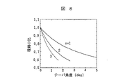
図8に式(1)から式(6)を用いて計算した光導波路部のテーパ角度αとテーパ光導波路の径の縮小率を示した。同じ縮小率を得るためには、反射回数nの大きい方がテーパ角度αを小さくできることが分かる。テーパ角度αは小さいほうが光分岐結合器を作製しやすく望ましい。図9に式(1)から式(6)を用いて計算した光分岐結合器の開口数
NAW とテーパ形状の検出器結合用光導波路部の径の縮小率を示した。計算は、NAf=0.3,NAw=0.5,ncf=ncw=1.5、とし、lが最大になる値を用いた。図より、光導波路の開口数NAw の大きい方がビーム縮小の効果が大きいことが分かる。n=2,3についてはほぼ同じ特性を示す。反射回数は少ない方が反射による損失が生じにくいため望ましい。したがって、望ましい反射回数nは、1〜3であり、n=2が特に望ましいと言える。NAf=0.3,NAw=0.5,ncw=1.5,R=0.5mm,n=2のときには、l=4.5mm、r=0.29mmとなり、ビーム径を58%に縮小することができ、そのため光のエネルギー密度は3倍に向上する。図9より、光分岐結合器の開口数を接合する光ファイバの開口数の1.5 倍以上とすると、面積比で0.4 以下にすることができ望ましい。さらに、光ファイバの開口数の2倍以上とすれば、ビーム径の縮小比0.5 以下、面積比で0.25 以下とすることができさらに望ましい。プラスチック光ファイバにおいては、高速通信用に開口数0.3 のものが用いられており、したがって、光導波路の開口数は、0.45 以上、できれば0.6 以上が望ましい。通常光通信に用いられている波長は570nmから1550nm程度であり、この範囲内の使用する波長においてこの開口数以上であればよい。
FIG. 8 shows the taper angle α of the optical waveguide portion and the reduction ratio of the diameter of the tapered optical waveguide calculated using the equations (1) to (6). It can be seen that in order to obtain the same reduction ratio, the taper angle α can be reduced as the number of reflections n increases. A smaller taper angle α is desirable because an optical branch coupler can be easily manufactured. FIG. 9 shows the numerical aperture NA W of the optical branching coupler calculated using the equations (1) to (6) and the reduction ratio of the diameter of the tapered detector coupling optical waveguide portion. In the calculation, NA f = 0.3, NA w = 0.5, n cf = n cw = 1.5, and a value that maximizes l was used. From the figure, it is seen that a large numerical aperture NA w of the optical waveguide is large, the effect of beam reduction. About n = 2 and 3, the same characteristic is shown. A smaller number of reflections is desirable because loss due to reflection is less likely to occur. Therefore, the desirable number of reflections n is 1 to 3, and it can be said that n = 2 is particularly desirable. When NA f = 0.3, NA w = 0.5, n cw = 1.5, R = 0.5 mm, and n = 2, l = 4.5 mm and r = 0.29 mm, and the beam diameter is 58 %, So that the energy density of light is improved three times. From FIG. 9, when the numerical aperture of the optical branching coupler is 1.5 times or more the numerical aperture of the optical fiber to be joined, the area ratio is preferably 0.4 or less. Furthermore, if the numerical aperture of the optical fiber is set to be twice or more, it is more preferable that the reduction ratio of the beam diameter is 0.5 or less and the area ratio is 0.25 or less. A plastic optical fiber having a numerical aperture of 0.3 is used for high-speed communication. Therefore, the numerical aperture of the optical waveguide is preferably 0.45 or more, preferably 0.6 or more. The wavelength normally used for optical communication is about 570 nm to 1550 nm, and it is sufficient that the wavelength used is within this range as long as the numerical aperture.
以上のように、開口数、つまりコア部とクラッド部の屈折率差が大きい方が光閉じ込めの効果が大きくなり望ましい。開口数を大きくするために、コア部とクラッド部の界面に低屈折率の誘電体膜を形成してもよい。さらに誘電体膜とクラッド部の界面にさらに金属膜を形成すると、開口数を超え、誘電体膜を透過したビームも金属膜で反射し戻るので、上記条件以上にビーム径を縮小することが可能となる。 As described above, it is desirable that the numerical aperture, that is, the refractive index difference between the core portion and the clad portion is large, because the effect of optical confinement becomes large. In order to increase the numerical aperture, a low refractive index dielectric film may be formed at the interface between the core portion and the cladding portion. Furthermore, if a metal film is further formed at the interface between the dielectric film and the clad, the beam diameter that exceeds the numerical aperture and the beam that has passed through the dielectric film is reflected back by the metal film. It becomes.
光分岐結合器の実施例として、コア材としてポリスチレン(屈折率1.59)、クラッド材としてポリメチルペンテン系(屈折率1.46)を用いた。このとき、波長650nmにおいて開口数0.63 となる。したがって、図9より求められるようにn=2を用いて、径縮小比0.4、面積比で0.16となった。 As an example of the optical branching coupler, polystyrene (refractive index 1.59) was used as the core material, and polymethylpentene (refractive index 1.46) was used as the cladding material. At this time, the numerical aperture is 0.63 at a wavelength of 650 nm. Therefore, as obtained from FIG. 9, using n = 2, the diameter reduction ratio becomes 0.4 and the area ratio becomes 0.16.
以上、光検出器接合部48と光ファイバ22の光軸が一致している場合について説明したが、光検出器接合部48が光ファイバ22に対して傾けて設けることも出来る。光検出器接合部48を傾けることにより損失が発生するが、光検出器接合部48の1辺が光ファイバ22の光軸と平行になる角度以下では、光検出器接合部48と光ファイバ22の光軸が一致している場合から顕著な損失の増加は起こらないため、望ましい。また、テーパ角度を緩くすることにより損失が発生しないようにすることもできる。
The case where the optical axes of the photodetector joint 48 and the
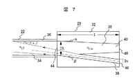
次に、図7を用いて光源結合用光導波路部38の傾きについて、光源結合用光導波路部38から光ファイバに入射した光線がすべて光ファイバの界面で全反射する条件を示す。光源からの広がり角Θの光線が光ファイバに入射したときの光線の広がり角θは、
Next, with reference to FIG. 7, the inclination of the light source coupling
となる。光源結合用光導波路部38の傾きをβとすると、この光線が光ファイバの界面で全反射するためには、
It becomes. If the inclination of the light source coupling
を満たす必要がある。βを大きくすると光源と光検出器の間隔を広く取ることができるので光源と光検出器の実装が容易になる。その際には、式(8)よりθを小さくする必要がある。半導体レーザは、発光ダイオードに比べて広がり角θが小さい。特に本発明の光伝送装置に用いる光源として好適な光源の一例は、面発光型半導体レーザである。通常、面発光半導体レーザの広がり角は、1/e2半角で5°程度であり、NAs としては0.09程度である。NAf=0.3,NAs=0.1,ncf=1.5とすると、βを7.7°以下とすればよく、光源結合用光導波路部38の半径をsとすると、NAw=0.5 ,ncw=1.5,R=0.5mm,r=0.29mm,s=0.125mm,l=4.3mm,n=2のとき、光源接合部46と光検出器接合部48との間隔は0.5mmとなる。高速通信用の開口数0.3のプラスチック光ファイバに対しては、sinΘを0.1以下とすれば、光源結合用光導波路部
38と検出器結合用光導波路部40との間隔を広くでき望ましい。端面発光型の半導体レーザや発光ダイオードを光源に用いた場合のように、光源の広がり角が大きい場合には、光源と光源結合用光導波路部38のあいだに広がり角を制限するためのピンホールを設けてもよい。またあるいは、光源結合用光導波路部38を光源接合部46から光ファイバ接合部44にかけて断面積が増加するようにテーパ形状としてもよい。光源からの光線に強度分布がある場合には、強度分布の1/e2 半角を式(10)のΘとして用いればよい。
It is necessary to satisfy. If β is increased, the distance between the light source and the photodetector can be increased, so that the mounting of the light source and the photodetector becomes easy. In that case, it is necessary to make θ smaller than the equation (8). A semiconductor laser has a smaller divergence angle θ than a light emitting diode. One example of a light source that is particularly suitable as a light source for use in the optical transmission device of the present invention is a surface emitting semiconductor laser. Usually, the spread angle of a surface emitting semiconductor laser is about 5 ° in 1 / e 2 half angle, and NA s is about 0.09. If NA f = 0.3, NA s = 0.1, n cf = 1.5, β may be 7.7 ° or less, and if the radius of the light source coupling
このように、光源結合用光導波路38を光ファイバに対して斜めに配しても、効率よく光ファイバに信号光を入射することができる。しかし、光ファイバに斜めに光を入射する場合、光ファイバ内での伝送損失が増加し、伝送帯域も減少するため、光源結合用光導波路部38と光ファイバとの傾きは小さいことが望ましく、ほぼ平行となる配置がもっとも望ましい。
Thus, even if the light source coupling
光源結合用光導波路部38の径を光ファイバ接合部44の径よりも小さくすることで、光ファイバ22から光分岐結合器20に入射する光量のうち、検出器結合用光導波路部
40に分岐される光量の割合を大きくすることができる。分岐比は各光導波路部の面積にほぼ比例するため、例えば、光源結合用光導波路部38の径を光ファイバ接合部44の径の1/4とすると、光源結合用光導波路部38と検出器結合用光導波路部40に分岐される光量の割合の割合は、ほぼ1:9となる。このように、光源結合用光導波路部38の径を光ファイバ接合部44の径の1/4以下とすることで光損失は、10%以下となり望ましい。光源結合用光導波路部38の径を光ファイバ接合部44の径の1/10以下とすることで光損失は、1%以下となりさらに望ましい。したがって、コア半径0.5mm のプラスチック光ファイバを用いた場合には、光ファイバ接合部44の半径0.5mm に対し、光源結合用光導波路部38の半径を0.125mm以下、出来れば0.05mm以下とすることが望ましい。
By making the diameter of the light source coupling
本発明の光分岐結合器のコア及びクラッドの材料には、所望の開口数となるように、アクリル系,メタクリル系,カルボネート系,非晶質オレフィン系,スルホン系,シリコーン系,ビニル系,フッ素系化合物等を適宜組み合わせて用いることができる。本発明の光分岐結合器はその形状に特徴があるので、材料は有機材料に限るものではなく、ガラス,酸化シリコン,窒化シリコン等の透明無機材料,薄膜材料を用いてもよい。また、作製方法も、射出整形法,紫外線硬化法,ウェットエッチング法,反応性イオンエッチング法,光重合法等の光導波路を作製する方法、あるいは、光ファイバを接合する方法等適宜選択して光分岐結合器を作製すればよい。 The core and clad materials of the optical branch coupler of the present invention are acrylic, methacrylic, carbonate, amorphous olefin, sulfone, silicone, vinyl, fluorine, so as to have a desired numerical aperture. These compounds can be used in appropriate combination. Since the optical branching coupler of the present invention is characterized by its shape, the material is not limited to an organic material, and a transparent inorganic material such as glass, silicon oxide, or silicon nitride, or a thin film material may be used. In addition, the manufacturing method is appropriately selected, such as a method of manufacturing an optical waveguide such as an injection shaping method, an ultraviolet curing method, a wet etching method, a reactive ion etching method, a photopolymerization method, or a method of joining optical fibers. A branch coupler may be manufactured.
本発明の光分岐結合器の断面形状は、接合する光ファイバと同じくする必要はなく、例えば四角形の断面形状を用いてもよい。四角形の断面形状の場合には、光ファイバ接合部の一辺の長さを光ファイバ直径よりも大きくし、光源結合用光導波路部38を光源結合用光導波路部38から出射される光線がすべて円形の光ファイバに入射するように光源接合部からずらして接合するればよい。このようにずらすことにより四角形の断面形状を用いても円形の断面形状をした光ファイバに効率よく光を結合することができる。
The cross-sectional shape of the optical branching coupler of the present invention is not necessarily the same as the optical fiber to be joined, and for example, a quadrangular cross-sectional shape may be used. In the case of a square cross-sectional shape, the length of one side of the optical fiber joint is made larger than the diameter of the optical fiber, and the light source coupling
これまで、2つに分岐した光分岐結合器について説明してきたが、本発明は分岐を2つに限るものではなく、2つ以上に分岐する場合にも適用できる。 So far, the optical branching coupler branched into two has been described, but the present invention is not limited to two, but can be applied to the case where two or more branches are branched.
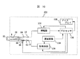
図10は、本発明の光パルス試験機の実施例の構成図である。本実施例の光パルス試験機150は、光時間領域反射測定法(Optical Time Domain Reflectivity:OTDR)を用いたものである。半導体レーザ10は、駆動回路130によりパルス駆動され、パルス光を出射する。このパルス光は、ボールレンズ60で集光されて光ファイバ84を通り、光減衰器66で光量を調整して光分岐結合器20に入射する。光分岐結合器20から被測定用の光ファイバ22に入射する。光ファイバ22内で散乱,反射されて戻ってきた検出光は、光分岐結合器20から光ファイバ86に導かれ、光検出器12で検出される。光検出器12で検出された信号は、増幅器132で増幅され、プロセッサ136に取り込まれる。プロセッサ136で処理された信号はディスプレイに表示される。プロセッサでは、図示していないパネルからの入力をもとに、信号の積算,スムージング,ピーク検出,損失測定,時間の距離変換,レイリー散乱・フレネル反射測定の切り替え、等の処理を行う。駆動回路130の光パルスの発生開始・終了、光パルス幅は、プロセッサ136により制御されている。光パルスの発生に同期して駆動回路130から出力されるトリガー信号は、遅延回路134により一定時間遅延されて、プロセッサ136に入力される。プロセッサ136は、遅延回路134からトリガー信号をもとに増幅器132からの信号の取り込みを開始する。また、増幅器132からの信号が所定の水準となるように、光減衰器
66の透過率と増幅器132のゲインを制御する。
FIG. 10 is a configuration diagram of an embodiment of the optical pulse testing machine of the present invention. The
本実施例では、半導体レーザ10に波長650nmのものを用い、光検出器12にシリコンアバランシェホトダイオードを用いた。アバランシェホトダイオードへの印加電圧を制御することにより信号のゲインを調整することもできる。
In this embodiment, the
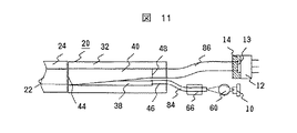
図11に、本実施例に用いた光分岐結合器及び光学系の実施例を示す。光分岐結合器
20には、既に図4で説明したものを用いた。半導体レーザ10からのパルス光は、ボールレンズ60で集光されてコア径100μmのハードポリマクラッドファイバ(HPCF)を用いて光ファイバ84に入射する。光パルスは、光ファイバ84の途中に設けられた光減衰器66で光量を調整され、光分岐結合器20の光源接合部46より光源結合用光導波路部38に入射し、光ファイバ22に結合される。光ファイバ22は、所定の位置にくるように、光コネクタ24を用いて光パルス試験機150に繋がれている。光ファイバ22内で散乱,反射されて戻ってきた検出光は、光分岐結合器20の検出器結合用光導波路部40で集光され、光ファイバ86に導かれる。光ファイバ86のもう一端には、光検出器素子13が結合されており、光検出器素子13は、大気に触れて劣化しないように、光ファイバ86を含めて封入用樹脂により封入されている。光ファイバ84,86は、光分岐結合器20に結合され固定されている。本実施例では、光ファイバ84にコア径0.5mm,開口数0.6のPOFを用いた。また、光ファイバ接合端は、直径1.1mmとした。そのため、コア径1.1mm 以下の光ファイバについて効率良くOTDR測定が出きる。本実施例においては、径の小さな光ファイバにも効率よくパルス光を入射できるように、光分岐結合器20の位置を移動できるようにした。検出光量が最大となるように光ファイバ22に対して光分岐結合器20を移動する。つまり、径の細い光ファイバについては、光分岐結合器20を図の上方に移動すればよい。このように移動することにより、本実施例では、コア径150μmの光ファイバにおいても、光ファイバからの検出光のうち半分以上を光検出器に結合することができる。つまり、光源結合用光導波路部38の径に対し、コア径が1.5 倍以上の光ファイバについて、効率良く測定できるようになる。
FIG. 11 shows an embodiment of the optical branching coupler and optical system used in this embodiment. As the optical branching
本実施例では、光分岐結合器20と半導体レーザ10,光検出器12とを光ファイバ用いて繋いでるため、取り回しが容易であり、取り付け位置を自由に定めることが出来る。そのため、光源,光検出器を自由に選ぶことができ、高出力な光源や感度の高い光検出器12を用いることも出来る。また本実施例のように、光分岐結合器20を移動することができる。本発明の光パルス試験機に用いる光分岐結合器20は、本実施例に限るものではなく、本発明のすべての光分岐結合器を用いることが出来る。
In this embodiment, since the optical branching
光源結合用光導波路部38に傾きを持たせ、光源結合用光導波路部38からの出射光が光ファイバ接合部44の中心を通るように光源結合用光導波路部38の取り付け位置をずらした光分岐結合器20を用いる場合には、光分岐結合器20を固定しておいても、径の細い光ファイバのOTDR測定が可能である。
Light in which the mounting position of the light source coupling
以上、光分岐結合器の光ファイバ接合部と光ファイバとを直接突き合わせている実施例を用いて本発明の光分岐結合器を説明してきたが、光ファイバ接合部に光ファイバを接合し、この光ファイバと通信用または被測定用のファイバを光コネクタを用いて接続してもよい。 As described above, the optical branch coupler of the present invention has been described using the embodiment in which the optical fiber joint of the optical branch coupler and the optical fiber are directly abutted, but the optical fiber is joined to the optical fiber joint, An optical fiber and a fiber for communication or measurement may be connected using an optical connector.
本発明の光パルス試験機は、検出光の分離の難しいコア径の大きな光ファイバに適したものであり、したがって、コア径の大きなプラスチック光ファイバに用いると効果がある。通常用いられるプラスチック光ファイバのコア径は、0.5mm 以上,2mm以下程度であるので、光パルス試験機の光コネクタにおいて光パルス試験機側の接続部の径を特に0.5
mm以上,2mm以下とすることが望ましい。
The optical pulse tester according to the present invention is suitable for an optical fiber having a large core diameter in which detection light is difficult to be separated, and is therefore effective when used for a plastic optical fiber having a large core diameter. Since the core diameter of plastic optical fiber that is usually used is about 0.5 mm or more and 2 mm or less, the diameter of the connection part on the optical pulse testing machine side is particularly 0.5.
It is desirable to set it to mm or more and 2 mm or less.
ここで、OTDRの位置分解能と、被測定用光ファイバの帯域と長さの関係について示す。光ファイバコアの屈折率nが既知であれば入射光が散乱して戻ってくるまでの時間tからその散乱位置zを Here, the relationship between the OTDR position resolution and the bandwidth and length of the optical fiber to be measured will be described. If the refractive index n of the optical fiber core is known, the scattering position z is determined from the time t until the incident light is scattered and returned.
(数9)
z=ct/2n …(9)
より求めることができる。このとき、位置分解能Δzは、光ファイバ伝送前のパルス幅をW、単位長さにおける伝送帯域をF、伝送距離をLとすると、
(Equation 9)
z = ct / 2n (9)
It can be obtained more. At this time, if the position resolution Δz is W as the pulse width before the optical fiber transmission, F as the transmission band in the unit length, and L as the transmission distance,
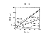
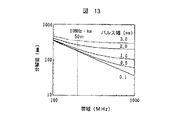
と表される。POFといった伝送損失が大きく短距離で用いられる光ファイバのOTDR測定は、高分解能であることが望まれる。図12にファイバ長と分解能の関係を示す。ファイバの帯域については10,20,100MHz・km、パルス幅について0,0.1,0.5,1.0ns の場合を示している。帯域の狭い場合には、短パルスを用いても光ファイバの帯域により分解能が劣化し、10MHz・kmにおいては、50m以上伝送するとパルス幅0.1nsと0.5nsでほとんど差がなくなることが分かる。逆に100MHz・kmで分解能を劣化させないためには、0.1ns 程度のパルス幅が必要であることが分かる。図13にファイバの帯域と分解能の関係について、パルス幅0.1から3.0nsの場合について示した。たとえば、開口数0.3 のステップインデックスプラスチック光ファイバに当たる10MHz・kmの帯域において、長さ50mに相当するのは200MHzであり、この帯域においては、入射パルス幅0であっても分解能175mmとなる。図よりパルス幅1nsであれば、分解能は余り劣化せず、202mmを得られることが分かる。分解能を光ファイバによって必然的に決まる分解能に対してα倍以下の劣化に抑えるにためは、入射するパルス幅Wは、 It is expressed. OTDR measurement of an optical fiber having a large transmission loss such as POF and used in a short distance is desired to have high resolution. FIG. 12 shows the relationship between the fiber length and the resolution. The case of the fiber band is 10, 20, 100 MHz · km, and the pulse width is 0, 0.1, 0.5, 1.0 ns. When the bandwidth is narrow, the resolution is degraded by the bandwidth of the optical fiber even when a short pulse is used, and at 10 MHz / km, when transmitting 50 m or more, there is almost no difference between the pulse width of 0.1 ns and 0.5 ns. . Conversely, it can be seen that a pulse width of about 0.1 ns is necessary in order not to degrade the resolution at 100 MHz · km. FIG. 13 shows the relationship between the bandwidth of the fiber and the resolution when the pulse width is 0.1 to 3.0 ns. For example, in a band of 10 MHz · km corresponding to a step index plastic optical fiber having a numerical aperture of 0.3, the length corresponding to 50 m is 200 MHz, and in this band, the resolution is 175 mm even when the incident pulse width is zero. . From the figure, it can be seen that if the pulse width is 1 ns, the resolution is not deteriorated so much and 202 mm can be obtained. In order to suppress the resolution to α times or less of the resolution inevitably determined by the optical fiber, the incident pulse width W is
を満たす必要がある。したがって、光ファイバの帯域F,長さLが予め分かっている場合には、
を満たす最大のパルス幅Wを選択すれば、分解能の劣化は50%以下に留めたままで、測定のダイナミックレンジを最大にすることができる。フレネル反射モードで、光ファイバの出射端から反射されて戻ってくるパルスの遅延時間及びパルス幅を測定することにより、光ファイバの帯域F,長さLを測定することができる。この光ファイバの帯域F,長さLを用いて、光パルス試験機が自動的に最適なパルス幅を選択することができる。 If the maximum pulse width W that satisfies the above is selected, the degradation of resolution remains at 50% or less, and the measurement dynamic range can be maximized. By measuring the delay time and pulse width of the pulse reflected and returned from the output end of the optical fiber in the Fresnel reflection mode, the band F and length L of the optical fiber can be measured. Using the band F and length L of the optical fiber, the optical pulse tester can automatically select the optimum pulse width.
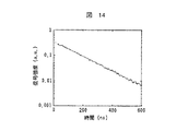
図14は、本実施例の光パルス試験機を用いてNA0.3 ,コア径1mm,長さ100mのステップインデックス(SI)型POFを測定した結果を示す。用いた半導体レーザからは、パルス幅70ps,パワー160mW,最大繰り返し周波数1MHzであり、波長は、654nmであった。この条件において、POF長25mでの分解能は、9.5cm 以下の分解能が得られる。積算を10,000 回行った結果、長さ50m以上の測定が可能であった。
FIG. 14 shows the results of measuring a step index (SI) type POF with NA 0.3,
本実施例のように、本発明の光分離結合器を用いることにより、PBSを用いた従来の光パルス試験機よりも、光検出器に結合できる検出光量を大きくすることができ、測定のダイナミックレンジを広くすることができる。したがって、半導体レーザを光源に用い、ホトダイオードあるいはアバランシェホトダイオードを光検出器に用いても、実用的な長さのプラスチック光ファイバのOTDR測定を行うことができるようになった。 As in this embodiment, by using the optical separator / coupler of the present invention, the amount of light that can be coupled to the photodetector can be made larger than that of the conventional optical pulse tester using PBS, and the measurement dynamics can be increased. The range can be widened. Therefore, even if a semiconductor laser is used as a light source and a photodiode or an avalanche photodiode is used as a photodetector, OTDR measurement of a plastic optical fiber having a practical length can be performed.
光検出器にフォトンカウンタを用いれば、さらにダイナミックレンジを広くすることが出来、さらに長い距離の測定が可能となる。また、積算回数をさらに多くとることによってもダイナミックレンジを広くすることができる。 If a photon counter is used for the photodetector, the dynamic range can be further widened, and a longer distance can be measured. The dynamic range can also be widened by increasing the number of integrations.
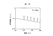
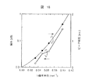
図15に光ファイバに半径15mmのループを5個形成した場合のOTDR信号を示す。ループを作った位置に対応して、OTDR信号のピークが観測された。図16に曲率半径の逆数とピークの高さ及びループによる損失を示した。損失は、ループ1個当たりのものある。ピーク強度,損失の対数とも1/Rに比例して変化している。ステップインデックス光ファイバでは、このようにOTDR信号のピークの高さを測定することにより、光ファイバの曲がりの曲率に変換することができる。本実施例の光パルス試験機では、ピークの高さを測定し、その大きさから曲がりの曲率に換算する機能を有している。 FIG. 15 shows an OTDR signal when five loops having a radius of 15 mm are formed in the optical fiber. Corresponding to the position where the loop was formed, the peak of the OTDR signal was observed. FIG. 16 shows the reciprocal of the radius of curvature, the peak height, and the loss due to the loop. The loss is per loop. Both the peak intensity and the logarithm of loss change in proportion to 1 / R. The step index optical fiber can be converted into the curvature of the optical fiber by measuring the peak height of the OTDR signal in this way. The optical pulse testing machine of the present embodiment has a function of measuring the height of the peak and converting it from the size into the curvature of bending.
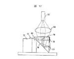
図17は、本発明の光パルス試験機に用いた光学系の実施例の構成図である。マウント72に据え付けられた半導体レーザ素子11からのビームは、レンズ62によりその広がり角を小さくされ、偏光ビームスプリッタ(PBS)に入射する。本実施例では、薄型のPBSを用いており、PBSの接合面全体にPBS膜70を形成すればよいので、プリズムの一部にPBS膜を形成するよりも作製が容易である。PBS膜70で反射したパルス光はレンズ64の中心部で集光され光ファイバ22に入射する。PBS膜70で反射しなかったビームは吸収部材76で吸収される。光ファイバ22からの検出光は、入射パルス光の広がり角よも広いため、レンズ64の広い面積を通り、全反射ミラ78で反射して、光検出器素子13で検出される。検出光のうちPBS膜70を通ったものは、その内約半分の光量がPBS膜70で反射し損失となる。しかし、その面積は検出光の占める面積に対して少ないため、PBS膜70での損失は、全検出光量に対して少ない。図には示していないが、光学系全体を気密封入した。
FIG. 17 is a configuration diagram of an embodiment of an optical system used in the optical pulse tester of the present invention. The beam from the
レンズ62を用いることにより、検出光の中でPBS膜70で損失する面積を小さくすることができ、PBS膜70での損失を少なくすることが出来る。また、それぞれのビームは光学部品の面に対して垂直に入射するため、収差が増加することなく、光検出器に光を結合するのが容易である。本実施例は、光ファイバの開口数が大きいほうが、PBS膜70で損失する検出光量が少なくなり、望ましい。
By using the
10…半導体レーザ、11…半導体レーザ素子、12…光検出器、13…光検出器素子、14…封入用樹脂、20…光分岐結合器、22…ファイバ、24…光コネクタ、30…分岐結合器コア、32…分岐結合器クラッド、34…光ファイバコア、36…光ファイバクラッド、38…光源結合用光導波路部、40…検出器結合用光導波路部、42…反射面、44…光ファイバ接合部、46…光源接合部、48…検出器接合部、60…ボールレンズ、62,64…レンズ、66…光減衰器、68…プリズム、70…PBS膜、72…マウント、74…基板、76…吸収部材、78…全反射ミラ、80…分岐結合用光ファイバ、82…溝部、84,86…光ファイバ、100…光送装置、102…光通信装置、110…駆動回路、112…検出回路、114…入力端子、116…出力端子、120…変調回路、122…復調回路、130…駆動回路、132…増幅器、134…遅延回路、136…プロセッサ、138…ディスプレイ、140…光減衰器、150…光パルス試験機。
DESCRIPTION OF
Claims (9)
前記第一の光導波路の断面積が、前記接合部から分岐方向に向けて減少するテーパ形状をなしており、
前記第二の光導波路は、前記接合部の端面に対して概ね垂直に設けられた光分岐結合器。 In the optical branching coupler having the optical waveguide portion branched into at least the first optical waveguide and the second optical waveguide from the joint portion,
The cross-sectional area of the first optical waveguide has a tapered shape that decreases in the branch direction from the joint,
The second optical waveguide is an optical branching coupler provided substantially perpendicular to the end face of the joint.
前記第二の光導波路が光ファイバであり、前記第一の光導波路に有した溝部に前記第二の光導波路が接合された光分岐結合器。 In the optical branching and coupling part of claim 1,
An optical branching coupler in which the second optical waveguide is an optical fiber, and the second optical waveguide is joined to a groove provided in the first optical waveguide.
前記接合部において、前記第二の光導波路の断面積が、前記第一の光導波路の断面積よりも小さい光分岐結合器。 The optical branching coupler according to claim 1,
An optical branching coupler in which the cross-sectional area of the second optical waveguide is smaller than the cross-sectional area of the first optical waveguide at the junction.
光ファイバからの光線を検出する光検出器と、
前記光ファイバと前記光源及び前記光検出器をそれぞれ接合する少なくとも第一の光導波路と第二の光導波路の二つに分岐された1つの光導波路部を有する光分岐結合器を有し、
前記第一の光導波路は、前記光検出器と接合され、前記第一の光導波路の断面積は、前記光ファイバから前記光検出器方向に向けて減少するテーパ形状である光伝送装置。 A light source;
A photodetector for detecting light from the optical fiber;
An optical branching coupler having one optical waveguide portion branched into at least a first optical waveguide and a second optical waveguide for joining the optical fiber, the light source, and the photodetector, respectively;
The first optical waveguide is joined to the photodetector, and the cross-sectional area of the first optical waveguide is a tapered shape that decreases from the optical fiber toward the photodetector.
前記第二の光導波路は、前記光源と接合され、前記第一の光導波路との接合部端面に対して概ね垂直に設けられた光伝送装置。 The optical transmission device according to claim 4.
The second optical waveguide is bonded to the light source, and is provided in an approximately vertical direction with respect to a joint end surface with the first optical waveguide.
前記光検出器は、前記第一の光導波路の端面部に接合されている光検出素子を有する光伝送装置。 The optical transmission device according to claim 4 or 5,
The optical detector is an optical transmission device having a photodetecting element bonded to an end surface portion of the first optical waveguide.
光源と、光検出器と、前記変調部にて変調された信号を送信するために前記光源を駆動する駆動部と、前記光源から光信号を外部へ導き、外部からの光信号を前記光検出器へ導く、少なくとも第一の光導波路及び第二の光導波路の2つの光導波路を接合させた光導波路部と、前記光検出器を駆動する検出駆動部とを有する光伝送部と、
前記光検出器で検出された信号を電気信号に復調させる復調部とを有し、
前記第一の光導波路の断面積が、外部から送信される信号の入力側から前記光検出器の方向に向けて減少するテーパ形状をなしており、前記第二の光導波路は、前記第一の光導波路との接合部端面に対して概ね垂直に設けられた光通信装置。 A modulator that converts an input signal to be transmitted into a signal for transmission;
A light source, a light detector, a drive unit for driving the light source to transmit a signal modulated by the modulation unit, a light signal from the light source to the outside, and a light signal from the outside to the light detection An optical transmission unit having an optical waveguide unit that joins at least two optical waveguides, i.e., the first optical waveguide and the second optical waveguide, and a detection driving unit that drives the photodetector;
A demodulator that demodulates the signal detected by the photodetector into an electrical signal;
The cross-sectional area of the first optical waveguide has a tapered shape that decreases from the input side of a signal transmitted from the outside toward the photodetector, and the second optical waveguide is the first optical waveguide. An optical communication device provided substantially perpendicular to the end face of the joint with the optical waveguide.
光検出器と、
前記光源からの光線を被測定体に導き、前記被測定体からの光線を前記光検出器に導く光分岐結合部と、
前記光検出部で検出された検出信号を増幅する増幅部と、
前記増幅部にて増幅された信号を処理する情報処理部と、
前記情報処理部からの指示により前記光源を駆動する駆動部とを有し、
前記光分岐結合部は、少なくとも第一の光導波路と第二の光導波路が接合されて形成され、前記第一の光導波路の断面積が、外部から送信される信号の入力側から前記光検出器の方向に向けて減少するテーパ形状をなしており、前記第二の光導波路は、前記第一の光導波路との接合端面に対して概ね垂直に設けられた光パルス試験機。 A light source;
A photodetector;
A light branching and coupling unit that guides a light beam from the light source to a measurement object, and guides a light beam from the measurement object to the photodetector;
An amplifying unit for amplifying a detection signal detected by the photodetecting unit;
An information processing unit for processing the signal amplified by the amplification unit;
A drive unit that drives the light source according to an instruction from the information processing unit,
The optical branching and coupling part is formed by joining at least a first optical waveguide and a second optical waveguide, and the cross-sectional area of the first optical waveguide is detected from the input side of a signal transmitted from the outside. An optical pulse tester having a taper shape that decreases in the direction of the vessel, and wherein the second optical waveguide is provided substantially perpendicular to a joint end surface with the first optical waveguide.
前記被測定体と前記光分岐結合部の接合部の径が0.5mm 以上2mm以下である光パルス試験機。
The optical pulse tester according to claim 8,
An optical pulse tester in which a diameter of a joint portion between the measured object and the optical branching coupling portion is 0.5 mm or more and 2 mm or less.
Priority Applications (1)
| Application Number | Priority Date | Filing Date | Title |
|---|---|---|---|
| JP2005115228A JP2005292843A (en) | 2005-04-13 | 2005-04-13 | Optical transmission device and optical pulse tester |
Applications Claiming Priority (1)
| Application Number | Priority Date | Filing Date | Title |
|---|---|---|---|
| JP2005115228A JP2005292843A (en) | 2005-04-13 | 2005-04-13 | Optical transmission device and optical pulse tester |
Related Parent Applications (1)
| Application Number | Title | Priority Date | Filing Date |
|---|---|---|---|
| JP06115899A Division JP3726536B2 (en) | 1999-03-09 | 1999-03-09 | Optical transmission device and optical pulse tester |
Publications (2)
| Publication Number | Publication Date |
|---|---|
| JP2005292843A true JP2005292843A (en) | 2005-10-20 |
| JP2005292843A5 JP2005292843A5 (en) | 2006-02-02 |
Family
ID=35325756
Family Applications (1)
| Application Number | Title | Priority Date | Filing Date |
|---|---|---|---|
| JP2005115228A Withdrawn JP2005292843A (en) | 2005-04-13 | 2005-04-13 | Optical transmission device and optical pulse tester |
Country Status (1)
| Country | Link |
|---|---|
| JP (1) | JP2005292843A (en) |
Cited By (2)
| Publication number | Priority date | Publication date | Assignee | Title |
|---|---|---|---|---|
| KR101227039B1 (en) * | 2012-09-10 | 2013-01-28 | 주식회사 피피아이 | Optical power monitoring module |
| CN115560729A (en) * | 2022-08-04 | 2023-01-03 | 西安航天精密机电研究所 | A Method for Measuring and Compensating the Slope of Y-Waveguide Waveform |
-
2005
- 2005-04-13 JP JP2005115228A patent/JP2005292843A/en not_active Withdrawn
Cited By (3)
| Publication number | Priority date | Publication date | Assignee | Title |
|---|---|---|---|---|
| KR101227039B1 (en) * | 2012-09-10 | 2013-01-28 | 주식회사 피피아이 | Optical power monitoring module |
| CN115560729A (en) * | 2022-08-04 | 2023-01-03 | 西安航天精密机电研究所 | A Method for Measuring and Compensating the Slope of Y-Waveguide Waveform |
| CN115560729B (en) * | 2022-08-04 | 2025-12-16 | 西安航天精密机电研究所 | Y-waveguide waveform inclination measurement and compensation method |
Similar Documents
| Publication | Publication Date | Title |
|---|---|---|
| CN112740062B (en) | Optical sensor chip | |
| US7654750B2 (en) | Bidirectional optical fiber link systems component couplers | |
| CN103874945B (en) | The equipment for receiving the optical sensor of optical signal from waveguide with multiple | |
| KR101744281B1 (en) | photonic integrated circuit comprising light turning micro mirror interior of optical waveguide and method of manufacturing thereof | |
| CA2298870A1 (en) | Light transmitting/receiving module | |
| CN101464545A (en) | Method and apparatus for monitoring light | |
| CN107532967A (en) | Wafer-level testing of optical devices | |
| US20080089644A1 (en) | Optical fiber for out-coupling optical signal and apparatus for detecting optical signal using the same optical fiber | |
| TWI628483B (en) | Optical block with textured surface | |
| TWI717047B (en) | Test device and heterogeneously integrated structure | |
| US7773640B2 (en) | Fiber laser device | |
| US8873893B2 (en) | Nano-wire optical block devices for amplifying, modulating, and detecting optical signals | |
| GB2332318A (en) | Low power output monitoring tap | |
| US20140217270A1 (en) | Light-receiving module | |
| JP2005292843A (en) | Optical transmission device and optical pulse tester | |
| JP3726536B2 (en) | Optical transmission device and optical pulse tester | |
| TW200540482A (en) | Optical power monitoring apparatus, optical power monitoring method, and light receiving device | |
| JP2004240415A (en) | Optical fiber tap | |
| US6778585B2 (en) | VCSEL monitoring using refracted ray coupling | |
| FR2688319A1 (en) | HIGH INSULATION OPTICAL COUPLER. | |
| CN115407450A (en) | Optical waveguide and method for beam assisted alignment | |
| JP2011150287A (en) | Optical transmitting and receiving device using one pof, and optical transmitting and receiving system | |
| JP4555269B2 (en) | Fiber type coupler, light detection device, and laser module | |
| KR101023136B1 (en) | Optical module device with optical fiber network monitoring device | |
| JP2007258399A (en) | Photo coupler |
Legal Events
| Date | Code | Title | Description |
|---|---|---|---|
| A521 | Written amendment |
Free format text: JAPANESE INTERMEDIATE CODE: A523 Effective date: 20051209 |
|
| A621 | Written request for application examination |
Free format text: JAPANESE INTERMEDIATE CODE: A621 Effective date: 20051209 |
|
| RD01 | Notification of change of attorney |
Free format text: JAPANESE INTERMEDIATE CODE: A7421 Effective date: 20060421 |
|
| A761 | Written withdrawal of application |
Free format text: JAPANESE INTERMEDIATE CODE: A761 Effective date: 20070126 |