JP2005292833A - Liquid crystal display device and manufacturing method thereof - Google Patents
Liquid crystal display device and manufacturing method thereof Download PDFInfo
- Publication number
- JP2005292833A JP2005292833A JP2005102405A JP2005102405A JP2005292833A JP 2005292833 A JP2005292833 A JP 2005292833A JP 2005102405 A JP2005102405 A JP 2005102405A JP 2005102405 A JP2005102405 A JP 2005102405A JP 2005292833 A JP2005292833 A JP 2005292833A
- Authority
- JP
- Japan
- Prior art keywords
- protrusion
- liquid crystal
- crystal display
- display device
- substrate
- Prior art date
- Legal status (The legal status is an assumption and is not a legal conclusion. Google has not performed a legal analysis and makes no representation as to the accuracy of the status listed.)
- Abandoned
Links
Images


Classifications
-
- H—ELECTRICITY
- H01—ELECTRIC ELEMENTS
- H01H—ELECTRIC SWITCHES; RELAYS; SELECTORS; EMERGENCY PROTECTIVE DEVICES
- H01H85/00—Protective devices in which the current flows through a part of fusible material and this current is interrupted by displacement of the fusible material when this current becomes excessive
- H01H85/02—Details
- H01H85/04—Fuses, i.e. expendable parts of the protective device, e.g. cartridges
- H01H85/041—Fuses, i.e. expendable parts of the protective device, e.g. cartridges characterised by the type
-
- G—PHYSICS
- G02—OPTICS
- G02F—OPTICAL DEVICES OR ARRANGEMENTS FOR THE CONTROL OF LIGHT BY MODIFICATION OF THE OPTICAL PROPERTIES OF THE MEDIA OF THE ELEMENTS INVOLVED THEREIN; NON-LINEAR OPTICS; FREQUENCY-CHANGING OF LIGHT; OPTICAL LOGIC ELEMENTS; OPTICAL ANALOGUE/DIGITAL CONVERTERS
- G02F1/00—Devices or arrangements for the control of the intensity, colour, phase, polarisation or direction of light arriving from an independent light source, e.g. switching, gating or modulating; Non-linear optics
- G02F1/01—Devices or arrangements for the control of the intensity, colour, phase, polarisation or direction of light arriving from an independent light source, e.g. switching, gating or modulating; Non-linear optics for the control of the intensity, phase, polarisation or colour
- G02F1/13—Devices or arrangements for the control of the intensity, colour, phase, polarisation or direction of light arriving from an independent light source, e.g. switching, gating or modulating; Non-linear optics for the control of the intensity, phase, polarisation or colour based on liquid crystals, e.g. single liquid crystal display cells
- G02F1/137—Devices or arrangements for the control of the intensity, colour, phase, polarisation or direction of light arriving from an independent light source, e.g. switching, gating or modulating; Non-linear optics for the control of the intensity, phase, polarisation or colour based on liquid crystals, e.g. single liquid crystal display cells characterised by the electro-optical or magneto-optical effect, e.g. field-induced phase transition, orientation effect, guest-host interaction or dynamic scattering
- G02F1/139—Devices or arrangements for the control of the intensity, colour, phase, polarisation or direction of light arriving from an independent light source, e.g. switching, gating or modulating; Non-linear optics for the control of the intensity, phase, polarisation or colour based on liquid crystals, e.g. single liquid crystal display cells characterised by the electro-optical or magneto-optical effect, e.g. field-induced phase transition, orientation effect, guest-host interaction or dynamic scattering based on orientation effects in which the liquid crystal remains transparent
- G02F1/1393—Devices or arrangements for the control of the intensity, colour, phase, polarisation or direction of light arriving from an independent light source, e.g. switching, gating or modulating; Non-linear optics for the control of the intensity, phase, polarisation or colour based on liquid crystals, e.g. single liquid crystal display cells characterised by the electro-optical or magneto-optical effect, e.g. field-induced phase transition, orientation effect, guest-host interaction or dynamic scattering based on orientation effects in which the liquid crystal remains transparent the birefringence of the liquid crystal being electrically controlled, e.g. ECB-, DAP-, HAN-, PI-LC cells
-
- G—PHYSICS
- G02—OPTICS
- G02F—OPTICAL DEVICES OR ARRANGEMENTS FOR THE CONTROL OF LIGHT BY MODIFICATION OF THE OPTICAL PROPERTIES OF THE MEDIA OF THE ELEMENTS INVOLVED THEREIN; NON-LINEAR OPTICS; FREQUENCY-CHANGING OF LIGHT; OPTICAL LOGIC ELEMENTS; OPTICAL ANALOGUE/DIGITAL CONVERTERS
- G02F1/00—Devices or arrangements for the control of the intensity, colour, phase, polarisation or direction of light arriving from an independent light source, e.g. switching, gating or modulating; Non-linear optics
- G02F1/01—Devices or arrangements for the control of the intensity, colour, phase, polarisation or direction of light arriving from an independent light source, e.g. switching, gating or modulating; Non-linear optics for the control of the intensity, phase, polarisation or colour
- G02F1/13—Devices or arrangements for the control of the intensity, colour, phase, polarisation or direction of light arriving from an independent light source, e.g. switching, gating or modulating; Non-linear optics for the control of the intensity, phase, polarisation or colour based on liquid crystals, e.g. single liquid crystal display cells
- G02F1/133—Constructional arrangements; Operation of liquid crystal cells; Circuit arrangements
- G02F1/1333—Constructional arrangements; Manufacturing methods
- G02F1/1337—Surface-induced orientation of the liquid crystal molecules, e.g. by alignment layers
- G02F1/133776—Surface-induced orientation of the liquid crystal molecules, e.g. by alignment layers having structures locally influencing the alignment, e.g. unevenness
Landscapes
- Physics & Mathematics (AREA)
- Nonlinear Science (AREA)
- Chemical & Material Sciences (AREA)
- Crystallography & Structural Chemistry (AREA)
- General Physics & Mathematics (AREA)
- Optics & Photonics (AREA)
- Spectroscopy & Molecular Physics (AREA)
- Mathematical Physics (AREA)
- Liquid Crystal (AREA)
Abstract
【課題】電界が印加されない時、つまりブラック表示状態で、ブラック輝度を減少させて、コントラスト比(CR)を増加させ、表示品質を向上させる。
【解決手段】第1ベース基板、前記第1ベース基板上に形成されたゲート配線、前記ゲート配線上に形成されたデータ配線、前記ゲート配線の一部及び前記データ配線の一部と連結されたスイッチング素子、前記スイッチング素子と電気的に連結された画素電極、前記画素電極上に形成されたドメイン形成手段、前記ドメイン形成手段上に形成された第1配向膜を含む第1基板;第2ベース基板200、前記第2ベース基板上に形成された共通電極210、前記共通電極上に形成され、互いに異なる高さを有する第1突起221及び第2突起222を含む突起部、前記突起部上に形成された第2配向膜220を含む第2基板;前記第1基板及び第2基板の間に介在する液晶層;を含む。
【選択図】 図2The present invention relates to reducing the black luminance and increasing the contrast ratio (CR) and improving the display quality when no electric field is applied, that is, in a black display state.
A first base substrate, a gate wiring formed on the first base substrate, a data wiring formed on the gate wiring, a part of the gate wiring, and a part of the data wiring are connected. A first substrate including a switching element, a pixel electrode electrically connected to the switching element, a domain forming unit formed on the pixel electrode, and a first alignment film formed on the domain forming unit; A substrate 200, a common electrode 210 formed on the second base substrate, a protrusion including a first protrusion 221 and a second protrusion 222 formed on the common electrode and having different heights, and on the protrusion A second substrate including the formed second alignment layer 220; and a liquid crystal layer interposed between the first substrate and the second substrate.
[Selection] Figure 2
Description
本発明は液晶表示装置に関し、より詳しくは、広視野角液晶表示装置に関する。 The present invention relates to a liquid crystal display device, and more particularly to a wide viewing angle liquid crystal display device.
一般に、液晶表示装置は、液晶分子の光学異方性特性及び誘電率異方性特性を利用して画像を表示する。このような液晶表示装置は、一般に、視野角によって画像が正面対比で異なって認識される傾向がある。 In general, a liquid crystal display device displays an image using optical anisotropy characteristics and dielectric anisotropy characteristics of liquid crystal molecules. In general, such a liquid crystal display device tends to recognize images differently in front contrast depending on the viewing angle.
このような視野角による画像の歪曲を改善するための液晶表示モードとして、垂直配向型(vertically aligned mode:VA mode)液晶表示装置が注目されている。 As a liquid crystal display mode for improving image distortion due to such a viewing angle, a vertically aligned mode (VA mode) liquid crystal display device has been attracting attention.
一般に、垂直配向型液晶表示装置は、上下基板の間に介在する液晶分子が、電界が印加されない時には基板面に垂直に配向されていて、上下基板の間に印加される垂直電界によって液晶分子が水平方向に回転するように制御されて、画像を表示する。 Generally, in a vertical alignment type liquid crystal display device, liquid crystal molecules interposed between upper and lower substrates are aligned perpendicular to the substrate surface when no electric field is applied, and the liquid crystal molecules are aligned by the vertical electric field applied between the upper and lower substrates. The image is displayed by being controlled to rotate in the horizontal direction.
このような垂直配向型液晶表示装置の広視野角特性をより向上させるための方法として、一つの画素領域を複数のドメイン(domain)に分割し、各ドメインごとに液晶分子の配向方向が異なるように制御して、広視野角を実現する。ドメインに分割する手段としては、電極に開口部を形成したり、電極上に有機材料などで突起を形成する方法がある。この場合、上下基板の両方に開口部または突起を形成することもでき、いずれか一側の基板に開口部を形成して他側の基板には突起を形成することもできる。 As a method for further improving the wide viewing angle characteristics of such a vertical alignment type liquid crystal display device, one pixel region is divided into a plurality of domains so that the alignment directions of liquid crystal molecules are different for each domain. To achieve a wide viewing angle. As means for dividing into domains, there are a method in which an opening is formed in an electrode or a protrusion is formed on the electrode with an organic material or the like. In this case, an opening or a protrusion can be formed on both the upper and lower substrates, or an opening can be formed on one of the substrates and a protrusion can be formed on the other substrate.
ドメイン形成手段として突起を形成する場合、基板上に突起形成用感光材を塗布した後で、マスクを使用して露光する。露光後にエッチングを行うと、マスクパターンに対応する部分の感光材だけが残って、この部分が突起となる。突起上には配向膜が塗布される。 When forming projections as domain forming means, a projection-forming photosensitive material is applied on a substrate and then exposed using a mask. When etching is performed after exposure, only the portion of the photosensitive material corresponding to the mask pattern remains, and this portion becomes a protrusion. An alignment film is applied on the protrusions.
しかし、このような方法で形成された突起がドメイン形成手段として使用される場合、電界が印加されない時に、全ての液晶分子が正確に垂直に配向されずに突起の周辺で突起に沿って所定の角度で傾斜して配向されるようになる。 However, when the protrusion formed by such a method is used as the domain forming means, when no electric field is applied, all the liquid crystal molecules are not precisely aligned vertically, and the predetermined protrusion is formed along the protrusion around the protrusion. It is oriented with an inclination at an angle.
また、垂直配向型液晶表示装置は、一般に、電界が印加されない時に、液晶層を通過した光が遮断されて画面がブラック表示状態になる、いわゆるノーマリーブラック(Normally Black)モードに設計される。しかし、このように電界が印加されない時に突起の周辺で傾斜して配向された液晶分子によって、光が漏洩してブラック輝度が増加し、これによりホワイト輝度対比ブラック輝度の比率であるコントラスト比(contrast ratio:CR)が減少する。これにより表示品質が低下する。 In addition, the vertical alignment type liquid crystal display device is generally designed in a so-called normally black mode in which, when an electric field is not applied, light passing through the liquid crystal layer is blocked and the screen is in a black display state. However, when no electric field is applied, the liquid crystal molecules tilted and aligned around the protrusions cause light to leak and increase the black luminance, thereby increasing the contrast ratio (contrast), which is the ratio of white luminance to black luminance. ratio: CR) decreases. This degrades the display quality.
本発明が目的とする技術的課題は、電界が印加されない時、つまりブラック表示状態で、ブラック輝度を減少させて、コントラスト比(CR)を増加させることによって、液晶表示装置の表示品質を向上させることにある。 The technical problem aimed at by the present invention is to improve the display quality of the liquid crystal display device by reducing the black luminance and increasing the contrast ratio (CR) when no electric field is applied, that is, in the black display state. There is.
また、本発明の他の技術的課題は、前記液晶表示装置の製造方法を提供することにある。 Another technical problem of the present invention is to provide a method for manufacturing the liquid crystal display device.
前記目的を達成するために、発明1は、ベース基板、前記ベース基板上に形成された少なくとも一つの電界生成電極、前記電界生成電極上に形成され、互いに異なる高さを有する第1突起及び第2突起を含む突起部、及び前記突起部上に形成された配向膜を含む液晶表示装置用表示板を提供する。 To achieve the above object, the present invention provides a base substrate, at least one electric field generating electrode formed on the base substrate, a first protrusion formed on the electric field generating electrode, and having different heights from each other. Provided is a liquid crystal display panel including a protrusion including two protrusions and an alignment film formed on the protrusion.
突起付近の液晶分子が垂直に近くなだらかに配向される。したがって、ノーマリブラックモードの垂直配向型液晶表示装置において、ドメイン形成手段として突起を形成する場合に、突起付近に配向された液晶分子によるブラック表示状態の光漏れ現象が緩和され、これによりコントラスト比(CR)が顕著に改善される。 The liquid crystal molecules in the vicinity of the protrusions are smoothly aligned vertically. Accordingly, in the normally black mode vertical alignment type liquid crystal display device, when the protrusions are formed as the domain forming means, the light leakage phenomenon in the black display state due to the liquid crystal molecules aligned in the vicinity of the protrusions is alleviated. (CR) is remarkably improved.
発明2は、前記発明1において、前記第1突起及び前記第2突起が互いに平行な方向に形成されている液晶表示装置用表示板を提供する。
発明3は、前記発明2において、前記第1突起及び第2突起は各々互いに異なる方向にのびた直線部を含む液晶表示装置用表示板を提供する。
A second aspect of the present invention provides the display panel for a liquid crystal display device according to the first aspect, wherein the first protrusion and the second protrusion are formed in directions parallel to each other.
A third aspect of the present invention provides the display panel for a liquid crystal display device according to the second aspect, wherein the first protrusion and the second protrusion include linear portions extending in different directions.
発明4は、前記発明2において、前記第2突起は前記第1突起に隣接するように形成され、前記第2突起の高さは前記第1突起の高さより低い液晶表示装置用表示板を提供する。 A fourth aspect of the present invention provides the display panel for a liquid crystal display device according to the second aspect, wherein the second protrusion is formed adjacent to the first protrusion, and the height of the second protrusion is lower than the height of the first protrusion. To do.
発明5は、発明1において、前記第2突起は前記第1突起に隣接するように形成され、前記第2突起の幅は前記第1突起の幅より狭い液晶表示装置用表示板を提供する。
発明6は、発明5において、前記第1突起の幅は4μm乃至6μmであり、前記第2突起の幅は1.5μm乃至2.5μmであり、前記第1突起の頂点と前記第2突起の頂点との間の距離は5μm乃至6μmである液晶表示装置用表示板を提供する。
A fifth aspect of the present invention provides the display panel for a liquid crystal display device according to the first aspect, wherein the second protrusion is formed adjacent to the first protrusion, and the width of the second protrusion is narrower than the width of the first protrusion.
Invention 6 is the invention 5, wherein the width of the first protrusion is 4 μm to 6 μm, the width of the second protrusion is 1.5 μm to 2.5 μm, and the apex of the first protrusion and the second protrusion Provided is a liquid crystal display panel having a distance between the tops of 5 μm to 6 μm.
発明7は、発明1において、前記電界生成電極は前記ベース基板の全面にかけて形成されている液晶表示装置用表示板を提供する。
発明8は、発明1において、前記電界生成電極の数は二つ以上である液晶表示装置用表示板を提供する。
A seventh aspect of the present invention provides the display panel for a liquid crystal display device according to the first aspect, wherein the electric field generating electrode is formed over the entire surface of the base substrate.
Invention 8 provides a display panel for a liquid crystal display device according to Invention 1, wherein the number of the electric field generating electrodes is two or more.
発明9は、発明8において、
・前記ベース基板上に形成された複数のゲート線と、
・前記ゲート線上に形成されたデータ線と、
・前記ゲート線、前記データ線及び前記電界生成電極と連結されたスイッチング素子と、をさらに含む液晶表示装置用表示板を提供する。
Invention 9 relates to Invention 8,
A plurality of gate lines formed on the base substrate;
A data line formed on the gate line;
A display panel for a liquid crystal display device further includes a switching element connected to the gate line, the data line, and the electric field generating electrode.
発明10は、ベース基板上に電界生成電極を形成する段階、前記電界生成電極上に互いに異なる高さの突起を形成する段階、及び前記突起上に配向膜を形成する段階を含む液晶表示装置の製造方法を提供する。 A tenth aspect of the present invention is a liquid crystal display device comprising: forming an electric field generating electrode on a base substrate; forming a protrusion having a different height on the electric field generating electrode; and forming an alignment film on the protrusion. A manufacturing method is provided.
発明11は、発明10において、前記突起を形成する段階は、前記電界生成電極上に感光材を塗布する段階と、二重パターンマスクを利用して前記感光材を露光する段階と、を含むのが好ましい。 According to an eleventh aspect, in the tenth aspect, the step of forming the protrusion includes a step of applying a photosensitive material on the electric field generating electrode and a step of exposing the photosensitive material using a double pattern mask. Is preferred.
二重マスクパターンで突起を形成することにより、突起の傾斜度が改善され、電界が印加されない状態で液晶分子が垂直に配向されるときに、突起付近の液晶分子が垂直に近くなだらかに配向される。したがって、ノーマリブラックモードの垂直配向型液晶表示装置において、ドメイン形成手段として突起を形成する場合に、突起付近に配向された液晶分子によるブラック表示状態の光漏れ現象が緩和され、これによりコントラスト比(CR)が顕著に改善される。 By forming protrusions with a double mask pattern, the inclination of the protrusions is improved, and when the liquid crystal molecules are aligned vertically without an electric field applied, the liquid crystal molecules near the protrusions are gently aligned near the protrusions. The Accordingly, in the normally black mode vertical alignment type liquid crystal display device, when the protrusions are formed as the domain forming means, the light leakage phenomenon in the black display state due to the liquid crystal molecules aligned in the vicinity of the protrusions is alleviated. (CR) is remarkably improved.
発明12は、発明11において、
・前記ベース基板上に第1配線を形成する段階と、
・前記第1配線上に第1絶縁膜を形成する段階と、
・前記第1絶縁膜上に第2配線を形成する段階と、
・前記第2配線上に第2絶縁膜を形成する段階と、をさらに含み、
・前記電界生成電極を前記第2絶縁膜上に形成する、
液晶表示装置の製造方法を提供する。
Invention 12 is the invention 11,
Forming a first wiring on the base substrate;
Forming a first insulating film on the first wiring;
Forming a second wiring on the first insulating film;
Forming a second insulating film on the second wiring; and
Forming the electric field generating electrode on the second insulating film;
A method for manufacturing a liquid crystal display device is provided.
発明13は、発明11において、前記二重パターンマスクは互いに離れている第1及び第2マスクパターンを含み、前記第2マスクパターンの幅は前記第1マスクパターンの幅より狭い液晶表示装置の製造方法を提供する。 A thirteenth aspect of the invention is the manufacture of the liquid crystal display device according to the eleventh aspect, wherein the double pattern mask includes first and second mask patterns separated from each other, and the width of the second mask pattern is narrower than the width of the first mask pattern. Provide a method.
発明14は、発明13において、前記第1マスクパターンの幅は4μm乃至6μmであり、前記第2マスクパターンの幅は1.5μm乃至2.5μmであり、前記第1マスクパターンと第2マスクパターンとの間の距離は1.5μm乃至2.5μmである液晶表示装置の製造方法を提供する。 Invention 14 is the invention 13, wherein the width of the first mask pattern is 4 μm to 6 μm, the width of the second mask pattern is 1.5 μm to 2.5 μm, and the first mask pattern and the second mask pattern A method for manufacturing a liquid crystal display device in which the distance between is 1.5 μm to 2.5 μm is provided.
発明15は、第1基板と、第2基板と、前記第1基板と前記第2基板との間に介在する液晶層と、を含む液晶表示装置を提供する。
この装置において、第1基板は、第1ベース基板と、前記第1ベース基板上に形成されたゲート線と、前記ゲート線上に形成されたデータ線と、前記ゲート線の一部及び前記データ線と連結されたスイッチング素子と、前記スイッチング素子と電気的に連結された画素電極と、前記画素電極上に形成されたドメイン形成手段と、前記ドメイン形成手段上に形成された第1配向膜と、を含む。
A fifteenth aspect of the present invention provides a liquid crystal display device including a first substrate, a second substrate, and a liquid crystal layer interposed between the first substrate and the second substrate.
In this apparatus, the first substrate includes a first base substrate, a gate line formed on the first base substrate, a data line formed on the gate line, a part of the gate line, and the data line. A switching element coupled to the switching element, a pixel electrode electrically coupled to the switching element, a domain forming unit formed on the pixel electrode, a first alignment film formed on the domain forming unit, including.
第2基板は、第2ベース基板と、前記第2ベース基板上に形成された対向電極と、前記対向電極上に形成され、互いに異なる高さを有する第1突起及び第2突起を含む突起部と、前記突起部上に形成された第2配向膜と、を含む。 The second substrate includes a second base substrate, a counter electrode formed on the second base substrate, and a protrusion including a first protrusion and a second protrusion formed on the counter electrode and having different heights. And a second alignment film formed on the protrusion.
この液晶表示装置において、前記第1突起及び第2突起は、互いに平行な方向に形成されているとよい。また、前記第1突起及び第2突起は、各々互いに異なる方向にのびた直線部を含むことができる。前記第2突起は、前記第1突起を中心に左右に形成されていると好適である。 In the liquid crystal display device, the first protrusion and the second protrusion may be formed in directions parallel to each other. The first protrusion and the second protrusion may include straight portions extending in different directions. The second protrusion is preferably formed on the left and right with the first protrusion as a center.
発明16は、発明15において、前記第2基板の前記第1突起及び前記第2突起は隣接している液晶表示装置を提供する。
発明17は、発明16において、前記第2突起の高さは前記第1突起の高さより低い液晶表示装置を提供する。
A sixteenth aspect of the invention provides the liquid crystal display device according to the fifteenth aspect, wherein the first protrusion and the second protrusion of the second substrate are adjacent to each other.
A seventeenth aspect of the present invention provides the liquid crystal display device according to the sixteenth aspect, wherein the height of the second protrusion is lower than the height of the first protrusion.
発明18は、発明15〜17において、前記第1及び第2配向膜は垂直配向膜であり、前記液晶層は負の誘電率異方性を有する液晶表示装置を提供する。
発明19は、発明18において、前記液晶表示装置はノーマリブラックモードである液晶表示装置を提供する。
An invention 18 provides the liquid crystal display device according to any of the inventions 15 to 17, wherein the first and second alignment films are vertical alignment films, and the liquid crystal layer has negative dielectric anisotropy.
The nineteenth invention provides the liquid crystal display device according to the eighteenth invention, wherein the liquid crystal display device is in a normally black mode.
本発明によれば、垂直配向型液晶表示装置のドメイン形成手段として使用される突起の傾斜度が改善され、ブラック輝度が減少して、コントラスト比(CR)が増加することによって、表示品質が向上する。 According to the present invention, the inclination of the protrusion used as the domain forming means of the vertical alignment type liquid crystal display device is improved, the black luminance is decreased, and the contrast ratio (CR) is increased, thereby improving the display quality. To do.
添付した図面を参考にして、本発明の実施例について、本発明が属する技術分野における通常の知識を有する者が容易に実施することができるように詳細に説明する。しかし、本発明は多様な相異した形態で実現でき、ここで説明する実施例に限定されない。 Embodiments of the present invention will be described in detail with reference to the accompanying drawings so that those skilled in the art to which the present invention pertains can easily implement the embodiments. However, the present invention can be implemented in various different forms and is not limited to the embodiments described herein.
図面では、各層及び領域を明確に表現するために、厚さを拡大して示した。明細書全体で類似した部分については、同一な図面符号を付けた。層、膜、領域、板などの部分が他の部分の“上に”あるとする時、これは他の部分の“すぐ上に”ある場合だけでなく、その中間に他の部分がある場合も意味する。反対に、ある部分が他の部分の“すぐ上に”あるとする時、これはその中間に他の部分がない場合を意味する。 In the drawings, in order to clearly represent each layer and region, the thickness is shown enlarged. Similar parts throughout the specification are denoted by the same reference numerals. When a layer, film, region, plate, etc. is “on top” of another part, this is not only when it is “immediately above” another part, but there is another part in the middle Also means. Conversely, when a part is “just above” another part, this means that there is no other part in between.
それでは、添付した図面を参考にして、本発明の実施例による液晶表示装置及び液晶表示装置用薄膜トランジスタ表示板について説明する。
まず、図1を参考にして、本発明の一実施例による液晶表示装置について詳細に説明する。
Now, a liquid crystal display device and a thin film transistor array panel for a liquid crystal display device according to embodiments of the present invention will be described with reference to the accompanying drawings.
First, a liquid crystal display device according to an embodiment of the present invention will be described in detail with reference to FIG.
図1は本発明の一実施例による液晶表示装置の概略図である。
図1を参考にすれば、本実施例による液晶表示装置は、互いに対向している下部表示板1、上部表示板2、及びその間に注入されている液晶層3を含む。
FIG. 1 is a schematic view of a liquid crystal display device according to an embodiment of the present invention.
Referring to FIG. 1, the liquid crystal display device according to the present embodiment includes a lower display panel 1, an
下部表示板1は、交差する複数のゲート線121及びデータ線171、これらに連結されている複数の薄膜トランジスタ(Q)、そして薄膜トランジスタ(Q)に連結されている複数の画素電極19を含む。
The lower display panel 1 includes a plurality of
上部表示板2は、下部表示板1の画素電極19と対向する複数の色フィルター23、そして全面に形成されていて、共通電圧の印加を受ける共通電極27を含む。
液晶層3は、負の誘電率異方性を有し、表示板1、2の表面に対して垂直に配向されているのが好ましい。したがって、液晶層3の液晶分子は、画素電極19及び共通電極27に印加された電圧の差によって表示板1、2の表面に対して垂直な電界が生成される場合に、電界に対して垂直な方向に配向されようとする。
The
The liquid crystal layer 3 preferably has a negative dielectric anisotropy and is aligned perpendicular to the surfaces of the
一方、下部表示板1の画素電極19、上部表示板2の共通電極27、及びその間の液晶層3は、液晶キャパシタ(CLC)を構成する。また、画素電極19が下部表示板1に形成された別個の信号線(図示せず)と重畳してストレージキャパシタ(CST)を構成し、この別個の信号線には共通電圧などの決められた電圧が印加される。しかし、ストレージキャパシタ(CST)は、画素電極19が絶縁体を隔てて真上の前段ゲート線と重畳して構成されることもできる。
On the other hand, the
色表示を実現するための色フィルター23は、下部表示板1の画素電極19上または下に形成することもできる。
図2は本発明の一実施例による液晶表示装置用表示板に形成された突起及びこれを形成するためのマスクを示した断面図である。
The color filter 23 for realizing color display can be formed on or below the
FIG. 2 is a cross-sectional view illustrating protrusions formed on a display panel for a liquid crystal display device and a mask for forming the protrusions according to an embodiment of the present invention.
図2を参考にすれば、本実施例による液晶表示装置用表示板は、ベース基板200、そしてその上に順に形成されている絶縁膜205、電界生成電極210、第1及び第2突起221、222、及び配向膜220を含む。電界生成電極210は、ベース基板200の全面に渡って形成されているとよい。第1突起221は第2突起222より高さが高いのが好ましく、第2突起222は第1突起221の周辺に形成されている。第1突起221の幅は約4μm乃至約6μmであり、第2突起222の幅は約1.5μm乃至約2.5μmである。第2突起222の幅は、第1突起221の幅よりも狭いことが好ましい。、第1突起221の頂点と第2突起222の頂点との間の距離は、約5μm乃至約6μmであるのが好ましい。配向膜220は液晶分子を基板の表面に対して垂直に配向する垂直配向膜であるのが好ましく、絶縁膜205は省略することもできる。
Referring to FIG. 2, the display panel for the liquid crystal display device according to the present embodiment includes a
図2に示したように、本実施例によるマスク20は、透明な基板25、そしてその上に形成されている突起形成用第1及び第2マスクパターン21、22を含む。ここで、第1及び第2マスクパターン21、22は各々表示板の第1及び第2突起221、222に対応し、第1マスクパターン21の幅は第2マスクパターン22の幅より大きいのが好ましい。第1マスクパターン21の幅は約4μm乃至約6μmであり、第2マスクパターン22の幅は約1.5μm乃至約2.5μmであり、第1マスクパターン21と第2マスクパターン22との間の距離は約1.5μm乃至約2.5μmであるのが好ましい。
As shown in FIG. 2, the
電界生成電極210は図1に示した画素電極19または共通電極27であり、この場合、絶縁膜205はオーバーコート膜である。
それでは、このようなマスクを使用して共通電極表示板側に突起を形成する過程について簡単に説明する。
The electric
Now, a process of forming protrusions on the common electrode panel side using such a mask will be briefly described.
まず、ガラス基板などのベース基板200上に、画素電極19の間の光漏れを防止するため遮光膜(図示せず)及び色フィルター23を形成した後、必要に応じてオーバーコート膜205を形成する。その後、オーバーコート膜205上に共通電極210を形成して、突起形成用感光材を塗布する。
First, a light shielding film (not shown) and a color filter 23 are formed on a
次に、図2に示されたマスクパターンを使用して感光材を露光すると、第1マスクパターン21に対応する部分には第1突起221が、第2マスクパターン22に対応する部分には第2突起222が形成される。
Next, when the photosensitive material is exposed using the mask pattern shown in FIG. 2, the
次に、第1突起221及び第2突起222上にポリイミド(polyimide)樹脂などからなる配向膜220を塗布する。
このように、図2の第1マスクパターン21及びその周辺の第2マスクパターン22を共に有する二重パターンマスクで突起221、222が形成されるため、全体的な突起221、222の傾斜度が改善され、これにより電界が印加されない状態で液晶分子が垂直に配向される時に、突起221、222の付近の液晶分子が垂直に近くなだらかに配向される。したがって、ノーマリブラックモードの垂直配向型液晶表示装置において、ドメイン形成手段として突起を形成する場合に、突起付近に配向された液晶分子によるブラック表示状態の光漏れ現象が緩和され、これによりコントラスト比(CR)が顕著に改善される。
Next, an
As described above, since the
下記の表1には、このような二重パターンマスクを適用した場合のブラック輝度、ホワイト輝度、及びCRの実験データを、オーバーコート膜を適用した場合及び適用しない場合に分けて、各々従来と比較して示した。図3は従来の単一パターンマスクを使用した場合及び二重パターンマスクを使用した場合のコントラスト比(CR)を示したグラフである。このデータは、図2の二重パターンマスクにおいて、第1マスクパターン21の幅(CD、critical dimension)を5μm、第2マスクパターン22の幅を2μm、第1マスクパターン21と第2マスクパターン22との間の間隔を2μmとし、従来の単一パターンマスクのCDを14μmとして得たものである。
Table 1 below shows experimental data of black luminance, white luminance, and CR when such a double pattern mask is applied, divided into cases where the overcoat film is applied and cases where the overcoat film is not applied. Shown in comparison. FIG. 3 is a graph showing the contrast ratio (CR) when a conventional single pattern mask is used and when a double pattern mask is used. In the double pattern mask of FIG. 2, the data includes the
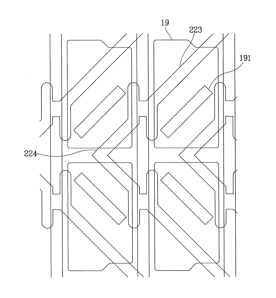
図4は二重パターンマスクで形成された突起の例を示した平面図であって、幅が広い第1突起221及び幅が狭い第2突起222が互いに平行にのびている。図に示したように、第2突起222は第1突起221の両側周辺に存在することもでき、一側周辺にだけ存在することもできる。
FIG. 4 is a plan view showing an example of a protrusion formed of a double pattern mask, in which a
図5は本発明の一実施例による液晶表示装置の配置図である。
図1及び図5に示したように、本発明の一実施例による液晶表示装置の下部表示板1の画素電極19には、斜線状に斜めにのびた切開部191が形成されており、上部表示板2の共通電極27上には、複数の大小の突起223、224が形成されている。各突起223、224は、図4に示したように、高さが高い主突起、及びその周辺に位置して、高さが低い副突起からなる。突起223,224は、異なる方向に延びた複数の直線部分を含んで構成されている。
FIG. 5 is a layout view of a liquid crystal display device according to an embodiment of the present invention.
As shown in FIGS. 1 and 5, the
各突起223、224は、楔型の屈折部及びその両端に連結されている縦部からなる。屈折部はほぼ垂直をなす二つの斜線部からなり、縦部は屈折部から鈍角をなして曲がって画素電極19の縁部とほぼ一致する。
Each of the
大きな突起223の屈折部及び小さな突起224の屈折部の屈折方向は互いに反対であり、大きな突起223の屈折部は画素電極19の一つの幅全体をななめに横切り、小さな突起224の屈折部は画素電極19の一つの幅の半分程度をななめに横切る。
The refraction direction of the refraction part of the large protrusion 223 and the refraction part of the
画素電極19の列方向に沿って見ると、大きな突起223及び小さな突起224が交互に配置されていて、大きな突起223の屈折部及びこれに隣接した小さな突起224の屈折部は互いに平行で、これらの間にはこれらと平行な切開部191が位置する。図5には、隣接した画素電極19の列の大きな突起223の縦部及び小さな突起224の縦部が連結されていることが示されているが、そうでなくて離れていてもよい。
When viewed along the column direction of the
画素電極19の切開部191は突起で代替することができる。
このような切開部191及び突起223、224は、画素電極19及び共通電極27の間に生成される垂直方向の電界に水平方向の成分を形成し、液晶層3の液晶分子が傾く方向を決定する。切開部191及び突起223、224を中心に両側の液晶分子が反対方向に傾き、切開部191及び突起223、224が互いに垂直をなす部分を有するので、液晶分子が全部で四つの方向に傾き、これにより視野角が広くなる。
The
The
一方、前記では共通電極表示板側に遮光膜及び色フィルターが形成されることを例示したが、これらは対向電極基板側でなく画素電極表示板側に形成されることもできる。また、オーバーコート膜は必要に応じて省略することができる。 On the other hand, in the above description, the light shielding film and the color filter are formed on the common electrode panel side. However, they may be formed on the pixel electrode panel side instead of the counter electrode substrate side. Further, the overcoat film can be omitted as necessary.
また、本実施例の場合、共通電極のある共通電極表示板側に突起を形成することを例示したが、画素電極表示板側の画素電極上にこのような二重突起を形成することもできる。
この場合、画素電極上にも同様に図2のマスクパターンを使用して突起を形成して、画素電極側に配向膜を塗布する。
Further, in the present embodiment, it is exemplified that the protrusion is formed on the common electrode display panel side having the common electrode. However, such a double protrusion can be formed on the pixel electrode on the pixel electrode display panel side. .
In this case, protrusions are similarly formed on the pixel electrode using the mask pattern of FIG. 2, and an alignment film is applied to the pixel electrode side.
また、本発明は、画素電極基板及び対向電極基板の全てに突起を形成する方式だけでなく、いずれか一側の基板には突起を形成して他側の基板には他の種類のドメイン形成手段、たとえば開口部を形成する方式にも適用することもできる。 In addition, the present invention is not limited to the method of forming protrusions on all of the pixel electrode substrate and the counter electrode substrate, but forming protrusions on one of the substrates and forming other types of domains on the other substrate. The present invention can also be applied to means for forming an opening, for example.
以上で、実施例を参照して本発明を説明したが、当該技術分野の熟練した当業者は、特許請求の範囲に記載された本発明の思想及び領域から逸脱しない範囲内で、本発明を多様に修正及び変更することができる。 The present invention has been described with reference to the embodiments. However, those skilled in the art will recognize the present invention within the scope and spirit of the present invention described in the claims. Various modifications and changes can be made.
20 マスク
21 第1マスクパターン
22 第2マスクパターン
200 ベース基板
210 電界生成電極(対向電極)
220 配向膜
221 第1突起
222 第2突起
20
220
Claims (19)
前記ベース基板上に形成された少なくとも一つの電界生成電極と、
前記電界生成電極上に形成され、互いに異なる高さを有する第1突起及び第2突起を含む突起部と、
前記突起部上に形成された配向膜と、
を含む、液晶表示装置用表示板。 A base substrate;
At least one electric field generating electrode formed on the base substrate;
A protrusion including a first protrusion and a second protrusion formed on the electric field generating electrode and having different heights;
An alignment film formed on the protrusion,
A display panel for a liquid crystal display device.
前記ゲート線上に形成されたデータ線と、
前記ゲート線、前記データ線及び前記電界生成電極と連結されたスイッチング素子と、
をさらに含む、請求項8に記載の液晶表示装置用表示板。 A plurality of gate lines formed on the base substrate;
A data line formed on the gate line;
A switching element connected to the gate line, the data line, and the electric field generating electrode;
The display panel for a liquid crystal display device according to claim 8, further comprising:
前記電界生成電極上に互いに異なる高さの突起を形成する段階と、
前記突起上に配向膜を形成する段階と、
を含む、液晶表示装置の製造方法。 Forming an electric field generating electrode on the base substrate;
Forming protrusions having different heights on the electric field generating electrode;
Forming an alignment film on the protrusion;
A method for manufacturing a liquid crystal display device, comprising:
前記電界生成電極上に感光材を塗布する段階と、
二重パターンマスクを利用して前記感光材を露光する段階と、
を含む、請求項10に記載の液晶表示装置の製造方法。 Forming the protrusions comprises:
Applying a photosensitive material on the electric field generating electrode;
Exposing the photosensitive material using a double pattern mask;
The manufacturing method of the liquid crystal display device of Claim 10 containing this.
前記第1配線上に第1絶縁膜を形成する段階と、
前記第1絶縁膜上に第2配線を形成する段階と、
前記第2配線上に第2絶縁膜を形成する段階と、をさらに含み、
前記電界生成電極を前記第2絶縁膜上に形成する、請求項11に記載の液晶表示装置の製造方法。 Forming a first wiring on the base substrate;
Forming a first insulating film on the first wiring;
Forming a second wiring on the first insulating film;
Forming a second insulating film on the second wiring; and
The method of manufacturing a liquid crystal display device according to claim 11, wherein the electric field generating electrode is formed on the second insulating film.
第2ベース基板と、前記第2ベース基板上に形成された対向電極と、前記対向電極上に形成され、互いに異なる高さを有する第1突起及び第2突起を含む突起部と、前記突起部上に形成された第2配向膜と、を含む第2基板と、
前記第1基板と前記第2基板との間に介在する液晶層と、
を含む、液晶表示装置。 A first base substrate; a gate line formed on the first base substrate; a data line formed on the gate line; a part of the gate line and a switching element connected to the data line; A first substrate comprising: a pixel electrode electrically connected to a switching element; a domain forming unit formed on the pixel electrode; and a first alignment film formed on the domain forming unit;
A second base substrate; a counter electrode formed on the second base substrate; a protrusion including a first protrusion and a second protrusion formed on the counter electrode and having different heights; and the protrusion A second substrate including a second alignment film formed thereon,
A liquid crystal layer interposed between the first substrate and the second substrate;
A liquid crystal display device.
Applications Claiming Priority (1)
| Application Number | Priority Date | Filing Date | Title |
|---|---|---|---|
| KR1020040022054A KR100984363B1 (en) | 2004-03-31 | 2004-03-31 | Liquid crystal display and fabricating method thereof |
Publications (1)
| Publication Number | Publication Date |
|---|---|
| JP2005292833A true JP2005292833A (en) | 2005-10-20 |
Family
ID=35067499
Family Applications (1)
| Application Number | Title | Priority Date | Filing Date |
|---|---|---|---|
| JP2005102405A Abandoned JP2005292833A (en) | 2004-03-31 | 2005-03-31 | Liquid crystal display device and manufacturing method thereof |
Country Status (5)
| Country | Link |
|---|---|
| US (1) | US7515233B2 (en) |
| JP (1) | JP2005292833A (en) |
| KR (1) | KR100984363B1 (en) |
| CN (1) | CN1680863B (en) |
| TW (1) | TW200606499A (en) |
Families Citing this family (5)
| Publication number | Priority date | Publication date | Assignee | Title |
|---|---|---|---|---|
| US20130183612A1 (en) * | 2010-10-05 | 2013-07-18 | Sharp Kabushiki Kaisha | Method for producing substrate for liquid crystal display panel, and photomask |
| TWI522711B (en) * | 2013-09-12 | 2016-02-21 | 友達光電股份有限公司 | Display device |
| WO2016172857A1 (en) * | 2015-04-28 | 2016-11-03 | 华为技术有限公司 | Multi-domain vertical alignment liquid crystal screen and manufacturing method thereof |
| KR102576995B1 (en) | 2018-07-02 | 2023-09-12 | 삼성디스플레이 주식회사 | Display apparatus and Method for manufacturing the same |
| CN109445246B (en) * | 2019-01-02 | 2022-01-11 | 京东方科技集团股份有限公司 | Mask plate for manufacturing double-domain electrode, double-domain electrode and display panel |
Family Cites Families (17)
| Publication number | Priority date | Publication date | Assignee | Title |
|---|---|---|---|---|
| JP2771392B2 (en) | 1992-06-26 | 1998-07-02 | シャープ株式会社 | Reflective liquid crystal display |
| JPH0784252A (en) | 1993-09-16 | 1995-03-31 | Sharp Corp | Liquid crystal display |
| JPH08185802A (en) * | 1994-12-28 | 1996-07-16 | Noritake Co Ltd | Discharge display device |
| KR100460060B1 (en) | 1996-06-29 | 2005-05-19 | 비오이 하이디스 테크놀로지 주식회사 | Reflective substrate, its manufacturing method and reflective liquid crystal display device |
| JP3284187B2 (en) | 1998-01-29 | 2002-05-20 | シャープ株式会社 | Liquid crystal display device and manufacturing method thereof |
| JP3969887B2 (en) * | 1999-03-19 | 2007-09-05 | シャープ株式会社 | Liquid crystal display device and manufacturing method thereof |
| US6657695B1 (en) * | 1999-06-30 | 2003-12-02 | Samsung Electronics Co., Ltd. | Liquid crystal display wherein pixel electrode having openings and protrusions in the same substrate |
| JP2001141915A (en) | 1999-07-19 | 2001-05-25 | Matsushita Electric Ind Co Ltd | REFLECTIVE PLATE AND METHOD OF MANUFACTURING THE SAME, AND REFLECTIVE DISPLAY ELEMENT PROVIDED WITH THE REFLECTIVE PLATE AND METHOD OF MANUFACTURING THE SAME |
| TW573190B (en) * | 2000-08-14 | 2004-01-21 | Samsung Electronics Co Ltd | Liquid crystal display and fabricating method thereof |
| JP3992922B2 (en) | 2000-11-27 | 2007-10-17 | シャープ株式会社 | LIQUID CRYSTAL DISPLAY SUBSTRATE, ITS MANUFACTURING METHOD, AND LIQUID CRYSTAL DISPLAY DEVICE EQUIPPED WITH THE SAME |
| JP2002328396A (en) * | 2001-04-26 | 2002-11-15 | Nec Corp | Liquid crystal display device and its manufacturing method |
| KR100840538B1 (en) | 2002-03-19 | 2008-06-23 | 엘지디스플레이 주식회사 | Reflective Liquid Crystal Display Manufacturing Method |
| US7248318B2 (en) * | 2002-05-31 | 2007-07-24 | Sharp Kabushiki Kaisha | Liquid crystal display device and method of producing the same |
| JP2005055880A (en) * | 2003-07-24 | 2005-03-03 | Sharp Corp | Liquid crystal display device and driving method thereof |
| KR101016740B1 (en) * | 2003-12-30 | 2011-02-25 | 엘지디스플레이 주식회사 | Liquid crystal display device and manufacturing method thereof |
| JP2007101952A (en) * | 2005-10-05 | 2007-04-19 | Toshiba Matsushita Display Technology Co Ltd | Liquid crystal display |
| JP2007128091A (en) * | 2005-11-03 | 2007-05-24 | Samsung Electronics Co Ltd | Display substrate, manufacturing method thereof, and display panel including the same |
-
2004
- 2004-03-31 KR KR1020040022054A patent/KR100984363B1/en not_active Expired - Fee Related
-
2005
- 2005-03-31 US US11/094,147 patent/US7515233B2/en active Active
- 2005-03-31 CN CN2005100741705A patent/CN1680863B/en not_active Expired - Fee Related
- 2005-03-31 JP JP2005102405A patent/JP2005292833A/en not_active Abandoned
- 2005-03-31 TW TW094110391A patent/TW200606499A/en unknown
Also Published As
| Publication number | Publication date |
|---|---|
| KR20050096617A (en) | 2005-10-06 |
| CN1680863A (en) | 2005-10-12 |
| CN1680863B (en) | 2010-04-28 |
| TW200606499A (en) | 2006-02-16 |
| US7515233B2 (en) | 2009-04-07 |
| US20050231668A1 (en) | 2005-10-20 |
| KR100984363B1 (en) | 2010-09-30 |
Similar Documents
| Publication | Publication Date | Title |
|---|---|---|
| JP5732186B2 (en) | Liquid crystal display | |
| TWI285781B (en) | LCD device | |
| JP5379124B2 (en) | Liquid crystal display | |
| CN101943834B (en) | Liquid crystal display device | |
| US7817239B2 (en) | Liquid crystal display panel and manufacturing method thereof | |
| US8379170B2 (en) | Methods for manufacturing pixel unit, liquid crystal display panel, and electro-optical apparatus | |
| CN100407024C (en) | Liquid crystal display device and manufacturing method thereof | |
| JP2007264231A (en) | Ffs mode liquid crystal display panel | |
| JP4703128B2 (en) | Liquid crystal display | |
| JP4783798B2 (en) | Liquid crystal display device and manufacturing method thereof | |
| WO2009130908A1 (en) | Liquid crystal display device | |
| JP2010169814A (en) | Liquid crystal display device | |
| CN102591059B (en) | Display panel | |
| JP2006267317A (en) | Active matrix liquid crystal display device | |
| CN104040415B (en) | Liquid crystal display device | |
| JP4104885B2 (en) | Liquid crystal display device and manufacturing method thereof | |
| JP5086458B2 (en) | Liquid crystal display device and manufacturing method thereof | |
| US20060072049A1 (en) | Liquid crystal display and thin film transistor array panel usable with the liquid crystal display | |
| US6674501B2 (en) | Cone protrusion in multi-domain vertically aligned liquid crystal display | |
| JP4412494B2 (en) | Multi-domain vertical alignment liquid crystal display panel, thin film transistor array, and manufacturing method thereof | |
| JP2007052264A (en) | Liquid crystal display panel | |
| JP2005292833A (en) | Liquid crystal display device and manufacturing method thereof | |
| JP7313958B2 (en) | Display device manufacturing method | |
| JP2024507036A (en) | Array substrate and liquid crystal display panel | |
| KR20040054246A (en) | In-Plane Switching mode Liquid Crystal Display Device |
Legal Events
| Date | Code | Title | Description |
|---|---|---|---|
| A621 | Written request for application examination |
Free format text: JAPANESE INTERMEDIATE CODE: A621 Effective date: 20080228 |
|
| A762 | Written abandonment of application |
Free format text: JAPANESE INTERMEDIATE CODE: A762 Effective date: 20090519 |