JP2005292742A - Plasma display device - Google Patents
Plasma display device Download PDFInfo
- Publication number
- JP2005292742A JP2005292742A JP2004111804A JP2004111804A JP2005292742A JP 2005292742 A JP2005292742 A JP 2005292742A JP 2004111804 A JP2004111804 A JP 2004111804A JP 2004111804 A JP2004111804 A JP 2004111804A JP 2005292742 A JP2005292742 A JP 2005292742A
- Authority
- JP
- Japan
- Prior art keywords
- plasma display
- magnetic field
- electric field
- display device
- filter
- Prior art date
- Legal status (The legal status is an assumption and is not a legal conclusion. Google has not performed a legal analysis and makes no representation as to the accuracy of the status listed.)
- Pending
Links
Images

Landscapes
- Devices For Indicating Variable Information By Combining Individual Elements (AREA)
- Shielding Devices Or Components To Electric Or Magnetic Fields (AREA)
Abstract
Description
本発明は、大画面で、薄型、軽量のディスプレイ装置として知られているプラズマディスプレイ装置の不要輻射に関するものである。 The present invention relates to unnecessary radiation of a plasma display device known as a thin, lightweight display device having a large screen.
近年、プラズマディスプレイ装置は、視認性に優れた表示パネル(薄型表示デバイス)として注目されており、高精細化および大画面化が進められている。 In recent years, plasma display devices have attracted attention as display panels (thin display devices) with excellent visibility, and higher definition and larger screens are being promoted.
このプラズマディスプレイ装置には、大別して、駆動的にはAC型とDC型があり、放電形式では面放電型と対向放電型の2種類があるが、高精細化、大画面化および製造の簡便性から、現状では、AC型で面放電型のプラズマディスプレイ装置が主流を占めるようになってきている。
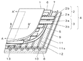
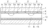
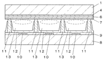
まず、プラズマディスプレイ装置におけるプラズマディスプレイパネルの構造について図3を用いて説明する。 図4に図3のA−A’線で切断した断面を示し、図5に図3のB−B’線で切断した断面を示している。図に示すように、ガラス基板などの透明な前面側の基板1上には、走査電極2と維持電極3とで対をなすストライプ状の表示電極4が複数対形成され、そして基板1上の隣り合う表示電極4間には遮光層5が配置形成されている。この走査電極2および維持電極3は、それぞれ透明電極2a、3aおよびこの透明電極2a、3aに電気的に接続された銀等の母線2b、3bとから構成されている。また、前記前面側の基板1には、前記複数対の電極群を覆うように誘電体層6が形成され、その誘電体層6上には保護膜7が形成されている。
This plasma display device is roughly classified into an AC type and a DC type in terms of driving, and there are two types of discharge types: a surface discharge type and a counter discharge type. Therefore, at present, AC-type and surface-discharge-type plasma display devices are mainly used.
First, the structure of the plasma display panel in the plasma display device will be described with reference to FIG. 4 shows a cross section taken along line AA ′ in FIG. 3, and FIG. 5 shows a cross section taken along line BB ′ in FIG. As shown in the figure, a plurality of pairs of
また、前記前面側の基板1に対向配置される背面側の基板8上には、基板1上の走査電極2及び維持電極3の表示電極4と直交する方向に、絶縁体層9で覆われた複数のストライプ状のデータ電極10が形成されている。このデータ電極10間の絶縁体層9上には、データ電極10と平行にストライプ状の複数の隔壁11が配置され、この隔壁11間の側面11aおよび絶縁体層9の表面に蛍光体層12が設けられている。
Further, an insulating layer 9 is covered on the
これらの基板1と基板8とは、走査電極2および維持電極3とデータ電極10とが直交するように、微小な放電空間を挟んで対向配置されるとともに、周囲が封止され、そして前記放電空間には、例えばヘリウム、ネオン、アルゴン、キセノンなどのうちの一種または混合ガスが放電ガスとして封入されている。また、放電空間は、隔壁11によって複数の区画に仕切ることにより、表示電極4とデータ電極10との交点が位置する複数の放電セル13が設けられ、その各放電セル13には、赤色、緑色及び青色となるように蛍光体層12が一色ずつ順次配置されている。
The
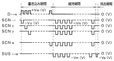
次に、上記パネル本体の動作について説明すると、このパネル本体の電極配列は、図6に示すように、M本×N本(M,Nは整数)の放電セルからなるマトリックス構成であり、行方向にはM行の走査電極SCN1〜SCNMおよび維持電極SUS1〜SUSMが配列され、列方向にはN列のデータ電極D1〜DNが配列されている。 Next, the operation of the panel body will be described. The electrode arrangement of the panel body has a matrix configuration composed of M × N discharge cells (M and N are integers) as shown in FIG. M rows of scan electrodes SCN1 to SCNM and sustain electrodes SUS1 to SUSM are arranged in the direction, and N columns of data electrodes D1 to DN are arranged in the column direction.
また、このパネル本体を用いたAC型プラズマディスプレイ装置の駆動方法のタイミングチャートの一例を図7に示す。 FIG. 7 shows an example of a timing chart of a driving method of an AC type plasma display device using this panel body.
図6および図7に示すように、書き込み期間では、全ての維持電極SUS1〜SUSMを0ボルト(V)に保持した後に、第1行目の表示する放電セルに対応する所定のデータ電極D1〜DNに正の書き込みパルス電圧+Vw(V)を、第1行目の走査電極SCN1に負の走査パルス電圧−Vs(V)をそれぞれに印加すると、所定のデータ電極D1〜DNと第1行目の走査電極SCN1との交点部において、書き込み放電が起こる。 As shown in FIGS. 6 and 7, in the write period, after all the sustain electrodes SUS1 to SUSM are held at 0 volts (V), predetermined data electrodes D1 to D1 corresponding to the discharge cells to be displayed in the first row are displayed. When a positive write pulse voltage + Vw (V) is applied to DN and a negative scan pulse voltage -Vs (V) is applied to the scan electrode SCN1 in the first row, the predetermined data electrodes D1 to DN and the first row are applied. Write discharge occurs at the intersection with the scan electrode SCN1.
次に、第2行目の表示する放電セルに対応する所定のデータ電極D1〜DNに正の書き込みパルス電圧+Vw(V)を、第2行目の走査電極SCN2に負の走査パルス電圧−Vs(V)をそれぞれに印加すると、所定のデータ電極D1〜DNと第2行目の走査電極SCN2との交点部において書き込み放電が起こる。 Next, positive write pulse voltage + Vw (V) is applied to predetermined data electrodes D1 to DN corresponding to discharge cells to be displayed in the second row, and negative scan pulse voltage -Vs is applied to scan electrode SCN2 in the second row. When (V) is applied to each, an address discharge occurs at the intersection of predetermined data electrodes D1 to DN and scan electrode SCN2 in the second row.
上記同様の動作が順次に行われて、最後に第M行目の表示する放電セルに対応する所定のデータ電極D1〜DNに正の書き込みパルス電圧+Vw(V)を、第M行目の走査電極SCNMに負の走査パルス電圧−Vs(V)をそれぞれに印加すると、所定のデータ電極D1〜DNと第M行目の走査電極SCNMとの交点部において書き込み放電が起こる。 The same operation as described above is sequentially performed. Finally, a positive write pulse voltage + Vw (V) is applied to predetermined data electrodes D1 to DN corresponding to discharge cells to be displayed in the Mth row, and the Mth row is scanned. When a negative scan pulse voltage −Vs (V) is applied to each electrode SCNM, an address discharge occurs at the intersection of predetermined data electrodes D1 to DN and the Mth scan electrode SCNM.
次の維持期間では、全ての走査電極SCN1〜SCNMを一旦0(V)に保持すると共に、全ての維持電極SUS1〜SUSMに負の維持パルス電圧−Vm(V)を印加すると、書き込み放電を起こした前記交点部における走査電極SCN1〜SCNMと維持電極SUS1〜SUSMとの間に維持放電が起こる。次に全ての走査電極SCN1〜SCNMと全ての維持電極SUS1〜SUSMとに負の維持パルス電圧−Vm(V)を交互に印加することにより、表示する放電セルにおいて維持放電が継続して起こる。この維持放電の発光によりパネル表示が行われる。 In the next sustain period, all the scan electrodes SCN1 to SCNM are temporarily held at 0 (V), and when a negative sustain pulse voltage −Vm (V) is applied to all the sustain electrodes SUS1 to SUSM, an address discharge is caused. In addition, a sustain discharge occurs between scan electrodes SCN1 to SCNM and sustain electrodes SUS1 to SUSM at the intersections. Next, by applying negative sustain pulse voltage −Vm (V) alternately to all scan electrodes SCN1 to SCNM and all sustain electrodes SUS1 to SUSM, sustain discharge continuously occurs in the display discharge cells. Panel display is performed by the light emission of the sustain discharge.
次の消去期間において、全ての走査電極SCN1〜SCNMを一旦0(V)に保持すると共に、全ての維持電極SUS1〜SUSMに消去パルス電圧−Ve(V)を印加すると、消去放電を起こして放電が停止する。 In the next erasing period, all the scan electrodes SCN1 to SCNM are temporarily held at 0 (V), and when the erasing pulse voltage −Ve (V) is applied to all the sustain electrodes SUS1 to SUSM, an erasing discharge is caused to cause a discharge. Stops.
以上の動作により、AC型プラズマディスプレイ装置において、一画面が表示される。 Through the above operation, one screen is displayed in the AC type plasma display apparatus.
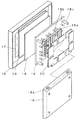
図8に上記で説明したパネル本体を組み込んだプラズマディスプレイ装置の全体構成の一例を示している。図において、パネル本体14を収容するケースは、金属製のフロントケース部15とバックケース部16とから構成され、フロントケース部15の前面にはガラス等からなる透光部17が設けられている。さらに、バックケース部16には、パネル本体14等で発生した熱を外部に放出するための複数の通気孔16aが設けられている。
FIG. 8 shows an example of the overall configuration of a plasma display device incorporating the panel body described above. In the figure, a case for housing the
前記パネル本体14は、アルミニウム製のシャーシ部材18の前面に絶縁性の熱伝導シート19を介して接着することにより保持され、そしてシャーシ部材18の後面側には、パネル本体14を発光駆動させるための複数の回路ブロック20が取り付けられている。前記熱伝導シート19は、パネル本体14で発生した熱をシャーシ部材18に効率よく伝え、放熱を行うためのものであり、回路ブロック20はパネル本体14の発光駆動とその制御を行うための電気回路を備えており、パネル本体14の縁部に引き出された電極引出部に、シャーシ部材18の四辺の縁部を越えて延びる複数のフレキシブル配線基板(図示せず)によって電気的に接続されている。
The
また、シャーシ部材18の後面には、複数の放熱用フィン18aと回路ブロック20を取り付けるための複数のボス部18bとシャーシ部材18をバックケース部16に固定するためのボス部18cとが、ダイカストや鋳造等による一体成型により突設されている。
(たとえば、特許文献1参照)。
Further, on the rear surface of the
(For example, refer to Patent Document 1).
以上のような構成を持つプラズマディスプレイ装置において、維持期間において走査電極と維持電極の一組に約400mAp−pの電流が流れるのでM行の電極がある場合
0.4Ap−p×M=0.4M Ap−p
となり、例えばMを480本とすれば192Ap−pの放電電流が流れる。 よって約192Ap−pの電流により引き起こされる電磁波妨害は重要な課題である。
In the plasma display device having the above-described configuration, a current of about 400 mAp-p flows through one set of the scan electrode and the sustain electrode in the sustain period, and therefore, when there are M rows of electrodes, 0.4 Ap-p × M = 0. 4M Ap-p
For example, if M is 480, a discharge current of 192 Ap-p flows. Therefore, electromagnetic interference caused by a current of about 192 Ap-p is an important issue.
さらに電磁波は、計器に障害を及ぼすことが知られており、最近では、電磁波が人体にも障害を及ぼす可能性もあるとの報告もされている。このため、電磁波放出に関しては、法的に規制される方向になっている。例えば、現在日本では、VCCI(Voluntaly Control Council for Interference by data processing equipment electronic office machine)による規制があり、米国では、FCC(Federal Communication Commission)による製品規制がある。以上のような電磁波妨害については、電磁波遮断フィルターが、電磁波遮断用途としてテレビやコンピューター用CRTモニターに広く用いられている。 Furthermore, electromagnetic waves are known to cause damage to instruments, and recently it has been reported that electromagnetic waves may also damage the human body. For this reason, the electromagnetic wave emission is in a legally regulated direction. For example, in Japan, there is a regulation by VCCI (Voluntary Control Council for Interference by data processing equipment electronic machinery machine), and in the United States by FCC (Federal Communications). Regarding electromagnetic interference as described above, electromagnetic wave shielding filters are widely used for televisions and computer CRT monitors as electromagnetic wave shielding applications.
たとえば、特許文献2においてプラズマディスプレイパネル(PDP)は、その発光原理上強度の電磁波を表示部分から外部に放出する強度の電磁波を遮断するためには、低抵抗であり透明な電磁波遮断フィルターが必要であると述べられている。
For example, in
上記特許文献2には、低抵抗透明導電性薄膜の開発にあたっては、金属薄膜層、特に純物質中で最も比抵抗が小さい銀を用いた金属薄膜層の利用が有効であり、さらに透過率上昇及び金属薄膜層の安定性向上の目的で、金属薄膜層を透明高屈折率薄膜層で挟み込み透明導電性薄膜積層体を形成することが非常に効果的であり、この透明導電性薄膜積層体は、各薄膜層の材料や膜厚を選ぶことによって、用途に応じて最適な光学特性及び電気特性を持つように設計することができると提案されている。
In the above-mentioned
さらに上記特許文献2には、金属薄膜層材料としてその比抵抗の低さ故に好適に用いられる銀は、反面原子の凝集を生じやすいという面を持つ。例えば、塩化物イオン存在下又は、電場下において容易に凝集を生じる。銀薄膜中の銀原子が凝集すると銀白色の点を生じ、本来持つ高透明性や、低抵抗性を失ってしまう。銀の凝集を抑制するための手法の1つとして、銀を合金化する方法がある。合金化に用いる金属としては、金、銅、パラジウムが一般的である。従来は銀とパラジウムと銅からなる合金が最も耐久性の優れた銀合金材料であった。特にパラジウム及び銅をそれぞれ1重量パーセントずつ含有する銀合金を用いた場合は純銀を用いた場合に比較して高透明性及び低抵抗性を著しく損なうこと無く、透明導電性薄膜積層体の耐久性を向上させることができる。
Further, in
しかしながら、これら透明導電性薄膜積層体は、塩化物イオンの存在下において、又は電流を流すことによって銀薄膜層での銀原子の凝集を生じ易い。そのため透明電極や電磁波遮断フィルター用部材として用いた場合に、銀凝集による点状欠陥が生じやすかったとも述べられている。
前記従来の構成ではパネル本体から放出される電磁波を低導電率を有する金属体で低減させることが課題となっていたが、上記のようにプラズマディスプレイ装置のパネル内部では約200Ap−pのピーク交番電流が常時流れるために単純に電磁波を低減すると言うよりも電界、磁界と分離して低減する必要性が発生した。 さらに電磁波を低減するために前面ガラスに銅や銀を利用した電磁波フィルターが導入されているが銅や銀は非磁性体であるので不要電界成分に関しては十分な効果のある遮蔽体になるが、磁界に関しては銅や銀の非磁性体金属に交番磁界が交差したときに銅や銀の非磁性体金属内部で発生する渦電流による外部高周波磁界打消し効果しか期待出来ず、低域磁界成分により発生する磁界不要輻射成分の低減が課題となってきている。 In the conventional configuration, it has been a problem to reduce the electromagnetic wave emitted from the panel body with a metal body having a low conductivity. However, as described above, a peak alternation of about 200 Ap-p is generated inside the panel of the plasma display device. Since current always flows, there is a need to separate and reduce electromagnetic waves rather than simply reducing electromagnetic waves. In order to further reduce electromagnetic waves, an electromagnetic wave filter using copper or silver has been introduced to the front glass, but copper and silver are non-magnetic materials, so it becomes a shield with sufficient effect for unnecessary electric field components, As for the magnetic field, when an alternating magnetic field crosses a copper or silver nonmagnetic metal, only an external high frequency magnetic field canceling effect due to an eddy current generated inside the copper or silver nonmagnetic metal can be expected. Reduction of the generated magnetic field unnecessary radiation component has been an issue.
本発明はこのような課題を解決し、パネル本体からの電界と磁界を低減させることを目的とするものである。 An object of the present invention is to solve such problems and to reduce an electric field and a magnetic field from a panel body.
上記目的を達成するために本発明のプラズマディスプレイ装置は、前面ガラス板の前面側に光学フィルタを設けてなるカラー表示用プラズマディスプレイパネルにおいて、前記光学フィルターにコントラスト改善のために一定範囲の可視光を吸収するとともに、前記カラー表示用プラズマディスプレイパネルで発生する不要電界と不要磁界を吸収する電界・磁界吸収層において強磁性を有する金属メッシュで構成したものである。 In order to achieve the above object, a plasma display device according to the present invention is a color display plasma display panel in which an optical filter is provided on the front side of a front glass plate. And an unnecessary electric field generated in the plasma display panel for color display and an electric field / magnetic field absorbing layer that absorbs an unnecessary magnetic field are made of a metal mesh having ferromagnetism.
本構成により、強磁性を有する金属メッシュを用いるので電界吸収は勿論のこと、非磁性体における渦電流の外部磁界打消し効果は非磁性体金属に劣る(銅や銀のような非磁性を有する金属に比較して導電率が大きい)が、強磁性を有する金属体の磁界遮断効果によりカラー表示用プラズマディスプレイパネルで発生する不要輻射電界と特に不要輻射磁界の吸収を図ることが出来る。 With this configuration, a metal mesh having ferromagnetism is used, so electric field absorption as well as eddy current external magnetic field cancellation effect in nonmagnetic materials are inferior to nonmagnetic metals (having nonmagnetic properties such as copper and silver) However, it is possible to absorb unnecessary radiant electric fields and particularly unnecessary radiant magnetic fields generated in the plasma display panel for color display due to the magnetic field shielding effect of the metal body having ferromagnetism.
また本発明のプラズマディスプレイ装置は、バックカバーの内側に、前記カラー表示用プラズマディスプレイパネルで発生する不要電界と不要磁界を吸収する電界・磁界吸収層において強磁性を有する金属メッシュで構成したフィルタを備えたものであり、本構成によりカラー表示用プラズマディスプレイパネルで発生する不要輻射電界と特に不要輻射磁界の吸収を図り、不要輻射対策に特段の効果を奏するものである。 In the plasma display device of the present invention, a filter formed of a metal mesh having ferromagnetism in an electric field / magnetic field absorption layer that absorbs an unnecessary electric field and an unnecessary magnetic field generated in the color display plasma display panel is provided inside the back cover. With this configuration, it is possible to absorb unnecessary radiation electric field and particularly unwanted radiation magnetic field generated in the plasma display panel for color display, and to achieve a special effect for countermeasures against unwanted radiation.
本発明のプラズマディスプレイ装置によれば、強磁性体の金属をフィルターとして使用するので、不要電界成分に対しては金属本来の低抵抗性により低減が図れ、さらに不要磁界成分に対しては、金属の強磁性により低減が図れるので、プラズマディスプレイ装置の周囲への電界・磁界の不要輻射を低減できる。 According to the plasma display device of the present invention, since a ferromagnetic metal is used as a filter, it is possible to reduce unnecessary electric field components by the inherent low resistance of the metal, and for unnecessary magnetic field components, metal Therefore, unnecessary radiation of electric and magnetic fields to the periphery of the plasma display device can be reduced.
以下、本発明を実施するための最良の形態について、図面を参照しながら説明する。 The best mode for carrying out the present invention will be described below with reference to the drawings.
(実施の形態1)
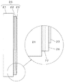
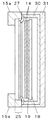
図1は本発明の実施の形態1におけるプラズマディスプレイ用光学フィルター付き前面電界・磁界フィルター25の断面図である。プラズマディスプレイ装置の全体構成の分解斜視図(図8)において、透光部17の表面上でプラズマパネル側に光学フィルター付き前面電界・磁界フィルター25は貼り付けられている。
(Embodiment 1)
FIG. 1 is a cross-sectional view of a front electric field /
プラズマディスプレイ装置の一連の駆動動作は前述した通りで、一画面を表示するのにプラズマディスプレイパネルを構成する複数の電極に電流が流れることによって実現されている。 As described above, a series of driving operations of the plasma display device is realized by flowing current through a plurality of electrodes constituting the plasma display panel in order to display one screen.
ここで、このプラズマディスプレイ装置においては、光学フィルター付き電界・磁界フィルター17に電界・磁界シールドのために、強磁性体の金属メッシュを施し、その強磁性体金属メッシュの周辺部をアースすることにより、プラズマディスプレイパネル前面側から電界・磁界が放出されるのを防いでいる。
Here, in this plasma display device, a ferromagnetic metal mesh is applied to the electric field /
図1において、光学フィルター付き前面電界・磁界フィルター光学フィルター25は光学フィルター(もしくは保護シート)21のパネル本体14側に強磁性を有する金属メッシュ22を形成し、さらにその上に(接して)保護シート23が形成されている。また、強磁性を有する金属メッシュ22の周辺部分には保護シート23が形成されておらず、図1の接続部26でアースを取る構造になっている。
In FIG. 1, a front electric field / magnetic field filter
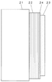
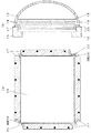
次に図9を用いてプラズマディスプレイ用光学フィルター付き前面電界・磁界フィルター25の固定方法について説明する。図9(a)はプラズマディスプレイパネル14側から見たプラズマディスプレイ用光学フィルター付き前面電界・磁界フィルター25であり、図9(b)はプラズマディスプレイ装置の側面から見た断面図である。
Next, a method for fixing the front surface electric field /
図9(a)の保護シート23は図1で説明した通り、強磁性体の金属メッシュ22の周辺部を残して強磁性体の金属メッシュ22に接して設けられている。保護シート23が設けられなかった領域は、接続部26として、光学フィルター付き前面電界・磁界フィルター25の押え金具27が設けられている。この押え金具27は金属製のものからなり、フロントケース部15に一端が固定され、もう一端で光学フィルター付き前面電界・磁界フィルター25を固定している。
The
図9では、光学フィルター付き前面電界・磁界フィルター25の四辺すべてを押え金具27で固定しているが必ずしもその必要はなく、対向する二辺だけであっても良い。
In FIG. 9, all four sides of the front electric field /
押え金具27は光学フィルター付き前面電界・磁界フィルター25の強磁性の金属メッシュ22と電気的に導通しており、この強磁性の金属メッシュ22は押え金具27を通じてアースされている。
The presser fitting 27 is electrically connected to the
金属メッシュ22は、例えば鉄やニッケル、または鉄合金のような強磁性体のものからなり、光学フィルター21の上に、メッシュ状態に形成されている。
The
以上の構成により、本実施の形態のプラズマディスプレイ装置は、光学フィルター付き前面電界・磁界フィルター光学フィルター25は、外光の反射を抑えるなどの光の制御を行うとともに、プラズマディスプレイパネルから発生される電界や磁界を吸収し、プラズマディスプレイ装置の前面から放射される不要な電磁波を抑えることを可能とするものである。
With the above configuration, in the plasma display device of this embodiment, the front electric field / magnetic field filter
なお、本実施の形態のプラズマディスプレイ装置では、光学フィルター付き前面電界・磁界フィルター光学フィルターとしてプラズマディスプレイパネルから発せられる電界・磁界を防ぐ構成を一例として説明したが、プラズマディスプレイパネルから発せられる不要輻射が装置の外部に放射されるのを低減するという課題に対しては、強磁性体からなるフィルターをプラズマディスプレイパネルの前面側に配置するものであれば、その目的において前述の光学フィルター付き前面電界・磁界フィルター光学フィルターと同等の効果を奏する。 In the plasma display device of the present embodiment, the front electric field / magnetic field filter optical filter with an optical filter has been described as an example of a configuration that prevents an electric field / magnetic field emitted from the plasma display panel. However, unnecessary radiation emitted from the plasma display panel is described. If the filter made of a ferromagnetic material is arranged on the front side of the plasma display panel, the front electric field with an optical filter described above is used for that purpose.・ Magnetic filter Equivalent effect to optical filter.
また、強磁性体からなる金属メッシュ22のかわりに、強磁性体の金属をスパッタによって形成したフィルターで置き換えても、同等の効果を奏することができる。
(実施の形態2)
図2は、本発明の第2の実施の形態の説明図である。図2において図1と同じ構成要素に関しては同じ符号を使用し説明を省略する。
The same effect can be obtained by replacing the
(Embodiment 2)
FIG. 2 is an explanatory diagram of the second embodiment of the present invention. In FIG. 2, the same components as those in FIG.
図2において、強磁性を有する金属メッシュ22の上に(接して)、金属メッシュ22より導電率の低い金属めっき24を施している。さらに金属めっき24の上に(接して)保護シート23が備えられている。保護シート23は、例えば、金属メッシュ22が鉄により構成され、金属めっき24が銀から構成されている。
In FIG. 2, a
このような構成をとることで、電界フィルターとしての電界・磁界に対するシールド効果の向上を図るとともに、光学フィルター付き電界・磁界フィルター25の金属めっき24上において渦電流が増加するので、磁界打消しがさらに向上させることができるものである。
(実施の形態3)
次に、本発明の第3の実施の形態について説明する。(実施の形態1)、(実施の形態2)では、主にプラズマディスプレイ装置の前面から放射される電界または磁界を防ぐための構成について説明したが、プラズマディスプレイ装置からは前面のみならず後面からも放射される電界や磁界は存在するため、これらの電界や磁界をシールドするための構成例を説明する。
By adopting such a configuration, the shielding effect against the electric field / magnetic field as an electric field filter is improved, and eddy currents increase on the metal plating 24 of the electric field /
(Embodiment 3)
Next, a third embodiment of the present invention will be described. In (Embodiment 1) and (Embodiment 2), the configuration for mainly preventing the electric field or magnetic field radiated from the front surface of the plasma display device has been described. However, from the plasma display device, not only from the front surface but also from the rear surface. Since there are electric and magnetic fields that are radiated, a configuration example for shielding these electric and magnetic fields will be described.
図10は、プラズマディスプレイ装置の側面から見た図であり、(実施の形態1)で説明した図9(b)と符号が同じものは同じ構成、動作を行うものである。 FIG. 10 is a view as seen from the side of the plasma display device. Components having the same reference numerals as those in FIG. 9B described in the first embodiment perform the same configuration and operation.
光学フィルター付き前面電界・磁界フィルター25は、その周囲を押え金具27によってフロントケース15に押えられて固定されている。光学フィルター付き前面電界・磁界フィルター25は詳細を記載していないが、図1のように光学フィルター21、金属メッシュ22、および保護シート23からなる構成であってもよく、また図2のように光学フィルター21、金属メッシュ22、低送電率金属めっき24、および保護シート23からなる構成であってもよい。
The front electric field /
プラズマディスプレイパネル14は、前面ガラス基板と後面ガラス基板が張り合わされて構成され、その後面ガラス基板は熱伝導性シート19を介してシャーシ部材18に固定されている。前面ガラス基板は光学フィルター付き前面電界・磁界フィルター25と対面する位置に設けられ、プラズマディスプレイパネル14の前面ガラス基板側から放射される電界・磁界は主に前面ガラス基板は光学フィルター付き前面電界・磁界フィルター25によって吸収され、プラズマディスプレイ装置の外に放射されるのを抑えている。
The
バックケース部31はフロントケース部15に接続されて設けられ、前面ガラス基板は光学フィルター付き前面電界・磁界フィルター25とフロントケース部15とバックケース部31によって、プラズマディスプレイパネル14やシャーシ部材18を囲っている。また図示していないが、シャーシ部材18の後面側には、プラズマディスプレイパネル14を駆動するための回路基板が固定されており、この回路基板からの信号によってプラズマディスプレイパネル14の各画素の発光制御がなされている。
The
バックケース部31の内面側には、電界・磁界フィルター30が設けられている。この電界・磁界フィルター30は、例えば繊維生地の表面に、強磁性体、例えば鉄、ニッケル、フェライトなど、をメッシュ、またはスパッタしたものから構成されている。バックケース部31の内面側に電界・磁界フィルター30が貼られている。この電界・磁界フィルター30は押え金具27と電気的に接続されており、アースされている。
An electric field /
本実施例の構成により、プラズマディスプレイパネル14から放射される電界・磁界が、プラズマディスプレイ装置から放射されるのを抑えることができる。また本実施の形態のように、前面ガラス基板は光学フィルター付き前面電界・磁界フィルター25とともに使用することにより、フロントケース部15およびバックケース部31からの電界・磁界など不要輻射を抑えることを可能にしたものであるが、単独で用いられてもよい。
With the configuration of the present embodiment, it is possible to suppress the electric field / magnetic field radiated from the
また、電界・磁界フィルター30は、バックケース部31の内側に貼り付けられる物でなくてもよく、シャーシ部材18に固定される回路基板毎にそれを覆うように備えられてもよい。
In addition, the electric field /
本実施の形態の構成によれば、プラズマディスプレイパネル14から発射・放射される電界、磁界による電磁波を、周囲に備える電界・磁界フィルター30によって吸収することでプラズマディスプレイ装置から外にでる量を抑えるのに効果がある。従ってこの実施の形態例によりプラズマディスプレイ装置からの不要輻射を減らすことで、周囲の機器の動作に悪影響を与えることなくプラズマディスプレイ装置を動作させることができる。
According to the configuration of the present embodiment, the amount of the electric field emitted from the
また、本実施の形態において電界・磁界フィルター30の構成を繊維生地の表面に強磁性体を付着した例を示したがこの構成に限るものでなく、プラズマディスプレイパネル14の後ろ側に電界・磁界フィルター30と似たような構成のものを備えたものでも同等の効果を得ることができる。例えば、バックケース部31上に、例えば鉄、ニッケル、フェライトなどの強磁性体をメッシュ、またはスパッタして設けたものであってもよい。
In the present embodiment, the configuration of the electric field /
さらには、バックケース部31が強磁性体から作られたものであれば電界・磁界フィルター30と同等の効果をあげることができ、電界・磁界フィルター30をあえて備える必要がない。強磁性体からなるバックケース部31がフロントケース部15と接続されて備えられ、アースされていることで、不要輻射を減らすことが可能である。またこの場合、電界・磁界フィルター30がプラズマディスプレイパネル14とバックケース部31で必要ないため、プラズマディスプレイ装置の内部の空間をより狭くすることができる。
Furthermore, if the
本発明にかかるプラズマディスプレイ装置は、強磁性を有する金属のメッシュフィルターを利用するので、不要電界吸収は勿論のこと特に不要磁界吸収に関して優れた吸収特性を持つので、映像表示を行う光学フィルター付きプラズマディスプレイ装置として不要輻射を低減するプラズマディスプレイ装置として大変有用である。 Since the plasma display device according to the present invention uses a metal mesh filter having ferromagnetism, the plasma display device has an excellent absorption characteristic with respect to unnecessary magnetic field absorption as well as unnecessary electric field absorption. It is very useful as a plasma display device for reducing unnecessary radiation as a display device.
1 前面側の基板
2 走査電極
3 維持電極
4 表示電極
5 遮光層
6 誘電体層
7 保護膜
8 背面側の基板
9 絶縁体層
10 データ電極
11 隔壁
12 蛍光体層
13 放電セル
14 パネル本体
15 フロントケース部
16、31 バックケース部
17 透光部
18 シャーシ部材
19 熱伝導シート
20 回路ブロック
21 光学フィルター(もしくは保護シート)
22 強磁性を有する金属メッシュ
23 保護シート
24 低導電率金属めっき
25 光学フィルター付き前面電界・磁界フィルター
26 接続部
27 押え金具
30 電界・磁界フィルター
DESCRIPTION OF
21 Optical filter (or protective sheet)
22 Metal
Claims (7)
Priority Applications (1)
| Application Number | Priority Date | Filing Date | Title |
|---|---|---|---|
| JP2004111804A JP2005292742A (en) | 2004-04-06 | 2004-04-06 | Plasma display device |
Applications Claiming Priority (1)
| Application Number | Priority Date | Filing Date | Title |
|---|---|---|---|
| JP2004111804A JP2005292742A (en) | 2004-04-06 | 2004-04-06 | Plasma display device |
Publications (1)
| Publication Number | Publication Date |
|---|---|
| JP2005292742A true JP2005292742A (en) | 2005-10-20 |
Family
ID=35325690
Family Applications (1)
| Application Number | Title | Priority Date | Filing Date |
|---|---|---|---|
| JP2004111804A Pending JP2005292742A (en) | 2004-04-06 | 2004-04-06 | Plasma display device |
Country Status (1)
| Country | Link |
|---|---|
| JP (1) | JP2005292742A (en) |
Cited By (3)
| Publication number | Priority date | Publication date | Assignee | Title |
|---|---|---|---|---|
| KR100861245B1 (en) * | 2007-04-25 | 2008-10-02 | 엘지전자 주식회사 | Display filter, manufacturing method for manufacturing the same and display device including the same |
| CN112053629A (en) * | 2019-06-05 | 2020-12-08 | 株式会社日本有机雷特显示器 | Display device and method of manufacturing the same |
| CN114184900A (en) * | 2021-11-04 | 2022-03-15 | 中国工程物理研究院应用电子学研究所 | Strong electric field breakdown monitoring system for micro-area enclosed space |
-
2004
- 2004-04-06 JP JP2004111804A patent/JP2005292742A/en active Pending
Cited By (3)
| Publication number | Priority date | Publication date | Assignee | Title |
|---|---|---|---|---|
| KR100861245B1 (en) * | 2007-04-25 | 2008-10-02 | 엘지전자 주식회사 | Display filter, manufacturing method for manufacturing the same and display device including the same |
| CN112053629A (en) * | 2019-06-05 | 2020-12-08 | 株式会社日本有机雷特显示器 | Display device and method of manufacturing the same |
| CN114184900A (en) * | 2021-11-04 | 2022-03-15 | 中国工程物理研究院应用电子学研究所 | Strong electric field breakdown monitoring system for micro-area enclosed space |
Similar Documents
| Publication | Publication Date | Title |
|---|---|---|
| US7321186B2 (en) | Front filter, and plasma display apparatus having the same | |
| JPH10282896A (en) | Display device | |
| US8072778B2 (en) | Plasma display device | |
| JP3289684B2 (en) | Plasma display panel, plasma display module and driving method thereof | |
| JP2004004706A (en) | Plasma display device | |
| JP2005292742A (en) | Plasma display device | |
| JP2009251065A (en) | Plasma display | |
| JP3953362B2 (en) | Electrical equipment with cable | |
| KR100669785B1 (en) | Plasma display module | |
| EP1696455B1 (en) | Structure for stabilizing drive pulses and plasma display device using the same | |
| JP5197793B2 (en) | Display device | |
| US7791277B2 (en) | Plasma display panel provided with grounding units for the assembly of the display panel and an electromagnetic interference shielding flim | |
| JP2010010255A (en) | Electromagnetic wave shield member | |
| JP2004069888A (en) | Plasma display device | |
| US20090231238A1 (en) | Plasma display device | |
| JP4786037B2 (en) | Display device | |
| KR100412085B1 (en) | Plasma display device | |
| JP2005326443A (en) | Plasma display device | |
| JP2009223003A (en) | Plasma display device | |
| KR100669791B1 (en) | Plasma display module | |
| JP2009223002A (en) | Plasma display device | |
| JP2002163991A (en) | Plasma display module | |
| JP2009223004A (en) | Plasma display device | |
| JP2009251422A (en) | Plasma display | |
| JP3925323B2 (en) | Plasma display device |