JP2005291999A - Strain gauge equipped with a chip with wireless function - Google Patents
Strain gauge equipped with a chip with wireless function Download PDFInfo
- Publication number
- JP2005291999A JP2005291999A JP2004109167A JP2004109167A JP2005291999A JP 2005291999 A JP2005291999 A JP 2005291999A JP 2004109167 A JP2004109167 A JP 2004109167A JP 2004109167 A JP2004109167 A JP 2004109167A JP 2005291999 A JP2005291999 A JP 2005291999A
- Authority
- JP
- Japan
- Prior art keywords
- strain
- strain gauge
- chip
- gauge
- deformation
- Prior art date
- Legal status (The legal status is an assumption and is not a legal conclusion. Google has not performed a legal analysis and makes no representation as to the accuracy of the status listed.)
- Pending
Links
Images


Landscapes
- Measurement Of Length, Angles, Or The Like Using Electric Or Magnetic Means (AREA)
- Arrangements For Transmission Of Measured Signals (AREA)
- Testing Of Devices, Machine Parts, Or Other Structures Thereof (AREA)
Abstract
【課題】大型構造物、建築物の変形状態や高速回転構造体の回転中の変形状態を、煩雑な配線処理を施すことなく、正確に実行可能な無線機能付チップを搭載したひずみゲージを実現する。
【解決手段】ひずみ感応ゲージ部1と、無線送受信アンテナ4と、ひずみ感応ゲージ部1により検出された対象物のひずみ値をアンテナ4を介して無線発信する無線機能付チップ3とを備える。測定対象物の変形情報を無線で送信できるので、大型構造物の変形状態や高速回転構造体の回転中の変形状態を煩雑な配線処理を施すことなく正確に実行できる。無線機能付チップ3を有するひずみゲージを橋梁等の構造物に複数箇所備え付け、複数箇所から構造体変形情報を入手すれば、振動時の変形量、変形箇所と、振動がないときの変形量、変形箇所とを比較して解析して構造体の安全性確認や強度の低下予測等を行うことも可能となる。
【選択図】 図1[PROBLEMS] To realize a strain gauge equipped with a chip with a wireless function that can accurately execute deformation states of large structures and buildings and deformation states during rotation of high-speed rotating structures without performing complicated wiring processing. To do.
A strain sensitive gauge unit, a wireless transmission / reception antenna, and a chip with a wireless function for wirelessly transmitting a strain value of an object detected by the strain sensitive gauge unit through the antenna. Since the deformation information of the measurement object can be transmitted wirelessly, the deformation state of the large structure and the deformation state during rotation of the high-speed rotation structure can be accurately executed without performing complicated wiring processing. If a strain gauge having a wireless function chip 3 is provided at a plurality of locations on a structure such as a bridge and the structure deformation information is obtained from the plurality of locations, the deformation amount during vibration, the deformation location, and the deformation amount when there is no vibration, It is also possible to confirm the safety of the structure, predict strength reduction, and the like by comparing and analyzing the deformed portion.
[Selection] Figure 1
Description
本発明は、構造物の応力やひずみを測定するひずみゲージに関する。 The present invention relates to a strain gauge that measures stress and strain of a structure.
ひずみゲージを用いて、構造物のひずみを測定する場合には、ゲージ部が形成されたテープ基材領域を測定エリアに接着剤を用いて貼り付ける。そして、ゲージ部から引き出された配線をブリッジ回路に結線し、ゲージ部分の抵抗変化に伴う微小電圧変化を、別途接続されたストレインアンプで増幅することによって応力やひずみが計測される。 When measuring the strain of a structure using a strain gauge, the tape base material region in which the gauge portion is formed is attached to the measurement area using an adhesive. The wiring drawn from the gauge part is connected to a bridge circuit, and a minute voltage change accompanying a resistance change in the gauge part is amplified by a separately connected strain amplifier to measure stress and strain.
ひずみゲージを用いて構造物のひずみ測定を行う場合、測定対象物の変形による出力だけでなく、特に温度変化を伴う場合には、測定ゲージ自身の導体抵抗変化や被着材との熱膨張差による出力も併せて計測される。このため、通常、アクティブダミーゲージ法と言って、別のひずみゲージを被測定物と同一のサンプルに貼り付けて温度補償を行う必要がある。 When measuring strain of a structure using a strain gauge, not only the output due to deformation of the object to be measured, but also when there is a change in temperature, the change in conductor resistance of the measurement gauge itself and the difference in thermal expansion from the substrate The output by is also measured. For this reason, normally, it is necessary to perform temperature compensation by attaching another strain gauge to the same sample as the object to be measured, called the active dummy gauge method.
しかし、上記アクティブダミーゲージ法においては、実際の変形を測定するひずみ感応ゲージと、温度補償を行うダミーゲージの位置とが離れた部位にあることや、抵抗素材の不均一性のために完全な温度補償を行うことができなかった。 However, in the above active dummy gauge method, the strain sensitive gauge that measures the actual deformation and the dummy gauge that performs the temperature compensation are located away from each other. Temperature compensation could not be performed.
これに対しては、特許文献1には、一枚のゲージベース上に、互いに対向するアクティブゲージ2つと、ダミーゲージ2つとが一体に添着形成されたひずみゲージ構造が開示されている。 On the other hand, Patent Literature 1 discloses a strain gauge structure in which two active gauges and two dummy gauges facing each other are integrally attached on a single gauge base.
この特許文献1記載の技術によれば、アクティブゲージを含むブリッジ回路がゲージ部に一体形成されるため、温度変化に対しても見かけ上のひずみ出力は生ぜず、被測定物のひずみ変化にのみ感応したひずみゲージ構造を達成することができる。 According to the technique described in Patent Document 1, since a bridge circuit including an active gauge is formed integrally with the gauge portion, an apparent strain output is not generated even with respect to a temperature change, and only a strain change of an object to be measured. A sensitive strain gauge structure can be achieved.
大型構造物や建築物の予防保全事業は、安全な社会・インフラを継続していく上で非常に重要になっている。経年劣化が避けられない構造体で、破壊すれば人命に関わるような場合には、人件費を掛けてでも定期的な検査を実施してはいるが、そのほとんどが目視や簡単な工具による検査法であり十分な安全管理が実施できているとはいえない。 The preventive maintenance business for large-scale structures and buildings is very important for maintaining a safe society and infrastructure. In the case of a structure that cannot be aged over time, and if it is related to human life if destroyed, periodic inspections are carried out even if labor costs are incurred, but most of them are inspected visually or with simple tools. It is a law and it cannot be said that sufficient safety management has been implemented.
そこで、大型構造物や建築物の定期的な検査にひずみゲージを使用することが考えられる。 Therefore, it is conceivable to use a strain gauge for periodic inspection of large structures and buildings.
試験片レベルのひずみ測定を行う際には、従来技術によるひずみゲージを用いることでほとんど問題ない。 When measuring strain at the specimen level, there is almost no problem using a strain gauge according to the prior art.
試験片レベルではなく、大型構造物や建築物等の変形状態をひずみゲージで測定しようとする場合には、大型構造物に数十箇所、場合によっては数百個所に、ひずみゲージを貼り付けて測定することとなる。 When measuring the deformation state of a large structure or building with a strain gauge instead of the specimen level, affix the strain gauge to several tens or hundreds of places on the large structure. Will be measured.
大型構造物の多数箇所に貼付した多数のひずみゲージからの検出出力信号を受信するためには、ひずみゲージからの多数の引出し配線を受信装置に至るまでの間、膨大な量の有線処理を行なわなくてはならないという問題がある。 In order to receive detection output signals from a large number of strain gauges affixed to a large number of locations on a large structure, a large amount of wire processing is performed until a large number of lead wires from the strain gauge reach the receiver. There is a problem that it must be.
さらに、この場合、測定ゲージの一つ一つに固有のA/D変換器、増幅器を必要とし、それらの情報を処理・記録するためのコンピューターを、ひずみ計個別に外部に設けるという巨大かつ高価な計測システムを構築する必要がある。 Furthermore, in this case, each measurement gauge needs its own A / D converter and amplifier, and a computer for processing and recording the information is provided on the outside separately for each strain gauge. It is necessary to construct a simple measurement system.
これについては、実験室レベルの検討では可能であるが、実際の、橋脚等の大規模構造物への適用を考えると、実用化は困難である。 Although this is possible at the laboratory level, it is difficult to put it to practical use when considering application to actual large-scale structures such as piers.
特に、鉄道や道路の橋脚等の大規模構造物においては、長期間にわたる負荷変動による亀裂の発生が問題となっており、変動負荷に対する橋脚の変形状態の把握は重要な課題である。 In particular, large-scale structures such as railways and road piers have a problem of cracking due to load fluctuations over a long period of time, and grasping the deformation state of the piers against the fluctuating load is an important issue.
しかしながら、上述したような問題の存在から、ひずみゲージ貼付による橋脚等の変形測定は、実行することが困難であり、専門技術者による定期的な目視検査に頼っているのが実状である。 However, due to the above-mentioned problems, it is difficult to measure deformation of bridge piers by attaching a strain gauge, and the actual situation is that it relies on a periodic visual inspection by a professional engineer.
この場合、専門技術者による検査を実施すること自体は容易であるが、欠陥状態の把握は各技術者の能力に依存する部分も多く、大量の橋脚検査を実施するのに多大な人件費も必要になっている。 In this case, it is easy to carry out the inspection by a professional engineer, but the defect status is often dependent on the ability of each engineer, and a large labor cost is required to carry out a large amount of pier inspection. It is necessary.
また、大型構造物の他に、自動車のタイヤホイール等の高速回転構造体においても、高速回転中の変形状態を把握することが可能であれば、事故の未然防止等の観点から非常に有効である。 In addition to large structures, high-speed rotating structures such as automobile tire wheels can be very effective in terms of preventing accidents if it is possible to grasp the deformation state during high-speed rotation. is there.
しかしながら、ひずみゲージのひずみ検出測定信号を外部に出力するためには、有線部分が必要であるため、実際には、高速回転体の高速回転中に、ひずみゲージによる回転体変形状態の測定は、非常に困難であった。 However, in order to output the strain detection measurement signal of the strain gauge to the outside, a wired part is required, so in practice, during the high-speed rotation of the high-speed rotation body, the measurement of the rotating body deformation state by the strain gauge is It was very difficult.
本発明の目的は、大型構造物、建築物の変形状態や高速回転構造体の回転中の変形状態を、煩雑な配線処理を施すことなく、正確に実行可能な無線機能付チップを搭載したひずみゲージを実現することである。 An object of the present invention is to provide a strain mounted with a chip with a wireless function capable of accurately executing a deformed state of a large structure, a building, or a deformed state during rotation of a high-speed rotating structure without performing complicated wiring processing. It is to realize a gauge.
上記目的を達成するために、本発明は次の様に、構成される。
(1)測定対象物の変形に伴う導体抵抗変化により測定対象物のひずみ測定を行なうひずみ感応ゲージ部と、上記ひずみ感応ゲージ部により測定された測定対象物のひずみ情報を、無線発信するための無線送信部と、上記無線送信部からの信号を無線発信するアンテナ部と、を備え、上記ひずみ感応ゲージ部、無線送信部及びアンテナ部は、配線パターンが形成されたテープ基材上に配置されている。
In order to achieve the above object, the present invention is configured as follows.
(1) A strain-sensitive gauge unit that measures the strain of a measurement object by a change in conductor resistance accompanying the deformation of the measurement object, and strain information of the measurement object measured by the strain-sensitive gauge unit for wireless transmission A wireless transmission unit and an antenna unit that wirelessly transmits a signal from the wireless transmission unit, and the strain-sensitive gauge unit, the wireless transmission unit, and the antenna unit are arranged on a tape base material on which a wiring pattern is formed. ing.
(2)好ましくは、上記(1)において、上記無線送信部は半導体チップにより形成されている。 (2) Preferably, in the above (1), the wireless transmission unit is formed of a semiconductor chip.
(3)また、好ましくは、上記(2)において、上記半導体チップは、テープ基材上に金属製のバンプを介して接続され、上記アンテナ部は、テープ基材上に形成された配線パターンと一体に形成されている。 (3) Preferably, in the above (2), the semiconductor chip is connected to the tape base material via a metal bump, and the antenna portion is formed of a wiring pattern formed on the tape base material. It is integrally formed.
(4)また、好ましくは、上記(2)、(3)において、半導体チップ内部に自己発電回路を有する。 (4) Preferably, in the above (2) and (3), a self-power generation circuit is provided inside the semiconductor chip.
(5)また、好ましくは、上記(1)において、上記無線送信部及びアンテナ部は、一つの半導体チップに備えられている。 (5) Preferably, in the above (1), the wireless transmission unit and the antenna unit are provided in one semiconductor chip.
(6)また、好ましくは、上記(1)において、上記無線送信部は複数の半導体チップを備え、ブリッジ抵抗回路の半導体チップと、増幅回路の半導体チップと、A/D変換回路の半導体チップと、無線送受信回路の半導体チップとから構成される。 (6) Preferably, in the above (1), the wireless transmission unit includes a plurality of semiconductor chips, a bridge resistor circuit semiconductor chip, an amplifier circuit semiconductor chip, and an A / D conversion circuit semiconductor chip; And a semiconductor chip of a wireless transmission / reception circuit.
(7)また、好ましくは、上記(6)において、上記複数の半導体チップは、一部積層されて接続されている。 (7) Preferably, in the above (6), the plurality of semiconductor chips are partially stacked and connected.
(8)また、上記(1)から(7)のひずみゲージの複数が、道路や鉄道の橋脚構造の隅角部に、施工段階、あるいは事後の検査段階で内蔵され、初期設計段階では把握困難な各橋脚の負荷・変動状態や劣化進行状態を、無線を介して簡便に測定管理する。 (8) In addition, multiple strain gauges (1) to (7) above are built into the corners of road and railway pier structures at the construction stage or after the inspection stage, making it difficult to grasp at the initial design stage. Easy measurement and management of the load / fluctuation state and deterioration state of each pier.
大型構造物、建築物の変形状態や高速回転構造体の回転中の変形状態を、煩雑な配線処理を施すことなく、正確に実行可能な無線機能付チップを搭載したひずみゲージを実現することができる。 It is possible to realize a strain gauge equipped with a chip with wireless function that can accurately execute the deformation state of large structures, buildings, and deformation state during rotation of high-speed rotating structures without performing complicated wiring processing. it can.
例えば、道路や鉄道の橋脚等、絶えず変動負荷を受けるような大型構造物の負荷・変形状態を簡便かつ容易に測定管理することが可能となり、これまで莫大を人件費を投じて人海戦術で対応してきた予防保全管理の大幅な簡易化と同時に高精度な劣化診断を実現することができる。
また、ひずみゲージを構造物の必要な複数の測定個所に貼り付け、あるいは埋め込んでおくことにより、測定ゲージからの出力をデジタル信号として簡便に受信、測定することができ、大量のゲージ出力に対しても一括で測定管理することが可能となる。
For example, it is possible to easily and easily measure and manage the load and deformation state of large structures that are constantly subject to fluctuating loads such as road piers and railway piers. It is possible to realize highly accurate deterioration diagnosis at the same time that the preventive maintenance management that has been supported is greatly simplified.
In addition, by attaching or embedding strain gauges at multiple measurement points where the structure is required, the output from the measurement gauge can be easily received and measured as a digital signal. However, measurement management can be performed in a lump.
以下、本発明の実施形態について添付図面を参照して詳細に説明する。
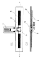
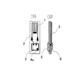
図1は、本発明の第1の実施形態であるひずみゲージの概略構成図である。図1の(a)は、ひずみゲージの平面を示し、図1の(b)は、図1の(a)におけるA−A’線に沿った断面を示す。
Hereinafter, embodiments of the present invention will be described in detail with reference to the accompanying drawings.
FIG. 1 is a schematic configuration diagram of a strain gauge according to the first embodiment of the present invention. 1A shows a plane of the strain gauge, and FIG. 1B shows a cross section along the line AA ′ in FIG.
図1において、被測定対象物に貼り付け、あるいは埋め込まれるひずみ感応ゲージ部1は、Ni−Cr系合金やCuNi合金等によるひずみ感応抵抗体がテープ基材2の表面に添着形成されて構成されている。ひずみゲージの種類については、測定対象や目的によって異なるため、ひずみ一般を測定するものからクラック進展を測定するものまで本発明は適用可能である。
In FIG. 1, a strain sensitive gauge portion 1 that is attached to or embedded in a measurement object is configured by a strain sensitive resistor made of Ni—Cr alloy or CuNi alloy attached to the surface of a
ゲージ部1から引き出された配線は、同一のテープ基材2に実装されている無線機能付きチップ3に接続されている。さらに、無線機能付きチップ(無線送信部又は無線送受信部)3が搭載されている同一のテープ基材2上にはアンテナ回路として金属性の箔4が形成されている。
The wiring drawn out from the gauge unit 1 is connected to the
アンテナ回路としての箔4は金属性のバンプ5を介して無線機能付きチップ3に接続されている。そして、無線機能付チップ3は、樹脂6により覆われ保護されている。
The
無線機能付きチップ3には、各ひずみゲージ固有のID番号を読み取り可能な形式で保存可能なROM機能を始めとして、ブリッジ抵抗回路、増幅機能回路、A/D変換機能回路、自己発電機能回路、無線送受信機能回路(RF回路)、及びそれら全体を制御するロジック回路を有している。そして、この無線機能付チップ3と外部との情報のやり取りを無線形式で行うことができる。
The chip with
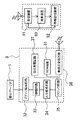
図2は、無線機能付チップ3と、この無線機能付チップ3と無線信号を送受信する送受信手段の概略機能ブロック図である。
FIG. 2 is a schematic functional block diagram of the wireless function-equipped
図2において、無線機能付チップ3は、ブリッジ抵抗回路32と、増幅回路33と、A/D変換回路34と、ロジック回路35と、無線送受信機能回路(RF回路)36と、自己発電回路37と、ROM機能回路31とを備えている。
In FIG. 2, the
ひずみ感応ゲージ部1の抵抗変動が電圧変動として、出力ブリッジ抵抗回路32を介して増幅回路33に供給される。そして、増幅回路33に供給された電圧変動が、この増幅回路33で増幅され、A/D変換回路34において、増幅されたアナログ電圧値がデジタル値に変換される。
The resistance fluctuation of the strain sensitive gauge unit 1 is supplied to the
また、自己発電回路37を有することで、外部からの電力供給がなくても駆動電力を自ら供給することができる。自己発電回路37としては、例えば微小振動を利用した発電回路構造があり、高速道路の橋脚等では絶えず振動が発生しているため機能するのに十分な電力供給が可能となる。
In addition, by having the self-
またROM機能回路31を有することで、各ひずみゲージに固有のIDを定義することができるので、大量の計測点数に対しても、測定結果がどの位置の出力結果かを簡便に特定することが可能となる。
In addition, since the
ロジック回路35は、自己発電回路37から供給される電力で動作し、A/D変換回路34から供給されたデジタル値に、ROM機能回路31に格納されたID情報等を付加し、無線送受信回路36を介して、無線信号を発信する。
The
無線機能付チップ3から発信された無線信号は、受信装置91に受信され、演算装置93により、ひずみゲージが貼付された構造体の変形状態が演算される。そして、演算装置93により演算されたデータが情報記憶装置92に格納される。
The wireless signal transmitted from the
なお、ロジック回路35には、内部記憶回路が備えられており、情報送信装置(図示省略)からの指令(計測間隔、情報送信間隔等)が無線送受信回路36を介して供給され、記憶される。
The
なお、無線機能付チップ3は、図2に示した機能要素を必ずしもすべて備えている必要は無く、ひずみ量の測定、情報の処理、外部との情報の送受信という一連の作業を、外部との配線を必要とせずに行うことができる機能を満足しているのであれば、上述した機能のうち、削除もしくは変更する要素があってもよい。
Note that the
例えば、ブリッジ抵抗回路32については、特許文献1に示されているように、ひずみ感応ゲージ部に一対のアクティブゲージと一対のダミーゲージとを一体で添着した構成とすれば、温度補償の問題が解決されると同時に別途にブリッジ抵抗回路を形成する必要もなくなる。
For example, with respect to the
また、無線アンテナ4をアンテナコイルにして、外部からの電磁波によって誘発される電磁誘導により駆動電力を発生させる構成とすることも可能である。この場合には、構造体の振動等により発電する自己発電機能は必要ではなくなる。
Moreover, it is also possible to employ a configuration in which the driving power is generated by electromagnetic induction induced by an external electromagnetic wave using the
次に、図1に示した無線機能付チップ3を搭載するひずみゲージの構造について説明する。
図1の(b)に断面で示すように、無線機能付きチップ3の電極部には金属製のバンプ5が形成され、テープ基材2上のデバイスホールに形成された箔状のリード線と接合される。
Next, the structure of the strain gauge on which the
As shown in a cross section in FIG. 1 (b),
通常、チップ3上に形成される金属製のバンプ5としては金バンプが用いられ、表面が金メッキされたリード配線とは、300℃以上に加熱された熱圧着ツールによる、金/金の金属接合によって接続される。
Usually, gold bumps are used as the metal bumps 5 formed on the
さらに、チップ3の回路面側を外部環境から長期にわたって保護する目的で、エポキシ系の樹脂6で封止、固定される。
Further, the
また、本発明の第1の実施形態においては、ひずみ感応ゲージ部1の位置と、アンテナ4の形状との関係から、T字型のテープ基板構成で示されているが、この構成についても、製造プロセス上の都合や用途によって、T字型に限ること無く、構造変更されてもよい。
Further, in the first embodiment of the present invention, from the relationship between the position of the strain sensitive gauge portion 1 and the shape of the
以上のように、本発明の第1の実施形態によれば、ひずみ感応ゲージ部1と、無線送受信アンテナ4と、ひずみ感応ゲージ部1により検出された対象物のひずみ値を、無線送受信アンテナ4を介して、無線発信するための発信駆動回路であるチップ3とを備えているので、大型構造物、建築物の変形状態や高速回転構造体の回転中の変形状態を、煩雑な配線処理を施すことなく、正確に実行可能なひずみゲージを実現することができる。
As described above, according to the first embodiment of the present invention, the strain value of the object detected by the strain-sensitive gauge unit 1, the wireless transmission /
本発明の一実施形態による無線機能付チップを搭載したひずみゲージを、橋梁等の大型構造物に複数箇所備え付け、複数の箇所から構造体の変形情報を入手することができれば、車両等の走行による振動時の変形量と変形箇所、振動が生じていないときにおける変形量と変形箇所とを比較して、解析することにより、構造体の安全性の確認や、強度の低下予測等を行うことも可能となる。 If a strain gauge equipped with a chip with a wireless function according to an embodiment of the present invention is provided in a plurality of locations on a large structure such as a bridge, and deformation information of the structure can be obtained from the plurality of locations, it is possible to By comparing and analyzing the deformation amount and the deformation location during vibration, and the deformation amount and deformation location when vibration is not occurring, it is also possible to confirm the safety of the structure, predict strength reduction, etc. It becomes possible.
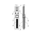
図3は、本発明の第2の実施形態であるひずみゲージの概略構成図である。図3の(a)は、ひずみゲージの平面を示し、図3の(b)は、図3の(a)におけるA−A’線に沿った断面を示す。 FIG. 3 is a schematic configuration diagram of a strain gauge according to the second embodiment of the present invention. 3A shows a plane of the strain gauge, and FIG. 3B shows a cross section taken along the line A-A ′ in FIG.
この第2の実施形態における基本構成は、第1の実施形態と同様であるが、無線機能付きチップ3は金属バンプ5を有し、この金属バンプ5とリード配線とは、テープ基材2上に形成された配線パターン上に、接着剤6a(異方導電性、非導電性)を介して180〜200℃での熱圧着(超音波加振があってもよい)により接続される。
The basic configuration of the second embodiment is the same as that of the first embodiment, but the
上述した第1の実施形態では、金属バンプ5とリード配線との接続については、金/金の金属結合を達成するため、接合部付近を300℃以上に加熱する必要があり、チップ3上に形成された回路機能がこの程度の加熱によって影響されることはないが、温度に対して影響を受けやすい、ひずみ感応ゲージ部1が隣接して存在するため、できるだけ低温プロセスで組立てを実施できるのが望ましい。
In the first embodiment described above, for the connection between the
このため、第2の実施形態においては、接着剤6aを介して、180〜200℃で熱圧着による接着を行っている。
For this reason, in 2nd Embodiment, the adhesion | attachment by thermocompression bonding is performed at 180-200 degreeC via the
また、基材2上に形成された配線パターン上に直接チップ3を搭載することが可能であるため、デバイスホール等の余分なスペースを必要とせず小型化に適している。
In addition, since the
以上、本発明の第2の実施形態によれば、第1の実施形態と同様な効果を得ることができる他、低温プロセスで組み立てを実行して、ひずみ感応ゲージ部1の熱影響を抑制できる。また、小型化を実現できるという効果がある。 As described above, according to the second embodiment of the present invention, it is possible to obtain the same effect as that of the first embodiment, and it is possible to suppress the thermal influence of the strain sensitive gauge unit 1 by performing assembly in a low temperature process. . In addition, there is an effect that downsizing can be realized.
図4は、本発明の第3の実施形態であるひずみゲージの概略構成図である。
上述した第1及び第2の実施形態においては、ひずみゲージの抵抗変化量を、電圧変換して増幅し、それをデジタル信号に変換し、変換した信号を無線によって受信機側へと送信する機能をすべて1チップに集積した無線機能付きチップが搭載されている。
FIG. 4 is a schematic configuration diagram of a strain gauge according to the third embodiment of the present invention.
In the first and second embodiments described above, the resistance change amount of the strain gauge is amplified by voltage conversion, converted into a digital signal, and the converted signal is transmitted to the receiver side by radio. A chip with a wireless function in which all of these are integrated in one chip is mounted.
理論的には、これらの機能を1チップに集積することも可能であるが、多様な機能を1チップに集積する場合、一般に開発期間を要し、かつ、歩留りも低くなるため製造コストが高くなるという問題がある。 Theoretically, these functions can be integrated on a single chip. However, when various functions are integrated on a single chip, generally a development period is required and the yield is low, resulting in high manufacturing costs. There is a problem of becoming.
そこで、図4に示す第3の実施形態においては、電圧変換増幅機能、アナログーデジタル変換機能、信号無線送信機能のそれぞれの機能を、それぞれ特定化した複数の回路構成とすることで、低コストの複数チップ(電圧変換増幅チップ3a、アナログーデジタル変換チップ3b、信号無線送信チップ3c)としている。
Therefore, in the third embodiment shown in FIG. 4, the voltage conversion amplification function, the analog-digital conversion function, and the signal wireless transmission function are configured with a plurality of specific circuit configurations, thereby reducing the cost. A plurality of chips (voltage
この第3の実施形態の場合、各チップ3a〜3c間の配線パターンは、ひずみ感応ゲージ部1と一体化したテープ基材2上に同時形成される。
In the case of the third embodiment, the wiring pattern between the
したがって、第3の実施形態によれば、第2の実施形態と同等な効果を得ることができる他、第2の実施形態と比較して、ひずみ感応ゲージ部1を搭載したテープ基材のコストを上げることなく、かつ低コストのチップ3a〜3cを用いて同等機能を達成することが可能となる。
Therefore, according to the third embodiment, an effect equivalent to that of the second embodiment can be obtained, and the cost of the tape base material on which the strain sensitive gauge unit 1 is mounted as compared with the second embodiment. It is possible to achieve an equivalent function using low-
図5は、本発明の第4の実施形態であるひずみゲージの概略構成図である。
上述した、第3の実施形態のように、複数のチップ3a〜3cを二次元配置で実装すると、ひずみ感応ゲージ部1のエリアに比べて非常に大きな占有スペースを必要とする。
FIG. 5 is a schematic configuration diagram of a strain gauge according to the fourth embodiment of the present invention.
When the plurality of
そこで、複数のチップの一部(ここでは、チップ3aと3c)を三次元的に積層実装することで、実装スペースの大幅な縮小が可能となる。
Therefore, a part of the plurality of chips (here,
この場合、下段側のチップ3aは第2の実施形態のように、チップ電極部とテープ基材2上の配線パターン間を、接着剤6aを介した熱圧着により接続され、上段のチップ3cはワイヤボンディングにより電気的に接合される。そして、最後に全体がエポキシ系の樹脂5で封止される。
In this case, as in the second embodiment, the
本発明の第4の実施形態によれば、第3の実施形態と同様な効果を得ることができる他、第3の実施形態と比較して、実装スペースの大幅な縮小が可能となる。 According to the fourth embodiment of the present invention, the same effect as that of the third embodiment can be obtained, and the mounting space can be significantly reduced as compared with the third embodiment.
図6は、本発明の第5の実施形態であるひずみゲージの概略構成図であり、図6の(a)は平面、図6の(b)は断面を示している。この第6の実施形態は、上述した第1〜第4の実施形態におけるアンテナ配置を変更した例である。 6A and 6B are schematic configuration diagrams of a strain gauge according to a fifth embodiment of the present invention, in which FIG. 6A shows a plan view and FIG. 6B shows a cross section. The sixth embodiment is an example in which the antenna arrangement in the first to fourth embodiments described above is changed.
半導体チップを搭載したひずみゲージを製造する場合、ひずみ感応ゲージ部1と半導体チップ搭載部の配線、配線パターン、及びアンテナ配線が一体形成されたテープ状のフレキシブル基板2がリールに巻きつけられた状態で入荷される。そして、TAB(Tape Automated Bonding)方式によって半導体チップを実装・組立てるプロセスが最も一般的である。
When manufacturing a strain gauge mounted with a semiconductor chip, a tape-like
したがって、第1から第4の実施形態のように最終製品形態が、T字型の構造では、最終切断工程でテープ基材を有効に使用することが困難となる場合もあり、材料コストの観点からは改善の余地がある。 Therefore, when the final product form is a T-shaped structure as in the first to fourth embodiments, it may be difficult to effectively use the tape base material in the final cutting step, which is a viewpoint of material cost. There is room for improvement.
そこで、図6に示すように、アンテナ配線4をひずみ感応ゲージ部1と平行にテープ基材2の両面に形成した構造にすることによって、リール状のフレキシブル基板を無駄に切り捨てる必要も無く、小型でかつ梱包性にも優れた構造とすることができる。
Therefore, as shown in FIG. 6, the
したがって、本発明の第5の実施形態によれば、第1の実施形態と同様な効果を得るこができる他、小型で、かつ梱包性にも優れた構造とすることができる。 Therefore, according to the fifth embodiment of the present invention, the same effect as that of the first embodiment can be obtained, and the structure can be made small and excellent in packing property.
図7は、本発明の第6の実施形態であるひずみゲージの概略構成図であり、図7の(a)は平面、図7の(b)は断面を示している。この第6の実施形態はアンテナ回路4aをチップに内蔵した実施例である。
7A and 7B are schematic configuration diagrams of a strain gauge according to a sixth embodiment of the present invention. FIG. 7A shows a plan view, and FIG. 7B shows a cross section. The sixth embodiment is an example in which an
第1から第5の実施例においては、金属製の箔で形成されたアンテナパターン4をテープ基材2上に形成した構造であるが、この第6の実施形態においては、無線機能付きチップ3上に微小なアンテナ回路4aが形成されている。
In the first to fifth embodiments, the
これにより、これまでアンテナパターンに要していたスペースが不要となり大幅な小型化が達成可能となる。 This eliminates the need for the space required for the antenna pattern so far, and enables a significant reduction in size.
図8は、本発明の第7の実施形態を示す図である。この第7の実施形態は、第1から第6の実施形態による無線機能付きチップ1を搭載したひずみゲージの具体的な適用事例に基づく例である。 FIG. 8 is a diagram showing a seventh embodiment of the present invention. The seventh embodiment is an example based on a specific application example of the strain gauge on which the wireless function chip 1 according to the first to sixth embodiments is mounted.
高速道路の橋脚構造は、短柱橋脚7(図8の(a))やラーメン橋脚構造8(図8の(b))が主に適用されている。現状の橋脚設計においては、想定される振動や過負荷に対して寿命設計がなされている。しかし、実際には想定外の交通量の増加や、路線による通行量の変動によって、橋脚の劣化状態はさまざまである。このため、その劣化状態の把握には、すべての橋脚に対して専門技術者の目視による検査等を実施しなければならない。 As the pier structure of the expressway, the short column pier 7 (FIG. 8A) and the ramen pier structure 8 (FIG. 8B) are mainly applied. In the current pier design, the life is designed against the expected vibration and overload. In reality, however, the deterioration of the piers varies depending on unexpected increases in traffic and fluctuations in traffic. For this reason, in order to grasp the deterioration state, it is necessary to carry out a visual inspection by a specialist engineer on all piers.
そこで、長期間にわたる使用によって、橋脚のどの部分に劣化又は欠陥が進行するかを事前に詳細検討し、劣化・欠陥診断を実施するのに適正なゲージ貼り付け位置(あるいはゲージ埋め込み位置)を特定する。 Therefore, we will examine in advance in advance which part of the pier will deteriorate or become defective over a long period of use, and identify the appropriate gauge attachment position (or gauge embedding position) for conducting deterioration and defect diagnosis. To do.
この作業は、通常専門家による構造シミュレーション解析等により初期設計段階において検討され、橋脚設計に反映される。ここで示したような橋脚構造においては、自動車の通行に伴う負荷振動によって、図8の丸囲みで示した橋脚隅角部11に応力集中が生じて亀裂が発生することがわかっている。
This work is usually examined at the initial design stage by structural simulation analysis by experts and reflected in the pier design. In the pier structure as shown here, it is known that stress concentration occurs in the
この例においては、橋脚の施工段階で事前に隅角部11の数箇所に、第1から第6の実施形態のうちのいずれかの無線機能付きチップを搭載したひずみゲージを貼付又は埋め込む。
In this example, strain gauges equipped with the wireless function chip of any one of the first to sixth embodiments are pasted or embedded in several locations of the
貼付又は埋め込まれた無線ひずみゲージから送信される橋脚変形情報(ひずみ測定データ、測定箇所、測定時間)が送受信装置9により受信され、自動的に記録される。記録されたデータを解析することにより、橋脚の亀裂が最も発生しやすい隅角部の負荷・変形状態について簡便に把握することが可能になる。 The pier deformation information (strain measurement data, measurement location, measurement time) transmitted from the affixed or embedded wireless strain gauge is received by the transmission / reception device 9 and automatically recorded. By analyzing the recorded data, it is possible to easily grasp the load / deformation state of the corner where the pier crack is most likely to occur.
これにより、膨大な人件費を要する目視による定期点検は大幅な簡略化ができるようになり、かつ膨大な数の橋脚に対して、劣化状態がある程度まで把握できるようになる。 This makes it possible to greatly simplify visual inspections that require a large amount of labor costs, and to grasp the deterioration state to some extent for a huge number of piers.
したがって、橋脚等の大規模構造物に対して、計画的なメンテナンスを実施できるようになり安全管理の観点からも非常に有効なシステムとなる。 Therefore, planned maintenance can be performed on large-scale structures such as bridge piers, and the system is very effective from the viewpoint of safety management.
なお、本発明は、橋脚以外の大規模構造物や、回転体の変形測定に適用可能である。例えば、原子力機器の配管系の安全管理や、航空機の安全管理等への適用も有効であると考えられ、適用範囲については制限されるものではない。 In addition, this invention is applicable to the deformation | transformation measurement of large-scale structures other than a bridge pier, and a rotary body. For example, it is considered that application to safety management of nuclear equipment piping systems and aircraft safety management is also effective, and the scope of application is not limited.
また、上述した例においては、チップ3は、送受信機能を備えているが、受信機能はなく、送信機能のみ備えていてもよい。
In the example described above, the
また、ひずみゲージからの測定対象物変形情報は、常時、発信するように構成することも可能であるが、省電力化の観点から、一定周期で、発信してもよいし、定時刻に発信するように構成してもよい。 In addition, the deformation information of the measurement object from the strain gauge can be configured to be transmitted at all times. However, from the viewpoint of power saving, it may be transmitted at regular intervals or at a fixed time. You may comprise.
1 ひずみ感応ゲージ部
2 テープ基材
3 無線機能付き半導体チップ
3a〜3c チップ
4 アンテナパターン
4a アンテナ回路
5 金属製バンプ
6 封止樹脂
6a 接着剤(異方導電、非導電性)
7 短柱橋脚
8 ラーメン橋脚
9 送受信装置
31 ROM機能回路
32 ブリッジ抵抗回路
33 増幅回路
34 A/D変換回路
35 ロジック回路
36 無線送受信回路(RF回路)
37 自己発電回路
91 受信装置
92 記録装置(媒体)
93 演算装置
DESCRIPTION OF SYMBOLS 1 Strain-
7 Short pillar pier 8 Ramen pier 9 Transmitter /
37 Self-generating
93 Arithmetic unit
Claims (8)
上記ひずみ感応ゲージ部により測定された測定対象物のひずみ情報を、無線発信するための無線送信部と、
上記無線送信部からの信号を無線発信するアンテナ部と、
を備え、上記ひずみ感応ゲージ部、無線送信部及びアンテナ部は、配線パターンが形成されたテープ基材上に配置されていることを特徴とするひずみゲージ。 A strain-sensitive gauge section that measures the strain of the measurement object by changing the conductor resistance accompanying the deformation of the measurement object;
A wireless transmission unit for wirelessly transmitting strain information of the measurement object measured by the strain sensitive gauge unit;
An antenna unit that wirelessly transmits a signal from the wireless transmission unit;
The strain-sensitive gauge part, the wireless transmission part, and the antenna part are arranged on a tape base material on which a wiring pattern is formed.
Priority Applications (1)
| Application Number | Priority Date | Filing Date | Title |
|---|---|---|---|
| JP2004109167A JP2005291999A (en) | 2004-04-01 | 2004-04-01 | Strain gauge equipped with a chip with wireless function |
Applications Claiming Priority (1)
| Application Number | Priority Date | Filing Date | Title |
|---|---|---|---|
| JP2004109167A JP2005291999A (en) | 2004-04-01 | 2004-04-01 | Strain gauge equipped with a chip with wireless function |
Publications (1)
| Publication Number | Publication Date |
|---|---|
| JP2005291999A true JP2005291999A (en) | 2005-10-20 |
Family
ID=35325082
Family Applications (1)
| Application Number | Title | Priority Date | Filing Date |
|---|---|---|---|
| JP2004109167A Pending JP2005291999A (en) | 2004-04-01 | 2004-04-01 | Strain gauge equipped with a chip with wireless function |
Country Status (1)
| Country | Link |
|---|---|
| JP (1) | JP2005291999A (en) |
Cited By (11)
| Publication number | Priority date | Publication date | Assignee | Title |
|---|---|---|---|---|
| JP2007327172A (en) * | 2006-06-06 | 2007-12-20 | Fujita Corp | Data collection system for shield method and segment attachment status |
| JP2011179817A (en) * | 2010-02-26 | 2011-09-15 | Taiheiyo Cement Corp | Strain measuring device and strain measuring system |
| JP2017016658A (en) * | 2015-07-06 | 2017-01-19 | ゼネラル・エレクトリック・カンパニイ | Passive wireless sensors for rotary machines |
| JP2017062139A (en) * | 2015-09-24 | 2017-03-30 | Ntn株式会社 | Multiple simultaneous states determining system for machine components |
| JP2020536752A (en) * | 2017-10-04 | 2020-12-17 | サンーゴバン アブレイシブズ,インコーポレイティド | Polishing article and its forming method |
| CN116295235A (en) * | 2023-04-10 | 2023-06-23 | 中交四航局第一工程有限公司 | A Deformation Monitoring Method of Composite Support Structure |
| US11787494B2 (en) | 2020-04-23 | 2023-10-17 | Shimano Inc. | Component for human-powered vehicle |
| US12005985B2 (en) | 2020-04-23 | 2024-06-11 | Shimano Inc. | Component for human-powered vehicle |
| JP2024155293A (en) * | 2023-04-21 | 2024-10-31 | 株式会社栗本鐵工所 | Method for monitoring the condition of a resin inspection path and a resin inspection path |
| US12226876B2 (en) | 2019-04-03 | 2025-02-18 | Saint-Gobain Abrasives, Inc. | Abrasive article, abrasive system and method for using and forming same |
| US12330265B2 (en) | 2019-03-29 | 2025-06-17 | Saint-Gobain Abrasives, Inc. | Performance grinding solutions |
-
2004
- 2004-04-01 JP JP2004109167A patent/JP2005291999A/en active Pending
Cited By (15)
| Publication number | Priority date | Publication date | Assignee | Title |
|---|---|---|---|---|
| JP2007327172A (en) * | 2006-06-06 | 2007-12-20 | Fujita Corp | Data collection system for shield method and segment attachment status |
| JP2011179817A (en) * | 2010-02-26 | 2011-09-15 | Taiheiyo Cement Corp | Strain measuring device and strain measuring system |
| JP2017016658A (en) * | 2015-07-06 | 2017-01-19 | ゼネラル・エレクトリック・カンパニイ | Passive wireless sensors for rotary machines |
| US10005551B2 (en) | 2015-07-06 | 2018-06-26 | General Electric Company | Passive wireless sensors for rotary machines |
| JP2017062139A (en) * | 2015-09-24 | 2017-03-30 | Ntn株式会社 | Multiple simultaneous states determining system for machine components |
| JP7186770B2 (en) | 2017-10-04 | 2022-12-09 | サンーゴバン アブレイシブズ,インコーポレイティド | Abrasive article and method of forming same |
| JP2020536752A (en) * | 2017-10-04 | 2020-12-17 | サンーゴバン アブレイシブズ,インコーポレイティド | Polishing article and its forming method |
| JP2023022202A (en) * | 2017-10-04 | 2023-02-14 | サンーゴバン アブレイシブズ,インコーポレイティド | Abrasive article and method for forming the same |
| US11712784B2 (en) | 2017-10-04 | 2023-08-01 | Saint-Gobain Abrasives, Inc. | Abrasive article and method for forming same |
| US12330265B2 (en) | 2019-03-29 | 2025-06-17 | Saint-Gobain Abrasives, Inc. | Performance grinding solutions |
| US12226876B2 (en) | 2019-04-03 | 2025-02-18 | Saint-Gobain Abrasives, Inc. | Abrasive article, abrasive system and method for using and forming same |
| US11787494B2 (en) | 2020-04-23 | 2023-10-17 | Shimano Inc. | Component for human-powered vehicle |
| US12005985B2 (en) | 2020-04-23 | 2024-06-11 | Shimano Inc. | Component for human-powered vehicle |
| CN116295235A (en) * | 2023-04-10 | 2023-06-23 | 中交四航局第一工程有限公司 | A Deformation Monitoring Method of Composite Support Structure |
| JP2024155293A (en) * | 2023-04-21 | 2024-10-31 | 株式会社栗本鐵工所 | Method for monitoring the condition of a resin inspection path and a resin inspection path |
Similar Documents
| Publication | Publication Date | Title |
|---|---|---|
| JP2005291999A (en) | Strain gauge equipped with a chip with wireless function | |
| JP2010053927A (en) | Fastening apparatus and system for detecting axial force thereof | |
| US8151643B2 (en) | Device for non-destructive testing of a structure by vibratory analysis | |
| EP2035771B1 (en) | Displacement, strain and force sensor | |
| CN105089718B (en) | Embedded type wireless sensing device for turbine components defect inspection | |
| US9726587B2 (en) | Tensile stress measurement device with attachment plates and related methods | |
| CN205209660U (en) | Pressure sensing equipment | |
| JP6267601B2 (en) | Passive crack sensor | |
| JP5779662B2 (en) | Mechanical quantity measuring device | |
| US20100005895A1 (en) | Smart coat for damage detection information, detecting device and damage detecting method using said coating | |
| JPH0886707A (en) | Stress compounding sensor and stress measuring device of structural body by using this | |
| JP7132009B2 (en) | Mounting structure of wireless communication module, installation method of wireless communication module, and state quantity measurement system | |
| CN106909733A (en) | Health state monitoring method for high-strength bolt of key component of steel truss bridge | |
| JP2002221453A (en) | System for collecting load information of structure | |
| CN102759720B (en) | Magnetic sensor easy to encapsulate | |
| GB2591461A (en) | Apparatus and method for the detection of properties of a pipe | |
| CN101858888B (en) | Structure damage positioning device based on metal core bearing piezoelectric fiber | |
| CN113552220B (en) | Reinforced concrete structure health monitoring system | |
| US9506823B2 (en) | Bonding stress testing arrangement and method of determining stress | |
| Obadat et al. | Full-scale field evaluation of microelectromechanical system-based biaxial strain transducer and its application in fatigue analysis | |
| Gromala et al. | Prognostic approaches for the wirebond failure prediction in power semiconductors: A case study using DPAK package | |
| JP2006313800A (en) | Method for predicting connection reliability of mounting structure in semiconductor device and semiconductor device | |
| JP2008145403A (en) | Strain measuring system and IC tag | |
| CN110207860B (en) | Monitoring device for normal/shear stress of bonding interface of solid rocket engine | |
| CN113065624A (en) | Non-destructive testing system and method for fatigue cracks of orthotropic steel bridge deck slab |
Legal Events
| Date | Code | Title | Description |
|---|---|---|---|
| A621 | Written request for application examination |
Free format text: JAPANESE INTERMEDIATE CODE: A621 Effective date: 20060606 |
|
| A131 | Notification of reasons for refusal |
Free format text: JAPANESE INTERMEDIATE CODE: A131 Effective date: 20081014 |
|
| A521 | Written amendment |
Free format text: JAPANESE INTERMEDIATE CODE: A523 Effective date: 20081215 |
|
| A02 | Decision of refusal |
Free format text: JAPANESE INTERMEDIATE CODE: A02 Effective date: 20090609 |