JP2005252281A5 - - Google Patents
Download PDFInfo
- Publication number
- JP2005252281A5 JP2005252281A5 JP2005099664A JP2005099664A JP2005252281A5 JP 2005252281 A5 JP2005252281 A5 JP 2005252281A5 JP 2005099664 A JP2005099664 A JP 2005099664A JP 2005099664 A JP2005099664 A JP 2005099664A JP 2005252281 A5 JP2005252281 A5 JP 2005252281A5
- Authority
- JP
- Japan
- Legal status (The legal status is an assumption and is not a legal conclusion. Google has not performed a legal analysis and makes no representation as to the accuracy of the status listed.)
- Granted
Links
Images


Applications Claiming Priority (2)
| Application Number | Priority Date | Filing Date | Title |
|---|---|---|---|
| US10/790,252 US20050195378A1 (en) | 2004-03-02 | 2004-03-02 | Lithographic apparatus, method of substrate identification, device manufacturing method, substrate, and computer program |
| US10/954,654 US7177009B2 (en) | 2004-10-01 | 2004-10-01 | Position determination method and lithographic apparatus |
Publications (3)
| Publication Number | Publication Date |
|---|---|
| JP2005252281A JP2005252281A (en) | 2005-09-15 |
| JP2005252281A5 true JP2005252281A5 (en) | 2005-10-27 |
| JP4340638B2 JP4340638B2 (en) | 2009-10-07 |
Family
ID=35032411
Family Applications (1)
| Application Number | Title | Priority Date | Filing Date |
|---|---|---|---|
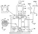
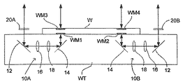
| JP2005099664A Expired - Fee Related JP4340638B2 (en) | 2004-03-02 | 2005-03-02 | Lithographic apparatus, substrate identification method, device manufacturing method, substrate, and computer program for imaging on the front or back side of the substrate |
Country Status (2)
| Country | Link |
|---|---|
| US (1) | US7480028B2 (en) |
| JP (1) | JP4340638B2 (en) |
Families Citing this family (10)
| Publication number | Priority date | Publication date | Assignee | Title |
|---|---|---|---|---|
| US20050118532A1 (en) * | 2003-11-14 | 2005-06-02 | International Business Machines Corporation | Back to Front Alignment with Latent Imaging |
| EP1744217B1 (en) * | 2005-07-12 | 2012-03-14 | ASML Netherlands B.V. | Method of selecting a grid model for correcting grid deformations in a lithographic apparatus and lithographic assembly using the same |
| US20080020303A1 (en) * | 2006-07-24 | 2008-01-24 | Wei Wu | Alignment for contact lithography |
| US7808613B2 (en) * | 2006-08-03 | 2010-10-05 | Asml Netherlands B.V. | Individual wafer history storage for overlay corrections |
| JP5064079B2 (en) * | 2007-03-30 | 2012-10-31 | 富士フイルム株式会社 | Drawing method and drawing system |
| DE102009019140B4 (en) * | 2009-04-29 | 2017-03-02 | Carl Zeiss Smt Gmbh | Method for calibrating a position measuring device and method for measuring a mask |
| US10976572B2 (en) | 2011-12-22 | 2021-04-13 | Carl Zeiss Vision International Gmbh | Method for storing information on a spectacles lens, spectacles lens blank or spectacles lens semi-finished product |
| JP6945316B2 (en) * | 2017-03-24 | 2021-10-06 | キヤノン株式会社 | Detection device, pattern forming device, acquisition method, detection method, and article manufacturing method |
| CN114908329B (en) * | 2021-02-08 | 2024-03-08 | 台湾积体电路制造股份有限公司 | Correction method and semiconductor manufacturing apparatus |
| CN117457550B (en) * | 2023-12-26 | 2024-03-29 | 深圳市森美协尔科技有限公司 | Wafer alignment method and related device |
Family Cites Families (12)
| Publication number | Priority date | Publication date | Assignee | Title |
|---|---|---|---|---|
| JPH0443358A (en) * | 1990-06-11 | 1992-02-13 | Fujitsu Ltd | Method for forming chip position identifying pattern |
| JP2789818B2 (en) * | 1990-12-27 | 1998-08-27 | 富士電機株式会社 | Semiconductor wafer identification method |
| JPH05217843A (en) * | 1992-01-27 | 1993-08-27 | Nec Corp | Stepper |
| JP3637680B2 (en) * | 1996-04-02 | 2005-04-13 | 株式会社ニコン | Exposure equipment |
| US6710847B1 (en) * | 1998-11-06 | 2004-03-23 | Nikon Corporation | Exposure method and exposure apparatus |
| US6768539B2 (en) * | 2001-01-15 | 2004-07-27 | Asml Netherlands B.V. | Lithographic apparatus |
| EP1353229A1 (en) * | 2002-04-09 | 2003-10-15 | ASML Netherlands B.V. | Lithographic apparatus, device manufacturing method and device manufactured thereby |
| JP2004006527A (en) * | 2002-05-31 | 2004-01-08 | Canon Inc | Position detection device and position detection method, exposure device, and device manufacturing method and substrate |
| KR100549781B1 (en) * | 2002-12-19 | 2006-02-06 | 에이에스엠엘 네델란즈 비.브이. | A Lithographic Projection Mask, a Device Manufacturing Method Using a Lithographic Projection Mask and a Device Manufactured Thereby |
| JP3913715B2 (en) * | 2003-06-18 | 2007-05-09 | 株式会社東芝 | Defect detection method |
| US7177009B2 (en) * | 2004-10-01 | 2007-02-13 | Asml Netherlands B.V. | Position determination method and lithographic apparatus |
| US7259828B2 (en) * | 2004-05-14 | 2007-08-21 | Asml Netherlands B.V. | Alignment system and method and device manufactured thereby |
-
2005
- 2005-03-02 JP JP2005099664A patent/JP4340638B2/en not_active Expired - Fee Related
- 2005-03-02 US US11/069,058 patent/US7480028B2/en not_active Expired - Lifetime
Similar Documents
| Publication | Publication Date | Title |
|---|---|---|
| BRPI0601358B8 (pt) | Aplicador de clipe cirúrgico | |
| BRPI0601402B8 (pt) | Aplicador de grampos cirúrgicos | |
| BR122017004707A2 (en) | ||
| BRPI0609157A8 (en) | ||
| BRPI0608519A2 (en) | ||
| BR122020005056A2 (en) | ||
| JP2005322908A5 (en) | ||
| BRPI0604219A (en) | ||
| JP2005252281A5 (en) | ||
| BRPI0618215B8 (en) | ||
| JP2006212777A5 (en) | ||
| JP2005153141A5 (en) | ||
| JP2006276485A5 (en) | ||
| BY2237U (en) | ||
| JP2006227909A5 (en) | ||
| CN105122969C (en) | ||
| CN300726698S (zh) | 调料瓶套装(e) | |
| CN300726591S (zh) | 冷冰食品制作器 | |
| CN300726699S (zh) | 调料瓶套装(d) | |
| CN300726006S (zh) | 鞋底 | |
| CN300726007S (zh) | 鞋底 | |
| CN300726008S (zh) | 鞋帮 | |
| CN300726015S (zh) | 鞋底 | |
| CN300726016S (zh) | 鞋帮 | |
| CN300726001S (zh) | 鞋帮 |