JP2005235777A - Inspection apparatus and method by electron beam, and device manufacturing method using the inspection apparatus - Google Patents
Inspection apparatus and method by electron beam, and device manufacturing method using the inspection apparatus Download PDFInfo
- Publication number
- JP2005235777A JP2005235777A JP2005061093A JP2005061093A JP2005235777A JP 2005235777 A JP2005235777 A JP 2005235777A JP 2005061093 A JP2005061093 A JP 2005061093A JP 2005061093 A JP2005061093 A JP 2005061093A JP 2005235777 A JP2005235777 A JP 2005235777A
- Authority
- JP
- Japan
- Prior art keywords
- electron beam
- sample
- inspection apparatus
- image
- electron
- Prior art date
- Legal status (The legal status is an assumption and is not a legal conclusion. Google has not performed a legal analysis and makes no representation as to the accuracy of the status listed.)
- Pending
Links
Images


Abstract
Description
本発明は、電子ビームを用いてウェーハなどの検査対象の表面に形成されたパターンの欠陥等を検査する検査装置に関し、詳しくは、半導体製造工程におけるウェーハの欠陥を検出する場合のように、電子ビームを検査対象に照射してその表面の性状に応じて変化する二次電子量から画像データを形成し、その画像データに基づいて検査対象の表面に形成されたパターン等を高いスループットで検査する検査装置、検査方法、並びにそのような検査装置を用いて歩留まり良くデバイスを製造するデバイス製造方法に関する。 The present invention relates to an inspection apparatus for inspecting a defect or the like of a pattern formed on the surface of an inspection object such as a wafer by using an electron beam, and more specifically, in the case of detecting a defect of a wafer in a semiconductor manufacturing process. Image data is formed from the amount of secondary electrons that change according to the surface properties by irradiating the beam to the inspection object, and patterns and the like formed on the surface of the inspection object are inspected with high throughput based on the image data. The present invention relates to an inspection apparatus, an inspection method, and a device manufacturing method for manufacturing a device with high yield using such an inspection apparatus.
半導体プロセスにおいて、デザインルールは100nmの時代を迎えようとしており、また生産形態はDRAMに代表される少品種大量生産からSOC(Silicon on chip)のように多品種少量生産へ移行しつつある。それに伴い、製造工程数が増加し、各工程毎の歩留まり向上は必須となり、プロセス起因の欠陥検査が重要になってきている。従来より、半導体プロセスにおける各工程後にウェーハの欠陥検査が行われている。そして、半導体デバイスの高集積化、パターンの微細化に伴い、高分解能、高スループットの欠陥検査装置が要求されている。というのは、100nmデザインルールのウェーハ一基板の欠陥を調べるためには、100nm以下の分解能が必要だからである。また、半導体デバイスの高集積化による製造工程の増加により、検査量が増大するため、高スループットが要求されるからである。さらに、半導体デバイスの多層化が進むにつれて、層間の配線をつなぐビアのコンタクト不良(電気的欠陥)を検出する機能も、欠陥検査装置に要求されている。 In the semiconductor process, the design rule is about to reach the age of 100 nm, and the production form is shifting from small-quantity mass production represented by DRAM to high-variety small-quantity production such as SOC (Silicon on chip). Along with this, the number of manufacturing processes has increased, and it has become essential to improve the yield of each process, and defect inspection due to processes has become important. Conventionally, a wafer defect inspection is performed after each step in a semiconductor process. Along with higher integration of semiconductor devices and miniaturization of patterns, a defect inspection apparatus with high resolution and high throughput is required. This is because a resolution of 100 nm or less is required in order to investigate a defect of one wafer of a 100 nm design rule. In addition, the amount of inspection increases due to an increase in the number of manufacturing processes due to high integration of semiconductor devices, and thus high throughput is required. Further, as the number of semiconductor devices increases, the defect inspection apparatus is also required to have a function of detecting a contact failure (electrical defect) of a via that connects wirings between layers.
この種の欠陥検査装置としては、従来より、光方式の欠陥検査装置が使用されている。しかしならが、光方式の欠陥検査装置においては、その分解能は使用する光の波長の1/2が限界であり、実用化されている可視光の例では0.2μm程度である。このように、光方式の欠陥検査装置においては、分解能が要求に追いつかないという問題点があった。さらに、光方式の欠陥検査装置では、半導体ウェーハに生じた電気的な導通不良(オープン、ショート不良など)、すなわち、コンタクト不良検査をすることができなかった。 Conventionally, optical defect inspection apparatuses have been used as this type of defect inspection apparatus. However, in the optical defect inspection apparatus, the resolution is limited to 1/2 of the wavelength of the light to be used, and is about 0.2 μm in the case of visible light that has been put into practical use. As described above, the optical defect inspection apparatus has a problem that the resolution cannot keep up with the demand. Furthermore, in the optical defect inspection apparatus, it is impossible to inspect the electrical continuity failure (open, short failure, etc.) generated in the semiconductor wafer, that is, contact failure inspection.
そこで、最近、光方式の欠陥検査装置に代わって電子ビームを用いた欠陥検査装置が開発されてきている。
かかる電子ビーム方式欠陥検査装置では、通常、走査型電子ビーム方式(SEM方式)が実用化されており、その分解能は0.1μmと比較的に高くなっており、電気的欠陥(配線の断線、導通不良、ビアの導通不良等)も検査可能となっている。しかし、SEMを応用した欠陥検査装置では、ビーム電流量と検出器の応答速度に限界があり、そのために、欠陥検査に多くの時間を必要としていた。例えば、検査時間には8時間/枚(20cmウェーハ)も要し、検査時間は非常に長く、スループット(単位時間当たりの検査量)が光方式の欠陥検査装置などの他のプロセス装置に比べて低いという問題点がある。また、電子ビーム方式欠陥検査装置は、非常に高価であるという問題点もある。そのため、半導体製造の各工程の後に使用することは困難な状態にあり、現状では重要な工程の後、例えばエッチング、成膜(銅メッキを含む)、又はCMP(化学機械研磨)平坦化処理後等に使用されている。
Therefore, a defect inspection apparatus using an electron beam has recently been developed in place of the optical defect inspection apparatus.
In such an electron beam system defect inspection apparatus, a scanning electron beam system (SEM system) is generally put into practical use, and its resolution is relatively high at 0.1 μm, and electrical defects (disconnection of wiring, Insufficient conduction, via conduction failure, etc.) can also be inspected. However, in the defect inspection apparatus using SEM, there is a limit to the beam current amount and the response speed of the detector, which requires a lot of time for defect inspection. For example, the inspection time takes 8 hours / piece (20 cm wafer), the inspection time is very long, and the throughput (inspection amount per unit time) is higher than that of other process equipment such as optical defect inspection equipment. There is a problem that it is low. Also, the electron beam type defect inspection apparatus is very expensive. Therefore, it is in a difficult state to use after each process of semiconductor manufacturing. At present, after an important process, for example, after etching, film formation (including copper plating), or CMP (chemical mechanical polishing) planarization treatment Etc. are used.
このような走査型電子ビーム方式(SEM方式)を用いた欠陥検査装置を更に説明すると、かかる欠陥検査装置では、電子ビームを細く絞って(このビーム径が分解能に相当する)これを走査してライン状にウェーハなどの試料を照射する。一方、ウェーハを載置したステージを、電子ビームの走査方向に直角の方向に移動させることにより、ウェーハ上の観察領域を電子ビームで平面状に照射する。電子ビームの走査幅は一般に数100μmである。前記細く絞られた電子ビーム(一次電子線と呼ぶ)照射によりウェーハなどの試料から二次電子が発生し、この二次電子を検出器(シンチレータ+フォトマルチプライヤー(光電子増倍管)又は半導体方式の検出器(PINダイオード型)等)で検出する。電子ビームの照射位置の座標と二次電子の量(信号強度)を合成して画像化し、記憶装置に記憶し、あるいはCRT(ブラウン管)上に画像を出力する。以上はSEM(走査型電子顕微鏡)の原理であり、この方式で得られた画像から工程途中の半導体(通常はSi)ウェーハの欠陥を検出する。(スループットに相当する)検査速度は、一次電子線の量(電流値)、ビーム径、検出器の応答速度で決まる。ビーム径0.1μm(分解能と同じと考えてよい)、電流値100nA、検出器の応答速度100MHzが現在の最高値となっており、この場合で、上述したように、20cm径のウェーハ一枚あたり約8時間の検査時間がかかっている。このように、走査型電子ビーム方式の欠陥検査装置では、検査速度が、光方式の欠陥検査装置などの他のプロセス装置に比べてきわめて遅い(1/20以下)ことが大きな問題点となっている。 A defect inspection apparatus using such a scanning electron beam system (SEM system) will be further described. In such a defect inspection apparatus, the electron beam is narrowed down (this beam diameter corresponds to the resolution) and scanned. Irradiate a sample such as a wafer in a line. On the other hand, by moving the stage on which the wafer is placed in a direction perpendicular to the scanning direction of the electron beam, the observation region on the wafer is irradiated with the electron beam in a planar shape. The scanning width of the electron beam is generally several 100 μm. Secondary electrons are generated from a sample such as a wafer by irradiation of the narrowed electron beam (referred to as a primary electron beam), and the secondary electrons are detected by a detector (scintillator + photomultiplier (photomultiplier)) or a semiconductor system. Detector (PIN diode type, etc.). The coordinates of the irradiation position of the electron beam and the amount of secondary electrons (signal intensity) are combined to form an image and stored in a storage device, or an image is output on a CRT (CRT). The above is the principle of SEM (scanning electron microscope), and a defect in a semiconductor (usually Si) wafer in the process is detected from an image obtained by this method. The inspection speed (corresponding to the throughput) is determined by the amount of primary electron beam (current value), the beam diameter, and the response speed of the detector. The beam diameter is 0.1 μm (which may be considered to be the same as the resolution), the current value is 100 nA, and the response speed of the detector is 100 MHz. In this case, as described above, one wafer having a diameter of 20 cm is used. It takes about 8 hours of inspection time. As described above, the scanning electron beam type defect inspection apparatus has a serious problem that the inspection speed is extremely slow (1/20 or less) compared to other process apparatuses such as an optical type defect inspection apparatus. Yes.
本発明は、かかる問題点に鑑みなされたもので、ウェーハなどの試料の欠陥を検出する検査速度を向上させることを目的とする。 The present invention has been made in view of such problems, and an object thereof is to improve the inspection speed for detecting defects in a sample such as a wafer.
本発明は、走査型電子ビーム方式(SEM方式)の欠点である検査速度を向上する方法として、電子ビームを用いた写像投影方式と呼ばれる方式を利用した欠陥検査装置に係るものである。以下にその写像投影方式について説明をする。 The present invention relates to a defect inspection apparatus using a method called a mapping projection method using an electron beam as a method for improving the inspection speed, which is a drawback of the scanning electron beam method (SEM method). The mapping projection method will be described below.
写像投影方式においては、試料の観察領域が一次電子線で一括して照射(走査は行わず一定の面積を照射)され、照射された領域から発生した二次電子をレンズ系により、一括して検出器(マイクロチャンネルプレート+蛍光板)上に電子線の画像として結像させるようになっている。そして、かかる結像画像が、二次元CCD(固体撮像素子)又はTDI−CCD(ラインイメージセンサー)により、電気信号に変換され、画像情報として、CRT上に出力され又は記憶装置に記憶される。この画像情報から試料ウェーハ(工程途中の半導体(Si)ウェーハ)の欠陥が検出される。CCDの場合、ステージの移動方向は短軸方向であり(長軸方向でもかまわない)、移動はステップアンドリピート方式である。TDI−CCDの場合のステージ移動は、積算方向に連続移動をする。TDI−CCDでは画像を連続的に取得できるので、欠陥検査を連続で行う場合はTDI−CCDを使用する。分解能は結像光学系(二次光学系)の倍率及び精度等できまり、ある実験例では0.05μmの分解能が得られている。この実験例において、分解能を0.1μmとし、一方、電子線照射条件に関して、ウェーハ上の検査領域を200μm×50μmとし、一次電子線の量(電流値)を1.6μAとしたとき、検査時間は20cmのウェーハ1枚当たり1時間程度であった。すなわち、写像投影方式では、SEM方式に比較して8倍の検査速度が得られている。なお、この実験例で使われたTDI−CCDの仕様は2048画素(ピクセル)×512段でラインレートが3.3μs(ライン周波数300kHz)であった。 In the mapping projection method, the observation area of the sample is irradiated with a primary electron beam at once (irradiation of a certain area without scanning), and secondary electrons generated from the irradiated area are collectively processed by a lens system. An image of an electron beam is formed on a detector (microchannel plate + fluorescent plate). The formed image is converted into an electrical signal by a two-dimensional CCD (solid-state image sensor) or a TDI-CCD (line image sensor), and is output as image information on a CRT or stored in a storage device. From this image information, a defect of the sample wafer (semiconductor (Si) wafer in the process) is detected. In the case of a CCD, the moving direction of the stage is the short axis direction (the long axis direction may be sufficient), and the movement is a step-and-repeat method. In the case of TDI-CCD, the stage is moved continuously in the integration direction. Since images can be continuously acquired with TDI-CCD, TDI-CCD is used when performing defect inspection continuously. The resolution is determined by the magnification and accuracy of the imaging optical system (secondary optical system), and in some experimental examples, a resolution of 0.05 μm is obtained. In this experimental example, when the resolution is 0.1 μm, the inspection time on the wafer is 200 μm × 50 μm, and the amount of primary electron beam (current value) is 1.6 μA with respect to the electron beam irradiation conditions. Was about 1 hour per 20 cm wafer. That is, in the mapping projection method, an inspection speed that is eight times as high as that of the SEM method is obtained. The specification of the TDI-CCD used in this experimental example was 2048 pixels (pixels) × 512 stages, and the line rate was 3.3 μs (line frequency 300 kHz).
この例の照射面積はTDI−CCDの仕様に合わせているが、照射対象物によって、照射面積を変更することもある。
さらに、写像投影方式を用いた電子線検査装置の概要を説明する。
Although the irradiation area in this example matches the specification of TDI-CCD, the irradiation area may be changed depending on the irradiation object.
Further, an outline of an electron beam inspection apparatus using a mapping projection method will be described.
この電子線検査装置は、電子銃から放出された電子線を所望の形状(例えば、矩形若しくは楕円形等)に成形し、成形された電子ビームを検査されるべき試料(例えばウェハ若しくはマスク等、以下ではしばしばウェハとして説明する)の表面上に一括照射する一次電子光学系と、ウェハから放出された二次電子を検出器に照射する二次電子光学系と、二次電子を受けて光学的像に変換し、ウェハの像を結像させる検出器と、検出器を制御するための制御装置とを備えている。一次電子光学系は、電子ビームを放出する電子銃と、電子ビームを所定の断面形状のビームに成形する一次系静電レンズとを備えている。一次電子光学系は、ウェハの表面に垂直な方向に対し一定の角度を有していて、電子銃を最上部にして順に配置されている。一次電子光学系と二次電子光学系との間には、電界と磁界とが直交する場により電子ビームを偏向すると共にウェハからの二次電子を分離するためのE×B偏向器(ウィーンフィルター又はE×B分離器とも言う)が、ウェハSの表面に垂直な方向に沿って配置されている。二次電子光学系は、E×B分離器で分離されたウェハからの二次電子の光軸に沿って、ウェハの表面に対して垂直な方向に配置されており、二次電子を偏向して集束する二次系静電レンズを備えている。 This electron beam inspection apparatus forms an electron beam emitted from an electron gun into a desired shape (for example, a rectangle or an ellipse), and a sample to be inspected (for example, a wafer or a mask) A primary electron optical system that collectively irradiates the surface of the wafer (which is often described below as a wafer), a secondary electron optical system that irradiates the detector with secondary electrons emitted from the wafer, and an optical system that receives the secondary electrons. A detector for converting the image into an image and forming an image of the wafer and a control device for controlling the detector are provided. The primary electron optical system includes an electron gun that emits an electron beam and a primary electrostatic lens that shapes the electron beam into a beam having a predetermined cross-sectional shape. The primary electron optical system has a certain angle with respect to the direction perpendicular to the surface of the wafer, and is arranged in order with the electron gun at the top. Between the primary electron optical system and the secondary electron optical system, an E × B deflector (Wien filter) for deflecting an electron beam by a field in which an electric field and a magnetic field are orthogonal to each other and separating secondary electrons from a wafer. Or an E × B separator) is arranged along a direction perpendicular to the surface of the wafer S. The secondary electron optical system is arranged in a direction perpendicular to the surface of the wafer along the optical axis of the secondary electrons from the wafer separated by the E × B separator, and deflects the secondary electrons. A secondary electrostatic lens that converges.
電子銃は、電子放出材(カソード)を加熱することにより電子を放出する熱電子線源タイプが用いられている。カソードとしての電子放出材(エミッタ)は、ランタンヘキサボライド(LaB6)が用いられている。高融点(高温での蒸気圧が低い)で仕事関数の小さい材料であれば、他の材料を使用することが可能である。ランタンヘキサボライド(LaB6)のカソードは、その先端を円錐形状にしたものが使用されているが、円錐の先端を切り落とした円錐台形状のものを使用してもよい。円錐台先端の直径は100μm程度である。他の方式としては電界放出型の電子線源あるいは熱電界放出型の電子線源が使用されているが、本発明の場合のように比較的広い領域(例えば100×25〜400×100μm2)を大きな電流(1μA程度)で照射する場合はLaB6を用いた熱電子源が最適である。なお、SEM方式では一般に熱電界放出型電子線源が使用されている。もちろん、本実施例において、熱電子線源の代わりに、電界放出型の電子線源あるいは熱電界放出型の電子線源を使用してもよい。熱電界放出電子線源とは、電子放出材に高電界をかけることにより電子を放出させ、更に電子線放出部を加熱することにより、電子放出を安定させた方式のことである。 As the electron gun, a thermionic beam source type that emits electrons by heating an electron emitting material (cathode) is used. Lanthanum hexaboride (LaB 6 ) is used as an electron emission material (emitter) as a cathode. Other materials can be used as long as the material has a high melting point (low vapor pressure at high temperature) and a small work function. As the cathode of lanthanum hexaboride (LaB 6 ), a cathode having a conical shape is used, but a truncated cone having a truncated cone may be used. The diameter of the tip of the truncated cone is about 100 μm. As another method, a field emission type electron beam source or a thermal field emission type electron beam source is used, but a relatively wide area (for example, 100 × 25 to 400 × 100 μm 2 ) as in the present invention. Is irradiated with a large current (about 1 μA), a thermoelectron source using LaB 6 is optimal. In the SEM method, a thermal field emission type electron beam source is generally used. Of course, in this embodiment, a field emission type electron beam source or a thermal field emission type electron beam source may be used instead of the thermal electron beam source. The thermal field emission electron beam source is a system in which electrons are emitted by applying a high electric field to the electron emission material, and the electron beam emission part is heated to stabilize the electron emission.
一次電子光学系は、電子銃より照射される一次電子ビームを形成すると共に、かかる一次電子ビームを所望の形、例えば、矩形、又は円形(楕円)に形成し、このような矩形、又は円形(楕円)の一次電子ビームをウェーハ面上に照射する部分を構成している。一次電子光学系に設けられたレンズの条件を制御する事により一次電子ビームのビームサイズや一次電子ビームの電流密度を制御できる。また、一次電子光学系と二次電子光学系との連結部に設けられたE×Bフィルター(ウィーンフィルター)により、一次電子ビームはその方向が変えられウェーハに垂直に入射させることができる。 The primary electron optical system forms a primary electron beam irradiated from an electron gun and forms the primary electron beam in a desired shape, for example, a rectangle or a circle (ellipse). A portion that irradiates the wafer surface with a primary electron beam (ellipse). By controlling the conditions of the lens provided in the primary electron optical system, the beam size of the primary electron beam and the current density of the primary electron beam can be controlled. Moreover, the direction of the primary electron beam is changed by the E × B filter (Wien filter) provided at the connecting portion between the primary electron optical system and the secondary electron optical system, and can be incident on the wafer perpendicularly.
電子銃には、更に、ウェーネルト、トリプルアノードレンズ、及びガン絞りなどが設けられている。LaB6で構成されたカソードから放出した熱電子は、ウェーネルト、トリプルアノードレンズでガン絞り上にクロスオーバー像として結像させられる。 The electron gun is further provided with a Wehnelt, triple anode lens, gun aperture, and the like. Thermoelectrons emitted from the cathode composed of LaB 6 are imaged as a crossover image on the gun stop by the Wehnelt and triple anode lenses.
一次電子光学系には、更に、一次電子ビームのレンズへの入射角を適正化する照明視野絞りと、NA絞りとが設けられている。照明視野絞りでレンズへの入射角を適正化した一次電子ビームを一次系静電レンズを制御することによって、回転非対称の形でNA絞り上に結像させ、その後ウエハ面上に面照射する。一次系静電レンズの後段は、3段4極子(QL)と、1段の開口収差補正用電極で構成されている。4極子レンズはアライメント精度が厳しいといった制約はあるが、回転対称レンズに比べ強い収束作用を持つ特徴があり、回転対称レンズの球面収差に相当する開口収差を開口収差補正電極に適切な電圧を印加するとで補正を行うことができる。これにより、所定の領域に均一な面ビームを照射出来る。 The primary electron optical system is further provided with an illumination field stop for optimizing the incident angle of the primary electron beam to the lens and an NA stop. A primary electron beam whose angle of incidence on the lens is optimized by the illumination field stop is controlled to form an image on the NA stop in a rotationally asymmetric manner by controlling the primary electrostatic lens, and then is irradiated onto the wafer surface. The subsequent stage of the primary electrostatic lens is composed of a three-stage quadrupole (QL) and a single-stage aperture aberration correcting electrode. Although the quadrupole lens has a limitation that alignment accuracy is severe, it has a feature that has a stronger convergence effect than a rotationally symmetric lens, and an aperture aberration equivalent to the spherical aberration of the rotationally symmetric lens is applied to the aperture aberration correction electrode. Then, correction can be performed. Thereby, a uniform surface beam can be irradiated to a predetermined area.
二次電子光学系は、対物レンズに相当する静電レンズ(CL)、中間レンズ(TL)と、視野絞り(FA)位置と、視野絞り位置に対して検出器側に設けられた後段のレンズ(PL)とを備えている。このようにして、ウエハ上に照射された電子ビームにより発生する二次元の二次電子画像は、対物レンズに相当する静電レンズ(CL)、中間レンズ(TL)により視野絞り位置で結像させられ、後段のレンズ(PL)で拡大投影させられる。この結像投影光学系が、二次電子光学系と呼ばれている。 The secondary electron optical system includes an electrostatic lens (CL) corresponding to an objective lens, an intermediate lens (TL), a field stop (FA) position, and a subsequent lens provided on the detector side with respect to the field stop position. (PL). In this way, the two-dimensional secondary electron image generated by the electron beam irradiated on the wafer is formed at the field stop position by the electrostatic lens (CL) corresponding to the objective lens and the intermediate lens (TL). And is enlarged and projected by a lens (PL) at the rear stage. This imaging projection optical system is called a secondary electron optical system.
ウエハにはマイナスのバイアス電圧(減速電界電圧)が印加されていることが好ましい。減速電界は照射ビームに対して減速の効果を持ち、試料のダメージを低減させるとともに、静電レンズ(CL)とウエハ間の電位差で試料面上から発生した二次電子を加速させ、色収差を低減させる効果を持つ。静電レンズ(CL)によって収束した電子は中間レンズ(TL)で視野絞り(FA)上に結像させ、その像を後段のレンズ(PL)で拡大投影し、マイクロチャンネルプレート(MCP)上に結像させる。本光学系では静電レンズCL−中間レンズTL間にニューメリカルアパーチャNA(Neumerical Aperture)を配置し、これを最適化することで軸外収差低減が可能な光学系を構成している。 It is preferable that a negative bias voltage (deceleration electric field voltage) is applied to the wafer. The deceleration electric field has the effect of decelerating the irradiation beam, reducing sample damage, and accelerating secondary electrons generated from the sample surface due to the potential difference between the electrostatic lens (CL) and the wafer to reduce chromatic aberration. Has the effect of The electrons converged by the electrostatic lens (CL) are imaged on the field stop (FA) by the intermediate lens (TL), and the image is enlarged and projected by the lens (PL) at the subsequent stage, and on the microchannel plate (MCP). Make an image. In this optical system, a numerical aperture (NA) is arranged between the electrostatic lens CL and the intermediate lens TL, and an optical system capable of reducing off-axis aberrations is configured by optimizing the numerical aperture NA.
また、電子光学系の製造上の誤差や、E×Bフィルター(ウィーンフィルター)を通過することによって発生する像の非点収差や異方性倍率を補正するため、静電8極子のスティグメータ(STIG)を配置し補正を行い、軸ズレに対しては各レンズ間に配置した偏向器(OP)で補正を行う。これにより視野内における均一な分解能での写像光学系が達成できる。 In addition, an electrostatic octupole stigmator (for correcting astigmatism and anisotropy magnification of an image generated by passing through an E × B filter (Wien filter) and an electron optical system) is corrected. STIG) is arranged to perform correction, and axial deviation is corrected by a deflector (OP) arranged between the lenses. As a result, a mapping optical system with a uniform resolution within the field of view can be achieved.
E×B偏向器は、電極と磁極を直交方向に配置し、電界と磁界を直交させた電磁プリズム光学系のユニットである。電磁界を選択的に与えると、一方向からその場に入射する電子ビームは偏向させられ、その反対方向から入射する電子ビームは、電界から受けるカと磁界から受ける力の影響が相殺される条件(ウィーン条件)を作ることが可能で、これにより一次電子ビームは偏向され、ウエハ上に垂直に照射し、二次電子ビームは検出器に向け直進することができる。 The E × B deflector is an electromagnetic prism optical system unit in which electrodes and magnetic poles are arranged in an orthogonal direction, and an electric field and a magnetic field are orthogonalized. When an electromagnetic field is selectively applied, the electron beam incident on the field from one direction is deflected, and the electron beam incident from the opposite direction is canceled by the influence of the force received from the electric field and the force received from the magnetic field. (Vienna condition) can be created, whereby the primary electron beam is deflected and irradiates vertically onto the wafer, and the secondary electron beam can travel straight towards the detector.
二次光学系で結像されるウエハからの二次電子画像は、まずマイクロチャンネルプレート(MCP)で増幅されたのち、蛍光スクリーンにあたり光の像に変換される。MCPの原理としては直径6〜25μm、長さ0.24〜1.0mmという非常に細い導電性のガラスキャピラリを数百万本束ね、薄い板状に整形したもので、所定の電圧印加を行うことで、一本一本のキャピラリが、独立した二次電子増幅器として働き、全体として二次電子増幅器を形成する。 A secondary electron image from the wafer imaged by the secondary optical system is first amplified by a microchannel plate (MCP) and then converted to an image of light by hitting a fluorescent screen. The principle of MCP is a bundle of millions of very thin conductive glass capillaries having a diameter of 6 to 25 μm and a length of 0.24 to 1.0 mm, which are shaped into a thin plate and applied with a predetermined voltage. Thus, each capillary functions as an independent secondary electron amplifier, and forms a secondary electron amplifier as a whole.
この検出器により光に変換された画像は、真空透過窓を介して大気中に置かれた又は真空フィードスルーを兼ねたリレー光学系で、TDI−CCD上に1対1で投影される。 The image converted into light by this detector is projected on the TDI-CCD on a one-to-one basis in a relay optical system that is placed in the atmosphere through a vacuum transmission window or also serves as a vacuum feedthrough.
次ぎに、写像投影方式の主な機能の関係とその全体像をより明瞭にするために、本願発明の一実施例に係る写像投影方式の電子線検査装置を具体的に説明する。
図1に本実施の形態による写像投影方式の電子線検査装置の全体構成図を示す。但し、一部構成を省略して図示してある。
Next, in order to clarify the relationship between the main functions of the mapping projection method and the overall image thereof, a mapping projection type electron beam inspection apparatus according to an embodiment of the present invention will be specifically described.
FIG. 1 shows an overall configuration diagram of a projection type electron beam inspection apparatus according to the present embodiment. However, a part of the configuration is omitted.
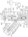
図1において、電子線検査装置は一次コラム1、二次コラム2およびチャンバー3を有している。一次コラム1の内部には、電子銃4が設けられており、電子銃4から照射される電子ビーム(一次ビーム)の光軸上に一次光学系5が配置される。また、チャンバー3の内部には、ステージ6が設置され、ステージ6上には試料Wが載置される。
In FIG. 1, the electron beam inspection apparatus has a
一方、二次コラム2の内部には、試料Wから発生する二次ビームの光軸上に、カソードレンズ8、ニューメニカルアパーチャ9、ウィーンフィルタ10、第2レンズ11、フィールドアパーチャ12、第3レンズ13、第4レンズ14および検出器15が配置される。なお、ニューメニカルアパーチャ9は、開口絞りに相当するもので、円形の穴が開いた金属製(Mo等)の薄板である。そして、開口部が一次ビームの集束位置およびカソードレンズ8の焦点位置になるように配置されている。したがって、カソードレンズ8とニューメニカルアパーチャ29とは、テレセントリックな電子光学系を構成している。
On the other hand, in the
一方、検出器15の出力は、コントロールユニット16に入力され、コントロールユニット16の出力は、CPU17に入力される。CPU17の制御信号は、一次コラム制御ユニット18、二次コラム制御ユニット19およびステージ駆動機構7に入力される。一次コラム制御ユニット18は、一次光学系5のレンズ電圧制御を行い、二次コラム制御ユニット19は、カソードレンズ8、第2レンズ11ないし第4レンズ14のレンズ電圧制御およびウィーンフィルタ10に印加する電磁界制御を行う。
On the other hand, the output of the detector 15 is input to the
また、ステージ駆動機構7は、ステージの位置情報をCPU17に伝達する。さらに、一次コラム18、二次コラム19、チャンバー3は、真空排気系(不図示)と繋がっており、真空排気系のターボポンプ等により排気されて、内部は真空状態を維持している。
The stage drive mechanism 7 transmits stage position information to the
電子銃4からの一次ビームは、一次光学系5によってレンズ作用を受けながら、ウィーンフィルタ10に入射する。ここでは、電子銃のチップとしては、矩形陰極で大電流を取り出すことができるLaB6を用いる。また、一次光学系5は、非回転対称の四重極または八重極の静電(または電磁)レンズを使用する。これは、X軸、Y軸各々で集束と発散とを引き起こすことができる。このレンズを2段、3段で構成し、各レンズ条件を最適化することによって、照射電子を損失することなく、試料面上のビーム照射領域を、任意の矩形状、または楕円形状に整形することができる。
The primary beam from the electron gun 4 is incident on the
具体的には、静電レンズを用いた場合、4つの円柱ロッド(四重極)を使用する。対向する電極同士を等電位にし、互いに逆の電圧特性を与える。
なお、四重極レンズとして円柱形ではなく、静電偏向器で、通常使用される円形板を4分割した形状のレンズを用いてもよい。この場合レンズの小型化を図ることができる。一次光学系5を通過した一次ビームは、ウィーンフィルタ10の偏向作用により軌道が曲げられる。ウィーンフィルタ10は、磁界と電界を直交させ、電界をE、磁界をB、荷電粒子の速度をvとした場合、E=vBのウィーン条件を満たす荷電粒子のみを直進させ、それ以外の荷電粒子の軌道を曲げる。一次ビームに対しては、磁界によるカFBと電界による力FEとが発生し、ビーム軌道は曲げられる。一方、二次ビームに対しては、カFBと力FEとが逆方向に働くため、互いに相殺されるので二次ビームはそのまま直進する。
Specifically, when an electrostatic lens is used, four cylindrical rods (quadrupoles) are used. Opposing electrodes are equipotential, and opposite voltage characteristics are given.
In addition, as a quadrupole lens, a lens having a shape obtained by dividing a generally used circular plate into four by an electrostatic deflector may be used instead of a cylindrical shape. In this case, the lens can be reduced in size. The orbit of the primary beam that has passed through the primary
一次光学系5のレンズ電圧は、光源像がニューメニカルアパーチャ9の開口部で結像するように、予め設定されている。すなわち、光学顕微鏡でいうケーラー照明が実現される。このニューメニカルアパーチャ9は、装置内に散乱する余計な電子ビームが試料面に到達することを阻止し、試料Wのチャージアップや汚染を防いでいる。
The lens voltage of the primary
一次ビームが試料に照射されると、試料のビーム照射面からは、二次ビームとして、二次電子、反射電子または後方散乱電子が発生する。
二次ビームは、カソードレンズ8によるレンズ作用を受けながら、レンズを透過する。
When the sample is irradiated with the primary beam, secondary electrons, reflected electrons, or backscattered electrons are generated as a secondary beam from the beam irradiation surface of the sample.
The secondary beam passes through the lens while receiving the lens action of the
ところで、カソードレンズ8は、3枚の電極で構成されている。一番下の電極は、試料Wに対して、正の電界を形成し、2次電子を引き込み、効率よくレンズ内に導くように設計されている。
Incidentally, the
また、レンズ作用は、カソードレンズ8の1番目、2番目の電極に電圧を印加し、3番目の電極をゼロ電位にすることで行われる。一方、ニューメニカルアパーチャ9は、カソードレンズ8の焦点位置、すなわち試料Wからのバックフォーカス位置に配置されている。したがって、視野中心外(軸外)から出た電子ビームの光束も、平行ビームとなって、このニューメニカルアパーチャ9の中心位置を、けられが生じることなく通過する。
The lens action is performed by applying a voltage to the first and second electrodes of the
なお、ニューメニカルアパーチャ9は、二次ビームに対しては、第2レンズ11ないし第4レンズ14のレンズ収差を抑える役割を果たしている。ニューメニカルアパーチャ9を通過した二次ビームは、ウィーンフィルタ10の偏向作用を受けずに、そのまま直進して通過する。
The
二次ビームを、カソードレンズ8のみで結像させると、倍率の色収差及び歪曲収差が発生しやすい。そこで、第2レンズ11と合わせて、1回の結像を行わせる。二次ビームは、カソードレンズ8および第2レンズ11により、フィールドアパーチャ12上で中間結像を得る。この場合、通常、二次光学系として必要な拡大倍率が、不足することが多いため、中間像を拡大するためのレンズとして、第3レンズ13、第4レンズ14を加えた構成にする。二次ビームは、第3レンズ13、第4レンズ14各々により拡大結像し、ここでは、合計3回結像する。なお、第3レンズ13と第4レンズ14とを合わせて1回(合計2回)結像させてもよい。
When the secondary beam is imaged only by the
また、第2レンズ11ないし第4レンズ14はすべて、ユニポテンシャルレンズまたはアインツェルレンズとよばれる回転軸対称型のレンズである。各レンズは、3枚電極の構成で、通常は外側の2電極をゼロ電位とし、中央の電極に印加する電圧で、レンズ作用を行わせて制御する。また、中間の結像点には、フィールドアパーチャ12が配置されている。フィールドアパーチャ12は光学顕微鏡の視野絞りと同様に、視野を必要範囲に制限しているが、電子ビームの場合、余計なビームを、後段の第3レンズ13および第4レンズ14と共に遮断して、検出器15のノイズ発生や汚染を防いでいる。なお、拡大倍率は、この第3レンズ13および第4レンズ14のレンズ条件(焦点距離)を変えることで設定される。
The second lens 11 to the fourth lens 14 are all rotational axis symmetric lenses called unipotential lenses or Einzel lenses. Each lens has a configuration of three electrodes. Usually, the outer two electrodes are set to zero potential, and the lens action is performed with a voltage applied to the center electrode. A
二次ビームは、二次光学系により拡大投影され、検出器15の検出面に結像する。検出器15は、電子を増幅するマイクロチャンネルプレート(MCP)と、電子を光に変換する蛍光板と、真空系と外部との中継および光学像を伝達させるためのレンズやその他の光学系と、撮像素子(CCD等)とから構成される。二次ビームは、MCP検出面で結像し、増幅され、蛍光板によって電子は光信号に変換され、撮像素子によって光電信号に変換される。 The secondary beam is enlarged and projected by the secondary optical system, and forms an image on the detection surface of the detector 15. The detector 15 includes a micro channel plate (MCP) that amplifies electrons, a fluorescent plate that converts electrons into light, a relay between the vacuum system and the outside, and lenses and other optical systems for transmitting optical images, and imaging It is comprised from an element (CCD etc.). The secondary beam forms an image on the MCP detection surface and is amplified, and the electrons are converted into an optical signal by the fluorescent plate and converted into a photoelectric signal by the imaging device.
コントロールユニット16は、検出器15から試料の画像信号を読み出し、CPU17に伝達する。CPU17は、画像信号からテンプレートマッチング等によってパターンの欠陥検査を実施する。また、ステージ6は、ステージ駆動機構7により、XY方向に移動可能となっている。CPU17は、ステージ6の位置を読み取り、ステージ駆動機構7に駆動制御信号を出力し、ステージ6を駆動させ、順次画像の検出、検査を行う。
The
さらに、二次ビームに対しては、試料Wからの全ての主光線が、カソードレンズ8に垂直(レンズ光軸に平行)に入射し、ニューメニカルアパーチャ9を通過するので、周辺光もけられることがなく、試料周辺部の画像輝度が低下することがない。また、電子が有するエネルギーのばらつきによって、結像する位置が異なる、いわゆる倍率色収差が起こる(特に、二次電子は、エネルギーのばらつきが大きいため、倍率色収差が大きい)が、カソードレンズ8の焦点位置に、ニューメニカルアパーチャ9を配置することで、この倍率色収差を抑えることができる。
Further, for the secondary beam, all the principal rays from the sample W are incident on the
また、拡大倍率の変更は、ニューメニカルアパーチャ9の通過後に行われるので、第3レンズ13、第4レンズ14のレンズ条件の設定倍率を変えても、検出側での視野全面に均一な像が得られる。なお、本実施例では、むらのない均一な像を取得することができるが、通常、拡大倍率を高倍にすると、像の明るさが低下するという問題点が生じた。そこで、これを改善するために、二次光学系のレンズ条件を変えて拡大倍率を変更する際、それに伴って決まる試料面上の有効視野と、試料面上に照射される電子ビームとを、同一の大きさになるように一次光学系のレンズ条件を設定する。
In addition, since the enlargement magnification is changed after passing through the
すなわち、倍率を上げていけば、それに伴って視野が狭くなるが、それと同時に電子ビームの照射エネルギー密度を上げていくことで、二次光学系で拡大投影されても、検出電子の信号密度は、常に一定に保たれ、像の明るさは低下しない。 In other words, if the magnification is increased, the field of view is narrowed accordingly, but at the same time, by increasing the irradiation energy density of the electron beam, the signal density of the detected electrons can be increased even if it is enlarged and projected by the secondary optical system. It is always kept constant and the brightness of the image does not decrease.
また、本実施例の電子線検査装置では、一次ビームの軌道を曲げて、二次ビームを直進させるウィーンフィルタ10を用いたが、それに限定されず、一次ビームの軌道を直進させ、二次ビームの軌道を曲げるウィーンフィルタを用いた構成の検査装置でもよい。また、本実施例では、矩形陰極と四極子レンズとから矩形ビームを形成したが、それに限定されず、例えば円形ビームから矩形ビームや楕円形ビームを作り出してもよいし、円形ビームをスリットに通して矩形ビームを取り出してもよい。
Further, in the electron beam inspection apparatus of the present embodiment, the
ウィーンフィルタすなわちE×B偏向器としての電子ビーム偏向部10の詳細な構造について、図2、及び図2のA−A線に沿う縦断面を示した図3を用いて説明する。図2に示すように、電子ビーム偏向部の場は、写像投影光学部(試料に電子ビームが照射されて、試料表面に応じて発生した二次電子及び反射電子の一次元像又は二次元像を電子ビーム検出器上に結像させる部分)の光軸に垂直な平面内において、電界と磁界とを直交させた構造、即ちE×B構造とする。
The detailed structure of the Wien filter, that is, the electron
ここで、電界は凹面状の曲面を持つ電極10−1及び10−2により発生させる。電極10−1及び10−2が発生する電界は、それぞれ制御部10a及び10dにより制御される。一方、電界発生用の電極10−1及び10−2と直交するように、電磁コイル10−1a及び10−2aを配置させることにより、磁界を発生させている。尚、電界発生用の電極10−1、10−2は点対象である。(同心円でも構わない。)
この場合は磁界の均一性を向上させるために、平行平板形状を有するポールピースを持たせて、磁路を形成している。A−A線に沿う縦断面における電子ビームの挙動は、図3に示されるようになる。照射された電子ビーム1aは、電極10−1及び10−2が発生する電界と、電磁コイル10−1a及び10−2aが発生する磁界とによって偏向された後、試料面上に対して垂直方向に入射する。
Here, the electric field is generated by the electrodes 10-1 and 10-2 having concave curved surfaces. The electric fields generated by the electrodes 10-1 and 10-2 are controlled by the
In this case, in order to improve the uniformity of the magnetic field, a magnetic path is formed by providing a pole piece having a parallel plate shape. FIG. 3 shows the behavior of the electron beam in the longitudinal section along the line AA. The
ここで、照射電子ビーム1aの電子ビーム偏向部10への入射位置及び角度は、電子のエネルギーが決定されると一義的に決定される。さらに、二次電子2aが直進するように、電界及び磁界の条件、即ちvB=Eとなるように電極10−1及び10−2が発生する電界と、電磁コイル10−1a及び10−2aが発生する磁界とを、それぞれの制御部10a及び10d、10c及び10bが制御することで、二次電子は電子ビーム偏向部10を直進して、写像投影光学部に入射する。ここで、Vは電子2aの速度(m/s)、Bは磁場(T)、Eは電界(V/m)である。
Here, the incident position and angle of the
次ぎに、写像投影方式を利用した欠陥検査装置の別の実施例を説明する。
写像投影方式を利用した欠陥検査装置においては、(1)電子線を一括照射するために、試料表面上でチャージアップしやすいこと、(2)本方式で得られる電子線電流に限界が有り(1.6μA程度)検査速度向上の妨げとなっているという問題点があった。
Next, another embodiment of the defect inspection apparatus using the mapping projection method will be described.
In the defect inspection apparatus using the mapping projection method, (1) it is easy to charge up on the sample surface to irradiate the electron beam at once, and (2) the electron beam current obtained by this method has a limit ( There was a problem that it hindered the improvement of the inspection speed.
本実施例では、一次電子線を複数とし、前記複数の一次電子線を二次元(X−Y方向)に走査しながら(すなわち、ラスタースキャンしながら)試料表面の観察領域を照射し、二次電子光学系に写像投影方式を採用することによって解決することができる。この実施例では、前述の写像投影方式の利点を持つとともに、この写像方式の課題である(1)電子線を一括照射するために、試料表面上でチャージアップしやすいこと、(2)本方式で得られる電子線電流に限界が有り(1.6μA程度)検査速度向上の妨げとなっていること、については、複数の一次電子線を走査することにより解決できる。即ち、電子線照射点が移動するので電荷が逃げやすく、チャージアップが減少する。また、複数の電子線の本数を増やすことにより、容易に電流値を増加できる。この実施例において、例えば、4本の一次電子線を使う場合、一本の電子線電流が500nA(電子線の径10μm)で合計2μAが得られた。16本程度には容易に一次電子線の数を増やすことが可能であり、この場合で8μAを得ることが原理的に可能である。複数の一次電子線を走査する場合、当該複数の一次電子線による照射量が、照射領域に均一になるように照射することにより、前記のようにラスタスキャンに限らず、リサージュ図形などの他の形状の走査を行うことができる。従って、ステージの走査方向は複数の電子線の走査方向に垂直である必要は無い。
In this embodiment, a plurality of primary electron beams are used, and the observation region on the sample surface is irradiated while scanning the plurality of primary electron beams in two dimensions (XY direction) (that is, while performing a raster scan). This can be solved by adopting a mapping projection method in the electron optical system. This embodiment has the advantages of the mapping projection method described above, and is a problem of this mapping method. (1) It is easy to charge up on the sample surface in order to collectively irradiate electron beams. (2) This method The fact that there is a limit to the electron beam current obtained in (1), which hinders the improvement of the inspection speed, can be solved by scanning a plurality of primary electron beams. That is, since the electron beam irradiation point moves, the charge easily escapes and the charge-up is reduced. Further, the current value can be easily increased by increasing the number of the plurality of electron beams. In this example, for example, when four primary electron beams were used, one electron beam current was 500 nA (
この実施例に用いられる電子線源として、熱電子線源(電子放出材を加熱することにより電子を放出する方式)を使用することができる。この場合も、電子放出(エミッタ)材はLaB6とすることが好ましい。高融点(高温での蒸気圧が低い)で仕事関数の小さい材料であれば、他の材料を使用することも可能である。複数の電子線を得るために、2通りの方法を用いることができる。一つは、一本のエミッタ(突起が一つ)から一本の電子線引き出し、複数の穴のあいた薄板(開ロ板)を通すことにより、複数の一次電子線を得る方法である。もう一つの方法は、一本のエミッタに複数の突起を形成してそこから直に複数の一次電子線を引き出す方法である。いずれの場合も電子線は突起の先端から放出されやすい性質を利用している。他の方式の電子線源、例えば熱電界放出型の電子線も使用可能である。熱電界放出電子線源とは、電子放出材に高電界をかけることにより電子を放出させ、更に電子線放出部を加熱することにより、電子放出を安定させた方式のことである。 As an electron beam source used in this embodiment, a thermionic beam source (a system in which electrons are emitted by heating an electron emitting material) can be used. Again, the electron emission (emitter) material is preferably a LaB 6. Other materials can be used as long as they have a high melting point (low vapor pressure at high temperature) and a low work function. Two methods can be used to obtain a plurality of electron beams. One is a method of obtaining a plurality of primary electron beams by drawing one electron beam from one emitter (one protrusion) and passing it through a thin plate (open plate) having a plurality of holes. The other method is a method in which a plurality of projections are formed on one emitter, and a plurality of primary electron beams are drawn directly therefrom. In either case, the electron beam utilizes the property of being easily emitted from the tip of the protrusion. Other types of electron beam sources such as a thermal field emission type electron beam can also be used. The thermal field emission electron beam source is a system in which electrons are emitted by applying a high electric field to the electron emission material, and the electron beam emission part is heated to stabilize the electron emission.
次に、複数の一次電子線を二次元(X−Y方向)に走査しながら(すなわち、ラスタースキャンしながら)試料表面の観察領域を照射し、二次電子光学系に写像投影方式を採用した上記実施例を図4及び図5を参照しながらより詳細に説明する。 Next, while irradiating the observation area of the sample surface while scanning a plurality of primary electron beams in two dimensions (XY direction) (that is, while performing raster scanning), a mapping projection method is adopted for the secondary electron optical system. The above embodiment will be described in more detail with reference to FIGS.
下記実施例では、複数の一次電子線を得る方法として、一本のエミッタに複数の突起を形成してそこから直に複数の一次電子線を引き出す方法を採用している。
図4に示されるように、電子銃20から放出された4本の電子線21(21−1、21−2、21−3、21−4)は開口50−1で整形され、2段のレンズ22−1、22−2でウィーンフィルタ23の偏向中心面に10μm×12μmの楕円状に結像され、図の紙面垂直方向に偏向器26によりラスタースキャンされ、4本の電子線全体として1mm×0.25mmの矩形領域を均一にカバーするように結像される。ウィーンフィルタとしてのE×B23で偏向された複数の電子線はニューメリカルアパーチャーNAでクロスオーバーを結び、レンズ24で1/5に縮小され試料Wに200μ×50μmをカバーし、かつ試料面に垂直になるように照射、投影される。試料から放出されたパターン画像(試料像F)の情報を持った4本の2次電子線25は、レンズ24、27−1、27−2で拡大され、MCP28−1上に全体として4本の電子線25で合成された矩形画像(拡大投影像F‘)として結像する。この二次電子線25による拡大投影像F’は、MCP28−1で1万倍に増感され、蛍光部28−2により光に変換され、TDI(Time Delay Integration)−CCD29で試料の連続移動速度に同期された電気信号となり、画像表示部30で連続した画像として取得され、CRT上等に出力した。
In the following embodiment, as a method for obtaining a plurality of primary electron beams, a method is adopted in which a plurality of projections are formed on a single emitter and a plurality of primary electron beams are directly extracted therefrom.
As shown in FIG. 4, the four electron beams 21 (21-1, 21-2, 21-3, 21-4) emitted from the
電子線照射部は試料表面をできるだけ均一に、かつ照射むらを少なくして、矩形状に電子線で照射する必要があり、また、スループットをあげるためにはより大きな電流で照射領域を電子線照射する必要がある。従来の電子線照射むらは±10%程度であり画像のコントラストむらが大きく、また、電子線照射電流は照射領域において500nA程度と少ないために、高いスループットが得られないという問題があった。また、走査型電子線顕微鏡(SEM)方式に比べて、本方式は広い画像観察領域を一括して電子線照射するためにチャージアップによる結像障害が生じやすいという問題があった。 The electron beam irradiation unit needs to irradiate the sample surface with the electron beam in a rectangular shape with uniform uniformity as much as possible and with less irradiation unevenness. There is a need to. Conventional non-uniformity of electron beam irradiation is about ± 10%, and the non-uniformity of image contrast is large. Further, since the electron beam irradiation current is as small as about 500 nA in the irradiation region, there is a problem that high throughput cannot be obtained. In addition, compared with the scanning electron microscope (SEM) method, this method has a problem in that an image formation failure due to charge-up is likely to occur because a large image observation area is collectively irradiated with an electron beam.
本実施例の一次電子線照射方法を図5に示す。一次電子線21は、4本の電子線21−1、21−2、21−3、21−4で構成されている。、それぞれのビームは2μm×2.4μmの楕円状しており、それぞれ1本当り200μm×12.5μmの矩形領域をラスタースキャンし、それらが重なり合わないように足し合わせて全体として200μm×50μmの矩形領域を照射する。21−1のビームは21−1’ヘ有限の時間で到達し次にビームスポット径分(10μm)ずれた21−1の直下(21−2方向)にほとんど時間損失なしに戻り、再度前記と同じ有限の時間で21−1〜21−1’に平行に21−1’の直下(21−2’方向)に移動し、これを繰り返して図の点線で示す矩形の照射領域の1/4(200μm×12.5μm)を走査した後はじめの点21−1に戻りこれを高速に繰り返す。他の電子線21−2〜21−4も電子線21−1と同様に同じ速度で走査を繰り返し、全体として図の矩形の照射領域(200μm×50μm)を均一に高速に照射する。均一に照射できれば、前記のラスタースキャンでなくても良い。例えばリサージュ形を描くように走査しても良い。従って、ステージの移動方向は図に示す方向Aである必要は無い。即ち、ステージの移動方向はスキャン方向(図の横方向の高速走査方向)に垂直である必要は無い。本実施例では電子線照射むらは±3%程度で照射できた。照射電流は1本の電子線当たり250nAで試料表面で全体として、4本の電子ビームで1.0μAを得ることができた(従来の2倍)。電子線の本数を増やすことにより、電流を増加でき、高スループットを得ることができる。また、照射点が従来に比べて小さく(面積で約1/80)また移動しているのでチャージアップは従来の1/20以下に抑えることができた。
A primary electron beam irradiation method of this example is shown in FIG. The
図中には示していないが、本装置には、レンズの他に、制限視野絞り、電子線の軸調整のための4極またはそれ以上の極数を有する偏向器(アライナー)、非点収差補正器(スティグメータ)、さらにビーム形状を整形する複数の4重極レンズ(4極子レンズ)等電子線の照明、結像に必要なユニットを備えている。 Although not shown in the figure, in addition to the lens, this apparatus includes a limited field stop, a deflector (aligner) having four or more poles for adjusting the axis of the electron beam, astigmatism. A unit necessary for illumination and imaging of an electron beam such as a corrector (stigmator) and a plurality of quadrupole lenses (quadrupole lenses) for shaping the beam shape are provided.
次に、写像投影方式の電子線検査装置の別の実施例を説明する。当該実施例に係る電子線検査装置は、試料(例えばウェハ若しくはマスク)特に、最小線幅が0.1μm以下のデバイスパターンを有するウェハ等の欠陥検査を、高いスループットでかつ高い信頼性で行えるようにしたものである。 Next, another embodiment of a projection type electron beam inspection apparatus will be described. The electron beam inspection apparatus according to the embodiment can perform defect inspection of a sample (for example, a wafer or a mask), particularly a wafer having a device pattern with a minimum line width of 0.1 μm or less, with high throughput and high reliability. It is a thing.
まず、本実施例の概要について説明する。
本実施例に係る写像投影方式の電子線検査装置は、電子銃から放出した電子線を矩形の電子ビームに成形し、その電子ビームをウェハの表面に照射し、ウェハ面から放出された二次電子の像を検出器に結像させる。このような写像投影方式の欠陥検査用の電子線検査装置は、走査型電子顕微鏡のビームスポット径よりも大きい矩形状又は面状のビームを使用し、その照射領を一括して結像させ、画像を取得する。従って、走査型に比べて高いスループット化の要求を満足させることができる。また、この装置においては、ステージを連続的に移動させてウェハ全面を走査することによりウェハから放出された二次電子を蛍光板で光学的像に変換し、変換された像をラインセンサ(TDI−CCD)で撮像する。
First, an outline of the present embodiment will be described.
The mapping projection type electron beam inspection apparatus according to this embodiment forms an electron beam emitted from an electron gun into a rectangular electron beam, irradiates the surface of the wafer with the electron beam, and emits a secondary light emitted from the wafer surface. An electron image is formed on the detector. An electron beam inspection apparatus for defect inspection of such a mapping projection method uses a rectangular or planar beam that is larger than the beam spot diameter of a scanning electron microscope, forms an image of the irradiation area at once, Get an image. Accordingly, it is possible to satisfy the demand for higher throughput than the scanning type. In this apparatus, the stage is continuously moved to scan the entire surface of the wafer, so that secondary electrons emitted from the wafer are converted into an optical image by a fluorescent screen, and the converted image is converted into a line sensor (TDI-). CCD).
このようなラインセンサでは、図9に示されているように、直交した2軸の1軸方向(図で左右方向)にC1ないしCnのライン状に並べられているn個のCCD画素列が他の軸方向(図で上下方向)にROW−1ないしROW−mのm個並べられて、CCDアレイを構成している。各CCD画素列に蓄積された電荷は外部からの一垂直クロック信号により一度に垂直方向へCCD一画素分だけ転送される(即ち電荷が矢印Eの方向に移動する)。ある時点でROW−1に撮像されたn個の画素のライン画像は、クロック信号が与えられたときにROW−2に転送される。続けてクロック信号が与えられるとROW−2に転送されたライン画像は垂直方向に更に一画素分だけ移動しROW−3に転送される。こようにして画像の移動に追従してROW−mまで電荷の転送が繰り返し行われて最終的に水平出力レジスタから画像データとしてラインセンサの外部に取り出される。 In such a line sensor, as shown in FIG. 9, n CCD pixel columns arranged in a line of C1 to Cn in one axis direction (two directions in the figure) of two orthogonal axes are arranged. A CCD array is configured by arranging m pieces of ROW-1 to ROW-m in other axial directions (vertical direction in the figure). The charge accumulated in each CCD pixel column is transferred by one CCD pixel in the vertical direction at a time by one vertical clock signal from the outside (that is, the charge moves in the direction of arrow E). A line image of n pixels captured by ROW-1 at a certain time is transferred to ROW-2 when a clock signal is given. When a clock signal is subsequently applied, the line image transferred to ROW-2 is further moved by one pixel in the vertical direction and transferred to ROW-3. In this way, following the movement of the image, the charge transfer is repeatedly performed up to ROW-m, and finally it is taken out of the line sensor as image data from the horizontal output register.
しかしながら、ラインセンサの電荷移動時間(以下、ラインレートと呼ぶ)を一定として撮像を行うと、ステージの移動速度の変動に伴って走査型電子顕微鏡方式による欠陥検査装置では問題とならないラインセンサの電荷移動の非同期に起因した像ぼけを生じる。更に、ウェハ全面検査に伴う焦点機構により電子光学系の倍率変動が生じ、ウェハ上の画素サイズが変化するために最適ラインレートが変動し、それにより同様な像ぼけが生じる。 However, when imaging is performed with the charge transfer time (hereinafter referred to as the line rate) of the line sensor being constant, the charge of the line sensor that does not cause a problem in the defect inspection apparatus using the scanning electron microscope system due to fluctuations in the moving speed of the stage. This causes image blur due to asynchronous movement. Furthermore, the magnification mechanism of the electron optical system changes due to the focus mechanism associated with the entire wafer inspection, and the optimum line rate changes because the pixel size on the wafer changes, thereby causing the same image blur.
本実施例の一つの目的は、ラインセンサのラインレートを常にステージの移動速度と同期させ、電荷移動の非同期により生じる像ぼけを回避することができる欠陥検査用の電子線検査装置を提供することである。 One object of the present embodiment is to provide an electron beam inspection apparatus for defect inspection that can always synchronize the line rate of the line sensor with the moving speed of the stage and avoid image blur caused by asynchronous movement of charges. It is.
本実施例の他の目的は、電子光学系の倍率変動に伴う像ぼけを回避することができる欠陥検査用の電子線検査装置を提供することである。
そこで、本実施例に係る写像投影方式の欠陥検査用の電子線検査装置では、電子銃から放出された電子線を所望の形状に成形し、該成形された電子ビームを検査されるべき試料面上に照射する一次電子光学系と、前記試料から放出された二次電子を結像する二次電子光学系と、前記結像された二次電子像を蛍光板を介して光学像に変換し、ラインセンサで検出させる検出器とを備えた写像投影型の欠陥検査用の電子線検査装置において、前記ラインセンサに設けられた画素列において撮像されたライン画像を転送するときの電荷移動時間を、試料を移動させるステージの移動速度に連動して制御する制御装置を設けている。ステージの移動速度を検出し、最適なラインレートを算出してフィードバックすることにより、ラインセンサのラインレートを常にステージの移動速度と同期させ、電荷移動の非同期により生じる像ぼけを回避することができる。
Another object of the present embodiment is to provide an electron beam inspection apparatus for defect inspection that can avoid image blur due to magnification fluctuation of an electron optical system.
Therefore, in the electron beam inspection apparatus for defect inspection of the projection method according to the present embodiment, the electron beam emitted from the electron gun is formed into a desired shape, and the formed electron beam is to be inspected on the sample surface. A primary electron optical system that irradiates on, a secondary electron optical system that forms an image of secondary electrons emitted from the sample, and the imaged secondary electron image is converted into an optical image via a fluorescent plate; In the projection type electron beam inspection apparatus for defect inspection provided with a detector to be detected by a line sensor, a charge transfer time when transferring a line image captured in a pixel column provided in the line sensor, A control device is provided for controlling in conjunction with the moving speed of the stage for moving the sample. By detecting the moving speed of the stage, calculating the optimum line rate, and feeding it back, the line rate of the line sensor is always synchronized with the moving speed of the stage, and image blur caused by asynchronous charge movement can be avoided. .
また、本実施例に係る電子線検査装置の一つ変形例では、前記ラインセンサの電荷移動時間を前記電子光学系の倍率の変動に連動して制御するように構成されている。それにより、ウェハ全面検査に伴う焦点機構により電子光学系の倍率変動が生じた場合でも、電荷移動の非同期により生じる像ぼけを回避することができる。 Further, in one modification of the electron beam inspection apparatus according to the present embodiment, the charge transfer time of the line sensor is controlled in conjunction with the fluctuation of the magnification of the electron optical system. Thereby, even when the magnification variation of the electron optical system is caused by the focus mechanism accompanying the wafer whole surface inspection, it is possible to avoid the image blur caused by the asynchronous movement of the charge.
また、他の変形例において、前記二次電子光学系の二次電子を倍増するために、前記蛍光板の前段にマイクロチャンネルプレートを配置している。
また、他の変形例において、前記ステージの位置を測定するためのレーザ干渉計を備えている。それにより、ステージの位置情報をレーザ干渉計から検出し、ステージの移動速度から最適なラインレートを算出してフィードバックすることができ、ラインセンサのラインレートを常にステージの移動速度と同期させ、電荷移動の非同期により生じる像ぼけを回避することができる。
In another modification, in order to double the secondary electrons of the secondary electron optical system, a microchannel plate is disposed in front of the fluorescent plate.
In another modification, a laser interferometer for measuring the position of the stage is provided. As a result, the position information of the stage can be detected from the laser interferometer, the optimum line rate can be calculated from the stage moving speed and fed back, and the line rate of the line sensor can be always synchronized with the stage moving speed, Image blur caused by asynchronous movement can be avoided.
以下図面を参照して、本実施例に係る写像投影方式の欠陥検査用の電子線検査装置をより具体的に説明する。
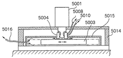
図6において、本実施例の欠陥検査用の電子線検査装置1001が模式的に示されている。この欠陥検査用の電子線検査装置1001は、電子銃から放出された電子線を所望の形状(例えば、矩形、若しくは楕円形等)に成形し、成形された電子ビームを検査されるべき試料(例えばウェハ若しくはマスク等、本実施例においては以下ウェハと呼ぶ)Sの表面上に照射する一次電子光学系1002と、ウェハSから放出された二次電子を検出器に拡大投影する二次電子光学系1003と、二次電子を受けて光の像に変換し、更に電気信号に変換する検出器1004と、検出器1004を制御するための制御装置1005(図7)とを備えている。
With reference to the drawings, the electron beam inspection apparatus for defect inspection of the projection method according to the present embodiment will be described more specifically below.
FIG. 6 schematically shows an electron
一次電子光学系1002は、電子線1021を放出する電子銃1022と、電子線1021を所定の断面形状のビームに成形する一次系静電レンズ1023とを備え、それらは、図6に示すように、ウェハSの表面に垂直な方向に対し一定の角度を有していて、電子銃1022を最上部にして順に配置されている。一次電子光学系1002は更に、電界と磁界とが直交する場により電子ビームを偏向すると共にウェハSからの二次電子を分離するためのE×B分離器1024と、静電対物レンズ1025とを備え、これらはウェハSの表面に垂直な方向に沿って配置されている。
The primary electron
二次電子光学系1003は、E×B分離器1024で分離されたウェハSからの二次電子1031の光軸Aに沿って、ウェハSの表面に対して垂直な方向に配置されており、二次電子を拡大投影する二次系静電レンズ1032を備えている。
The secondary electron
検出装置1004は、MCP(マイクロチャンネルプレート)1041と、二次電子光学系からの二次電子を光の像に変換する蛍光板1042と、該光の像を検出するラインセンサ1043と、検出されたウェハ画像情報を格納するメモリー1044と、ウェハ画像を表示するCRTモニター1045とを備えている。
The
制御装置1005は、図7において示されているように、ステージの位置を測定するレーザー干渉計1051と、レーザー干渉計1051からの位置信号を変換するA/D変換器1052と、レーザー干渉計1051からの位置信号に基づいて最適ラインレートを演算し出力するラインレート制御部1053と、ラインレート制御部1053からの出力信号を変換するD/A変換器1054と、ラインレート制御部1053からの信号に基づいてラインセンサー1043を制御するラインセンサー制御部1055とを備えている。
As shown in FIG. 7, the
上記各構成要素は公知のものであってもよく、それらの構造の詳細説明は省略する。
上記構成の電子線検査装置100において、電子銃1022から放出された電子は、加速されて電子ビーム1021として一次系静電レンズ1023でその断面形状が矩形状又は楕円状に成形される。成形された電子ビームは、E×B分離器1024の偏向主面より僅かに上側で矩形又は楕円の像を結像するようにされる。E×B分離器1024に入射し結像したビーム像は、そこでウェハSの表面に垂直な方向に偏向され、静電対物レンズ1025により縮小減速されてウェハS上を照射する。
Each of the above constituent elements may be known ones, and a detailed description of their structure is omitted.
In the electron
電子ビームの照射によってウェハSから放出された二次電子1031は、静電対物レンズ1025で収束されE×B分離器1024に入射される。E×B分離器1024により二次系静電レンズ1032の方向に向けられた二次電子線は、二次系静電レンズ1032を通過し、更にMCP1041上に拡大投影される。
The
MCP1041に入射した二次電子1031はそこで増倍されて、蛍光板1042を照射する。蛍光板1042に照射された二次電子1031はそこで光の像に変換される。この画像はラインセンサ1043により検出され、電気信号に変換される。電気信号に変換されたウェハ画像データは、光ファイバーケーブルを介してウェハ画像情報としてパーソナルコンピュータのメモリー1044に格納される。このウェハ画像情報はCRTモニターに表示されて欠陥が検出される。
The
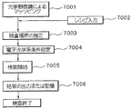
次に、制御装置1005の作用について図6及び図7を参照して説明する。検査されるウェハSはX−Yステージ1006の上に配置されている。上記で説明したような方法でウェハを検査する場合において、X−Yステージ1006を一定速度でY方向に移動させ、X−Yステージ駆動速度とウェハ上のピクセルサイズから算出されるラインレートを定数としてラインセンサ制御部1055に設定し、ラインセンサ1043の画像をCRTモニター1045に表示させる。同期がとれていない場合、X−Yステージの速度変動と同期したステージ走査方向に垂直なステージ速度とラインレートとの非同期に起因する縞模様が数本生成されて、像ぼけが生じることとなる。
Next, the operation of the
そのような縞模様による像ぼけを解消するべく、制御装置1005は以下のような制御を行う。X−Yステージ1006の移動位置はレーザー干渉計で測定され、そのシリアル出力信号はクロック周波数200メガヘルツ、16ビットでA/D変換器1052によりデジタル信号に変換され、現在のステージの位置情報Xtがラインレート制御部1053に出力される。それと共に、ラインレート制御部1053には1サイクル前の位置情報Xt−1及び遅延時間も入力される。ラインレート制御部1053は、これらの位置情報と遅延時間からステージの速度成分を算出し、更に、ステージの速度成分及びウェハ上の画素サイズから最適ラインレートの計算を行い、それらの情報信号を出力する。この出力信号はクロック周波数200メガヘルツ、16ビットでD/A変換器1054でアナログ信号に変換され、ラインセンサ制御部1055に入力される。ラインセンサ1043のラインレートはラインセンサ制御部1055からの信号により制御される。ラインセンサ制御部1055のコマンドによりラインセンサ1043のラインレートを更新して、画像の像ぼけを回避することが可能となる。この場合、X−Yステージの振動周期が数マイクロ秒より十分大きいことに対して、入出力を含む制御装置1005全体の時間遅れは十分に小さい。
In order to eliminate such image blur due to the stripe pattern, the
本実施例による上記電子線検査装置を使用してウェハの実際の検査を行った。図8において、約130mm×130mmのウェハ検査領域S1の左上の検査開始点S2をまず電子ビーム1021の照射領域の中心に移動させた後、XーYステージ1006を+Y方向に10mm/secで移動しながらウェハの検査を行った。従って、ウェハ検査領域S1は矢印Bの方向に検査される。次に、XーYステージ1006を−X方向に移動させた後、−X方向に500ミクロンほどステップ移動させる。従って、ウェハ検査領域S1は矢印Cの方向に移されることとなる。次に、XーYステージ1006を−Y方向に移動させながらウェハの検査を行った。この場合ウェハ検査領域S1は矢印Dの方向に検査される。このようにして、走査を繰り返しながらウェハ検査領域S1の全面の検査を行った。
The wafer was actually inspected using the electron beam inspection apparatus according to this example. In FIG. 8, the upper left inspection start point S2 of the wafer inspection area S1 of about 130 mm × 130 mm is first moved to the center of the irradiation area of the
検査開始点S2からXーYステージ1006を+Y方向にステージ速度10mm/secで移動しながら走査を行ったときには、ステージ速度変位±10%程度の変動を周期2.5ミリ秒毎に繰り返した。この場合、300キロヘルツ付近の周波数を有するラインレートは、ラインレート制御部1053によってステージの速度変位と同期した振動を繰り返すことにより、像ぼけのない良好な画像を取得することができた。
When scanning was performed while moving the
また、XーYステージ1006を−Y方向にステージ速度10mm/secで移動しながら走査を行ったときも、+Y方向に走査を行ったときと同様なステージ速度変位を示したが、同様な制御を行うことにより良好な画像を取得することができた。
Also, when scanning was performed while moving the
本実施例によれば、以下のような効果を奏する。
(1)ラインセンサのラインレートを制御するラインセンサ制御部の外部入力に、ラインレート制御部で算出した最適なラインレート信号をフィードバックすることにより、ラインセンサのラインレートがXーYステージの移動速度と常時同期し、ラインセンサの電荷移動遅延により生じる像ぼけを回避することができる。
(2)ウェハ全面検査に伴う自動焦点機構により電子光学系の倍率変動が生じた場合でも、ラインセンサ制御部の外部入力に、ラインレート制御部で算出した最適なラインレート信号をフィードバックすることにより、電荷移動の非同期により生じる像ぼけを回避することができる。
(3)XーYステージの振動、又はXーYステージ駆動モータの速度変動に伴うラインセンサによる画像の像ぼけを能動的に制御できる。
According to the present embodiment, the following effects can be obtained.
(1) By feeding back the optimum line rate signal calculated by the line rate control unit to the external input of the line sensor control unit that controls the line rate of the line sensor, the line rate of the line sensor is moved by the XY stage. It is always synchronized with the speed, and image blur caused by the charge transfer delay of the line sensor can be avoided.
(2) Even when the magnification change of the electron optical system occurs due to the automatic focusing mechanism accompanying the wafer whole surface inspection, the optimum line rate signal calculated by the line rate control unit is fed back to the external input of the line sensor control unit. In addition, it is possible to avoid image blur caused by asynchronous charge transfer.
(3) It is possible to actively control image blur due to the line sensor accompanying the vibration of the XY stage or the speed fluctuation of the XY stage drive motor.
次ぎに、写像投影方式の電子線検査装置の別の実施例を説明する。当該実施例に係る電子線検査装置は、多目的な電子線検査装置に関する。
まず、本実施例に係る写像投影方式の電子線検査装置の関連技術について説明する。
Next, another embodiment of a projection type electron beam inspection apparatus will be described. The electron beam inspection apparatus according to the embodiment relates to a multipurpose electron beam inspection apparatus.
First, a related technique of the electron beam inspection apparatus of the projection type according to the present embodiment will be described.
写像投影方式の電子線検査装置は、一般に1つの電子線照射部を有する。この場合、電子線を試料表面に対し斜め方向から電子線を照射し試料表面に垂直の方向から電子線を取り出すと、試料表面の凹凸により陰影が生じる問題があるので、ウイーンフィルタ(E×Bフィルタ)を用いて斜め方向の電子線を偏向し試料表面に対し垂直方向に入射するようにし、一方試料からの二次電子は、試料表面から垂直方向に取出し、偏向を受けないようにウイーンフィルタの電界及び磁界の強度を設定している。 A projection type electron beam inspection apparatus generally has one electron beam irradiation unit. In this case, if the electron beam is irradiated obliquely with respect to the sample surface and the electron beam is taken out from the direction perpendicular to the sample surface, there is a problem that shadows are generated due to the unevenness of the sample surface. Filter) to deflect the electron beam in an oblique direction so that it is incident on the sample surface in a vertical direction, while secondary electrons from the sample are taken out from the sample surface in a vertical direction so as not to be deflected. The electric field and magnetic field strengths are set.
図10は、関連する技術の写像投影型電子線検査装置装置2034の構成を示すブロック図である。この電子線検査装置2034は、試料2110に1次電子線2102を照射する電子銃2001、1次電子線2102の照射により試料表面から発生した2次電子2111を検出し画像信号を生成する検出部2114、電極2106及び磁石2107を備えるウイーンフイルタ2105、1次電子線2102を成形する第1レンズ系2003及び第2レンズ系2004、ウイーンフイルタ2105と試料2110との間に配置される第3レンズ系2108及び第4レンズ系2109、ウイーンフイルタ2105と検出部2114との間に配置される第6レンズ系2112及び第7レンズ系2113を備える。この電子線検査装置において、ウイーンフイルタ2105は、電子銃2001から照射された一次電子線2102を偏向するが試料表面から放出される2次電子2111は直進するように設定され、照射一次電子線2102を試料表面へ垂直に入射させている。このような装置は、例えば、特開平11−132975号公報に開示される。
FIG. 10 is a block diagram showing a configuration of a mapping projection type electron
このような電子線検査装置は、単機能であり、ウエハのサイズが8インチ、12インチ、15インチと大型化するにつれて電子線検査装置の床面積が大きくなり、しかも種々の検査や測定を行う必要があるため、クリーンルームに占める電子線検査装置の床面積の割合が増加する問題を生じている。 Such an electron beam inspection apparatus has a single function. As the wafer size increases to 8 inches, 12 inches, and 15 inches, the floor area of the electron beam inspection apparatus increases, and various inspections and measurements are performed. Since it is necessary, there is a problem that the ratio of the floor area of the electron beam inspection apparatus to the clean room increases.
本実施例一つの目的は、1台の電子線検査装置で複数の機能を有する電子線検査装置を提供し、少ない電子線検査装置台数でプロセス途中のウエハの検査を可能にすることである。本実施例の他の目的は、複数の機能を有する電子線検査装置を備えることにより半導体製造設備のクリーンルームに占める電子線検査装置の床面積の割合を減少することである。本実施例のその他の目的及び利点は、以下の説明において明らかにされる。 One object of the present embodiment is to provide an electron beam inspection apparatus having a plurality of functions with a single electron beam inspection apparatus, and to enable inspection of a wafer during the process with a small number of electron beam inspection apparatuses. Another object of the present embodiment is to reduce the proportion of the floor area of the electron beam inspection apparatus in the clean room of the semiconductor manufacturing facility by providing an electron beam inspection apparatus having a plurality of functions. Other objects and advantages of the present embodiment will be clarified in the following description.
そこで、本実施例に係る写像投影方式の欠陥検査用の電子線検査装置では、1次電子線を試料に照射し試料表面から発生する2次電子を検出することにより試料表面の状態を検査する多目的電子線検査装置であって、1次電子線を発生する電子源、1次電子線を整形するレンズ系、1次電子線を走査する光学系、試料を支持する試料ステージ、2次電子を検出器へ向かわせる光学系、及び2次電子を検出して画像信号を生成する検出器を有し、試料表面の欠陥検出、試料表面の欠陥レビュー、パターン線幅測定、及びパターン電位測定の内少なくとも2つの機能を有する。2つの機能は、試料表面の欠陥検出、及び試料表面の欠陥レビューであることができる。 Therefore, in the electron beam inspection apparatus for defect inspection of the projection method according to the present embodiment, the state of the sample surface is inspected by irradiating the sample with the primary electron beam and detecting secondary electrons generated from the sample surface. A multi-purpose electron beam inspection apparatus, an electron source that generates a primary electron beam, a lens system that shapes the primary electron beam, an optical system that scans the primary electron beam, a sample stage that supports the sample, and a secondary electron It has an optical system that goes to the detector, and a detector that detects secondary electrons and generates an image signal. Among the sample surface defect detection, sample surface defect review, pattern line width measurement, and pattern potential measurement It has at least two functions. The two functions can be sample surface defect detection and sample surface defect review.
本実施例に係る多目的電子線検査装置において、試料表面の欠陥検出が画像信号により得られる画像をパターンデータと比較するか又はダイ同士の画像を比較することにより行われ、試料表面の欠陥レビューがウエハ表面上における1次電子線の走査と同期させたモニター上のビームの走査により得られる画像観察により行われ、パターン線幅測定がウエハ表面上における1次電子線の走査がパターンの短辺方向に行われそのときの2次電子像により行われ、パターン電位測定が試料表面に最も近い電極に負の電位を与え試料表面の高い電位を持つパターンから放出される2次電子を選択的に試料側へ追い戻すことにより行われることができる。 In the multipurpose electron beam inspection apparatus according to the present embodiment, the defect detection on the sample surface is performed by comparing the image obtained by the image signal with the pattern data or by comparing the images of the dies, and the defect review on the sample surface is performed. The pattern line width measurement is performed by observing the image obtained by scanning the beam on the monitor in synchronization with the scanning of the primary electron beam on the wafer surface, and the scanning of the primary electron beam on the wafer surface is performed in the short side direction of the pattern. The secondary electron image obtained at that time is used for pattern potential measurement, and a negative potential is applied to the electrode closest to the sample surface, and the secondary electrons emitted from the pattern having a high potential on the sample surface are selectively sampled. Can be done by driving back to the side.
1次電子線を試料に照射し試料表面から発生する2次電子を検出することにより試料表面の状態を検査する本実施例に係る多目的電子線検査装置は、1次電子線を矩形、円形、及びスポットの内の少なくとも2種類に整形可能なレンズ系、電子線を任意の方向に走査するための偏向系を有する1次電子光学系、試料から放出される2次電子を試料表面から検出器へ向わせる検出系を有し、欠陥を自動的に検出する機能及び欠陥の位置情報を出力する機能を有し、更に上記欠陥の形状を観察可能にする機能を有する。検出系は、写像投影光学系を含むものであることができる。また検出系は、2次電子倍増管を含むものであり得る。 The multipurpose electron beam inspection apparatus according to the present embodiment, which inspects the state of the sample surface by irradiating the sample with a primary electron beam and detecting secondary electrons generated from the sample surface, And a lens system that can be shaped into at least two of the spots, a primary electron optical system having a deflection system for scanning an electron beam in an arbitrary direction, and a secondary electron emitted from the sample is detected from the sample surface And a function for automatically detecting a defect and a function for outputting position information of the defect, and a function for allowing the shape of the defect to be observed. The detection system can include a mapping projection optical system. The detection system may include a secondary electron multiplier.
本実施例に係る多目的電子線検査装置の組合せは、当該多目的電子線検査装置を1以上の列に複数台ずつ配置し、それらの試料ステージを共通とし共通の試料ステージ上の試料を検査可能とする。また多目的電子線検査装置の各々が複数の1次電子線を試料へ照射するものであることができる。このような組合せにより検査工程のスループット(単位時間当たりの検査量)を高めることがきる。 The combination of the multi-purpose electron beam inspection apparatuses according to the present embodiment is such that a plurality of the multi-purpose electron beam inspection apparatuses are arranged in one or more rows, and the samples on the common sample stage can be inspected by sharing the sample stages. To do. Further, each of the multipurpose electron beam inspection apparatuses can irradiate a sample with a plurality of primary electron beams. Such a combination can increase the throughput of the inspection process (inspection amount per unit time).
以下図面を参照して、本実施例に係る欠陥検査用の多目的電子線検査装置をより具体的に説明する。
図11は、多目的電子線検査装置2030を示す概要図である。電子線検査装置2030は、一次電子線2102を発生する電子銃2001等を収容する鏡筒2028及び鏡筒2028の下方を覆うシールドケース2029を備える。シールドケース2029は、ウエハ(試料)2110を収容し、鏡筒の下方と連通され、鏡筒内と同様に排気され真空にされる。鏡筒2028は、その内部に、電子銃2001、一次電子線2102をウエハ表面2110へ照射するためのコンデンサレンズ2002、2003、2004、矩形開口2005、円形開口2006、レンズ2024、2025、偏向器2007、ウイーンフィルタ2009、一次電子線が照射されるウエハ表面2110から放出される2次電子に作用するレンズ系2012、2010、2015、2017、マイクロチャンネルプレート2018、シンチレータ2018’、光ファイバー束2019を収容する。シールドケース2029は、ステンレスで作った場合は別途磁気遮蔽が必要であり、強磁性体で作った場合は磁気遮蔽を無くすことも可能にされる。
Hereinafter, the multipurpose electron beam inspection apparatus for defect inspection according to the present embodiment will be described more specifically with reference to the drawings.
FIG. 11 is a schematic diagram showing a multipurpose electron
電子線検査装置2030において、電子銃2001から放出された一次電子線2102は、コンデンサレンズ2002、2003、2004、矩形開口2005、円形開口2006、レンズ2024、2025、偏向器2007、ウイーンフィルタ2009等を通り、ウエハ(試料)表面1110へ照射される。電子銃2001から放出された一次電子線2102は、コンデンサレンズ2002、2003、2004で収束され、矩形開口2005又は後方の円形開口2006を一様な強度で照射する。図11の装置においては、レンズ2024及び2025を調整することにより、ウエハ表面2110上に、矩形開口2005の縮小像、円形開口2006の縮小像又はクロスオーバーの縮小像を選択形成可能にされる。また偏向器2007を作動させることにより、ウエハ表面上で一次電子線2102を走査することが可能になっている。
In the electron
図11の電子線検査装置2030において、ウエハ表面の画像は、次のように作成される。即ち、一次電子線2102が照射されたウエハ表面2110から放出される2次電子が、レンズ系2012、2010、2015、2017を経てマイクロチャンネルプレート2018上に結像され、その後面のシンチレータ2018’で光の像に変換され、光ファイバー束2019、2020で外部へ取出され、2次元CCD2027により電気信号に変換され画像が作成される。この作成された画像をパターンデータと比較(自動パターン整合手順)したり、隣りのダイ(すなわち、同じウェーハ上に配列された隣のチップ)の同じ場所で作成された画像同志を比較する、即ちダイ同志を比較する(欠陥比較処理機)ことによって欠陥を自動的に検出し、欠陥位置を出力(欠陥後処理機)できる。このように、電子線検査装置2030は、写像投影方式の電子線検査装置の機能を有している。
In the electron
図11の電子線検査装置2030において、モニター2023の輝度変調は次のように行う。即ち、ウエハ表面2110に隣接するレンズ2012に特定の電圧を与えることにより、2次電子の軌道2014をウエハ表面の縁部に隣接する2次電子倍増管2021へ向け、2次電子を2次電子倍増管2021で増幅し、得られた電気信号を増幅器2022により増幅し、モニター2023の輝度変調に用いる。
In the electron
図11の電子線検査装置2030において、ウエハ表面の欠陥の観察は、次のようにして行うこともできる。即ち、偏向器2007を作動させウエハ表面2110上での一次電子線2102の走査と同期してモニター2023のビームを走査し、得られた画像、即ちSEM画像とパターンデータによる画像とを比較することによりウエハ表面の欠陥の観察を行う。このように、電子線検査装置2030は、走査型電子ビーム方式(SEM方式)を用いた電子線検査装置の機能をも有している。したがって、偏向器2007を作動させて、ウエハ表面上で一次電子線を矩形又は長方形のパターンの例えば短辺方向に走査することにより、モニター2023で得られた2次電子像により長辺方向に沿って配列されたパターン線幅を測定するができる。
In the electron
また、電子線検査装置2030を写像投影方式として用いた場合でも、走査型電子ビーム方式として用いた場合でも、ウエハ表面2110に隣接するレンズ2012の最もウエハに近い方の電極2012aに負の電位を与えることによって、ウエハ表面の高い電位を持つパターンから放出された2次電子を選択的にウエハ側へ追い戻すことによって、パターンの電位を評価して、ウェーハに生じた電気的な導通不良(オープン、ショート不良など)、すなわち、コンタクト不良をより正確に検査することができる。
In addition, even when the electron
電子線検査装置2030の写像投影方式と走査型電子ビーム方式との切換は、制御装置2900により行うことができるようになっている。
本実施例多目的電子線検査装置は、上述のように、1台の装置により、欠陥検出、欠陥レビュー、パターン線幅測定、パターン電位測定等多目的の検査及び測定を行うことができるので、クリーンルーム内に多くの床面積を占めることがなく、それ故、デバイス製造装置を多く配置することができ、クリーンルームの有効利用を図ることができる。
The
Since the multi-purpose electron beam inspection apparatus of this embodiment can perform multi-purpose inspection and measurement such as defect detection, defect review, pattern line width measurement, and pattern potential measurement with a single apparatus as described above, Therefore, a large number of device manufacturing apparatuses can be arranged and effective use of the clean room can be achieved.
次ぎに、写像投影方式の電子線検査装置の別の実施例を説明する。当該実施例に係る電子線検査装置は、最小線幅が0.1ミクロン以下の高密度パターンの形状観察や欠陥検査を高精度且つ高信頼性で行うのに適した電子線検査装置に関するものである。 Next, another embodiment of a projection type electron beam inspection apparatus will be described. The electron beam inspection apparatus according to the embodiment relates to an electron beam inspection apparatus suitable for performing shape observation and defect inspection of a high-density pattern having a minimum line width of 0.1 microns or less with high accuracy and high reliability. is there.
上記のように、半導体デバイスの高密度化に伴ない、半導体ウェーハ等の基板の表面の欠陥を高精度に検査する必要が生じ、これに応えるものとして、写像投影型電子線検査装置が提案されている。この写像投影型電子線検査装置は、試料の表面に電子銃から一次電子線を照射し、それによって試料から生成された二次電子線をマイクロチャンネルプレートに結像させて電子を増倍した後、シンチレータによって電子線をその強度を表す光に変換し、これをTDI−CCDで検出して電気信号へ変換し、この電気信号を試料の走査に同期させることにより、連続した画像を得るものである。 As described above, with the increase in the density of semiconductor devices, it becomes necessary to inspect defects on the surface of a substrate such as a semiconductor wafer with high precision, and as a response to this, a projection type electron beam inspection apparatus has been proposed. ing. This projection type electron beam inspection device irradiates the surface of a sample with a primary electron beam from an electron gun, thereby forming a secondary electron beam generated from the sample on a microchannel plate and multiplying electrons. The scintillator converts an electron beam into light representing its intensity, detects it with a TDI-CCD, converts it into an electrical signal, and synchronizes this electrical signal with the scanning of the sample, thereby obtaining a continuous image. is there.
しかしながら、こうした写像投影型の電子線検査装置においては、ステージの移動方向をTDI−CCDの受光面の配列方向と精度良く一致させる必要があり、その精度は、製作時の加工精度や組立て精度等の機械的精度に依存している。しかし、近年の0.1ミクロン以下の形状観察や欠陥検査を対象とする装置においては、関連する技術では、必要とする精度を達成することが困難であるという問題があった。 However, in such a projection type electron beam inspection apparatus, it is necessary to accurately match the moving direction of the stage with the arrangement direction of the light receiving surface of the TDI-CCD. Depends on the mechanical accuracy of However, in recent apparatuses that are intended for shape observation and defect inspection of 0.1 μm or less, there is a problem that it is difficult to achieve the required accuracy with the related technology.
本実施例は、機械的精度で達成することが不可能であった、試料の走査方向とTDI−CCD受光面の配列方向との高精度のアラインメントを達成可能にし、信頼性の高い形状観察及び欠陥検査を行うことができる電子線検査装置を提供することを目的とする。 The present embodiment makes it possible to achieve a highly accurate alignment between the scanning direction of the sample and the arrangement direction of the TDI-CCD light receiving surface, which could not be achieved with mechanical accuracy, and enables reliable shape observation and An object of the present invention is to provide an electron beam inspection apparatus capable of performing defect inspection.
そこで、本実施例に係る写像投影方式の欠陥検査用の電子線検査装置では、一次電子線により試料を照射する電子照射部と、該一次電子線の照射により前記試料から生成された二次電子線を光学的に処理して前記試料の画像を生成する光学系と、該画像を受け取るマイクロチャンネルプレートと、該マイクロチャンネルプレートの出力をシンチレータで光に変換した後、該光信号を電気信号へ変換するCCDと、該CCDの出力を処理する画像表示部と、前記試料を移動させるステージとを備えてなり、前記ステージによって前記試料を走査する電子線検査において、前記試料と前記マイクロチャンネルプレートとの間に、前記画像を回転させる磁気レンズが配置されている。 Therefore, in the electron beam inspection apparatus for defect inspection of the projection method according to the present embodiment, an electron irradiation unit that irradiates the sample with a primary electron beam, and secondary electrons generated from the sample by irradiation with the primary electron beam An optical system that optically processes lines to generate an image of the sample, a microchannel plate that receives the image, and an output of the microchannel plate is converted into light by a scintillator, and then the optical signal is converted into an electrical signal. A CCD for conversion, an image display unit for processing the output of the CCD, and a stage for moving the sample. In the electron beam inspection in which the sample is scanned by the stage, the sample, the microchannel plate, In between, a magnetic lens for rotating the image is arranged.
前記磁気レンズは、前記光学系の終段のレンズと前記マイクロチャンネルプレートとの間に位置してもよい。
前記磁気レンズは、前記マイクロチャンネルプレートに最も近いクロスオーバー位置に配置してもよい。
The magnetic lens may be positioned between a final lens of the optical system and the microchannel plate.
The magnetic lens may be disposed at a crossover position closest to the microchannel plate.
前記磁気レンズは、前記終段のレンズに関して前記マイクロチャンネルプレートとは反対側の前記終段のレンズに最も近い結像位置に配置してもよい。
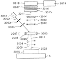
図12は、本実施例に係る電子線検査装置の構成を概略的に示す図で、該電子線検査装置は写像投影型の電子線検査装置として実現されている。同図において、電子線検査装置は電子銃3001を備え、電子銃3001から放出された一次電子線3002は矩形の開口で整形され、2段のレンズ3003、3004を経て、電極3005と磁石3006とを有するウィーン・フィルタ3007に入射する。このとき、一次電子線3002は、ウィーン・フィルタ3007の面に例えば1mm×0.25mm角で結像される。ウィーン・フィルタ3007で一次電子線3002は進路を変更され、レンズ3008、3009を通過して1/5に縮小された後、ステージS上の試料3010に垂直に投影される。試料3010は、例えばウェーハであり、その表面には回路パターンが形成されている。
The magnetic lens may be disposed at an imaging position closest to the final lens on the side opposite to the microchannel plate with respect to the final lens.
FIG. 12 is a diagram schematically showing the configuration of the electron beam inspection apparatus according to the present embodiment, and the electron beam inspection apparatus is realized as a mapping projection type electron beam inspection apparatus. In the figure, the electron beam inspection apparatus includes an
一次電子線3002によって照射されて、試料3010の表面から二次電子線が放出され、また、一次電子線3002の一部は試料3010の表面で反射される。これらの反射電子線及び二次電子線3011は、試料3010上の回路パターンを表す情報を含んでいる。二次電子線3011はレンズ3009、3008を経てウィーン・フィルタ3007を直進し、一次電子線3002の経路から外れた経路を経て静電型レンズ系のレンズ3012、3013を通過する。二次電子線3011はレンズ3009、3008、3012、3013によって拡大される。
Irradiated by the
静電型レンズ系の最終段のレンズ3013から出た二次電子線3011は磁気レンズ3014を通った後、マイクロチャンネルプレート3015上に矩形の像として結像する。ここに磁気レンズ3014を配置した理由については後述する。結像された矩形の像はマイクロチャンネルプレート3015によって1万倍に増感されて蛍光部3016を照射する。これにより、蛍光部3016は増感された矩形の画像を光に変換し、変換された光はリレー光学系3017を経てTDI−CCD3018を照射する。そこで、TDICCD3018は入射した光を、試料3010を移動ステージによって走査する走査速度に同期した電気信号へ変換し、連続した画像として画像処理部3019へ与える。
The
こうして画像処理部3019により取得された画像は、オンタイムでの複数のセルの画像比較や複数のダイの画像の比較による試料3010の表面の欠陥の検出に供される。画像処理部3019で検出された試料3010上の欠陥の形状の特徴、数及び位置座標等は、必要に応じて、CRT上に表示され、また記録される。
The image thus acquired by the
なお、上記の試料表面の形状観察や欠陥検査においては、試料3010の基板が例えば酸化膜や窒化膜が用いられることがあって表面構造が違うことや、製造工程が異なることを考慮して、適切な条件の下で荷電粒子を試料3010に照射し、最適な照射条件で照射を行った後、画像を取得して形状観察や欠陥検査を行うことが望ましい。
In the above-described sample surface shape observation and defect inspection, considering that the substrate of the
さらに、2次電子だけでなく散乱電子や反射電子による画像も上記のように取得できるが、ここでは2次電子画像を取得した場合について述べている。
ここで、図13を用いて、図12に示す磁気レンズ1304の動作原理を説明する。磁気レンズ1304は、上から見て環状の形状をしていると共に、その横断面は左右にU字形状が表される形状となっている。図13の(A)及び(B)は、磁気レンズ1304の中心部分のみを表した図である。図13の(A)及び(B)に示すように、磁気レンズ3014のポールピースの中心を二次電子線3011が通過するとき、上側のポールピース3021aと下側のポールピース3021bとの間に配置された図示しない環状のコイルにより上下のポールピースを通って磁路が形成されて、二次電子線3011に磁界が印加され、それによって、二次電子線3011は、二次電子線3011の光軸中心に対して矢印3022で示す方向に回転させられる。このときの二次電子線3011の回転量は、ポールピース3021a及びbを通って二次電子線3011に印加される磁界を強くすればするほど大きくなる。
Further, not only secondary electrons but also images by scattered electrons and reflected electrons can be acquired as described above. Here, a case where a secondary electron image is acquired is described.
Here, the principle of operation of the magnetic lens 1304 shown in FIG. 12 will be described with reference to FIG. The magnetic lens 1304 has an annular shape when viewed from above, and has a cross-sectional shape that represents a U-shape on the left and right. FIGS. 13A and 13B show only the central portion of the magnetic lens 1304. FIG. As shown in FIGS. 13A and 13B, when the
この原理を利用すると、例えば、磁気レンズ3014をレンズ3013とマイクロチャンネルプレート3015との間に配置し、磁気レンズ3014が発生する磁界の強度を調整することにより、試料3010から放出された二次電子線3011がマイクロチャンネルプレート3015上に結像したときの画像を回転させることができる。したがって、磁気レンズ3014の磁界強度の調整により、移動ステージSで試料3010を走査するときの走査方向とTDI−CCD3018の受光面の積算方向とを一致させることが可能になる。
Using this principle, for example, the
また、磁気レンズ3014を静電型レンズ系の最終段のレンズ3013とマイクロチャンネルプレート3015との間に配置すると、静電型レンズ系に対して影響(例えば、静電型レンズ系の倍率を変えてしまったり、収差や歪みを生じさせたりすること)を与えることなく、磁気レンズ3014による二次電子線3011の回転、したがって、結像画像の回転を行うことができる。
Further, when the
実際、図12に示すように、磁気レンズ3014を最終段のレンズ3013とマイクロチャンネルプレート3015との間に配置した場合、試料3010の走査方向とTDICCD3018の受光面の配列方向とを予め機械的に±1度以内に調整した後、磁気レンズ3014の磁界強度を変えて二次電子線の回転角度を測定したところ、二次電子線の回転を±10秒以内の角度で行い得ることがわかった。これは、角度精度が、(視野寸法/2)×(角度精度)<(1/10)×(ピクセル寸法)の関係を満たせばよく、したがって、角度精度<(1/2048×5)rad=9.77×10−5rad=20.2秒であることによる。
In fact, as shown in FIG. 12, when the
上で説明した磁気レンズ3014は、図14又は図15に示す位置に配置されることが望ましい。図14は、これまで説明したとおり、磁気レンズ3014は、静電型レンズ系の最終段のレンズ3013とマイクロチャンネルプレート3015との間の、レンズ3013に最も近いクロスオーバー位置3031に配置される。これにより、磁気レンズ3014の二次電子線に対する回転作用が利用でき、しかも写像投影系の静電レンズ系の合焦条件に与える影響を殆ど無視し得る位にすることができる。
The
一方、図15においては、磁気レンズ3014は、静電型レンズ系の最終段のレンズ3013に関してマイクロチャンネルプレート3015とは反対の側の、レンズ3013に最も近い結像位置3041に配置される。結像位置3041は、試料3010の表面及びマイクロチャンネルプレート3015の二次電子線入射面と共役の位置であり、磁気レンズ3014の回転作用以外のいかなるレンズ作用も働かない位置である。このため、磁気レンズ3014は、試料3010の走査方向とTDI−CCD3018の受光面の配列方向とのずれを補正する作用を行うだけである。換言すると、磁気レンズ3014により、こうした方向のずれを容易に補正することができる。また、磁気レンズ3014による回転作用により写像投影系の静電型レンズ系が影響されて収差や歪みを生じることがないので、図14に示す配置と同等又はそれ以上の優れた精度を達成することができる。
On the other hand, in FIG. 15, the
以上、本実施例に係る電子線検査装置の説明から理解されるように、この実施例は、試料の走査方向とTDI−CCDの受光面の配列方向とを容易に一致させることができるので、これらの方向の不一致に起因する画像のぼけを除去又は最小化することができ、分解能が0.1ミクロン以下という優れた分解能の下で信頼性の高い形状観察や欠陥検査が可能になるという格別の効果を奏する。 As described above, as can be understood from the description of the electron beam inspection apparatus according to the present embodiment, this embodiment can easily match the scanning direction of the sample and the arrangement direction of the light receiving surface of the TDI-CCD. It is possible to eliminate or minimize image blur caused by these direction mismatches, and to enable highly reliable shape observation and defect inspection with excellent resolution of 0.1 micron or less. The effect of.
また、この実施例においては、TDI−CCDの段数を増やしても、試料に対する走査の方向とTDI−CCD受光面の配列方向との不一致による画像ボケが少ないため、一層高い段数のTDI−CCDを使用することが可能になり、一層高感度の電子線検査を提供することができ、したがって高スループットを実現することができるという効果も奏される。 In this embodiment, even if the number of stages of TDI-CCD is increased, image blur due to inconsistency between the scanning direction of the sample and the arrangement direction of the TDI-CCD light receiving surface is small. It can be used, and an electron beam inspection with higher sensitivity can be provided. Therefore, an effect that a high throughput can be realized is also achieved.
次ぎに、電子線検査装置の別の実施例を説明する。本実施例は、単一又は複数の電子線を使用し固体試料表面の評価を行う電子線検査装置に関し、特に最小線幅0.1μm以下のパターンを有するウエハ、マスク等の試料の評価を、高スループット(時間当たり処理量)、高精度、高信頼性をもって行う電子線検査装置に関する。評価項目は、半導体ウエハ等の試料の欠陥検査、線幅測定、重ね精度測定、高時間分解能の電位コントラスト測定等である。電位コントラスト測定は、ウエハの表面下の電気的な欠陥や、ウエハ表面上の微小粒子の測定を可能にするものである。 Next, another embodiment of the electron beam inspection apparatus will be described. This example relates to an electron beam inspection apparatus that evaluates the surface of a solid sample using a single or a plurality of electron beams, and in particular, evaluates samples such as wafers and masks having a pattern with a minimum line width of 0.1 μm or less. The present invention relates to an electron beam inspection apparatus that performs with high throughput (processing amount per hour), high accuracy, and high reliability. Evaluation items include defect inspection of a sample such as a semiconductor wafer, line width measurement, overlay accuracy measurement, potential contrast measurement with high time resolution, and the like. The potential contrast measurement enables measurement of electrical defects below the wafer surface and fine particles on the wafer surface.
本実施例において、電子線の寸法Dは、電子線の試料表面上の像の径寸法(直径又は対角線長)を意味するものとする。また、本実施例において、電子線の間隔は、隣接する電子線の試料表面上における隣接する像の中心間の距離を意味するものとする。 In this embodiment, the dimension D of the electron beam means the diameter dimension (diameter or diagonal length) of the image of the electron beam on the sample surface. In the present embodiment, the interval between electron beams means the distance between the centers of adjacent images on the sample surface of adjacent electron beams.
まず、本実施例に係る電子線検査装置の関連技術について説明する。
ウエハの被評価試料の欠陥等を評価する、この種の電子線検査装置は、例えば、特開平9−311112号公報に開示される。この公報は、1次電子線をマスク、ウエハ等のパターンが形成された被検査試料に照射し被検査試料からの2次電子を利用するパターン検査装置を開示する。また、関連技術においては、対物レンズと被検査試料の間に減速電界を印加し、1次電子線を細く絞り被検査試料に照射し被検査試料からの2次電子を高率良く検出している。また、半球状のメッシュから成る2次電子エネルギーフィルターを利用して試料の表面のパターンの電位コントラストを測定している。
First, the related technique of the electron beam inspection apparatus according to the present embodiment will be described.
This type of electron beam inspection apparatus for evaluating defects or the like of a sample to be evaluated on a wafer is disclosed, for example, in Japanese Patent Laid-Open No. 9-311112. This publication discloses a pattern inspection apparatus that uses a secondary electron from a sample to be inspected by irradiating a sample to be inspected, such as a mask or a wafer, with a primary electron beam. In the related art, a deceleration electric field is applied between the objective lens and the sample to be inspected, the primary electron beam is narrowed down and irradiated on the sample to be inspected, and secondary electrons from the sample to be inspected are detected with high efficiency. Yes. Further, the potential contrast of the pattern on the surface of the sample is measured using a secondary electron energy filter made of a hemispherical mesh.
この種の関連技術で用いられている減速電界型対物レンズは、2次電子を全て通過させるので電位コントラストを測定することが困難である。また半球状のメッシュ電極から成る2次電子フィルターは、対物レンズと試料間にメッシュ電極を設けると対物レンズの像面距離が長くなり、軸上色収差係数が大きくなる問題、及び1次電子線ビームを細く絞ることができないか又は細く絞ろうとするとビーム電流が小さくなる問題を有する。更にメッシュ電極は、メッシュの近傍を通る1次電子線の軌道を不規則に曲げるので、ビームがボケを生じたり、走査歪が生じる問題を有する。 The decelerating electric field type objective lens used in this type of related technology passes all secondary electrons, so it is difficult to measure the potential contrast. In addition, the secondary electron filter composed of a hemispherical mesh electrode has a problem that if the mesh electrode is provided between the objective lens and the sample, the image plane distance of the objective lens becomes long, and the axial chromatic aberration coefficient becomes large. Cannot be narrowed down, or there is a problem that the beam current becomes small when trying to narrow down. Further, since the mesh electrode irregularly bends the trajectory of the primary electron beam passing through the vicinity of the mesh, there is a problem that the beam is blurred or scanning distortion occurs.
本実施例の目的は、このような関連技術の問題に鑑みなされたものであり、1次電子線を細く絞りながら大きなビーム電流を得ることができ、電位コントラストの測定が可能であり走査歪のない電子線検査を提供することにある。 The purpose of the present embodiment is made in view of such problems of the related art. A large beam current can be obtained while narrowing down the primary electron beam, potential contrast can be measured, and scanning distortion can be reduced. There is no electron beam inspection to provide.
本実施例の電子線検査は、少なくとも3枚の軸対称電極を有する単ポテンシャル静電レンズ、即ち電子銃に近い側の電極(上側電極)、試料に近い方の電極(試料側電極、下側電極)及び両者の間の中央電極、を有する静電レンズによって試料表面に1次電子線を合焦させ偏向器で1次電子線を走査させることによって試料から発生する2次電子を検出し試料表面の評価を行う。電子線検査は、下側電極に試料表面より低い電位の電圧を与えることによって試料表面上のパターンの電位コントラストを得るようにしている。 The electron beam inspection of this example is performed by using a single potential electrostatic lens having at least three axisymmetric electrodes, that is, an electrode closer to the electron gun (upper electrode), and an electrode closer to the sample (sample side electrode, lower side). Electrode) and a central electrode between them, the primary electron beam is focused on the sample surface by the electrostatic lens, and the secondary electron generated from the sample is detected by scanning the primary electron beam with the deflector. The surface is evaluated. In the electron beam inspection, a potential contrast of a pattern on the sample surface is obtained by applying a lower voltage to the lower electrode than the sample surface.
本実施例の電子線検査においては、電位コントラストを得る必要のない評価を行う時、試料側電極(下側電極)に対してアースに近い電圧が与えられる。また、下側電極に与える電圧を大きく変化した時の合焦条件の調整は、中央電極に与える正の高圧を変えることにより行われる。 In the electron beam inspection of the present embodiment, when an evaluation that does not require obtaining a potential contrast is performed, a voltage close to ground is applied to the sample side electrode (lower electrode). In addition, the adjustment of the focusing condition when the voltage applied to the lower electrode is greatly changed is performed by changing the positive high voltage applied to the center electrode.
本実施例の電子線検査においては、合焦条件を高速で小変化させる時は、静電レンズの中央電極より電子銃側の電極(上側電極)に与える電圧を調整して行う。本実施例においては、電位分布を与えられた試料表面からの2次電子の発生の変化により、コントラスト像が得られる。 In the electron beam inspection of the present embodiment, when the focusing condition is slightly changed at high speed, the voltage applied to the electron gun side electrode (upper electrode) from the central electrode of the electrostatic lens is adjusted. In this embodiment, a contrast image is obtained by a change in the generation of secondary electrons from the sample surface to which a potential distribution is given.
以下、図面を参照して、本実施例の具体的な内容を詳細に説明する。図16は、本実施例に係る電子線検査の概略構成を示す概要図である。図16に示すように、電子銃4020は、ウエーネルト4021の内部に配置されるカソード4022、ウエーネルト4021の下部に配置されるアノード4023を備え、1次電子線がカソード4022からアノード4023に向けて放出され、アノード4023を通過した電子線は、軸合せ偏向器4024、4025で軸合せされ、コンデンサレンズ4034、4035、4036の中心を通るようにされる。
Hereinafter, the specific contents of the present embodiment will be described in detail with reference to the drawings. FIG. 16 is a schematic diagram illustrating a schematic configuration of the electron beam inspection according to the present embodiment. As shown in FIG. 16, the
カソード4022が、熱電界放出カソード(TEFカソード)である場合は、カソード4022から放出された1次電子線は、コンデンサレンズ4034、4035、4036によって試料表面への結像倍率が調整され1次電子線4016とされ、対物レンズ4032、4038、4039で試料4033の表面へ合焦される。そして1次電子線4016は、E×B分離器4030の偏向中心にクロスオーバを作り、静電偏向器4027及びE×B分離器4029、4030の内電磁偏向器4029により2段偏向され、試料4033の表面上をラスタ走査する。
When the cathode 4022 is a thermal field emission cathode (TEF cathode), the primary electron beam emitted from the cathode 4022 has its imaging magnification on the sample surface adjusted by
図16の電子線検査において、試料の検査は、1次電子線により試料33の表面x方向(図16において紙面に垂直方向)の所定幅をx方向に走査しながらステージ4041をy方向へ連続移動させて行われる。試料のy方向の端まで(一定の領域)の検査が終了すると、ステージ4041をx方向へ所定幅又はそれより僅かに大きい幅だけ移動させ、隣のストライプ(隣接する領域)を検査する。1次電子線4016が試料4033の表面上をラスタ走査で照射することにより試料4033の走査点から2次電子が放出される。
In the electron beam inspection of FIG. 16, the inspection of the sample is performed by continuously scanning the
試料4033上の照射点から放出された2次電子は、対物レンズ4031の中央電極4039の高電圧、上側電極4038及び下側電極4032の接地電圧、並びに試料4033の負の高電圧で形成される2次電子に対する加速電界により電子銃側へ引上げられ、E×B分離器4029、4030で1次光学系から偏向され図16の点線の方向の軌道を取り、2次電子線検出器4028で検出され、SEM像(走査型電子顕微鏡像)が形成される。試料4033の電位コントラストを評価する場合は、対物レンズ4031の試料側電極4032に試料電位より低い電位の電圧を与えることによって、軸上ポテンシャル分布を次に述べる図18のように試料の表面より低くなるようにする。図16に示す制御装置4900により、所望の電位の電圧を、上側電極4038、中央電極4039及び下側電極4032にそれぞれ与えることができるようになっている。
Secondary electrons emitted from the irradiation point on the
図18は、上側電極4038、中央電極4039、下側電極4032、及び試料4033に、それぞれ4.5kV、8kV、350V、500Vをそれぞれ与えた時の軸上ポテンシャルの分布を示す。図18において、横軸は、Z軸、すなわち試料4033の面に対して垂直に伸びる軸線の距離を表しており、基準点の0mmは、上側電極4038から前記軸線に向けて垂直に伸びる線と前記軸線との交点となっている。したがって、図中の4.000mmは、前記交点からの距離を示している。図18において、図示されていないが、点4002の対応する位置に試料4033が配置されており、点4001と点4002との間の中央位置に対応する位置に下側電極4032が配置されており、点4003の対応する位置に中央電極4039が配置されている。下側電極4032に試料電位より低い電位の電圧が与えられているので、図18の点4001と点4002の範囲で軸上ポテンシャルが試料33の表面より低くなっている。2次電子の内の高い電位を持つパターンから発生したものは、ポテンシャルエネルギーが低くその速度が低いことから、点4001と点4002間のポテンシャル障壁により、試料側へ追い戻され検出されない。一方、2次電子の内の低い電位を持つパターンから発生したものは、ポテンシャルエネルギーが高くより大きな速度を持っているので、このポテンシャル障壁を越えて検出器28へ達する。
FIG. 18 shows on-axis potential distributions when 4.5 kV, 8 kV, 350 V, and 500 V are applied to the
試料側(下側)電極4032に試料よりも低い電位を与えると、中央電極4039と下側電極4032の間に大きい電界が発生するので、両者の間は、上側電極4038と中央電極4039の間より広くする方がよい。また中央電極4039と下側電極4032との間の電界が大きくなることにより、レンズ作用が強くなり過ぎ、合焦条件が大きくずれることになる。これを補正するためには、中央電極4039に与える正の高電圧を大きく変化させ、より低い電圧を与えれば良い。
When a potential lower than that of the sample is applied to the sample side (lower)
図16の電子線検査におけるレンズ構造(コンデンサレンズ4034、4035、4036)は、一体のセラミックス4026から削り出して作り、その表面に選択的に金属をコーティングすることによって電極を形成することにより、鏡筒4040の外径を小さくすることができる。図17は、小さくした外径の鏡筒4040を4筒×2列に配置した様子を示す。図17の例では、2次電子検出器4028を隣接する光学系と干渉しない側へ向け、8インチのウエハ上に8本の鏡筒4040を配置した。図17の8本の鏡筒4040(各々の外径が40mmφ以下の場合)の配置により、試料ステージ4041をy方向へ移動させながら評価を行うと、単一の鏡筒4040を使用する場合の8倍のスループット(時間当り処理量)を得ることができる。
The lens structure (
試料4033のパターン段差や材質の差で画像を作る場合は、2次電子検出効率は、大きい方が良い。その場合は、試料側電極4032にはアースに近い電位を与えれば良い。その時の中央電極4039に与える電圧は、正の高電圧となる。また試料の表面の凹凸等に応答させるためダイナミックに焦点合せを行う場合は、アースに近い電圧の上側電極4038に与える電圧を調整する。この場合は、制御電圧を高速で変化させることが可能である。
In the case where an image is created based on the pattern level difference or material difference of the
なお、本実施例の電子線検査装置は、走査型電子ビーム方式(SEM方式)の電子線検査装置として説明したが、本実施例の特徴部分は、写像投影型の電子線検査装置にも適用可能である。 The electron beam inspection apparatus according to the present embodiment has been described as a scanning electron beam type (SEM type) electron beam inspection apparatus. However, the characteristic part of the present embodiment is also applicable to a mapping projection type electron beam inspection apparatus. Is possible.
本実施例の電子線検査装置は、3枚の軸対称電極を有する静電レンズの試料に近い方の電極に試料表面より低い電位の電圧を与えることによって、対物レンズの像面距離が長くなり軸上色収差係数が大きくなることや1次電子線ビームを細く絞ることができない等の問題を生じることがない。この場合、1次電子線の試料表面への合焦は、中央電極に与える正の高圧を変えることにより調整保持される。電位コントラストを得る必要のない時は、試料に近い側の電極にアースに近い電圧を与えることにより2次電子の検出を効率良く行うことができる。 In the electron beam inspection apparatus of this embodiment, the image plane distance of the objective lens is increased by applying a voltage having a lower potential than the sample surface to the electrode closer to the sample of the electrostatic lens having three axisymmetric electrodes. There is no problem that the axial chromatic aberration coefficient becomes large or the primary electron beam cannot be narrowed down. In this case, the focusing of the primary electron beam on the sample surface is adjusted and held by changing the positive high voltage applied to the center electrode. When it is not necessary to obtain potential contrast, secondary electrons can be detected efficiently by applying a voltage close to ground to the electrode on the side close to the sample.
次に、本発明の別の実施例を説明する。本実施例は、2次元又は3次元の方向に移動可能なステージ(以下、単にステージと呼ぶ)上に設置された試料に対して荷電ビームとしての電子線を照射する荷電ビーム装置、及びステージ上に試料を搬送する方法に関する。 Next, another embodiment of the present invention will be described. In this embodiment, a charged beam apparatus that irradiates an electron beam as a charged beam onto a sample placed on a stage (hereinafter simply referred to as a stage) movable in a two-dimensional or three-dimensional direction, and on the stage The present invention relates to a method for transporting a sample.
まず、本実施例に係る荷電ビーム装置の関連技術について説明する。
ステージ上に設置された試料に対して荷電ビームを照射する、この種の荷電ビーム装置としての電子線装置においては、荷電ビームの通路全体を真空環境にする必要性から、ステージ全体を真空容器内に設置している。また、真空中でステージを機能させるには、大気中でステージを作動させるのと異なり、ステージのアクチュエータ、ガイド部の支持構造や潤滑、及び材料等に特別の配慮が必要であった。
First, the related technology of the charged beam apparatus according to the present embodiment will be described.
In this type of electron beam apparatus that irradiates a specimen placed on a stage with a charged beam, the entire stage is placed in a vacuum vessel because the entire path of the charged beam needs to be in a vacuum environment. It is installed in. Also, in order to make the stage function in a vacuum, special considerations are required for the stage actuator, the guide support structure, lubrication, materials, and the like, unlike when the stage is operated in the atmosphere.
例えば、アクチュエータに関しては、真空中にサーボモータを配置する場合には、放熱が困難であるためサーボモータを高温仕様にしたりサーボモータの仕様条件に制限を設ける必要が生じたり、回転軸の潤滑に固体潤滑剤や真空グリスを使用しなければならない。一方、大気側にサーボモータを配置する場合には、回転導入部に磁性流体シール等の真空シール機構を設けると共に、ステージにX方向とY方向のガイドの他にもう一段のガイドを設けて、サーボモータがX方向またはY方向のガイドと共に移動することを要しない構造にする必要があり、大気中で作動するステージに比べて構造が複雑で大型になっていた。 For example, regarding the actuator, when the servo motor is placed in a vacuum, it is difficult to dissipate heat, so it may be necessary to set the servo motor to a high temperature specification or to limit the specification conditions of the servo motor, or to lubricate the rotating shaft. Solid lubricant or vacuum grease must be used. On the other hand, when the servo motor is arranged on the atmosphere side, a vacuum seal mechanism such as a magnetic fluid seal is provided at the rotation introduction part, and another stage guide is provided on the stage in addition to the X direction and Y direction guides. It is necessary to make the structure that does not require the servo motor to move with the guide in the X direction or the Y direction, and the structure is more complicated and larger than the stage that operates in the atmosphere.
ガイド部の支持構造に関しては、大気中で使用される高精度のステージに対して使用されるような静圧を利用した空気軸受が、真空環境のもとでは使用できない。また、クロスローラーベアリング等の高精度転がり軸受を使用する場合においても、大気中で用いられる潤滑剤よりも潤滑性が劣る真空グリスや、低蒸気圧のフッ素系潤滑油を、潤滑剤として使用しなければならなかった。このため、真空用の高精度ステージを製作するのが困難であった。 Regarding the support structure of the guide portion, an air bearing using a static pressure as used for a high-precision stage used in the atmosphere cannot be used in a vacuum environment. In addition, when using high-precision rolling bearings such as cross roller bearings, vacuum grease that is inferior to lubricants used in the atmosphere or fluorine-based lubricants with low vapor pressure are used as lubricants. I had to. For this reason, it has been difficult to produce a high-precision stage for vacuum.
ステージの材料に関しては、真空中での放出ガス量が少ない材料を選定する必要があり、アルミニウム材はあまり使用されず、また、材料の表面積を小さくするために部品表面の仕上げにも格別の配慮を必要としていた。 Regarding the material of the stage, it is necessary to select a material that emits a small amount of gas in a vacuum. Aluminum material is not often used, and special consideration is given to the finish of the part surface in order to reduce the surface area of the material. Needed.
真空用のステージ機構には、上記の他にも、ステージを内蔵する真空容器、試料を大気中から真空環境内に移送するためのロードロック室、試料の真空搬送機構、真空容器の真空配管、バルブ類、及び真空ポンプ等が必要であった。 In addition to the above, the vacuum stage mechanism includes a vacuum container with a built-in stage, a load lock chamber for transferring the sample from the atmosphere to the vacuum environment, a sample vacuum transfer mechanism, a vacuum pipe for the vacuum container, Valves, a vacuum pump, etc. were required.
また、試料は真空中に載置されるので、試料を固定する方法として吸着力で固定するような真空チャックが使用できず、静電チャックまたは試料の表面もしくは側面を固定子で押さえる機械式チャックを使用しなければならなかった。しかしながら、静電チャックには、高価かつパーティクルを吸着し易く、一部のタイプの静電チャックでは除電に時間を要するといった問題点があり、一方、機械式チャックには、平坦に保持する事が不可能な上に試料の表面または側面を固定子で押さえなければならず、試料であるウェハの裏面以外にチャックを接触させたくないという半導体メーカの要求を満足できないという問題点があった。 In addition, since the sample is placed in a vacuum, a vacuum chuck that is fixed by adsorption force cannot be used as a method of fixing the sample, and an electrostatic chuck or a mechanical chuck that presses the surface or side of the sample with a stator. Had to use. However, electrostatic chucks are expensive and easy to adsorb particles, and some types of electrostatic chucks require time for static elimination. On the other hand, mechanical chucks can be held flat. In addition to this, there is a problem that the surface or side surface of the sample must be pressed by a stator and the semiconductor manufacturer's requirement that the chuck does not want to contact other than the back surface of the sample wafer cannot be satisfied.
以上に述べたように、関連する荷電ビーム装置は、ステージを真空環境内に設けなければならないため、装置の製造コストが高く、大きな設置面積や占有面積を必要とし、機構が複雑で装置の保守管理も困難であった。 As described above, the related charged beam apparatus requires a stage to be provided in a vacuum environment, so the manufacturing cost of the apparatus is high, a large installation area and an occupied area are required, the mechanism is complicated, and the apparatus is maintained. Management was also difficult.
更に、一般的には、大気に曝された物体を真空排気すると、その表面に吸着されたガス分子が離脱してくるため、所定の真空度を得るためにはある程度の排気時間を必要とする。この離脱してくるガスのほとんどは、高い真空度では水分子(即ち、大気中で表面に吸着した水蒸気)である。従って、大気に曝された試料を十分に真空排気せずに荷電ビーム照射領域に搬送した場合には、荷電ビーム照射領域の真空環境内に搬送された途端に試料面に吸着されていたガス分子が放出されて、荷電ビーム照射領域の真空度を悪化させてしまい、求められる所定の性能での処理が行えないという問題点も従来からあった。従って、試料面やステージの構成部品の表面から荷電ビーム照射領域内に放出されるガスの量を大幅に減少させかつ放出ガスを迅速に排気することが求められている。 Furthermore, in general, when an object exposed to the atmosphere is evacuated, gas molecules adsorbed on the surface are released, so that a certain amount of evacuation time is required to obtain a predetermined degree of vacuum. . Most of the desorbed gas is water molecules (that is, water vapor adsorbed on the surface in the atmosphere) at a high degree of vacuum. Therefore, when the sample exposed to the atmosphere is transferred to the charged beam irradiation region without being sufficiently evacuated, the gas adsorbed on the sample surface as soon as it is transferred into the vacuum environment of the charged beam irradiation region. Conventionally, there has been a problem that molecules are emitted and the degree of vacuum in the charged beam irradiation region is deteriorated, so that it is impossible to perform processing with a predetermined performance. Therefore, it is required to significantly reduce the amount of gas released from the sample surface and the surface of the component parts of the stage into the charged beam irradiation region and to exhaust the released gas quickly.
本実施例の一つの目的は、ステージのアクチュエータやガイド機構等の構造を大気中に設けることにより、荷電ビーム装置をコンパクトで低い製造コストで製造可能なものとすることである。 One object of the present embodiment is to provide a charged beam apparatus that is compact and can be manufactured at a low manufacturing cost by providing a structure such as an actuator of a stage and a guide mechanism in the atmosphere.
他の目的は、試料や荷電ビームの光学系といった真空環境が必要な箇所のみを真空に維持して、試料及び荷電ビーム光学系等がパーティクルや放出ガスで汚染されないようにすることである。 Another object is to maintain only a portion where a vacuum environment is necessary, such as a sample and a charged beam optical system, so that the sample and the charged beam optical system are not contaminated by particles or emitted gas.
別の目的は、試料面やステージの構成部品の表面から真空中に放出されるガスの量を従来より大幅に減少させることができる荷電ビーム装置を提供することである。
さらに、別の目的は、試料面やステージの構成部品の表面から真空中に放出されるガスの量を従来より大幅に減少させることができるような、荷電ビーム装置内に試料を搬送する方法を提供することである。
Another object is to provide a charged beam apparatus that can significantly reduce the amount of gas released into the vacuum from the surface of a sample surface or a component of a stage.
Furthermore, another object is to provide a method for transporting a sample into a charged beam apparatus that can significantly reduce the amount of gas released into the vacuum from the surface of the sample surface or the components of the stage. Is to provide.
本実施例に係る荷電ビーム装置においては、ステージ上に置かれた試料の表面に荷電ビームを照射する装置において、荷電ビームが照射される箇所の近傍のみを所定の真空度に保つために、荷電ビームが照射される領域を中心として少なくとも一重の差動排気構造を設け、さらに、前記差動排気構造の外周側に、不活性ガスを試料面に対して噴出する構造を設けるようにしている。このように構成したことにより、ステージは大気中で使用するものを利用できることとなり、荷電ビーム装置をコンパクトで低い製造コストで製造可能なものとすることができる。更に、大気側から試料面にパーティクルが侵入することを防止すると共に、試料が大気に直接触れる機会を減少させることができ、荷電ビーム照射領域での放出ガスを減少させることができる。 In the charged beam apparatus according to the present embodiment, in the apparatus for irradiating the surface of the sample placed on the stage with the charged beam, the charge beam is maintained in order to keep only the vicinity of the portion irradiated with the charged beam at a predetermined degree of vacuum. At least a single differential evacuation structure is provided around the region irradiated with the beam, and a structure for injecting an inert gas toward the sample surface is provided on the outer periphery of the differential evacuation structure. With this configuration, the stage used in the atmosphere can be used, and the charged beam apparatus can be made compact and can be manufactured at a low manufacturing cost. Furthermore, it is possible to prevent particles from entering the sample surface from the atmosphere side, to reduce the chance that the sample directly touches the atmosphere, and to reduce the emitted gas in the charged beam irradiation region.
本実施例に係る荷電ビーム装置の別の変形例において、不活性ガスを噴出する構造は、試料面に噴出された不活性ガスが荷電ビーム照射領域を中心として主に外側方向に流出するように形成されている。これによって、差動排気部の真空排気が容易になり、差動排気構造をコンパクトに形成したり、差動排気用の真空ポンプを小容量のものとすることが可能になる。 In another modification of the charged beam apparatus according to the present embodiment, the structure for ejecting the inert gas is such that the inert gas ejected on the sample surface flows mainly outward in the charged beam irradiation region. Is formed. This facilitates evacuation of the differential evacuation section, and makes it possible to form a differential evacuation structure in a compact manner or to make the differential evacuation vacuum pump have a small capacity.
荷電ビーム装置の別の変形例において、差動排気構造は、高い真空度の差動排気通路と、低い真空度の差動排気通路とを備え、これらの差動排気通路は、前記差動排気構造の下流側では相互に連通しかつ連通後は同一の配管を介して排気するようにされ、前記差動排気構造の上流側では前記高い真空度の差動排気通路よりも前記低い真空度の差動排気通路の方が排気抵抗が大きくなるように形成されている。これによって、差動排気通路及び/又は真空ポンプの数を少なくすることができ、荷電ビーム装置の小型化、低コスト化を達成することが可能となる。 In another modification of the charged beam apparatus, the differential exhaust structure includes a differential exhaust passage having a high degree of vacuum and a differential exhaust passage having a low degree of vacuum, and the differential exhaust passage includes the differential exhaust passage. The downstream side of the structure communicates with each other and is exhausted through the same pipe after the communication. The upstream side of the differential exhaust structure has a lower vacuum level than the high-pressure differential exhaust path. The differential exhaust passage is formed so that the exhaust resistance is larger. As a result, the number of differential exhaust passages and / or vacuum pumps can be reduced, and the charged beam device can be reduced in size and cost.
荷電ビーム装置の別の変形例において、差動排気構造の下に入り込むステージの表面が、ステージ上に載置された試料の表面と同一の高さになるように、ステージに更なる微調整用の高さ調整機構が設けられている。これによって、試料面とステージの表面との間に段差がなくなり、ステージの可動範囲全域において差動排気部とステージ間の隙間が一定に維持されるのでステージの可動範囲全域で差動排気機能を正常に動作させることが可能となる。 In another variant of the charged beam device, for further fine adjustment of the stage so that the surface of the stage entering under the differential pumping structure is at the same height as the surface of the sample placed on the stage A height adjustment mechanism is provided. As a result, there is no step between the sample surface and the surface of the stage, and the gap between the differential exhaust section and the stage is maintained constant over the entire movable range of the stage. It is possible to operate normally.
荷電ビーム装置の別の変形例において、試料を所定の位置に移動させるステージが移動する範囲の全体もしくは試料の可動範囲を、不活性ガスが充満した容器で常に覆うようにした。このように構成したことにより、試料面へ侵入するパーティクルをさらに減少することができると共に、試料面やステージが大気に暴露されないため、試料面やステージ構成部品の表面から真空中に放出されるガス量をさらに減少させることが可能である。 In another modification of the charged beam apparatus, the entire range in which the stage for moving the sample to a predetermined position moves or the movable range of the sample is always covered with a container filled with an inert gas. With this configuration, particles that enter the sample surface can be further reduced, and the sample surface and stage are not exposed to the atmosphere. It is possible to further reduce the amount.
荷電ビーム装置の別の変形例において、不活性ガスが充満した容器には、締切弁を介して真空容器が連接されており、試料は前記真空容器を介して前記不活性ガスが充満した容器内に出入りされるようにしている。即ち、試料を真空容器に挿入した後、真空容器を所定の圧力まで真空排気し、次に真空容器内に高純度の不活性ガスを導入した後、締切弁を開けて、高純度の不活性ガスで充満された真空容器内のステージに試料を設置するようにした。このような構成と手順により、試料はまず真空容器内に置かれて一旦真空排気され、その表面からガスが大量に放出されて清浄になり、その後真空容器内に高純度不活性ガスが導入されることにより、試料は高純度不活性ガス中をステージまで搬送される。従って、試料が荷電ビーム照射領域に挿入されて真空環境内に置かれても、試料の表面からは高純度不活性ガスが放出されるだけである。高純度不活性ガスは物体の表面との吸着エネルギーが非常に小さいために極短時間で試料の表面から放出されるので、荷電ビーム照射領域の真空度を悪化させることがない。このように、荷電ビーム照射領域を高い真空度に維持しやすくなり、また、試料面を汚染する恐れも減少させることができる。 In another modification of the charged beam apparatus, a container filled with an inert gas is connected to a vacuum container via a shut-off valve, and a sample is contained in the container filled with the inert gas via the vacuum container. To be in and out. That is, after inserting the sample into the vacuum vessel, the vacuum vessel is evacuated to a predetermined pressure, and then a high-purity inert gas is introduced into the vacuum vessel, and then the shut-off valve is opened to provide a high-purity inert gas. The sample was placed on the stage in the vacuum container filled with gas. With such a configuration and procedure, the sample is first placed in a vacuum vessel and evacuated once, and a large amount of gas is released from its surface to be cleaned, and then a high purity inert gas is introduced into the vacuum vessel. Thus, the sample is transported to the stage in a high purity inert gas. Therefore, even when the sample is inserted into the charged beam irradiation region and placed in a vacuum environment, only a high purity inert gas is released from the surface of the sample. Since the high-purity inert gas has a very small adsorption energy with the surface of the object and is released from the surface of the sample in a very short time, the degree of vacuum in the charged beam irradiation region is not deteriorated. Thus, the charged beam irradiation region can be easily maintained at a high degree of vacuum, and the risk of contaminating the sample surface can be reduced.
荷電ビーム装置の別の変形例において、試料面に噴出された不活性ガスが、真空ポンプ及び/またはコンプレッサにより回収されかつその後加圧されて、再度試料面に噴出されるように、不活性ガスの循環機構を設けている。これにより、高純度不活性ガスを再利用できるので、高純度不活性ガスを節約でき、また、本装置が設置された室内に高純度不活性ガスを排出しないので高純度不活性ガスによる窒息等の事故が発生する危険性も解消する。ここで、不活性ガスとしては、窒素(N2)、アルゴン(Ar)及びキセノン(Xe)等が挙げられる。 In another variant of the charged beam device, the inert gas is jetted to the sample surface so that the inert gas is collected by a vacuum pump and / or compressor and then pressurized and jetted again to the sample surface. A circulation mechanism is provided. As a result, high-purity inert gas can be reused, so that high-purity inert gas can be saved, and since high-purity inert gas is not discharged into the room where this equipment is installed, suffocation by high-purity inert gas, etc. This eliminates the risk of accidents. Here, examples of the inert gas include nitrogen (N 2 ), argon (Ar), and xenon (Xe).
本実施例の別の変形例は試料の搬送方法を提供するものである。即ち、上記のような不活性ガスが充満した容器に締切弁を介して真空容器が連結された荷電ビーム装置を用意することと、試料を前記荷電ビーム装置の真空容器内に挿入した後、前記真空容器を所定の圧力まで真空排気することと、前記真空容器内に不活性ガスを導入した後、締切弁を開放して、不活性ガスが充満した容器内のステージに前記試料を設置することとを備えている。このような方法により荷電ビーム照射領域を高い真空度に維持しやすくすることができる。 Another modification of the present embodiment provides a sample transport method. That is, after preparing a charged beam device in which a vacuum vessel is connected to a vessel filled with an inert gas as described above via a cutoff valve, and after inserting a sample into the vacuum vessel of the charged beam device, The vacuum vessel is evacuated to a predetermined pressure, and after introducing an inert gas into the vacuum vessel, the shutoff valve is opened and the sample is placed on the stage in the vessel filled with the inert gas. And. By such a method, the charged beam irradiation region can be easily maintained at a high degree of vacuum.
更に別の変形例は、上記のような荷電ビーム装置もしくは試料の搬送方法の発明を利用して、半導体ウェハの表面の欠陥を検査するウェハ欠陥検査装置を提供するものである。これにより、低いコストで、設置面積および占有面積が小さく、かつ信頼性の高いウェハ欠陥検査装置を提供することができる。 Yet another modification is to provide a wafer defect inspection apparatus for inspecting defects on the surface of a semiconductor wafer by utilizing the invention of the charged beam apparatus or the sample transport method as described above. Thereby, it is possible to provide a highly reliable wafer defect inspection apparatus with a low installation cost and a small installation area.
別の変形例は、上記のような荷電ビーム装置もしくは試料の搬送方法を利用して、半導体ウェハの表面に半導体デバイスの回路パターンを露光する露光装置を提供するものである。これにより、低いコストで設置面積及び占有面積が小さく信頼性の高い荷電ビーム露光装置を提供することができる。 Another modification is to provide an exposure apparatus that exposes a circuit pattern of a semiconductor device on the surface of a semiconductor wafer by using the charged beam apparatus or the sample transport method as described above. Thereby, it is possible to provide a charged beam exposure apparatus having a small installation area and a small occupied area and high reliability.
別の変形例は、上記のような荷電ビーム装置もしくは試料の搬送方法を利用した半導体製造方法を提供するものである。これにより、半導体製造方法の低コスト化を図ることができる。 Another modification is to provide a semiconductor manufacturing method using the charged beam apparatus or the sample transport method as described above. Thereby, cost reduction of a semiconductor manufacturing method can be achieved.
以下図面を参照して、本実施例に係る荷電ビーム装置について詳細に説明する。
図19は、荷電ビーム装置の実施形態を示す図であり、荷電ビーム装置の一部を拡大して示している。符号5001は荷電ビーム5050を試料5002に照射するための光学系を収容する公知の構造の鏡筒であり、その先端部のみが示されている。鏡筒5001の先端部を囲むようにして、差動排気部5004が取り付けられている。差動排気部5004の中心部の穴5041は、荷電ビーム5050に影響を与えない程度の大きさが必要である。試料5002はステージ5003上に載置されており、ステージ5003と共に移動する。差動排気部5004と試料の表面(以下試料面と呼ぶ)5021との間に数ミクロンから数百ミクロン程度の微少隙間が維持されるように、鏡筒5001は装置の架台(図24)に固定されている。なお、鏡筒中の光学系は本発明の要旨ではないので詳細な説明は省略する。
Hereinafter, a charged beam apparatus according to the present embodiment will be described in detail with reference to the drawings.
FIG. 19 is a diagram showing an embodiment of the charged beam apparatus, and shows a part of the charged beam apparatus in an enlarged manner.
差動排気部5004には、中心から半径方向外側に向かって、差動排気用の環状溝5005及び5006が形成されており、それぞれ真空配管5008及び5009に連通されている。差動排気部5004の外周側から荷電ビームに向かって流入してくるガスを環状溝5005及び5006を介して真空排気することによって、荷電ビーム照射領域に漏洩してくるガスの流量を許容以下に抑え、荷電ビーム領域を所定の真空度に維持する。このため、環状溝5005が環状溝5006より高い真空度になりかつ荷電ビーム照射領域へのガスの漏洩量が許容以下になるように、または荷電ビーム照射領域よりも環状溝5005の方が高い真空度になるように、環状溝5005の形状、環状溝5005の排気流路の形状、試料面5021と差動排気部5004の間の隙間5051、真空配管及び真空ポンプの性能が適宜決定される。差動排気を行うための環状溝は差動排気構造を構成し、これらは図19では二重に形成されているがこれに限定されるものではなく、荷電ビーム照射領域の真空度の程度及び環状溝や真空配管等の構成により一重で形成してもよく、三重以上で形成してもよい。
In the
差動排気部5004の環状溝5006の外周側には更に環状溝5007が形成されており、配管5010に連通されている。この配管5010を通じて高純度不活性ガスが供給され、環状溝5007から試料面に噴出される。噴出された高純度不活性ガスの一部は環状溝5006により吸引されて荷電ビーム照射領域へ排出され、残りはその反対方向に流れて差動排気部の外周から外へ排出される。このように、高純度不活性ガスが外側に向かって流れてシールドとして作用するため、大気は高純度不活性ガスの流れに妨げられて荷電ビーム照射領域へ流れ込むことがない。この高純度不活性ガスによるシールド機構を設けなければ、外気の流入によってパーティクルや大気中の水蒸気等が荷電ビーム照射領域に侵入し、試料面や鏡筒5001内のレンズ等を汚染し、荷電ビームによるウェハの検査やウェハ上へのパターンの露光等の作業に対して悪影響を与えるおそれがある。これに対して、本発明のような高純度不活性ガスを噴出させる機構を設けることにより、パーティクルや大気中の水蒸気等の侵入が妨げられるので、試料やレンズ等を汚染することがなくなり、ウェハの検査や露光等の作業が問題なく行える。
An
なお、符号5004a(図20)で示すように、差動排気部5004の外径を外側に延長し、試料面を覆う面積を大きくすることにより、パーティクルや水蒸気を更に侵入しにくくさせる効果を奏することができる。
As indicated by
図20は荷電ビーム装置の別の変形例を示している。この変形例では、高純度不活性ガスの噴出口5007aの向きを外周側に向けて形成しており、従って、ガスは試料面5021と差動排気部5004との間で矢印Aの方向に、勢い良く外側に流れる。高純度不活性ガスの噴出口5007aの形状をこのように形成し、かつ高純度不活性ガスの供給圧力を大気圧に対して適切な値まで加圧して高純度不活性ガスの噴出速度を適切な値に設定することにより、高純度不活性ガスの流れがエジェクタのような作用をして矢印Bのような流れが発生し、差動排気部5004の内径側を負圧に維持することができる。それにより、外気側のパーティクルや水蒸気等の汚染物質が侵入する可能性を更に低減することが可能となると共に、真空排気の効果も得られるため、差動排気機構における真空排気の負荷を軽減することができ、差動排気部5004、真空配管5008及び5009、及び真空ポンプの小型化を図ることが可能となる。
FIG. 20 shows another modification of the charged beam apparatus. In this modification, the direction of the
また、差動排気部5004にベーキング用ヒータBHを設けて差動排気部を加熱し、環状溝5005及び5006から真空配管5008及び5009へ流れるガスを加熱膨張させ、排気効率を高めて、差動排気による高真空度を更に容易に達成できるようにしてもよい。
In addition, the
図21は、荷電ビーム装置の別の変形例を示している。この変形例では、差動排気部5004に真空室5011を設けてあり、この真空室5011は高真空側の排気通路5005aと低真空側の排気通路5006aに連通している。また、差動排気用の高真空側の環状溝5005及び低真空側の環状溝5006は、それぞれ高真空側の排気通路5005a及び低真空側の排気通路5006aに連通しており、真空室5011は真空配管5008aにより真空に保たれている。
FIG. 21 shows another modification of the charged beam apparatus. In this modification, a
低真空側の排気通路5006aは高真空側の排気通路5005aに対してコンダクタンスが極めて小さく形成されている。従って、それぞれの排気通路5005a及び5006aの下流側の圧力は双方とも真空室5011内の圧力となっていて同一であるが、上流側での環状溝5005及び5006の圧力は相互に大きく相違し、環状溝5006は低真空度を、環状溝5005は高真空度をそれぞれ維持し、差動排気が適切に行えるようになっている。
The low-vacuum
このように排気通路を形成することにより、真空配管が5008aのみで済むことになり、装置の小型化及び低コスト化を図ることができる。
図22は、荷電ビーム装置の更に別の変形例を示しており、図22aは鏡筒がステージの一端部の近傍に位置している状態を、図22bは鏡筒がステージの他端部の近傍に位置している状態を示す。この変形例では、ステージの表面5031に試料5002が載置されており、試料5002の周囲には板状部材5060及び5061が取り付けられている。板状部材5060及び5061は、それら板状部材の上面5601及び5611が試料の表面5021と同一の高さとなるように、ステージの表面5031からの高さが調整されている。このような高さ調整機構を取り付けることにより、ステージが移動したり、ステージに対する鏡筒の位置が5001'や5001''で示される位置(図22a及び図22b)に移動しても、差動排気部5004'(又は5004'')とステージの表面5031もしくは試料面5021との間の隙間5051'(又は5051'')は常に一定に維持されるため、差動排気が適切に行われ荷電ビーム照射領域は常に所定の真空度を維持することができる。
By forming the exhaust passage in this manner, only the
FIG. 22 shows still another modified example of the charged beam apparatus. FIG. 22a shows a state where the lens barrel is located near one end of the stage, and FIG. 22b shows that the lens barrel is located at the other end of the stage. The state located in the vicinity is shown. In this modification, a
図23は、荷電ビーム装置の更に別の変形例を示している。それぞれ厚さが異なる多くの試料を連続的に処理する場合は、試料の厚さに応じて容易に高さ調整を行うことが必要である。そのため、本変形例では、ステージ5003の凹部5032内に配置された、試料を支持固定する試料台(本実施形態では例えば、静電チャックによる試料固定台)5063の下に上下機構5062が設けられている。上下機構5062を試料5002の高さに応じて上下することによりステージの表面と試料面との高さが一致するように調整される。試料面とステージの表面との高さのずれは小さいほど良く、サブミクロンの程度にすることが好ましい。このため、上下機構としては圧電素子を使った微小調整機構等が設けられてもよい。上下機構の調整範囲を越えるような厚さの試料を処理する場合には、試料台5063の側部に調整部材5060'及び5061'を設け、この調整部材を試料の厚さに合わせて交換するようにしてもよい。
FIG. 23 shows still another modification of the charged beam apparatus. When many samples having different thicknesses are continuously processed, it is necessary to easily adjust the height according to the thickness of the sample. Therefore, in the present modification, an up-and-
なお、調整部材5060'及び5061'は、試料とステージの形状に応じて、単一部品であってもよく、或いは2個以上の部品に分割してもよい。また、調整部材5060'、5061'及び上下機構5062は、試料が例えば8インチサイズのウェハから12インチサイズのウェハまで大きさが変化しても、その試料の大きさに合わせて部品交換するだけでいずれの大きさにも対応できるように構成することが望ましい。
The adjusting
図24は、荷電ビーム装置の別の変形例を示している。ステージ5003の上に試料5002が載置されており、試料はステージ5003の移動に伴って、可動範囲Lで示された範囲を移動する。一方、鏡筒5001は架台5014に固定されており、鏡筒5001の先端にはその先端を囲繞するように差動排気部5004が設けられ、差動排気部5004と試料面5021又はステージの表面5031との間で差動排気と高純度不活性ガスの吹き付けが行われる。そして、試料5002の可動範囲Lを完全に覆うように容器5012がステージ5003上に取り付けられ、試料面5021又は板状部材5060,5061と容器5012の下面との間には微小な隙間5052が設けられている。差動排気部5004から吹き出された高純度不活性ガスは、差動排気部5004と試料面5021又は板状部材5060,5061との間の隙間5051を通って容器5012の中に吹き出し、それと同量のガスが微小な隙間5052から容器5012の外に吹き出される。
FIG. 24 shows another modification of the charged beam apparatus. A
このような構成にすることにより、容器5012の中は常時高純度不活性ガスで充満され、微小な隙間5052から外気が侵入することもなく、清浄に保たれる。従って、容器5012内を試料が移動しても、試料はパーティクルや水蒸気等により汚染されるおそれもなくなり、荷電ビーム照射領域を高度の真空状態に安定させ易くなり、試料面や鏡筒のレンズ等を汚染するおそれもなくなり、装置の信頼性や稼働率を向上することができる。
With such a configuration, the inside of the container 5012 is always filled with a high-purity inert gas, and the outside air does not enter from the
図25は、荷電ビーム装置の別の変形例である。この変形例では、容器5015は、図24の場合とは異なり試料の可動範囲のみならずステージ5003を完全に包囲するように形成され、差動排気部5004から吹き出された高純度不活性ガスは排出管5016を通って排出される。このような構成も図24の変形例と同様な効果を奏するが、それ以上に、容器5015がステージ5003を完全に覆っているため、外気からパーティクルや水蒸気等の汚染物質が侵入する可能性を完全に除去することができ、装置の信頼性や稼働率を更に向上することができる。
FIG. 25 shows another modification of the charged beam apparatus. In this modified example, unlike the case of FIG. 24, the
なお、図24の容器5012及び図25の容器5015とも、それらの内部の圧力は、隙間5052又は排出管5016から高純度不活性ガスが排出されるべく大気圧より若干高めにする程度でよいため、容器はカバー程度の簡単な構造で十分であり、これらの容器を設けても装置の大きさやコストへ与える影響は小さい。
Note that the container 5012 in FIG. 24 and the
図26は、荷電ビーム装置の別の変形例を示している。本変形例は、図25に示された変形例と同様にステージ5003を完全に覆いかつ内部に高純度不活性ガスを満たした容器5017を設けており、この容器5017には、試料のロード及びアンロードを行う真空容器5027が連接されている。真空容器5027には、真空配管5029と高純度不活性ガスの供給配管5030が接続されており、更に容器5017との間には締切弁5028が設けられている。
FIG. 26 shows another modification of the charged beam apparatus. As in the modification shown in FIG. 25, this modification is provided with a container 5017 that completely covers the
本変形例のこのような構成において、荷電ビーム装置は以下のような方法で処理を行う。
まず、真空容器5027の開閉蓋(図示されていない)を開けて、荷電ビームにより処理を行いたい試料5002を真空容器5027の中に入れ、開閉蓋を気密に閉鎖し、真空配管5029により真空容器5027を所定の真空度まで排気する。次に、高純度不活性ガスを供給配管5030から供給して真空容器内を高純度不活性ガスで満たす。真空容器5027の内圧が容器5017の内圧と同じ圧力になったとき、締切弁5028を矢印Cの方向に動かして試料5002を容器5017の中に入れ、試料搬送機構(図示せず)によって試料5002をステージ5003の所定位置に載置する。即ち、試料を真空容器5027に挿入した後、真空容器5027を所定の圧力まで真空排気し、次に真空容器5027内に高純度の不活性ガスを導入した後、締切弁を開けて、高純度の不活性ガスで充満された真空容器内のステージ5003に試料5002を設置する。その後、ステージ5003を移動させて試料5002を荷電ビーム照射領域に移送し荷電ビームによる処理を行う。
In such a configuration of the present modification, the charged beam apparatus performs processing by the following method.
First, the open / close lid (not shown) of the vacuum vessel 5027 is opened, the
このようにすれば、真空排気により清浄になった試料面5021は、荷電ビーム照射領域に搬送されるまで高純度の不活性ガスで常時覆われており、大気に曝されることがない。従って、荷電ビーム照射領域に試料が搬入されて、再度真空環境に曝されても、試料面5021から放出されるガスは、試料面を覆っていた高純度不活性ガスだけであるため極短時間で排気されてしまい、荷電ビーム照射領域の真空度は悪化しない。このように荷電ビーム照射領域を高い真空度に維持しやすくなり、試料面を汚染するおそれも減少させることができる。
In this way, the
図27は、荷電ビーム装置の真空排気経路の一つの実施形態を図解的に示したものである。この実施形態では、鏡筒5001の内部を真空排気するための配管5013が超高真空ポンプ5018に接続されている。更に、差動排気部5004の高真空用配管5008は超高真空ポンプ5020に接続されており、低真空用配管5009は超高真空ポンプ5020の粗引き配管に接続されて粗引きポンプ5201により排気される。更に、高純度不活性ガスとして、例えば、窒素ガスが窒素ガス源5022から配管5010を介して差動排気部5004に供給される。
FIG. 27 schematically shows one embodiment of the evacuation path of the charged beam apparatus. In this embodiment, a
図28は、荷電ビーム装置の真空排気経路の別の変形例を図解的に示したものである。この変形例では、鏡筒5001を真空排気する配管5013と差動排気部5004の高真空用配管5008とを合流させて超高真空ポンプ5018に接続して超高真空ポンプ5018で排気するようにし、一方、差動排気部5004の低真空用配管5009を超高真空ポンプ5018の粗引き配管に接続させて粗引きポンプ5019により排気するようにしている。このような構成により、図27の実施形態よりも真空ポンプの数を減少させることができる。
FIG. 28 schematically shows another modification of the evacuation path of the charged beam apparatus. In this modification, the
なお、上記超高真空ポンプとしては、例えば、ターボ分子ポンプやイオンポンプ等が適用でき、粗引きポンプとしては、例えば、ドライポンプやダイヤフラムポンプ等が適用できる。 As the ultra high vacuum pump, for example, a turbo molecular pump or an ion pump can be applied, and as a roughing pump, for example, a dry pump or a diaphragm pump can be applied.
図29は、荷電ビーム装置の別の変形例を示したものであり、不活性ガスの循環経路を図解的に示している。高純度不活性ガスが満たされた容器5015内に、鏡筒5001に設けられた差動排気部5004から高純度不活性ガスが供給される。供給された高純度不活性ガスは排出管5016を介して容器5015から排出され、コンプレッサ5023により加圧される。加圧された高純度不活性ガスは配管5025を介してコールドトラップや高純度フィルタ等のガス浄化装置5024へ送られて清浄化された後、配管5010を介して再度差動排気部5004に送られかつ容器5015内に供給される。この場合、ガス浄化装置は、ガスを循環させても純度の劣化に問題がない場合は設けなくてもよい。
FIG. 29 shows another modification of the charged beam apparatus, and schematically shows the circulation path of the inert gas. High purity inert gas is supplied from a
差動排気部5004から供給される高純度不活性ガスは、差動排気機構によって吸引され、低真空用配管5009及び高真空用配管5008を介して超高真空ポンプ5020及び粗引きポンプ5201により排気される。粗引きポンプ5201の排気側に設けられた配管5026はコンプレサ5023の排気側の配管5025に接続されているので、この経路を通った高純度不活性ガスも配管5010を介して再度差動排気部5004に供給される。
The high purity inert gas supplied from the
このようにして、高純度不活性ガスを循環させて再利用できるので高純度不活性ガスを節約でき、また、本装置が設置された室内に高純度不活性ガスを排出することもないため、不活性ガスによる窒息等の事故が発生するおそれも解消する。 In this way, since the high purity inert gas can be circulated and reused, the high purity inert gas can be saved, and since the high purity inert gas is not discharged into the room where the apparatus is installed, The possibility of accidents such as suffocation due to inert gas is also eliminated.
次に、図30を参照して、本実施例に係る写像投影型の荷電ビーム装置をウェハ欠陥検査装置に適用した一つの変形例について説明する。
本変形例において、一次光学系の鏡筒5070の電子銃5071で生成された電子ビームEはレンズ群5072を通って所定の断面形状に成形される。成形された電子ビーム(荷電ビーム)5050は、ウィーンフィルタ5073により軌道を変更され、被検査試料であるウェハ5002に垂直に入射する。それにより試料面から二次電子が放出され、この二次電子は対物レンズ5074により加速されてウィーンフィルタ5073を直進した後、レンズ部5075で拡大されて検出部5076に写像投影される。検出部5076では二次電子の投影画像を生成する。この画像は画像処理され、必要に応じて他の箇所の画像と比較され、ウェハの表面に欠陥があるか否かが判定され、所定の方法でその結果を装置に記録し且つ表示する。
Next, with reference to FIG. 30, a modification in which the projection type charged beam apparatus according to this embodiment is applied to a wafer defect inspection apparatus will be described.
In this modification, the electron beam E generated by the
差動排気部5004,容器5015、真空配管5008および5009、及び高純度不活性ガス供給用の配管5010等の構成及びそれらの作用は上述の図19ないし図29に関連して説明した実施形態のものと同様である。高純度不活性ガスは図中の矢印Dで示されているように容器5015内を流れ、排出管5016から排出される。
The configurations and operations of the
本実施例によれば、以下のような効果を奏することが可能である。
(1)真空環境が必要な箇所のみを真空に維持することが可能なため、ステージは大気中で使用するものを利用でき、荷電ビーム装置をコンパクトで低い製造コストで製造可能なものとすることができる。
(2)大気側から試料面にパーティクルが侵入することを防止すると共に、試料が大気に直接触れる機会を減少させることができるため、試料及び荷電ビーム光学系等がパーティクルや水蒸気等で汚染されることを防止できる。
(3)試料面やステージの構成部品の表面から真空環境内に放出されるガスの量を大幅に減少させることができるため、荷電ビーム照射領域を高い真空度に維持することが可能である。
(4)大気中で使用するステージをそのまま利用することができるので、ステージのガイドに対して静圧気体軸受を用いることも可能となり、リニアモータ等の高精度アクチュエータと組み合わせることにより、荷電ビーム装置用のステージを露光装置等で用いられる大気用の高精度ステージと同等の高精度にすることが可能である。
According to the present embodiment, the following effects can be obtained.
(1) Since it is possible to maintain a vacuum environment only where a vacuum environment is necessary, the stage used in the atmosphere can be used, and the charged beam apparatus can be manufactured in a compact and low manufacturing cost. Can do.
(2) Since it is possible to prevent particles from entering the sample surface from the atmosphere side and to reduce the chance that the sample directly contacts the atmosphere, the sample and the charged beam optical system are contaminated with particles, water vapor, etc. Can be prevented.
(3) Since the amount of gas released from the sample surface or the surface of the component parts of the stage into the vacuum environment can be greatly reduced, the charged beam irradiation region can be maintained at a high degree of vacuum.
(4) Since the stage used in the atmosphere can be used as it is, it is also possible to use a static pressure gas bearing for the stage guide. By combining with a high precision actuator such as a linear motor, the charged beam device It is possible to make the stage for the high accuracy equivalent to the high accuracy stage for the atmosphere used in the exposure apparatus or the like.
次に図31及び図32を参照して本発明による半導体デバイスの製造方法の実施例を説明する。
図31は、本発明による半導体デバイスの製造方法の一実施例を示すフローチャートである。この実施例の製造工程は以下の主工程を含んでいる。
(1)ウエハを製造するウエハ製造工程(又はウエハを準備するウエハ準備工程)(ステップ6400)
(2)露光に使用するマスクを製造するマスク製造工程(又はマスクを準備するマスク準備工程)(ステップ6401)
(3)ウエハに必要な加工処理を行うウエハプロセッシング工程(ステップ6402)
(4)ウエハ上に形成されたチップを1個ずつ切り出し、動作可能にならしめるチップ組立工程(ステップ6403)
(5)できたチップを検査するチップ検査工程(ステップ6404)
なお、上記のそれぞれの主工程は更に幾つかのサブ工程からなっている。
Next, an embodiment of a semiconductor device manufacturing method according to the present invention will be described with reference to FIGS.
FIG. 31 is a flowchart showing an embodiment of a semiconductor device manufacturing method according to the present invention. The manufacturing process of this embodiment includes the following main processes.
(1) Wafer manufacturing process for manufacturing a wafer (or wafer preparation process for preparing a wafer) (step 6400)
(2) Mask manufacturing process for manufacturing a mask used for exposure (or mask preparation process for preparing a mask) (step 6401)
(3) Wafer processing process for performing necessary processing on the wafer (step 6402)
(4) Chip assembly process for cutting out chips formed on the wafer one by one and making them operable (step 6403)
(5) Chip inspection process for inspecting the completed chip (step 6404)
Each of the main processes described above further includes several sub-processes.
これらの主工程中の中で、半導体デバイスの性能に決定的な影響を及ぼすのが(3)のウエハプロセッシング工程である。この工程では、設計された回路パターンをウエハ上に順次積層し、メモリやMPUとして動作するチップを多数形成する。このウエハプロセッシング工程は以下の各工程を含んでいる。
(A)絶縁層となる誘電体薄膜や配線部、或いは電極部を形成する金属薄膜等を形成する薄膜形成工程(CVDやスパッタリング等を用いる)
(B)この薄膜層やウエハ基板を酸化する酸化工程
(C)薄膜層やウエハ基板等を選択的に加工するためにマスク(レチクル)を用いてレジストパターンを形成するリソグラフィー工程
(D)レジストパターンに従って薄膜層や基板を加工するエッチング工程(例えばドライエッチング技術を用いる)
(E)イオン・不純物注入拡散工程
(F)レジスト剥離工程
(G)加工されたウエハを検査する工程
なお、ウエハプロセッシング工程は必要な層数だけ繰り返し行い、設計通り動作する半導体デバイスを製造する。
Among these main processes, the wafer processing process (3) has a decisive influence on the performance of the semiconductor device. In this step, designed circuit patterns are sequentially stacked on a wafer to form a large number of chips that operate as memories and MPUs. This wafer processing step includes the following steps.
(A) A thin film forming process for forming a dielectric thin film to be an insulating layer, a wiring portion, or a metal thin film for forming an electrode portion (using CVD, sputtering, etc.)
(B) Oxidation process for oxidizing the thin film layer and wafer substrate (C) Lithography process for forming a resist pattern using a mask (reticle) to selectively process the thin film layer and wafer substrate, etc. (D) Resist pattern Etching process (eg using dry etching technology) to process thin film layers and substrates according to
(E) Ion / impurity implantation / diffusion process (F) Resist stripping process (G) Process for inspecting the processed wafer The wafer processing process is repeated as many times as necessary to manufacture a semiconductor device that operates as designed.
図32は、図31のウエハプロセッシング工程の中核をなすリソグラフィー工程を示すフローチャートである。このリソグラフィー工程は以下の各工程を含む。
(a)前段の工程で回路パターンが形成されたウエハ上にレジストをコートするレジスト塗布工程(ステップ6500)
(b)レジストを露光する工程(ステップ6501)
(c)露光されたレジストを現像してレジストのパターンを得る現像工程(ステップ6502)
(d)現像されたレジストパターンを安定化するためのアニール工程(ステップ6503)
上記の半導体デバイス製造工程、ウエハプロセッシング工程、リソグラフィー工程については、周知のものでありこれ以上の説明を要しないであろう。
FIG. 32 is a flowchart showing a lithography process which is the core of the wafer processing process of FIG. This lithography process includes the following steps.
(A) A resist coating process for coating a resist on the wafer on which the circuit pattern is formed in the preceding process (step 6500)
(B) Step of exposing resist (step 6501)
(C) Development process of developing the exposed resist to obtain a resist pattern (step 6502)
(D) An annealing process for stabilizing the developed resist pattern (step 6503)
The semiconductor device manufacturing process, wafer processing process, and lithography process are well known and need no further explanation.
上記(G)の検査工程に本発明に係る欠陥検査方法、欠陥検査装置を用いると、微細なパターンを有する半導体デバイスでも、スループット良く検査できるので、全数検査も可能となり、製品の歩留まりの向上、欠陥製品の出荷防止が可能と成る。 When the defect inspection method and the defect inspection apparatus according to the present invention are used in the inspection step (G), even a semiconductor device having a fine pattern can be inspected with high throughput, so that 100% inspection is possible, and the yield of products is improved. It becomes possible to prevent shipment of defective products.
上記(G)の検査工程における検査手順について述べる。
一般に電子線を用いた欠陥検査装置は高価であり、またスループットも他のプロセス装置に比べて低いために、現状では最も検査が必要と考えられている重要な工程(例えばエッチング、成膜(メッキを含む)、又はCMP(化学機械研磨)平坦化処理等)の後に使用されている。
The inspection procedure in the inspection step (G) will be described.
In general, defect inspection apparatuses using electron beams are expensive and have a lower throughput than other process apparatuses. Therefore, important processes (e.g., etching, film formation (plating), etc., which are considered to be inspected most at present. Or CMP (chemical mechanical polishing) planarization treatment).
検査されるウェーハは大気搬送系及び真空搬送系を通して、超精密X−Yステージ上に位置合わせ後、静電チャック機構等により固定され、以後、(図33の検査フロー)の手順に従って欠陥検査等が行われる。はじめに光学顕微鏡により、必要に応じて各ダイの位置確認や、各場所の高さ検出が行われ記憶される(ステップ7001)。光学顕微鏡はこの他に欠陥等の見たい所の光学顕微鏡像を取得し、電子線像との比較等にも使用される。次にウェーハの種類(どの工程後か、ウェーハのサイズは20cmか30cmか等)に応じたレシピの情報を装置に入力し(ステップ7002)、以下検査場所の指定(ステップ7003)、電子光学系の設定、検査条件の設定等(ステップ7004)を行なった後、画像取得を行ないながら通常はリアルタイムで欠陥検査を行なう(ステップ7005)。セル同士の比較、ダイ比較等が、アルゴリズムを備えた高速の情報処理システムにより検査が行なわれ、必要に応じてCRT等に結果を出力や、メモリーへ記憶を行なう(ステップ7006)。欠陥にはパーティクル欠陥、形状異常(パターン欠陥)、及び電気的欠陥等(配線又はビア等の断線及び導通不良等)が有り、これらを区別したり欠陥の大きさや、キラー欠陥(チップの使用が不可能になる重大な欠陥等)の分類を自動的にリアルタイムで行うことも出来る。電気的欠陥の検出はコントラスト異状を検出することで達成される。例えば導通不良の場所は電子線照射(500eV程度)により、通常正に帯電し、コントラストが低下するので正常な場所と区別ができる。この場合の電子線照射手段とは、通常検査用の電子線照射手段以外に別途、電位差によるコントラストを際立たせるために設けた低電位(エネルギー)の電子線発生手段(熱電子発生、UV/光電子)を含む。検査対象領域に検査用の電子線を照射する前に、この低電位(エネルギー)の電子線を発生・照射している。検査用の電子線を照射すること自体正に帯電させることができる写像投影方式の場合は、仕様によっては、別途低電位の電子線発生手段を設ける必要はない。また、ウェーハ等の試料に基準電位に対して、正又は負の電位をかけること等による(素子の順方向又は逆方向により流れ易さが異なるために生じる)コントラストの違いから欠陥検出が出来る。これは、線幅測定装置及び合わせ精度測定にも利用できる。 The wafer to be inspected is positioned on the ultra-precise XY stage through the atmospheric transfer system and the vacuum transfer system, and then fixed by the electrostatic chuck mechanism, etc., and thereafter defect inspection etc. according to the procedure of (inspection flow of FIG. 33). Is done. First, the position of each die is checked and the height of each location is detected and stored by an optical microscope as necessary (step 7001). In addition to this, the optical microscope acquires an optical microscope image of a desired location such as a defect and is used for comparison with an electron beam image. Next, recipe information corresponding to the wafer type (after which process, whether the wafer size is 20 cm or 30 cm, etc.) is input to the apparatus (step 7002), and the inspection location is designated (step 7003). After setting the above, setting the inspection conditions, etc. (step 7004), the defect inspection is usually performed in real time while acquiring the image (step 7005). Cell-to-cell comparison, die comparison, and the like are inspected by a high-speed information processing system equipped with an algorithm, and the result is output to a CRT or the like or stored in a memory as necessary (step 7006). Defects include particle defects, shape abnormalities (pattern defects), electrical defects, etc. (disconnections such as wiring or vias and poor conduction, etc.). It is also possible to automatically classify critical defects that are impossible) in real time. Detection of an electrical defect is achieved by detecting a contrast abnormality. For example, a place with poor conduction is normally positively charged by electron beam irradiation (about 500 eV), and the contrast is lowered, so that it can be distinguished from a normal place. The electron beam irradiating means in this case is a low potential (energy) electron beam generating means (thermoelectron generation, UV / photoelectron) provided to stand out contrast due to a potential difference separately from the electron beam irradiation means for normal inspection. )including. Before irradiating the inspection target region with the electron beam for inspection, this low potential (energy) electron beam is generated and irradiated. In the case of a projection method that can be positively charged by irradiating an inspection electron beam, it is not necessary to provide an electron beam generating means with a low potential depending on the specifications. Further, it is possible to detect a defect from a difference in contrast caused by applying a positive or negative potential to a sample such as a wafer with respect to a reference potential (which occurs because the flowability varies depending on the forward direction or reverse direction of the element). This can also be used for a line width measuring apparatus and alignment accuracy measurement.
検査試料の電気的欠陥を検査する方法としては、本来電気的に絶縁されている部分とその部分が通電状態にある場合では、その部分の電位が異なることを利用することもできる。 As a method for inspecting an electrical defect of an inspection sample, it is also possible to use the fact that the potential of the part is different between the part that is originally electrically insulated and the part in an energized state.
それは、まず、試料に事前に電荷を付与することで、本来電気的に絶縁されている部分の電位と、本来電気的に絶縁されている部分であるが、何らかの原因で通電状態にある部分の電位とに電位差を生じさせ、その後本発明のビームを照射することで、電位差があるデータを取得し、この取得データを解析して、通電状態となっていることを検出する。 First, by applying a charge to the sample in advance, the potential of the part that is originally electrically insulated and the part that is originally electrically insulated, but the part that is in an energized state for some reason By generating a potential difference with respect to the potential and then irradiating the beam of the present invention, data having a potential difference is acquired, and the acquired data is analyzed to detect that the current state is in an energized state.
上記各実施例において、電子ビームが発生すると、近接相互作用(表面近くでの粒子の帯電)により標的物質が浮遊して高電位領域に引きつけられるので、電子ビームの形成や偏向に使用される様々な電極の表面には絶縁体としての有機物質が堆積する。このように、電極の表面の帯電により徐々に当該電極の表面に堆積していく絶縁体は電子ビームの形成や偏向機構に悪影響を及ぼすので、堆積した絶縁体は周期的に除去しなければならない。絶縁体の周期的な除去は次のようにして行う。すなわち、絶縁体の堆積する領域の近傍の電極を利用して、真空中で水素や酸素あるいはフッ素及びそれらを含む化合物HF,O2,H2O,CMFN等のプラズマを作り出し、空間内のプラズマ電位を電極面にスパッタが生じる電位(数kV、例えば20V〜5kV)に維持することで、有機物質のみ酸化、水素化、フッ素化により除去する。 In each of the embodiments described above, when an electron beam is generated, the target substance is floated and attracted to a high potential region by proximity interaction (charging of particles near the surface). An organic substance as an insulator is deposited on the surface of the electrode. In this way, the insulator that gradually accumulates on the surface of the electrode due to the charging of the electrode surface adversely affects the formation of the electron beam and the deflection mechanism, so the deposited insulator must be periodically removed. . Periodic removal of the insulator is performed as follows. That creates by using an electrode near the area to be deposited of the insulator, a compound containing hydrogen or oxygen or fluorine and those in vacuo HF, O 2, H 2 O , the plasma, such as C M F N, space By maintaining the plasma potential at a potential (several kV, for example, 20 V to 5 kV) at which sputtering occurs on the electrode surface, only organic substances are removed by oxidation, hydrogenation, and fluorination.
なお、本願は上記実施例に限定されるものではなく、例えば、上記実施例の要素を任意に組み合わせても良い。
本願の検査とは、単に欠陥等の不良状態の有無を検出するだけでなく、検査結果の評価も行う場合も含む。
In addition, this application is not limited to the said Example, For example, you may combine the element of the said Example arbitrarily.
The inspection of the present application includes not only detecting the presence / absence of a defective state such as a defect but also evaluating the inspection result.
本願発明は、以下のように構成されている。
1.電子銃から放出された一次電子線を所望の形状に成形し、該成形された一次電子線を検査されるべき試料面上に照射する一次電子光学系と、
前記試料から放出された二次電子を拡大投影する二次電子光学系と、
前記拡大投影された二次電子像を蛍光板を介して光の像に変換し、ラインセンサで撮像する検出装置と、
前記ラインセンサに設けられた画素列において撮像されたライン画像を転送するときの電荷移動時間を、試料を移動させるステージの移動速度に連動して制御する制御装置とを備えた写像投影型の電子線検査装置。
2.請求項1に記載の電子線検査装置において、
前記制御装置は、前記ラインセンサの電荷移動時間を前記一次及び二次の電子光学系の倍率の変動に連動して制御する電子線検査装置。
3.請求項1に記載の電子線検査装置において、
前記検出装置は、前記蛍光板の前段に配置された、前記二次電子光学系の二次電子を増倍するマイクロチャンネルプレートを備えている電子線検査装置。
4.請求項1に記載の電子線検査装置において、
前記ステージの位置を測定するレーザ干渉計を更に備えている電子線検査装置。
5.請求項1ないし4のいずれかに記載の電子線検査装置を使用してプロセス途中のウェハの評価を行うことを特徴とする、デバイス製造方法。
6.電子銃から放出された一次電子線をを検査すべき試料面上に照射する一次電子光学系と、
前記試料から放出された二次電子を拡大投影する二次電子光学系と、
前記拡大投影された二次電子像に基づいて画像信号を生成する第1の検出器と、
前記一次電子線を前記試料面上で走査する偏向器と、
前記走査された一次電子線の前記試料面上への照射により、前記試料から放出された二次電子に基づいて画像信号を生成する第2の検出器とを備えた多目的電子線検査装置。
7.請求項6に記載の多目的電子線検査装置において、
前記第1の検出器から出力される前記画像信号に基づいて、試料表面の欠陥検出、試料表面の欠陥レビュー、及び試料表面上のパターン電位測定のうちの少なくとも一つを行うことができる多目的電子線検査装置。
8.請求項6に記載の多目的電子線検査装置において、
前記第2の検出器から出力される前記画像信号に基づいて、試料表面の欠陥検出、試料表面の欠陥レビュー、試料表面上のパターン線幅測定、及び試料表面上のパターン電位測定うちの少なくとも一つを行うことができる多目的電子線検査装置。
9.請求項6に記載の多目的電子線検査装置において、
試料表面の欠陥検出、試料表面の欠陥レビュー、試料表面上のパターン線幅測定、及び試料表面上のパターン電位測定のうち少なくとも2つを行うことができる多目的電子線検査装置。
10.請求項9に記載の多目的電子線検査装置において、
前記試料表面の欠陥検出は、画像信号により得られる画像をパターンデータと比較するか又はダイ同士の画像を比較することにより行われ、
試料表面の欠陥レビューは、ウエハ表面上における1次電子線の走査と同期させたモニター上のビームの走査により得られる画像観察により行われ、
試料表面上のパターン線幅測定は、ウエハ表面上における1次電子線の走査がパターンの短辺方向に行われるときの2次電子像により行われ、
パターン電位測定は、試料表面に最も近い電極に負の電位を与え試料表面の高い電位を持つパターンから放出される2次電子を選択的に試料側へ追い戻すことにより行われる多目的電子線検査装置。
11.1次電子線を試料に照射し試料表面から発生する2次電子を検出することにより試料ステージ上の試料表面の状態を検査する多目的電子線検査装置であって、
1次電子線を矩形、円形、及びスポットの内の少なくとも2種類に成形可能なレンズ系と、
電子線を任意の方向に走査するための偏向系を有する1次電子光学系と、
試料から放出される2次電子を試料表面から検出器へ向わせる検出系と、
欠陥を自動的に検出すると共に欠陥の位置情報を出力し、更に上記欠陥の形状を観察可能にする制御部とを有する多目的電子線検査装置。
12.請求項1乃至3のいずれか1項の多目的電子線検査装置を1以上の列に複数台ずつ配置し、それらの試料ステージを共通とし共通の試料ステージ上の試料を検査可能とした多目的電子線検査装置の組合せ。
13.請求項6乃至12のいずれか1項の多目的電子線検査装置又はその組合せを用いてプロセス途中の半導体ウエハを検査することを特徴とするデバイス製造方法。
14.一次電子線により試料を照射する電子照射部と、
該一次電子線の照射により前記試料から生成された二次電子線を拡大投影して前記試料の画像を生成する二次光学系と、
該画像を受け取るマイクロチャンネルプレートと、
該マイクロチャンネルプレートの出力をシンチレータで光に変換した後、該光信号を電気信号へ変換するTDI−CCDと、
該TDI−CCDの出力を処理する画像表示部と、前記試料を移動させるステージとを備え、
前記ステージによって前記試料を走査しており、
前記試料と前記マイクロチャンネルプレートとの間に配置された、前記画像を回転させる磁気レンズを備えた電子線検査装置。
15.請求項14に記載の電子線検査装置において、
前記磁気レンズが、前記光学系の終段のレンズと前記マイクロチャンネルプレートとの間に位置する電子線検査装置。
16.請求項15に記載の電子線検査装置において、
前記磁気レンズが、前記マイクロチャンネルプレートに最も近いクロスオーバー位置に配置される電子線検査装置。
17.請求項14に記載の電子線検査装置において、
前記磁気レンズが、前記終段のレンズに関して前記マイクロチャンネルプレートとは反対側の前記終段のレンズに最も近い結像位置に配置される電子線検査装置。
18.請求項14ないし17のいずれか1項に記載の電子線検査装置を用いたことを特徴とするデバイス製造方法。
19.電子銃からの1次電子線を試料表面に合焦させ走査させることによって試料から発生する2次電子を検出し試料表面の評価を行う電子線検査装置であって、
軸対称の中央電極と、中央電極より試料に近い方に配置される下側電極と、中央電極より電子銃に近い方に配置される上側電極とを有する、1次電子線を試料表面に合焦させるための静電レンズと、
試料表面上のパターンの電位コントラストを得る時に、下側電極に試料表面より低い電位の電圧を与える制御装置とを備える電子線検査装置。
20.請求項19に記載の電子線検査装置において、
電位コントラストを得る必要のない評価の時は、前記制御装置は、上記下側電極にアースに近い電圧を与える電子線検査装置。
21.請求項20に記載の電子線検査装置において、
下側電極に与える電圧を大きく変化させた時に生じる静電レンズの合焦条件のずれを、前記制御装置が、中央電極に与える正の高圧を変えることにより調整することを特徴とする電子線検査装置。
22.請求項20に記載の電子線検査装置において、
前記制御装置が、上側電極に与える電圧を調整することによって、静電レンズの合焦条件を高速に且つ小さく変化させることができる電子線検査装置。
23.請求項19に於いて上記電子銃、静電レンズ、走査手段、2次電子検出手段から成る光学系を複数同一試料上に配置し、試料上の検査を上記複数の光学系で同時に行うことを特徴とする電子線を用いた検査方法。
24.請求項19乃至22のいずれか1項の電子線検査装置を用いてプロセス途中のウエハの評価を行うことを特徴とするデバイス製造方法。
25.ステージ上に置かれた試料の表面に荷電ビームを照射する装置であって、
荷電ビームが照射される箇所の近傍のみを所定の真空度に保つために、荷電ビームが照射される領域を中心として設けられた少なくとも一重の差動排気装置と、
前記差動排気装置の外周側に、不活性ガスを試料面に対して噴出する不活性ガス噴出装置とを備えた荷電ビーム装置。
26.請求項25に記載の荷電ビーム装置において、
試料を所定の位置に移動させるステージが移動する範囲の全体もしくは試料の可動範囲を常に覆う、不活性ガスが充満した容器をさらに備えた荷電ビーム装置。
27.請求項26に記載の荷電ビーム装置において、
前記不活性ガスが充満した容器には、締切弁を介して真空容器が連接されており、
試料は、前記真空容器を介して前記不活性ガスが充満した容器内に出入り可能となっている荷電ビーム装置。
28.請求項27に記載の荷電ビーム装置を提供するステップと、
試料を前記荷電ビーム装置の真空容器内に挿入した後、前記真空容器を所定の圧力まで真空排気するステップと、
前記真空容器内に不活性ガスを導入した後、締切弁を開放して、不活性ガスが充満した容器内のステージに前記試料を設置するステップとを備えた試料の搬送方法。
29.請求項25ないし27のいずれか1項に記載の荷電ビーム装置もしくは請求項28に記載の搬送方法を使用して、半導体ウェハの表面の欠陥を検査するウェハ欠陥検査装置。
30.請求項29の装置を用いた半導体製造方法。
31.試料を移動可能に保持するステージと、
試料の観察領域を一次電子線で一括して照射する照射装置と、
照射された試料の観察領域から発生した二次電子を、レンズ系を介して、電子線の画像として一括して結像させて検出する検出器と、
前記結像画像を電気信号に変換する変換装置と、
電気信号に変換された画像情報を記憶する記憶装置とを備えた写像投影型の電子線検査装置。
32.請求項31に記載の電子線検査装置において、
前記変換装置は、画素列を有するラインセンサを備えており、
さらに、前記画素列において撮像されたライン画像を転送するときの電荷移動時間を、試料を移動させるステージの移動速度に連動して制御する制御装置を備えた電子線検査装置。
33.請求項32に記載の電子線検査装置において、
さらに、
前記一次電子線を走査しながら試料を照射する偏向器と、
前記一次電子線の走査しながらの照射により、試料から発生した二次電子を検出する第2の検出器とを備えている電子線検査装置。
34.請求項32に記載の電子線検査装置において、
さらに、前記試料と前記検出器との間に配置された、前記画像を回転させる磁気レンズを備えた電子線検査装置。
35.請求項32に記載の電子線検査装置において、
さらに、1次電子線を試料の観察領域に合焦させるための静電レンズを備え、
前記静電レンズは、軸対称の中央電極と、中央電極より試料に近い方に配置される下側電極と、中央電極より電子銃に近い方に配置される上側電極とを有しており、
前記電子線検査装置は、さらに、試料の観察領域上のパターンの電位コントラストを得るために、下側電極に試料表面より低い電位の電圧を与える電圧付与装置を備える電子線検査装置。
36.請求項32に記載の電子線検査装置において、
一次電子線が照射される試料の観察領域の近傍のみを所定の真空度に保つために、一次電子線が照射される観察領域を中心として設けられた少なくとも一重の差動排気装置と、
前記差動排気装置の外周側に、不活性ガスを試料面に対して噴出する不活性ガス噴出装置とを備えた電子線検査装置。
The present invention is configured as follows.
1. A primary electron optical system for shaping a primary electron beam emitted from an electron gun into a desired shape and irradiating the shaped primary electron beam on a sample surface to be inspected;
A secondary electron optical system for enlarging and projecting secondary electrons emitted from the sample;
A detection device for converting the enlarged secondary electron image into a light image through a fluorescent screen and capturing the image with a line sensor;
A projection projection type electronic apparatus comprising: a control device for controlling a charge movement time when transferring a line image picked up in a pixel array provided in the line sensor in conjunction with a moving speed of a stage for moving a sample. Line inspection device.
2. The electron beam inspection apparatus according to
The control apparatus is an electron beam inspection apparatus that controls a charge transfer time of the line sensor in conjunction with a change in magnification of the primary and secondary electron optical systems.
3. The electron beam inspection apparatus according to
The detection apparatus is an electron beam inspection apparatus including a microchannel plate that is arranged in front of the fluorescent plate and multiplies secondary electrons of the secondary electron optical system.
4). The electron beam inspection apparatus according to
An electron beam inspection apparatus further comprising a laser interferometer for measuring the position of the stage.
5). A device manufacturing method, wherein the wafer in the middle of the process is evaluated using the electron beam inspection apparatus according to
6). A primary electron optical system that irradiates a sample surface to be inspected with a primary electron beam emitted from an electron gun;
A secondary electron optical system for enlarging and projecting secondary electrons emitted from the sample;
A first detector for generating an image signal based on the enlarged projected secondary electron image;
A deflector that scans the sample surface with the primary electron beam;
A multi-purpose electron beam inspection apparatus comprising: a second detector that generates an image signal based on secondary electrons emitted from the sample by irradiation of the scanned primary electron beam onto the sample surface.
7). The multipurpose electron beam inspection apparatus according to claim 6,
Multipurpose electrons capable of performing at least one of defect detection on the sample surface, defect review on the sample surface, and measurement of pattern potential on the sample surface based on the image signal output from the first detector Line inspection device.
8). The multipurpose electron beam inspection apparatus according to claim 6,
Based on the image signal output from the second detector, at least one of defect detection on the sample surface, defect review on the sample surface, pattern line width measurement on the sample surface, and pattern potential measurement on the sample surface Multipurpose electron beam inspection device that can perform one.
9. The multipurpose electron beam inspection apparatus according to claim 6,
A multipurpose electron beam inspection apparatus capable of performing at least two of defect detection on a sample surface, defect review on a sample surface, pattern line width measurement on the sample surface, and pattern potential measurement on the sample surface.
10. The multipurpose electron beam inspection apparatus according to
The sample surface defect detection is performed by comparing an image obtained by an image signal with pattern data or by comparing images of dies.
The sample surface defect review is performed by observing the image obtained by scanning the beam on the monitor synchronized with the scanning of the primary electron beam on the wafer surface.
The pattern line width measurement on the sample surface is performed by a secondary electron image when scanning of the primary electron beam on the wafer surface is performed in the short side direction of the pattern,
The pattern potential measurement is performed by applying a negative potential to the electrode closest to the sample surface and selectively repelling secondary electrons emitted from the pattern having a high potential on the sample surface to the sample side. .
11. A multipurpose electron beam inspection apparatus that inspects the state of a sample surface on a sample stage by irradiating a sample with a primary electron beam and detecting secondary electrons generated from the sample surface,
A lens system capable of forming a primary electron beam into at least two of a rectangle, a circle, and a spot;
A primary electron optical system having a deflection system for scanning an electron beam in an arbitrary direction;
A detection system for directing secondary electrons emitted from the sample from the sample surface to the detector;
A multipurpose electron beam inspection apparatus comprising: a controller that automatically detects a defect, outputs position information of the defect, and further enables observation of the shape of the defect.
12 A multi-purpose electron beam inspection apparatus according to any one of
13. 13. A device manufacturing method, comprising: inspecting a semiconductor wafer in the middle of a process using the multipurpose electron beam inspection apparatus according to claim 6 or a combination thereof.
14 An electron irradiation unit for irradiating the sample with a primary electron beam;
A secondary optical system for generating an image of the sample by magnifying and projecting a secondary electron beam generated from the sample by irradiation of the primary electron beam;
A microchannel plate for receiving the image;
A TDI-CCD that converts the output of the microchannel plate into light with a scintillator and then converts the optical signal into an electrical signal;
An image display unit for processing the output of the TDI-CCD, and a stage for moving the sample;
Scanning the sample by the stage;
An electron beam inspection apparatus comprising a magnetic lens disposed between the sample and the microchannel plate for rotating the image.
15. The electron beam inspection apparatus according to claim 14, wherein
An electron beam inspection apparatus in which the magnetic lens is positioned between a final lens of the optical system and the microchannel plate.
16. The electron beam inspection apparatus according to claim 15, wherein
An electron beam inspection apparatus in which the magnetic lens is disposed at a crossover position closest to the microchannel plate.
17. The electron beam inspection apparatus according to claim 14, wherein
An electron beam inspection apparatus in which the magnetic lens is disposed at an imaging position closest to the final lens on the side opposite to the microchannel plate with respect to the final lens.
18. A device manufacturing method using the electron beam inspection apparatus according to claim 14.
19. An electron beam inspection apparatus for detecting a secondary electron generated from a sample by focusing and scanning a primary electron beam from an electron gun on the sample surface, and evaluating the sample surface,
A primary electron beam having an axially symmetric central electrode, a lower electrode disposed closer to the sample than the central electrode, and an upper electrode disposed closer to the electron gun than the central electrode is aligned with the sample surface. An electrostatic lens to focus,
An electron beam inspection apparatus comprising: a control device that applies a voltage having a potential lower than that of a sample surface to a lower electrode when obtaining a potential contrast of a pattern on the sample surface.
20. The electron beam inspection apparatus according to
For evaluation that does not require obtaining a potential contrast, the control device is an electron beam inspection device that applies a voltage close to ground to the lower electrode.
21. The electron beam inspection apparatus according to
Electron beam inspection characterized in that the control device adjusts the deviation of the focusing condition of the electrostatic lens that occurs when the voltage applied to the lower electrode is greatly changed by changing the positive high voltage applied to the central electrode. apparatus.
22. The electron beam inspection apparatus according to
An electron beam inspection apparatus capable of changing the focusing condition of the electrostatic lens at high speed and small by adjusting a voltage applied to the upper electrode by the control device.
23. 20. The optical system comprising the electron gun, electrostatic lens, scanning means, and secondary electron detection means according to
24. 23. A device manufacturing method, comprising: evaluating a wafer in the middle of a process using the electron beam inspection apparatus according to
25. An apparatus for irradiating a surface of a sample placed on a stage with a charged beam,
In order to keep only the vicinity of the portion irradiated with the charged beam at a predetermined degree of vacuum, at least one differential exhaust device provided around the region irradiated with the charged beam;
A charged beam apparatus comprising: an inert gas ejection device that ejects an inert gas toward a sample surface on an outer peripheral side of the differential exhaust device.
26. The charged beam device according to
A charged beam apparatus further comprising a container filled with an inert gas that always covers the entire range in which the stage for moving the sample to a predetermined position moves or the movable range of the sample.
27. 27. The charged beam device according to
A container filled with the inert gas is connected to a vacuum container via a shutoff valve,
A charged beam apparatus in which a sample can enter and exit through a container filled with the inert gas through the vacuum container.
28. Providing a charged beam device according to
Evacuating the vacuum vessel to a predetermined pressure after inserting the sample into the vacuum vessel of the charged beam device;
A sample transport method comprising: introducing an inert gas into the vacuum container; then, opening a shut-off valve and placing the sample on a stage in the container filled with the inert gas.
29. A wafer defect inspection apparatus for inspecting a surface defect of a semiconductor wafer using the charged beam apparatus according to any one of
30. A semiconductor manufacturing method using the apparatus according to
31. A stage for holding the sample movably,
An irradiation device that collectively irradiates the observation region of the sample with a primary electron beam;
A detector for detecting secondary electrons generated from the observation region of the irradiated sample by collectively forming an image of an electron beam through a lens system;
A conversion device for converting the formed image into an electrical signal;
A projection type electron beam inspection apparatus comprising a storage device for storing image information converted into an electrical signal.
32. The electron beam inspection apparatus according to claim 31,
The conversion device includes a line sensor having a pixel row,
Furthermore, an electron beam inspection apparatus comprising a control device that controls a charge movement time when transferring a line image picked up in the pixel row in conjunction with a moving speed of a stage for moving a sample.
33. The electron beam inspection apparatus according to claim 32,
further,
A deflector that irradiates the sample while scanning the primary electron beam;
An electron beam inspection apparatus comprising: a second detector that detects secondary electrons generated from a sample by irradiation while scanning the primary electron beam.
34. The electron beam inspection apparatus according to claim 32,
Furthermore, the electron beam inspection apparatus provided with the magnetic lens which is arrange | positioned between the said sample and the said detector and rotates the said image.
35. The electron beam inspection apparatus according to claim 32,
In addition, an electrostatic lens for focusing the primary electron beam on the observation area of the sample is provided,
The electrostatic lens has an axially symmetric central electrode, a lower electrode disposed closer to the sample than the central electrode, and an upper electrode disposed closer to the electron gun than the central electrode,
The electron beam inspection apparatus further includes a voltage applying device that applies a voltage having a lower potential than the surface of the sample to the lower electrode in order to obtain a potential contrast of the pattern on the observation region of the sample.
36. The electron beam inspection apparatus according to claim 32,
In order to keep only the vicinity of the observation region of the sample irradiated with the primary electron beam at a predetermined degree of vacuum, at least a single differential pumping device provided around the observation region irradiated with the primary electron beam;
An electron beam inspection apparatus comprising: an inert gas ejection device that ejects an inert gas toward a sample surface on an outer peripheral side of the differential exhaust device.
Claims (21)
前記試料から放出された二次電子を拡大投影する二次電子光学系と、
前記拡大投影された二次電子像を蛍光板を介して光の像に変換し、ラインセンサで撮像する検出装置と、
前記ラインセンサに設けられた画素列において撮像されたライン画像を転送するときの電荷移動時間を、試料を移動させるステージの移動速度に連動して制御する制御装置とを備えた写像投影型の電子線検査装置。 A primary electron optical system for shaping a primary electron beam emitted from an electron gun into a desired shape and irradiating the shaped primary electron beam on a sample surface to be inspected;
A secondary electron optical system for enlarging and projecting secondary electrons emitted from the sample;
A detection device for converting the enlarged secondary electron image into a light image through a fluorescent screen and capturing the image with a line sensor;
A projection projection type electronic apparatus comprising: a control device for controlling a charge movement time when transferring a line image picked up in a pixel array provided in the line sensor in conjunction with a moving speed of a stage for moving a sample. Line inspection device.
前記制御装置は、前記ラインセンサの電荷移動時間を前記一次及び二次の電子光学系の倍率の変動に連動して制御する電子線検査装置。 The electron beam inspection apparatus according to claim 1,
The control apparatus is an electron beam inspection apparatus that controls a charge transfer time of the line sensor in conjunction with a change in magnification of the primary and secondary electron optical systems.
前記検出装置は、前記蛍光板の前段に配置された、前記二次電子光学系の二次電子を増倍するマイクロチャンネルプレートを備えている電子線検査装置。 The electron beam inspection apparatus according to claim 1,
The detection apparatus is an electron beam inspection apparatus including a microchannel plate that is arranged in front of the fluorescent plate and multiplies secondary electrons of the secondary electron optical system.
前記ステージの位置を測定するレーザ干渉計を更に備えている電子線検査装置。 The electron beam inspection apparatus according to claim 1,
An electron beam inspection apparatus further comprising a laser interferometer for measuring the position of the stage.
前記試料から放出された二次電子を拡大投影する二次電子光学系と、
前記拡大投影された二次電子像に基づいて画像信号を生成する第1の検出器と、
前記一次電子線を前記試料面上で走査する偏向器と、
前記走査された一次電子線の前記試料面上への照射により、前記試料から放出された二次電子に基づいて画像信号を生成する第2の検出器とを備えた多目的電子線検査装置。 A primary electron optical system that irradiates a sample surface to be inspected with a primary electron beam emitted from an electron gun;
A secondary electron optical system for enlarging and projecting secondary electrons emitted from the sample;
A first detector for generating an image signal based on the enlarged projected secondary electron image;
A deflector that scans the sample surface with the primary electron beam;
A multi-purpose electron beam inspection apparatus comprising: a second detector that generates an image signal based on secondary electrons emitted from the sample by irradiation of the scanned primary electron beam onto the sample surface.
前記試料表面の欠陥検出は、画像信号により得られる画像をパターンデータと比較するか又はダイ同士の画像を比較することにより行われ、
試料表面の欠陥レビューは、ウエハ表面上における1次電子線の走査と同期させたモニター上のビームの走査により得られる画像観察により行われ、
試料表面上のパターン線幅測定は、ウエハ表面上における1次電子線の走査がパターンの短辺方向に行われるときの2次電子像により行われ、
パターン電位測定は、試料表面に最も近い電極に負の電位を与え試料表面の高い電位を持つパターンから放出される2次電子を選択的に試料側へ追い戻すことにより行われる多目的電子線検査装置。 The multipurpose electron beam inspection apparatus according to claim 6,
The sample surface defect detection is performed by comparing an image obtained by an image signal with pattern data or by comparing images of dies.
The sample surface defect review is performed by observing the image obtained by scanning the beam on the monitor synchronized with the scanning of the primary electron beam on the wafer surface.
The pattern line width measurement on the sample surface is performed by a secondary electron image when scanning of the primary electron beam on the wafer surface is performed in the short side direction of the pattern,
The pattern potential measurement is performed by applying a negative potential to the electrode closest to the sample surface and selectively repelling secondary electrons emitted from the pattern having a high potential on the sample surface to the sample side. .
1次電子線を矩形、円形、及びスポットの内の少なくとも2種類に成形可能なレンズ系と、
電子線を任意の方向に走査するための偏向系を有する1次電子光学系と、
試料から放出される2次電子を試料表面から検出器へ向わせる検出系と、
欠陥を自動的に検出すると共に欠陥の位置情報を出力し、更に上記欠陥の形状を観察可能にする制御部とを有する多目的電子線検査装置。 A multi-purpose electron beam inspection apparatus that inspects the state of a sample surface on a sample stage by irradiating a sample with a primary electron beam and detecting secondary electrons generated from the sample surface,
A lens system capable of forming a primary electron beam into at least two of a rectangle, a circle, and a spot;
A primary electron optical system having a deflection system for scanning an electron beam in an arbitrary direction;
A detection system for directing secondary electrons emitted from the sample from the sample surface to the detector;
A multipurpose electron beam inspection apparatus comprising: a controller that automatically detects a defect, outputs position information of the defect, and further enables observation of the shape of the defect.
該一次電子線の照射により前記試料から生成された二次電子線を拡大投影して前記試料の画像を生成する二次光学系と、
該画像を受け取るマイクロチャンネルプレートと、
該マイクロチャンネルプレートの出力をシンチレータで光に変換した後、該光信号を電気信号へ変換するTDI−CCDと、
該TDI−CCDの出力を処理する画像表示部と、前記試料を移動させるステージとを備え、
前記ステージによって前記試料を走査しており、
前記試料と前記マイクロチャンネルプレートとの間に配置された、前記画像を回転させる磁気レンズを備えた電子線検査装置。 An electron irradiation unit for irradiating the sample with a primary electron beam;
A secondary optical system for generating an image of the sample by magnifying and projecting a secondary electron beam generated from the sample by irradiation of the primary electron beam;
A microchannel plate for receiving the image;
A TDI-CCD that converts the output of the microchannel plate into light with a scintillator and then converts the optical signal into an electrical signal;
An image display unit for processing the output of the TDI-CCD, and a stage for moving the sample;
Scanning the sample by the stage;
An electron beam inspection apparatus comprising a magnetic lens disposed between the sample and the microchannel plate for rotating the image.
軸対称の中央電極と、中央電極より試料に近い方に配置される下側電極と、中央電極より電子銃に近い方に配置される上側電極とを有する、1次電子線を試料表面に合焦させるための静電レンズと、
試料表面上のパターンの電位コントラストを得る時に、下側電極に試料表面より低い電位の電圧を与える制御装置とを備える電子線検査装置。 An electron beam inspection apparatus for detecting a secondary electron generated from a sample by focusing and scanning a primary electron beam from an electron gun on the sample surface, and evaluating the sample surface,
A primary electron beam having an axially symmetric central electrode, a lower electrode disposed closer to the sample than the central electrode, and an upper electrode disposed closer to the electron gun than the central electrode is aligned with the sample surface. An electrostatic lens to focus,
An electron beam inspection apparatus comprising: a control device that applies a voltage having a potential lower than that of a sample surface to a lower electrode when obtaining a potential contrast of a pattern on the sample surface.
荷電ビームが照射される箇所の近傍のみを所定の真空度に保つために、荷電ビームが照射される領域を中心として設けられた少なくとも一重の差動排気装置と、
前記差動排気装置の外周側に、不活性ガスを試料面に対して噴出する不活性ガス噴出装置とを備えた荷電ビーム装置。 An apparatus for irradiating a surface of a sample placed on a stage with a charged beam,
In order to keep only the vicinity of the portion irradiated with the charged beam at a predetermined degree of vacuum, at least one differential exhaust device provided around the region irradiated with the charged beam;
A charged beam apparatus comprising: an inert gas ejection device that ejects an inert gas toward a sample surface on an outer peripheral side of the differential exhaust device.
前記不活性ガスが充満した容器には、締切弁を介して真空容器が連接されており、
試料は、前記真空容器を介して前記不活性ガスが充満した容器内に出入り可能となっている荷電ビーム装置。 The charged beam device according to claim 14.
A container filled with the inert gas is connected to a vacuum container via a shutoff valve,
A charged beam apparatus in which a sample can enter and exit through a container filled with the inert gas through the vacuum container.
試料を前記荷電ビーム装置の真空容器内に挿入した後、前記真空容器を所定の圧力まで真空排気するステップと、
前記真空容器内に不活性ガスを導入した後、締切弁を開放して、不活性ガスが充満した容器内のステージに前記試料を設置するステップとを備えた試料の搬送方法。 Providing a charged beam device according to claim 15;
Evacuating the vacuum vessel to a predetermined pressure after inserting the sample into the vacuum vessel of the charged beam device;
A sample transport method comprising: introducing an inert gas into the vacuum container; then, opening a shut-off valve and placing the sample on a stage in the container filled with the inert gas.
試料の観察領域を一次電子線で一括して照射する照射装置と、
照射された試料の観察領域から発生した二次電子を、レンズ系を介して、電子線の画像として一括して結像させて検出する検出器と、
前記結像画像を電気信号に変換する変換装置と、
電気信号に変換された画像情報を記憶する記憶装置とを備えた写像投影型の電子線検査装置。 A stage for holding the sample movably,
An irradiation device that collectively irradiates the observation region of the sample with a primary electron beam;
A detector for detecting secondary electrons generated from the observation region of the irradiated sample by collectively forming an image of an electron beam through a lens system;
A conversion device for converting the formed image into an electrical signal;
A projection type electron beam inspection apparatus comprising a storage device for storing image information converted into an electrical signal.
前記変換装置は、画素列を有するラインセンサを備えており、
さらに、前記画素列において撮像されたライン画像を転送するときの電荷移動時間を、試料を移動させるステージの移動速度に連動して制御する制御装置を備えた電子線検査装置。 The electron beam inspection apparatus according to claim 18,
The conversion device includes a line sensor having a pixel row,
Furthermore, an electron beam inspection apparatus comprising a control device that controls a charge transfer time when transferring a line image picked up in the pixel row in conjunction with a moving speed of a stage for moving a sample.
さらに、
前記一次電子線を走査しながら試料を照射する偏向器と、
前記一次電子線の走査しながらの照射により、試料から発生した二次電子を検出する第2の検出器とを備えている電子線検査装置。 The electron beam inspection apparatus according to claim 19,
further,
A deflector that irradiates the sample while scanning the primary electron beam;
An electron beam inspection apparatus comprising: a second detector that detects secondary electrons generated from a sample by irradiation while scanning the primary electron beam.
一次電子線が照射される試料の観察領域の近傍のみを所定の真空度に保つために、一次電子線が照射される観察領域を中心として設けられた少なくとも一重の差動排気装置と、
前記差動排気装置の外周側に、不活性ガスを試料面に対して噴出する不活性ガス噴出装置とを備えた電子線検査装置。 The electron beam inspection apparatus according to claim 19,
In order to keep only the vicinity of the observation region of the sample irradiated with the primary electron beam at a predetermined degree of vacuum, at least one differential exhaust device provided around the observation region irradiated with the primary electron beam;
An electron beam inspection apparatus comprising: an inert gas ejection device that ejects an inert gas toward a sample surface on an outer peripheral side of the differential exhaust device.
Priority Applications (1)
| Application Number | Priority Date | Filing Date | Title |
|---|---|---|---|
| JP2005061093A JP2005235777A (en) | 2001-01-10 | 2005-03-04 | Inspection apparatus and method by electron beam, and device manufacturing method using the inspection apparatus |
Applications Claiming Priority (6)
| Application Number | Priority Date | Filing Date | Title |
|---|---|---|---|
| JP2001002722 | 2001-01-10 | ||
| JP2001075865 | 2001-03-16 | ||
| JP2001092748 | 2001-03-28 | ||
| JP2001125349 | 2001-04-24 | ||
| JP2001189325 | 2001-06-22 | ||
| JP2005061093A JP2005235777A (en) | 2001-01-10 | 2005-03-04 | Inspection apparatus and method by electron beam, and device manufacturing method using the inspection apparatus |
Related Parent Applications (1)
| Application Number | Title | Priority Date | Filing Date |
|---|---|---|---|
| JP2002556904A Division JPWO2002056332A1 (en) | 2001-01-10 | 2001-11-02 | Inspection apparatus using electron beam, inspection method, and device manufacturing method using the inspection apparatus |
Publications (2)
| Publication Number | Publication Date |
|---|---|
| JP2005235777A true JP2005235777A (en) | 2005-09-02 |
| JP2005235777A5 JP2005235777A5 (en) | 2007-09-13 |
Family
ID=35018454
Family Applications (1)
| Application Number | Title | Priority Date | Filing Date |
|---|---|---|---|
| JP2005061093A Pending JP2005235777A (en) | 2001-01-10 | 2005-03-04 | Inspection apparatus and method by electron beam, and device manufacturing method using the inspection apparatus |
Country Status (1)
| Country | Link |
|---|---|
| JP (1) | JP2005235777A (en) |
Cited By (15)
| Publication number | Priority date | Publication date | Assignee | Title |
|---|---|---|---|---|
| JP2007093317A (en) * | 2005-09-28 | 2007-04-12 | Hitachi High-Technologies Corp | Pattern defect inspection apparatus |
| JP2007165210A (en) * | 2005-12-16 | 2007-06-28 | Topcon Corp | Charged particle beam device |
| WO2007086398A1 (en) * | 2006-01-25 | 2007-08-02 | Ebara Corporation | Apparatus and method for inspecting sample surface |
| JP2009074802A (en) * | 2007-09-18 | 2009-04-09 | Lasertec Corp | Inspection device, inspection method, and manufacturing method of pattern substrate |
| US7829853B2 (en) | 2007-10-03 | 2010-11-09 | Ebara Corporation | Sample surface observation method |
| JP2012064567A (en) * | 2010-08-03 | 2012-03-29 | Ebara Corp | Electron beam inspection device having foreign substance attachment prevention function, and method |
| KR101487359B1 (en) * | 2006-01-25 | 2015-01-29 | 가부시키가이샤 에바라 세이사꾸쇼 | Method and apparatus for inspecting sample surface |
| US9134261B2 (en) | 2013-04-22 | 2015-09-15 | Ebara Corporation | Inspection apparatus |
| KR20160028954A (en) | 2014-09-04 | 2016-03-14 | 가부시키가이샤 뉴플레어 테크놀로지 | Inspection method |
| WO2019189366A1 (en) * | 2018-03-30 | 2019-10-03 | 株式会社ニコン | Local vacuum device, charged particle device, method for forming vacuum region, and charged particle irradiation device |
| WO2019189382A1 (en) * | 2018-03-30 | 2019-10-03 | 株式会社ニコン | Localized vacuum apparatus, charged particle apparatus, and vacuum area forming method |
| WO2019229871A1 (en) * | 2018-05-30 | 2019-12-05 | 株式会社日立ハイテクノロジーズ | Wafer inspection device and wafer inspection method |
| CN114284124A (en) * | 2021-02-02 | 2022-04-05 | 湖州超群电子科技有限公司 | Electron beam irradiation enhancing device and using method thereof |
| WO2022123780A1 (en) * | 2020-12-11 | 2022-06-16 | 株式会社ニコン | Control method, microscope system, and image display method |
| KR20220088029A (en) * | 2020-12-18 | 2022-06-27 | 참엔지니어링(주) | Apparatus for Maintaining local vacuum of specimen treating apparatus |
-
2005
- 2005-03-04 JP JP2005061093A patent/JP2005235777A/en active Pending
Cited By (27)
| Publication number | Priority date | Publication date | Assignee | Title |
|---|---|---|---|---|
| JP2007093317A (en) * | 2005-09-28 | 2007-04-12 | Hitachi High-Technologies Corp | Pattern defect inspection apparatus |
| JP2007165210A (en) * | 2005-12-16 | 2007-06-28 | Topcon Corp | Charged particle beam device |
| US7952071B2 (en) | 2006-01-25 | 2011-05-31 | Ebara Corporation | Apparatus and method for inspecting sample surface |
| JP2007200658A (en) * | 2006-01-25 | 2007-08-09 | Ebara Corp | Sample surface inspection device and inspection method |
| KR101487359B1 (en) * | 2006-01-25 | 2015-01-29 | 가부시키가이샤 에바라 세이사꾸쇼 | Method and apparatus for inspecting sample surface |
| WO2007086398A1 (en) * | 2006-01-25 | 2007-08-02 | Ebara Corporation | Apparatus and method for inspecting sample surface |
| JP2009074802A (en) * | 2007-09-18 | 2009-04-09 | Lasertec Corp | Inspection device, inspection method, and manufacturing method of pattern substrate |
| US7829853B2 (en) | 2007-10-03 | 2010-11-09 | Ebara Corporation | Sample surface observation method |
| KR101842101B1 (en) | 2010-08-03 | 2018-03-26 | 가부시키가이샤 에바라 세이사꾸쇼 | Electron beam inspection device and method with foreign material anti-attaching function |
| JP2012064567A (en) * | 2010-08-03 | 2012-03-29 | Ebara Corp | Electron beam inspection device having foreign substance attachment prevention function, and method |
| US8624182B2 (en) | 2010-08-03 | 2014-01-07 | Ebara Corporation | Electro-optical inspection apparatus and method with dust or particle collection function |
| US9105444B2 (en) | 2010-08-03 | 2015-08-11 | Ebara Corporation | Electro-optical inspection apparatus and method with dust or particle collection function |
| US9134261B2 (en) | 2013-04-22 | 2015-09-15 | Ebara Corporation | Inspection apparatus |
| US9601302B2 (en) | 2013-04-22 | 2017-03-21 | Ebara Corporation | Inspection apparatus |
| KR20160028954A (en) | 2014-09-04 | 2016-03-14 | 가부시키가이샤 뉴플레어 테크놀로지 | Inspection method |
| US9727980B2 (en) | 2014-09-04 | 2017-08-08 | Nuflare Technology, Inc. | Inspection method |
| WO2019189366A1 (en) * | 2018-03-30 | 2019-10-03 | 株式会社ニコン | Local vacuum device, charged particle device, method for forming vacuum region, and charged particle irradiation device |
| WO2019189382A1 (en) * | 2018-03-30 | 2019-10-03 | 株式会社ニコン | Localized vacuum apparatus, charged particle apparatus, and vacuum area forming method |
| WO2019229871A1 (en) * | 2018-05-30 | 2019-12-05 | 株式会社日立ハイテクノロジーズ | Wafer inspection device and wafer inspection method |
| CN112119297A (en) * | 2018-05-30 | 2020-12-22 | 株式会社日立高新技术 | Wafer inspection apparatus and wafer inspection method |
| JPWO2019229871A1 (en) * | 2018-05-30 | 2021-03-25 | 株式会社日立ハイテク | Wafer inspection equipment and wafer inspection method |
| JP7060687B2 (en) | 2018-05-30 | 2022-04-26 | 株式会社日立ハイテク | Wafer inspection equipment and wafer inspection method |
| US11342211B2 (en) | 2018-05-30 | 2022-05-24 | Hitachi High-Tech Corporation | Wafer inspection apparatus and wafer inspection method |
| WO2022123780A1 (en) * | 2020-12-11 | 2022-06-16 | 株式会社ニコン | Control method, microscope system, and image display method |
| KR20220088029A (en) * | 2020-12-18 | 2022-06-27 | 참엔지니어링(주) | Apparatus for Maintaining local vacuum of specimen treating apparatus |
| KR102563233B1 (en) * | 2020-12-18 | 2023-08-03 | 참엔지니어링(주) | Apparatus for Maintaining local vacuum of specimen treating apparatus |
| CN114284124A (en) * | 2021-02-02 | 2022-04-05 | 湖州超群电子科技有限公司 | Electron beam irradiation enhancing device and using method thereof |
Similar Documents
| Publication | Publication Date | Title |
|---|---|---|
| JP5129865B2 (en) | Electron beam inspection apparatus and wafer defect inspection apparatus using the electron beam inspection apparatus | |
| US7223973B2 (en) | Apparatus for inspection with electron beam, method for operating same, and method for manufacturing semiconductor device using former | |
| US6593152B2 (en) | Electron beam apparatus and method of manufacturing semiconductor device using the apparatus | |
| JP2005235777A (en) | Inspection apparatus and method by electron beam, and device manufacturing method using the inspection apparatus | |
| US9368314B2 (en) | Inspection system by charged particle beam and method of manufacturing devices using the system | |
| US20160307726A1 (en) | Inspection device | |
| WO2002001597A1 (en) | Charged particle beam inspection apparatus and method for fabricating device using that inspection apparatus | |
| JP2007019033A (en) | Inspection device and method by electron beam, and device manufacturing method using above inspection device | |
| JP4221428B2 (en) | Inspection apparatus using charged particle beam and device manufacturing method using the inspection apparatus | |
| JP2008193119A (en) | Inspection system by charged particle beam and method of manufacturing devices using system | |
| JP4224089B2 (en) | Imaging apparatus, defect inspection apparatus, defect inspection method, and electron beam inspection apparatus | |
| JP3890015B2 (en) | Inspection apparatus using charged particle beam and device manufacturing method using the inspection apparatus |
Legal Events
| Date | Code | Title | Description |
|---|---|---|---|
| A521 | Request for written amendment filed |
Free format text: JAPANESE INTERMEDIATE CODE: A523 Effective date: 20070731 |
|
| A131 | Notification of reasons for refusal |
Free format text: JAPANESE INTERMEDIATE CODE: A131 Effective date: 20080115 |
|
| A521 | Request for written amendment filed |
Free format text: JAPANESE INTERMEDIATE CODE: A523 Effective date: 20080311 |
|
| A131 | Notification of reasons for refusal |
Free format text: JAPANESE INTERMEDIATE CODE: A131 Effective date: 20080404 |
|
| A521 | Request for written amendment filed |
Free format text: JAPANESE INTERMEDIATE CODE: A523 Effective date: 20080603 |
|
| A02 | Decision of refusal |
Free format text: JAPANESE INTERMEDIATE CODE: A02 Effective date: 20080701 |