JP2005235773A - Surface light source device and display device having the same - Google Patents
Surface light source device and display device having the same Download PDFInfo
- Publication number
- JP2005235773A JP2005235773A JP2005042893A JP2005042893A JP2005235773A JP 2005235773 A JP2005235773 A JP 2005235773A JP 2005042893 A JP2005042893 A JP 2005042893A JP 2005042893 A JP2005042893 A JP 2005042893A JP 2005235773 A JP2005235773 A JP 2005235773A
- Authority
- JP
- Japan
- Prior art keywords
- light
- source device
- light source
- substrate
- light emitting
- Prior art date
- Legal status (The legal status is an assumption and is not a legal conclusion. Google has not performed a legal analysis and makes no representation as to the accuracy of the status listed.)
- Withdrawn
Links
Images


Classifications
-
- G—PHYSICS
- G02—OPTICS
- G02F—OPTICAL DEVICES OR ARRANGEMENTS FOR THE CONTROL OF LIGHT BY MODIFICATION OF THE OPTICAL PROPERTIES OF THE MEDIA OF THE ELEMENTS INVOLVED THEREIN; NON-LINEAR OPTICS; FREQUENCY-CHANGING OF LIGHT; OPTICAL LOGIC ELEMENTS; OPTICAL ANALOGUE/DIGITAL CONVERTERS
- G02F1/00—Devices or arrangements for the control of the intensity, colour, phase, polarisation or direction of light arriving from an independent light source, e.g. switching, gating or modulating; Non-linear optics
- G02F1/01—Devices or arrangements for the control of the intensity, colour, phase, polarisation or direction of light arriving from an independent light source, e.g. switching, gating or modulating; Non-linear optics for the control of the intensity, phase, polarisation or colour
- G02F1/13—Devices or arrangements for the control of the intensity, colour, phase, polarisation or direction of light arriving from an independent light source, e.g. switching, gating or modulating; Non-linear optics for the control of the intensity, phase, polarisation or colour based on liquid crystals, e.g. single liquid crystal display cells
- G02F1/133—Constructional arrangements; Operation of liquid crystal cells; Circuit arrangements
- G02F1/1333—Constructional arrangements; Manufacturing methods
- G02F1/1335—Structural association of cells with optical devices, e.g. polarisers or reflectors
- G02F1/1336—Illuminating devices
- G02F1/133602—Direct backlight
- G02F1/133605—Direct backlight including specially adapted reflectors
-
- F—MECHANICAL ENGINEERING; LIGHTING; HEATING; WEAPONS; BLASTING
- F16—ENGINEERING ELEMENTS AND UNITS; GENERAL MEASURES FOR PRODUCING AND MAINTAINING EFFECTIVE FUNCTIONING OF MACHINES OR INSTALLATIONS; THERMAL INSULATION IN GENERAL
- F16L—PIPES; JOINTS OR FITTINGS FOR PIPES; SUPPORTS FOR PIPES, CABLES OR PROTECTIVE TUBING; MEANS FOR THERMAL INSULATION IN GENERAL
- F16L55/00—Devices or appurtenances for use in, or in connection with, pipes or pipe systems
-
- G—PHYSICS
- G01—MEASURING; TESTING
- G01M—TESTING STATIC OR DYNAMIC BALANCE OF MACHINES OR STRUCTURES; TESTING OF STRUCTURES OR APPARATUS, NOT OTHERWISE PROVIDED FOR
- G01M3/00—Investigating fluid-tightness of structures
- G01M3/02—Investigating fluid-tightness of structures by using fluid or vacuum
- G01M3/04—Investigating fluid-tightness of structures by using fluid or vacuum by detecting the presence of fluid at the leakage point
- G01M3/24—Investigating fluid-tightness of structures by using fluid or vacuum by detecting the presence of fluid at the leakage point using infrasonic, sonic, or ultrasonic vibrations
- G01M3/243—Investigating fluid-tightness of structures by using fluid or vacuum by detecting the presence of fluid at the leakage point using infrasonic, sonic, or ultrasonic vibrations for pipes
-
- G—PHYSICS
- G02—OPTICS
- G02F—OPTICAL DEVICES OR ARRANGEMENTS FOR THE CONTROL OF LIGHT BY MODIFICATION OF THE OPTICAL PROPERTIES OF THE MEDIA OF THE ELEMENTS INVOLVED THEREIN; NON-LINEAR OPTICS; FREQUENCY-CHANGING OF LIGHT; OPTICAL LOGIC ELEMENTS; OPTICAL ANALOGUE/DIGITAL CONVERTERS
- G02F1/00—Devices or arrangements for the control of the intensity, colour, phase, polarisation or direction of light arriving from an independent light source, e.g. switching, gating or modulating; Non-linear optics
- G02F1/01—Devices or arrangements for the control of the intensity, colour, phase, polarisation or direction of light arriving from an independent light source, e.g. switching, gating or modulating; Non-linear optics for the control of the intensity, phase, polarisation or colour
- G02F1/13—Devices or arrangements for the control of the intensity, colour, phase, polarisation or direction of light arriving from an independent light source, e.g. switching, gating or modulating; Non-linear optics for the control of the intensity, phase, polarisation or colour based on liquid crystals, e.g. single liquid crystal display cells
- G02F1/133—Constructional arrangements; Operation of liquid crystal cells; Circuit arrangements
- G02F1/1333—Constructional arrangements; Manufacturing methods
- G02F1/1335—Structural association of cells with optical devices, e.g. polarisers or reflectors
- G02F1/1336—Illuminating devices
- G02F1/133602—Direct backlight
- G02F1/133604—Direct backlight with lamps
-
- G—PHYSICS
- G03—PHOTOGRAPHY; CINEMATOGRAPHY; ANALOGOUS TECHNIQUES USING WAVES OTHER THAN OPTICAL WAVES; ELECTROGRAPHY; HOLOGRAPHY
- G03B—APPARATUS OR ARRANGEMENTS FOR TAKING PHOTOGRAPHS OR FOR PROJECTING OR VIEWING THEM; APPARATUS OR ARRANGEMENTS EMPLOYING ANALOGOUS TECHNIQUES USING WAVES OTHER THAN OPTICAL WAVES; ACCESSORIES THEREFOR
- G03B37/00—Panoramic or wide-screen photography; Photographing extended surfaces, e.g. for surveying; Photographing internal surfaces, e.g. of pipe
- G03B37/005—Photographing internal surfaces, e.g. of pipe
-
- H—ELECTRICITY
- H01—ELECTRIC ELEMENTS
- H01J—ELECTRIC DISCHARGE TUBES OR DISCHARGE LAMPS
- H01J61/00—Gas-discharge or vapour-discharge lamps
- H01J61/02—Details
- H01J61/30—Vessels; Containers
- H01J61/305—Flat vessels or containers
- H01J61/307—Flat vessels or containers with folded elongated discharge path
-
- H—ELECTRICITY
- H01—ELECTRIC ELEMENTS
- H01J—ELECTRIC DISCHARGE TUBES OR DISCHARGE LAMPS
- H01J65/00—Lamps without any electrode inside the vessel; Lamps with at least one main electrode outside the vessel
- H01J65/04—Lamps in which a gas filling is excited to luminesce by an external electromagnetic field or by external corpuscular radiation, e.g. for indicating plasma display panels
- H01J65/042—Lamps in which a gas filling is excited to luminesce by an external electromagnetic field or by external corpuscular radiation, e.g. for indicating plasma display panels by an external electromagnetic field
- H01J65/046—Lamps in which a gas filling is excited to luminesce by an external electromagnetic field or by external corpuscular radiation, e.g. for indicating plasma display panels by an external electromagnetic field the field being produced by using capacitive means around the vessel
Abstract
Description
本発明は面光源装置及びこれを有する表示装置に関し、より具体的には光効率性及び輝度均一性を向上させた面光源装置及びこれを有する表示装置に関するものである。 The present invention relates to a surface light source device and a display device having the same, and more specifically to a surface light source device having improved light efficiency and luminance uniformity and a display device having the same.
一般に、液晶表示装置(LCD)は、電界の影響下で液晶のツイスト、分散、ベンドを用いて画像を表示する。
これを具現するために、液晶表示装置は、液晶に電界を印加して液晶を制御する液晶制御モジュール、及び液晶制御モジュールに光を供給する光供給モジュールを含む。
In general, a liquid crystal display (LCD) displays an image using twist, dispersion, and bend of liquid crystal under the influence of an electric field.
In order to realize this, the liquid crystal display device includes a liquid crystal control module that controls the liquid crystal by applying an electric field to the liquid crystal, and a light supply module that supplies light to the liquid crystal control module.
液晶制御モジュールは、互いに向かい合う一対の基板、基板の間に配置された一対の電極、及び一対の電極の間に配置された液晶を含む。
光供給モジュールは、光を発生する光源、及び光源から発生した光の光学分布を変更させる光学部材を含む。
The liquid crystal control module includes a pair of substrates facing each other, a pair of electrodes disposed between the substrates, and a liquid crystal disposed between the pair of electrodes.
The light supply module includes a light source that generates light and an optical member that changes an optical distribution of the light generated from the light source.
液晶表示装置で表示される画像の品質は、光源の種類によって影響を受ける。一般に、液晶表示装置は、点光源である発光ダイオード又は線光源である冷陰極線管ランプが主に用いられる。しかし、発光ダイオード又は冷陰極線管ランプは、光の輝度均一性が低いため、拡散シート、プリズムシート等のような光学部材を必要とする。 The quality of an image displayed on a liquid crystal display device is affected by the type of light source. Generally, a light emitting diode as a point light source or a cold cathode ray tube lamp as a line light source is mainly used in the liquid crystal display device. However, since the light emitting diode or the cold cathode ray tube lamp has low luminance uniformity of light, an optical member such as a diffusion sheet or a prism sheet is required.
又、最近、液晶表示装置のスクリーンのサイズが大きくなって、より多い個数の光源を必要とし、予想できない多くの問題点が発生している。
このような問題点は、最近開発された面光源装置により克服されている。
Recently, the size of the screen of the liquid crystal display device has increased, requiring a larger number of light sources and causing many unforeseen problems.
Such a problem is overcome by a recently developed surface light source device.
面光源装置は直六面体形状を有し、面光源装置の内部には複数個に区画された放電空間が形成され、各放電空間では放電により非可視光線が発生され、非可視光線は面光源装置の内壁に塗布された蛍光体により可視光源に変更される。 The surface light source device has a rectangular parallelepiped shape, and a plurality of partitioned discharge spaces are formed inside the surface light source device, and invisible light is generated by discharge in each discharge space. It is changed into a visible light source by the phosphor applied on the inner wall.
このような面光源装置は、多様な長所を有するにもかかわらず、各放電空間での輝度が多少不均一であるという問題点を有する。
各放電空間での輝度が不均一な場合、面光源装置から発生した光に依存して画像を表示する表示装置の表示品質が大きく低下する。従って、最近には面光源装置での輝度不均一性を改善するための多様な開発が進行されている。
Although such a surface light source device has various advantages, it has a problem that the luminance in each discharge space is somewhat non-uniform.
When the luminance in each discharge space is non-uniform, the display quality of the display device that displays an image depends greatly on the light generated from the surface light source device. Therefore, various developments for improving luminance non-uniformity in a surface light source device have recently been advanced.
従って、本発明はこのような従来の問題点を勘案したものであって、本発明の目的は、光効率性及び輝度均一性を向上させた面光源装置を提供することにある。
又、本発明の他の目的は、前記面光源装置を有する表示装置を提供することにある。
Accordingly, the present invention has been made in consideration of such conventional problems, and an object of the present invention is to provide a surface light source device with improved light efficiency and luminance uniformity.
Another object of the present invention is to provide a display device having the surface light source device.
このような本発明の目的を具現するために、本発明は、プレート形状を有する基板と、基板の第1面に互いに離隔された放電空間を形成するために互いに平行に配置された少なくとも2つの発光本体と、発光本体の内部で内部光を発生させるための光発生装置と、外部光を反射させるために基板のうち、放電空間の間に形成された外部光反射部材と、を含む面光源装置を提供する。外部光反射部材により、光の利用効率および面光源装置の輝度均一性を高めることができる。 In order to realize the object of the present invention, the present invention includes a substrate having a plate shape and at least two substrates disposed parallel to each other to form discharge spaces spaced apart from each other on the first surface of the substrate. A surface light source including a light emitting body, a light generating device for generating internal light inside the light emitting body, and an external light reflecting member formed between discharge spaces in a substrate for reflecting external light Providing equipment. The external light reflecting member can improve the light use efficiency and the luminance uniformity of the surface light source device.
前記発光本体は、前記放電空間が蛇行形状を有するように、前記第1面に蛇行形態で配置されている場合がある。
また、前記発光本体は、前記放電空間が直線形状を有するように、前記第1面に複数個が平行に並列配置されている場合がある。
The light emitting body may be arranged in a meandering manner on the first surface such that the discharge space has a meandering shape.
In some cases, a plurality of the light emitting bodies are arranged in parallel on the first surface so that the discharge space has a linear shape.
前記発光本体の断面形状は、半円形アーチ形状、梯形形状、及び多角形形状からなる群から選択されたいずれか一つであると、好ましい。ここで、断面形状とは、発行本体の長さ方向と交差する断面の形状である。 The light emitting body preferably has a cross-sectional shape selected from the group consisting of a semicircular arch shape, a trapezoidal shape, and a polygonal shape. Here, the cross-sectional shape is a cross-sectional shape that intersects the length direction of the issuing body.
前記外部光反射部材は、前記基板の第1面に形成された光反射層であってもよいし、前記第1面と向かい合う第2面に形成された光反射層であってもよい。第2面に形成すると、外部光反射部材をより容易に基板上に形成することができる。 The external light reflecting member may be a light reflecting layer formed on the first surface of the substrate or a light reflecting layer formed on the second surface facing the first surface. When formed on the second surface, the external light reflecting member can be more easily formed on the substrate.
前記外部光反射部材は、前記基板に複数個がドット形状で形成されている場合もある。外部光を反射および散乱させ、面光源装置の光効率および輝度分布の均一性を、高めることができる。 A plurality of the external light reflecting members may be formed in a dot shape on the substrate. External light can be reflected and scattered, and the light efficiency and luminance distribution uniformity of the surface light source device can be enhanced.
前記発光本体と向かい合う前記基板の第1面は、内部光反射部材を更に含むことが好ましい。
前記基板は、前記発光本体の間に形成された光拡散部を更に含むことが好ましい。この光拡散部は、光拡散突起であるとよい。光拡散部により、面光源装置の光効率を増加させ、輝度分布の均一性をさらに高めることができる。
The first surface of the substrate facing the light emitting body preferably further includes an internal light reflecting member.
Preferably, the substrate further includes a light diffusion portion formed between the light emitting bodies. This light diffusion part may be a light diffusion protrusion. The light diffusion unit can increase the light efficiency of the surface light source device and further improve the uniformity of the luminance distribution.
前記光発生装置は、前記発光本体の内部で放電を発生させるために、前記発光本体に配置された第1及び第2電極と、前記放電により非可視光源を発生させる作動ガスと、前記発光本体及び前記発光本体と対応する前記基板に配置され、前記非可視光線を可視光線に変更する蛍光層と、を含むことができる。 The light generator includes first and second electrodes disposed in the light emitting body, a working gas for generating an invisible light source by the discharge, and the light emitting body to generate a discharge inside the light emitting body. And a fluorescent layer disposed on the substrate corresponding to the light emitting body and changing the invisible light into visible light.
前記第1及び第2電極は、前記発光本体の外側面に配置されることができる。
前記基板は、前記発光本体の間に設けられ、前記外部光反射部材が配置される反射本体を更に含むことができる。
The first and second electrodes may be disposed on an outer surface of the light emitting body.
The substrate may further include a reflecting body provided between the light emitting bodies and on which the external light reflecting member is disposed.
前記反射本体の断面形状は、アーチ形状、三角形、梯形形状及び多角形形状からなる群から選択されたいずれか一つであるとよい。ここで、断面形状は、長物状反射本体の長さ方向と交差する断面の形状である。 The cross-sectional shape of the reflection body may be any one selected from the group consisting of an arch shape, a triangle shape, a trapezoid shape, and a polygon shape. Here, the cross-sectional shape is a cross-sectional shape that intersects the length direction of the long reflector body.
前記外部光反射部材は、前記反射本体の外側面に形成されていてもよいし、内側面に形成されていてもよい。
前記基板及び前記反射本体が形成する第1高さは、前記基板及び前記発光本体が形成する第2高さより低いことが好ましい。
The external light reflecting member may be formed on the outer surface of the reflecting body, or may be formed on the inner surface.
The first height formed by the substrate and the reflecting body is preferably lower than the second height formed by the substrate and the light emitting body.
前記基板は、前記発光本体の間に配置された支持部材を更に含むことができる。
さらに、本発明は、面光源装置と、外部光及び内部光を情報が含まれたイメージ光に変更させる表示パネルとを含む表示装置を提供する。面光源装置は、発光領域と非発光領域が交互に形成されたプレート形状の基板と、発光領域に沿って基板上に配置された発光本体と、非発光領域に配置され外部光を反射する光反射本体と、発光本体から内部光を発生するための光発生装置とを有している。
The substrate may further include a support member disposed between the light emitting bodies.
Furthermore, the present invention provides a display device including a surface light source device and a display panel that changes external light and internal light to image light including information. The surface light source device includes a plate-shaped substrate in which light-emitting regions and non-light-emitting regions are alternately formed, a light-emitting body disposed on the substrate along the light-emitting region, and light that is disposed in the non-light-emitting region and reflects external light. A reflective body and a light generator for generating internal light from the light emitting body.
前記発光本体及び前記光反射本体は、一体に形成されているとよい。
前記発光本体は、前記発光領域に沿って蛇行形状で配置されていてもよい。
前記光学部材は、前記外部光及び内部光を拡散させる光拡散部材であると好適である。
The light emitting body and the light reflecting body may be formed integrally.
The light emitting body may be arranged in a meandering shape along the light emitting region.
The optical member is preferably a light diffusing member that diffuses the external light and internal light.
本発明によると、光を発生する領域の間に光を反射する領域を配置して、光の利用効率及び輝度均一性を増加させる。 According to the present invention, a region that reflects light is disposed between regions that generate light, thereby increasing light use efficiency and luminance uniformity.
以下、添付図面を参照して、本発明の好ましい実施例を詳細に説明する。
<面光源装置>
(実施例1)
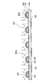
図1は本発明の第1実施例による面光源装置の斜視図であり、図2は図1のA1−A2に沿って切断した断面図である。
Hereinafter, preferred embodiments of the present invention will be described in detail with reference to the accompanying drawings.
<Surface light source device>
(Example 1)
FIG. 1 is a perspective view of a surface light source device according to a first embodiment of the present invention, and FIG. 2 is a cross-sectional view taken along line A 1 -A 2 of FIG.
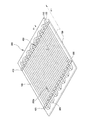
図1及び図2を参照すると、面光源装置500は、基板100、発光本体200、外部光反射部材300、及び光発生装置400を含む。
基板100は、光が透過される透明な基板、例えば、ガラス基板が用いられる。基板100は、互いに向かい合う第1面110、第2面120、及び第1面110と第2面120を連結する側面130で構成される。本実施例において、基板100は、1個の第1面110、1個の第2面120、及び4個の側面130を有する直六面体プレート形状を有する。
Referring to FIGS. 1 and 2, the surface
As the
発光本体200は、基板100の第1面110に蛇行形状で配置される。発光本体200は、縦断面が半円アーチ形状、三角形形状、四角形形状、又は多角形形状を含むことができる。本実施例において、発光本体200の縦断面は半円アーチ形状を有し、光が透過される透明な物質、例えば、ガラスで製作される。
The
発光本体200により基板100の第1面110には、蛇行形状を有する蛇行通路200aが形成され、第1面110に形成された蛇行通路200aは互いに平行し、蛇行通路200aは互いに所定間隔で離隔され配置される。
The
発光本体200及び基板100は、ガラスを含む接着物質等により互いに接着されることができる。発光本体200及び基板100は密封部材、例えば、鉛ガラス等が配置され、密封部材により発光本体200及び基板100は互いにアセンブリされる。
The
光発生装置400は、発光本体200の内部から内部光200bを発生させる。内部光を発生させるために、光発生装置400は、第1電極410、第2電極420、作動ガス430、及び蛍光層440を含む。
The
本実施例において、第1電極410及び第2電極420は、発光本体200の外側面に配置される。第1電極410及び第2電極420は、基板100上に互いに所定間隔で離隔し配置され、蛇行形状で配置された発光本体200を横切って配置される。
In the present embodiment, the
これと異なり、第1電極410及び第2電極420は、発光本体200の内部に配置されることができ、第1電極410及び第2電極420は基板100の第2面120に形成されても良い。
Unlike this, the
第1電極410には第1駆動電圧が印加され、第2電極420には第2駆動電圧が印加される。この際、第1駆動電圧及び第2駆動電圧は、発光本体200の内部で放電が発生するのに充分な電圧差を有する。
A first driving voltage is applied to the
第1電極410及び第2電極420は、発光本体200の外側面に帯形状で形成されることが好ましい。この際、第1電極410及び第2電極420は、液体状態の導電物質を発光本体200に噴射して形成することができる。
The
これと異なり、第1電極410及び第2電極420は、導電性テープ等を用いたり、金属物質をスパッタリング等の方法により形成することができる。
作動ガス430は、発光本体200の内部に配置される。作動ガス430は、水銀、ネオン、アルゴン、キセノン、クリプトン等を含む。作動ガス430は、発光本体200の内部から発生された放電により紫外線等の非可視光線を発生する。
Unlike this, the
The working
蛍光層440は、発光本体200の内壁及び基板100の第1面110のうち、発光本体200により囲まれた位置に、厚さが薄い薄膜形態で配置される。蛍光層440は、作動ガス430及び第1及び第2電極410、420により発生した放電により発生された非可視光線を可視光線に変更させる。
The
一方、基板100及び基板100上に形成された蛍光層420の間には、内部光反射部材450が配置される。内部光反射部材450は、光反射率が高い金属物質を含む薄膜形状を有する。内部光反射部材450は、発光本体200の内部から発生した可視光線又は紫外線のうち、基板100に向かう可視光線又は紫外線を発光本体200に向かって反射させて、発光本体200から出射される可視光線の光量を大きく増加させる。
Meanwhile, an internal
このような構成を有する面光源装置500は、発光本体200の間で輝度均一性が劣化するので、面光源装置500の外部から見た時、輝線が発生する虞がある。
本実施例において、面光源装置500の輝度均一性をより向上させるために、蛇行形状を有する発光本体200の間に対応する基板100には、外部光反射部材300が配置される。
In the surface
In the present embodiment, in order to further improve the luminance uniformity of the surface
本実施例において、外部光反射部材300は、基板100の第1面110に薄い厚さで形成された薄膜を含む。外部光反射部材300から反射される外部光300aは、発光本体200に向かう方向を有する光である。従って、外部光300aは、太陽光、照明器具から発生した光又は面光源装置500の内部から発生され出射された後、面光源装置500に向かって反射された光等を含む。
In this embodiment, the external
外部光反射部材300は、発光本体200に向かって入射された外部光300aを反射して、その結果、光の利用効率及び輝度均一性は大きく向上される。
(実施例2)
図3は、本発明の第2実施例による面光源装置を示す断面図である。本発明の第2実施例による面光源装置は、実施例1の発光本体を除くと、実施例1の面光源装置と同じである。従って、同じ部材には実施例1と同じ参照符号を付与し、その重複説明は省略する。
The external
(Example 2)
FIG. 3 is a cross-sectional view illustrating a surface light source device according to a second embodiment of the present invention. The surface light source device according to the second embodiment of the present invention is the same as the surface light source device according to the first embodiment except for the light emitting main body according to the first embodiment. Therefore, the same reference numerals as those in the first embodiment are given to the same members, and redundant description thereof is omitted.
図3を参照すると、発光本体250は、複数個が基板100の第1面110に配置される。この際、各発光本体250は直線形状を有し、各発光本体250は第1面110に平行に並列配置される。この際、各発光本体250は、互いに一定間隔で離隔され、各発光本体250の間には外部光反射部材300が配置される。
Referring to FIG. 3, a plurality of light emitting bodies 250 are disposed on the
各発光本体250の内部には、均一な圧力で作動ガス430が配置され、作動ガス430はゲッター(getter)等により供給される。
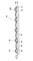
(実施例3)
図4は、本発明の第3実施例による面光源装置を示す断面図である。本発明の第3実施例による面光源装置は、実施例1の外部光反射部材の構造を除くと、実施例1の面光源装置と同じである。従って、同じ部材には実施例1と同じ参照符号を付与し、その重複説明は省略する。
A working
(Example 3)
FIG. 4 is a cross-sectional view illustrating a surface light source device according to a third embodiment of the present invention. The surface light source device according to the third embodiment of the present invention is the same as the surface light source device according to the first embodiment except for the structure of the external light reflecting member according to the first embodiment. Therefore, the same reference numerals as those in the first embodiment are given to the same members, and redundant description thereof is omitted.
図4を参照すると、外部光反射部材310は、基板100の第1面110と向かい合う第2面120に形成される。基板100の第2面120に外部光反射部材310を形成する場合、外部光反射部材310は、基板100の第2面120のうち、発光本体200の間に配置される。
Referring to FIG. 4, the external
本実施例において、外部光反射部材310は、平坦な基板100の第2面120上に形成されるので、液体状態の金属をプリンティング方式で形成するか、薄い薄膜形態のテープを付着して形成することができる。
In this embodiment, since the external
本実施例によると、外部光反射部材310をより容易に基板100上に形成することができる長所を有する。
(実施例4)
図5は、本発明の第4実施例による面光源装置を示す断面図である。本発明の第4実施例による面光源装置は、実施例1の外部光反射部材の構造を除くと、実施例1の面光源装置と同じである。従って、同じ部材には実施例1と同じ参照符号を付与し、その重複説明は省略する。
According to the present embodiment, the external
Example 4
FIG. 5 is a sectional view showing a surface light source device according to a fourth embodiment of the present invention. The surface light source device according to the fourth embodiment of the present invention is the same as the surface light source device of
図5を参照すると、外部光反射部材320は、基板100の第1面110又は第2面120に形成されることができる。本実施例において、外部光反射部材320は第1面110に形成される。又、外部光反射部材320は発光本体200の間に形成される。外部光反射部材320は薄膜形態を有し、半球形状を有する複数個の凸凹322を含む。
Referring to FIG. 5, the external
外部光反射部材320上に複数個の凸凹322を形成するために、基板100の第1面110のうち、発光本体200の間には複数個の突出部が形成される。突出部により外部光反射部材320の上面には、凸凹322が形成される。
In order to form a plurality of
この際、外部光反射部材320は、外部光300aを反射及び外部光300aを凸凹322により散乱させて、面光源装置500から発生した光の輝度分布をより向上させることができる。
(実施例5)
図6は、本発明の第5実施例による面光源装置を示す断面図である。本発明の第5実施例による面光源装置は、実施例1の外部光反射部材の構造を除くと、実施例1の面光源装置と同じである。従って、同じ部材には実施例1と同じ参照符号を付与し、その重複説明は省略する。
At this time, the external
(Example 5)
FIG. 6 is a sectional view showing a surface light source device according to a fifth embodiment of the present invention. The surface light source device according to the fifth embodiment of the present invention is the same as the surface light source device of the first embodiment except for the structure of the external light reflecting member of the first embodiment. Therefore, the same reference numerals as those in the first embodiment are given to the same members, and redundant description thereof is omitted.
図6を参照すると、外部光反射部材330は、基板100の第1面110又は第2面120上に配置され、外部光反射部材330は光をより効率的に拡散又は散乱させるための光拡散パターン332を更に含む。
Referring to FIG. 6, the external
本実施例において、外部光反射部材330に形成された光拡散パターン332は、外部光反射部材330と接する基板100の第1面110又は第2面120上に形成された複数個の反射ドットである。基板100の第1面110又は第2面120に複数個が形成された外部光反射部材330は、外部光300aを反射及び散乱させて面光源装置500の光効率を増加及び光の輝度分布を大きく向上させる。
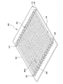
(実施例6)
図7は本発明の第6実施例による面光源装置を示す斜視図であり、図8は図7のB1−B2に沿って切断した断面図である。本発明の第6実施例による面光源装置は、実施例1の外部光反射部材の配置を除くと、実施例1の面光源装置と同じである。従って、同じ部材には、実施例1と同じ参照符号を付与し、その重複説明は省略する。
In this embodiment, the
(Example 6)
FIG. 7 is a perspective view showing a surface light source device according to a sixth embodiment of the present invention, and FIG. 8 is a cross-sectional view taken along B 1 -B 2 of FIG. The surface light source device according to the sixth embodiment of the present invention is the same as the surface light source device of the first embodiment except for the arrangement of the external light reflecting member of the first embodiment. Therefore, the same reference numerals as those in the first embodiment are given to the same members, and a duplicate description thereof is omitted.
図7及び図8を参照すると、面光源装置500は反射本体600を更に含む。
反射本体600は、基板100の第1面110上に配置される。又、反射本体600は蛇行形状で配置された発光本体200の間に配置される。反射本体600は、発光本体200と同じ材質、例えば、ガラス等で製作される。
Referring to FIGS. 7 and 8, the surface
The
反射本体600の縦断面は、半円アーチ形状で製作されることができる。このとき、反射本体600及び基板100の第1面110が形成する第2高さH2は、発光本体200及び基板100の第1面110が形成する第1高さH1以下で形成される。
The longitudinal section of the
反射本体600には外部光反射部材300が選択的に配置される。外部光反射部材300は反射本体600の外側面に配置されたり、反射本体600の内側面に配置されることが好ましい。好ましく、外部光反射部材300は、液体状態の反射物質を反射本体600の外側面又は内側面に塗布して形成することができる。
An external
本実施例において、外部光反射部材300は反射本体600の外側面に形成される。反射本体600の外側面に配置された外部光反射部材300は、外部光を反射させて光の利用効率を増加させ、光の輝度均一性を向上させる。
(実施例7)
図9は、本発明の第7実施例による面光源装置を示す斜視図である。本発明の第7実施例による面光源装置は、実施例6の反射本体の構造を除くと、実施例6の面光源装置と同じである。従って、同じ部材には実施例6と同じ参照符号を付与し、その重複説明は省略する。
In this embodiment, the external
(Example 7)
FIG. 9 is a perspective view showing a surface light source device according to a seventh embodiment of the present invention. The surface light source device according to the seventh embodiment of the present invention is the same as the surface light source device according to the sixth embodiment except for the structure of the reflecting main body according to the sixth embodiment. Therefore, the same reference numerals as those in the sixth embodiment are given to the same members, and a duplicate description thereof is omitted.
図9を参照すると、面光源装置500は反射本体610を更に含む。
反射本体610は、蛇行形状で配置された発光本体200の間に配置される。反射本体610は、発光本体200と同じ材質、例えば、ガラス等で製作され、反射本体610の縦断面は三角形形状又は梯形形状を有する。本実施例において、反射本体610の縦断面は三角形形状を有する。
Referring to FIG. 9, the surface
The
このとき、反射本体610及び基板100の第1面110が形成する第2高さH2は、発光本体610及び基板100の第1面110が形成する第1高さH1以下で形成される。
At this time, the second height H2 formed by the reflective
反射本体610には外部光反射部材300が配置される。外部光反射部材300は、好ましく反射本体610の外側面に配置されたり、反射本体610の内側面に配置されることができる。これと異なり、外部光反射部材300は反射本体610と向かい合う基板100の第1面110上に形成されることができる。本実施例において、外部光反射部材300は好ましく反射本体610の外側面に配置される。好ましく、外部光反射部材300は、液体状態の反射物質を反射本体610の外側面又は内側面に塗布して形成することができる。
(実施例8)
図10は、本発明の第8実施例による面光源装置を示す斜視図である。本発明の第8実施例による面光源装置は、実施例1の外部光反射部材の上面に支持部材が設けられた構造を除くと、実施例1の面光源装置と同じである。従って、同じ部材には実施例1と同じ参照符号を付与し、その重複説明は省略する。
An external
(Example 8)
FIG. 10 is a perspective view showing a surface light source device according to an eighth embodiment of the present invention. The surface light source device according to the eighth embodiment of the present invention is the same as the surface light source device according to the first embodiment except for the structure in which the support member is provided on the upper surface of the external light reflecting member according to the first embodiment. Therefore, the same reference numerals as those in the first embodiment are given to the same members, and the duplicate description thereof is omitted.
図10を参照すると、外部光反射部材300の上面には、所定間隔で支持部材360が配置される。本実施例において、支持部材360は円錐形状を有し、支持部材360の表面には外部光反射部材300を形成する反射物質と同じ反射物質がコーティングされている。
Referring to FIG. 10,
本実施例において、支持部材360は接着剤又は両面接着テープ等により外部光反射部材300の上面に結合される。
支持部材360は、面光源装置500の上面に配置される光学部材、例えば、拡散板及び表示パネルの垂れを防止する。
<表示装置>
図11は、本発明の表示装置の一例を示す部分切開分解斜視図である。この表示装置の面光源装置は、実施例1の面光源装置と同じである。従って、同じ部材には実施例1と同じ参照符号を付与し、その重複説明は省略する。
In this embodiment, the
The
<Display device>
FIG. 11 is a partially cutaway exploded perspective view showing an example of the display device of the present invention. The surface light source device of this display device is the same as the surface light source device of the first embodiment. Therefore, the same reference numerals as those in the first embodiment are given to the same members, and redundant description thereof is omitted.
図11を参照すると、液晶表示装置1000は、収納容器700、面光源装置500、液晶表示パネル800、及びシャーシ900を含む。
収納容器700は、底面710及び底面710のエッジ部に収納空間を形成するために配置された複数個の側壁720、放電電圧印加モジュール732及びインバータ740で構成される。収納容器700の面光源装置500及び液晶表示パネル800が左右で動かないように固定させる。
Referring to FIG. 11, the liquid
The
底面710は、面光源装置500が装着されるのに充分な底面積及び面光源装置500と同じ形状を有する。本実施例において、底面710は面光源装置500と同じ形状を有する直六面体プレート形状を有する。
The bottom surface 710 has a bottom area sufficient for mounting the surface
側壁720は、面光源装置500が外部に離脱しないように底面710から延長又は配置される。
放電電圧印加モジュール732は、面光源装置500の第1及び第2電極410、420に第1駆動電圧及び第2駆動電圧を印加する。
The
The discharge voltage application module 732 applies a first drive voltage and a second drive voltage to the first and
インバータ740は、放電電圧印加モジュール732に第1及び第2駆動電圧を印加する。インバータ740及び放電電圧印加モジュール732は、電源印加線742により連結される。
The
液晶表示パネル800は、面光源装置500から発生した光を情報が含まれたイメージ光に変換する。これを具現するために、液晶表示パネル800はTFT基板810、液晶820、カラーフィルター基板830、及び駆動モジュール840を含む。
The liquid
TFT基板810は、マトリックス形態で配置された画素電極、各画素電極に駆動電圧を印加する薄膜トランジスタ、ゲートライン、及びデータラインを含む。
カラーフィルター基板830は、TFT基板810に形成された画素電極と向かい合うように配置されたカラーフィルター、カラーフィルターの上面に形成された共通電極を含む。
The
The
液晶820は、TFT基板810とカラーフィルター基板830との間に配置される。
一方、液晶表示パネル800のカラーフィルター基板830のエッジ部はシャーシ900により囲まれ、シャーシ900の一部は収納容器700の側壁720に形成されたフックと結合される。シャーシ900は、外部衝撃から脆性が弱い液晶表示パネル800の割れを防止及び液晶表示パネル800が収納容器700から離脱することを防止する。説明されない参照符号850は、面光源装置500から出射された光を拡散させる光拡散部材である。
The
Meanwhile, the edge portion of the
以上で説明したように、面光源装置の構造を変更して、面光源装置から発生する光の利用効率及び面光源装置から発生した光の輝度均一性を向上させ、面光源装置を用いた表示装置から発生した画像の表示品質を向上させる効果を有する。 As described above, the structure of the surface light source device is changed to improve the use efficiency of light generated from the surface light source device and the luminance uniformity of light generated from the surface light source device, and display using the surface light source device This has the effect of improving the display quality of images generated from the apparatus.
以上、本発明の実施例によって詳細に説明したが、本発明はこれに限定されず、本発明が属する技術分野において通常の知識を有するものであれば本発明の思想と精神を離れることなく、本発明を修正または変更できる。 As described above, the embodiments of the present invention have been described in detail. However, the present invention is not limited to the embodiments, and as long as it has ordinary knowledge in the technical field to which the present invention belongs, without departing from the spirit and spirit of the present invention, The present invention can be modified or changed.
100 基板
110 第1面
120 第2面
130 側面
200、250 発光本体
200a 蛇行通路
200b 内部光
300、310、320、330 外部光反射部材
300a 外部光
322 凸凹
332 光拡散パターン
360 支持部材
400 光発生装置
410 第1電極
420 第2電極
430 作動ガス
440 蛍光層
450 内部光反射部材
500 面光源装置
600、610 反射本体
700 収納容器
710 底面
720 側壁
732 放電電圧印加モジュール
740 インバータ
742 電源印加線
800 液晶表示パネル
810 TFT基板
820 液晶
830 カラーフィルター基板
840 駆動モジュール
900 シャーシ
1000 液晶表示装置
100
Claims (22)
前記基板の第1面に互いに離隔された放電空間を形成するために、互いに平行に配置された少なくとも2つの発光本体と、
前記発光本体の内部で内部光を発生させるための光発光装置と、
外部光を反射させるために、前記基板のうち、前記放電空間の間に形成された外部光反射部材と、
を含むことを特徴とする面光源装置。 A substrate having a plate shape;
At least two light emitting bodies disposed parallel to each other to form discharge spaces spaced apart from each other on the first surface of the substrate;
A light emitting device for generating internal light inside the light emitting body;
In order to reflect external light, among the substrates, an external light reflecting member formed between the discharge spaces;
A surface light source device comprising:
前記発光本体の内部で放電を発生させるために、前記発光本体に配置された第1及び第2電極と、
前記放電により非可視光源を発生させる作動ガスと、
前記発光本体及び前記発光本体と対応する前記基板に配置され、前記非可視光線を可視光線に変更する蛍光層と、
を含むことを特徴とする、請求項1に記載の面光源装置。 The light generator is
A first electrode and a second electrode disposed on the light emitting body to generate a discharge inside the light emitting body;
A working gas that generates an invisible light source by the discharge;
A fluorescent layer disposed on the substrate corresponding to the light emitting body and the light emitting body, and changing the invisible light to visible light;
The surface light source device according to claim 1, comprising:
前記外部光及び内部光を情報が含まれたイメージ光に変更させる表示パネルと、
を含むことを特徴とする表示装置。 A plate-shaped substrate in which light-emitting regions and non-light-emitting regions are alternately formed; a light-emitting body disposed on the substrate along the light-emitting region; and a light-reflecting body disposed in the non-light-emitting region and reflecting external light And a surface light source device having a light generator for generating internal light from the light emitting body,
A display panel for changing the external light and the internal light into image light including information;
A display device comprising:
The display device according to claim 19, wherein the optical member is a light diffusion member that diffuses the external light and internal light.
Applications Claiming Priority (1)
| Application Number | Priority Date | Filing Date | Title |
|---|---|---|---|
| KR1020040010929A KR20050082487A (en) | 2004-02-19 | 2004-02-19 | Surface light source device and display device having the same |
Publications (2)
| Publication Number | Publication Date |
|---|---|
| JP2005235773A true JP2005235773A (en) | 2005-09-02 |
| JP2005235773A5 JP2005235773A5 (en) | 2007-06-21 |
Family
ID=34858741
Family Applications (1)
| Application Number | Title | Priority Date | Filing Date |
|---|---|---|---|
| JP2005042893A Withdrawn JP2005235773A (en) | 2004-02-19 | 2005-02-18 | Surface light source device and display device having the same |
Country Status (5)
| Country | Link |
|---|---|
| US (1) | US20050184951A1 (en) |
| JP (1) | JP2005235773A (en) |
| KR (1) | KR20050082487A (en) |
| CN (1) | CN1658042A (en) |
| TW (1) | TW200528874A (en) |
Families Citing this family (11)
| Publication number | Priority date | Publication date | Assignee | Title |
|---|---|---|---|---|
| KR100691179B1 (en) * | 2005-06-01 | 2007-03-09 | 삼성전기주식회사 | Side Emitting LED Package and Method of Manufacturing The Same |
| KR100736778B1 (en) * | 2005-09-05 | 2007-07-09 | 미래산업 주식회사 | Structure of electrode in flat luminescence lamp |
| KR100698513B1 (en) * | 2006-01-27 | 2007-03-21 | 금호전기주식회사 | Flat Fluorescent Lamp |
| JP5453105B2 (en) * | 2006-12-22 | 2014-03-26 | クナノ アーベー | Nanostructured LEDs and devices |
| US8349116B1 (en) | 2011-11-18 | 2013-01-08 | LuxVue Technology Corporation | Micro device transfer head heater assembly and method of transferring a micro device |
| US8794501B2 (en) * | 2011-11-18 | 2014-08-05 | LuxVue Technology Corporation | Method of transferring a light emitting diode |
| US9620478B2 (en) | 2011-11-18 | 2017-04-11 | Apple Inc. | Method of fabricating a micro device transfer head |
| US8573469B2 (en) | 2011-11-18 | 2013-11-05 | LuxVue Technology Corporation | Method of forming a micro LED structure and array of micro LED structures with an electrically insulating layer |
| US9903540B2 (en) * | 2014-02-06 | 2018-02-27 | Appalachian Lighting Systems, Inc. | LED light emitting apparatus having both reflected and diffused subassemblies |
| CN104021732B (en) * | 2014-05-22 | 2017-01-18 | 京东方科技集团股份有限公司 | Display device |
| CN113093433A (en) * | 2021-04-25 | 2021-07-09 | 业成科技(成都)有限公司 | Light source assembly, preparation method thereof, backlight module and display device |
Family Cites Families (11)
| Publication number | Priority date | Publication date | Assignee | Title |
|---|---|---|---|---|
| US5220249A (en) * | 1990-10-08 | 1993-06-15 | Nec Corporation | Flat type fluorescent lamp and method of lighting |
| US5479069A (en) * | 1994-02-18 | 1995-12-26 | Winsor Corporation | Planar fluorescent lamp with metal body and serpentine channel |
| US6655810B2 (en) * | 2000-06-21 | 2003-12-02 | Fujitsu Display Technologies Corporation | Lighting unit |
| JP3850241B2 (en) * | 2001-07-19 | 2006-11-29 | シャープ株式会社 | LIGHTING DEVICE AND LIQUID CRYSTAL DISPLAY DEVICE USING THE SAME |
| JP3620840B2 (en) * | 2002-07-17 | 2005-02-16 | シャープ株式会社 | Liquid crystal display |
| TWI252348B (en) * | 2002-10-21 | 2006-04-01 | Toppoly Optoelectronics Corp | Back light module |
| TW584772B (en) * | 2002-12-17 | 2004-04-21 | Ind Tech Res Inst | Straight-down backlight module |
| US6913378B2 (en) * | 2002-12-27 | 2005-07-05 | Quanta Display Incorporation | Direct-lighting type back light unit |
| US7052152B2 (en) * | 2003-10-03 | 2006-05-30 | Philips Lumileds Lighting Company, Llc | LCD backlight using two-dimensional array LEDs |
| KR100565743B1 (en) * | 2003-10-21 | 2006-03-29 | 엘지.필립스 엘시디 주식회사 | Back light unit |
| TWI280445B (en) * | 2003-12-12 | 2007-05-01 | Ind Tech Res Inst | Light guide apparatus for enhancing light source utilization efficiency |
-
2004
- 2004-02-19 KR KR1020040010929A patent/KR20050082487A/en not_active Application Discontinuation
-
2005
- 2005-01-13 TW TW094100981A patent/TW200528874A/en unknown
- 2005-01-19 US US11/038,896 patent/US20050184951A1/en not_active Abandoned
- 2005-02-08 CN CN2005100516181A patent/CN1658042A/en active Pending
- 2005-02-18 JP JP2005042893A patent/JP2005235773A/en not_active Withdrawn
Also Published As
| Publication number | Publication date |
|---|---|
| CN1658042A (en) | 2005-08-24 |
| US20050184951A1 (en) | 2005-08-25 |
| KR20050082487A (en) | 2005-08-24 |
| TW200528874A (en) | 2005-09-01 |
Similar Documents
| Publication | Publication Date | Title |
|---|---|---|
| JP2005235773A (en) | Surface light source device and display device having the same | |
| KR101508010B1 (en) | System for improved backlight illumination uniformity | |
| JP2006054177A (en) | Backlight assembly, and liquid crystal display device having the same | |
| KR20060023452A (en) | Prism sheet, backlight assembly and liquid crystal display apparatus having the same | |
| JP2006196456A (en) | Backlight assembly and display device provided with same | |
| JP2005025183A (en) | Diffusively reflective member, method of manufacturing the same, and apparatus using the same | |
| JP2005190991A (en) | Lighting system and display device equipped with the same | |
| KR101274687B1 (en) | back light unit and liquid crystal display device using the same | |
| KR100936364B1 (en) | Liquid crystal display module | |
| JP4017039B2 (en) | LIGHTING DEVICE AND DISPLAY DEVICE HAVING THE SAME | |
| KR101341778B1 (en) | Back light unit and liquid crystal display device using the same | |
| JP2007011374A (en) | Back light and liquid crystal display device | |
| KR20050032178A (en) | Surface light source device and liquid crystal display device using the same | |
| US8330896B2 (en) | Liquid crystal display device | |
| JP2005056829A (en) | Surface light source device, and liquid crystal display equipped with the same | |
| KR20060028895A (en) | Backlight unit | |
| KR101308446B1 (en) | Back light unit and liquid crystal display device using the same | |
| KR20070048222A (en) | Illumination system for illuminating display devices and display device comprising such an illumination system | |
| KR100610615B1 (en) | Optical Sheet and Back Light Unit Using the same | |
| KR100610614B1 (en) | Optical Sheet And Back Light Unit Using The Same | |
| JP2005142162A (en) | Surface light source device and display device having the same | |
| KR20130020302A (en) | Backlight unit and display apparatus using the same | |
| JP2008078135A (en) | Surface light source device, drive method thereof, and backlight unit having surface light source device | |
| KR20040029231A (en) | Fluorescent Lamp And Baklight Device With The Same | |
| JP2007027129A (en) | Surface light source device and backlight device having above |
Legal Events
| Date | Code | Title | Description |
|---|---|---|---|
| A521 | Request for written amendment filed |
Free format text: JAPANESE INTERMEDIATE CODE: A523 Effective date: 20070509 |
|
| A621 | Written request for application examination |
Free format text: JAPANESE INTERMEDIATE CODE: A621 Effective date: 20070509 |
|
| A761 | Written withdrawal of application |
Free format text: JAPANESE INTERMEDIATE CODE: A761 Effective date: 20071012 |