JP2005233757A - Method and device for inspecting hole pattern - Google Patents
Method and device for inspecting hole pattern Download PDFInfo
- Publication number
- JP2005233757A JP2005233757A JP2004042919A JP2004042919A JP2005233757A JP 2005233757 A JP2005233757 A JP 2005233757A JP 2004042919 A JP2004042919 A JP 2004042919A JP 2004042919 A JP2004042919 A JP 2004042919A JP 2005233757 A JP2005233757 A JP 2005233757A
- Authority
- JP
- Japan
- Prior art keywords
- hole pattern
- intensity
- rate
- change
- value
- Prior art date
- Legal status (The legal status is an assumption and is not a legal conclusion. Google has not performed a legal analysis and makes no representation as to the accuracy of the status listed.)
- Pending
Links
Images


Abstract
Description
本発明は、ホールパターン検査方法及びホールパターン検査装置に関し、より詳細には、半導体デバイスなどの製造に際して2次電子などを用いて微細なホール(穴)パターンの開孔状態を確実且つ容易に識別できるホールパターン検査方法及びホールパターン検査装置に関する。 The present invention relates to a hole pattern inspection method and a hole pattern inspection apparatus, and more particularly, to reliably and easily identify the opening state of a fine hole (hole) pattern using secondary electrons or the like when manufacturing a semiconductor device or the like. The present invention relates to a hole pattern inspection method and a hole pattern inspection apparatus.
半導体集積回路装置などの半導体デバイスは、幾重にも重なった層状の配線層を有し、各々の配線層間には絶縁層が設けられている。この半導体デバイスを電気回路として成り立たせるためには、絶縁層の所望箇所に「コンタクトホール(contact hole)」あるいは「ビアホール(via hole)」などと呼ばれる孔を形成し、導電性材料を充填して各配線層間を電気的に接続する必要がある。 A semiconductor device such as a semiconductor integrated circuit device has layered wiring layers that are stacked one on another, and an insulating layer is provided between each wiring layer. In order to establish this semiconductor device as an electric circuit, holes called “contact holes” or “via holes” are formed in desired portions of the insulating layer and filled with a conductive material. It is necessary to electrically connect each wiring layer.
図6は、コンタクトホールの形成工程を表す工程断面図である。
半導体基板や下層配線層からなる下地500の上には、SiO2等の被エッチング膜501が設けられている。まず、この被エッチング膜501の上に、リソグラフィ工程によってマスク502を形成する。具体的には、「フォトレジスト」などと呼ばれる感光性の高分子膜を形成し、アルカリ現像を施して微細なホールパターンを形成する(図6(a))。
次に、エッチング工程によって、マスク502をエッチング阻止部として機能させ、被エッチング膜501にマスクパターンの転写像であるホールパターンを形成する(図6(b))。
続いて、このホールパターンに導電性の材料503を埋め込んで、接続部を形成する(図6(c))。
FIG. 6 is a process sectional view showing a contact hole forming process.
An
Next, the etching process causes the mask 502 to function as an etching blocking portion, and a hole pattern, which is a transfer image of the mask pattern, is formed on the etching target film 501 (FIG. 6B).
Subsequently, a
以上説明した工程からも分かるように、マスク502や被エッチング膜501に形成するホールパターンは、厳密に開孔していることが必要である。このようなホールパターンの開孔状態の検査は、走査型電子顕微鏡(Scanning Electron Microscope:SEM)で行うことができる。すなわち、ホールパターンが所望の開孔状態を有するか否かは、SEMによる寸法の測定値が特異的でないこと、および2次電子のコントラスト像におけるホール底部の見え方が異常でないこと等から判断していた。このうち、寸法の測定値が特異的でないかの判断は、基準値との比較によって一意的に決めることができるため、自動化は容易である。しかし、ホール底部の見え方が異常でないかの判断は、人手による作業が必要となり、SEM検査の自動化に対する大きな障害となっていた。
As can be seen from the above-described steps, the hole pattern formed in the mask 502 or the
このように、従来の検査方法においては、ホールパターンが開孔しているかどうかの判断に人手による作業が必要となり、大きな労力を要していた。さらに、近年ではホールパターンの微細化に伴って、ホール底部から得られる2次電子の情報量が大幅に低減し、ホール底部のSEM像の見え方が不鮮明となり、人手による判断作業も困難になってきた。 As described above, in the conventional inspection method, it is necessary to perform a manual operation to determine whether or not the hole pattern is open. Furthermore, in recent years, with the miniaturization of the hole pattern, the amount of secondary electron information obtained from the bottom of the hole has been greatly reduced, the SEM image of the bottom of the hole has become unclear, and it has become difficult to make manual judgments. I came.
本発明はかかる課題の認識に基づいてなされたものであり、その目的は、SEMなどによる簡便化されたホールパターン検査方法を提供することにある。また、この検査方法を用いることにより、自動化をされたホールパターン検査装置を提供することも目的とする。 The present invention has been made based on the recognition of such a problem, and an object thereof is to provide a simplified hole pattern inspection method using SEM or the like. It is another object of the present invention to provide an automated hole pattern inspection apparatus by using this inspection method.
図7は、SEMにおけるパターン寸法の決定方法を示した模式図である。 FIG. 7 is a schematic diagram showing a method for determining a pattern dimension in the SEM.
SEMを用いた場合、パターンの形状に依存して2次電子の強度が変動する現象を利用し、2次電子のコントラスト情報を用いることによってパターン寸法を決定できる。図7(a)はホールパターン601の断面形状、図7(b)はホールパターン601の2次電子のコントラスト波形602をそれぞれ表す。
When the SEM is used, the pattern dimension can be determined by using a phenomenon in which the intensity of the secondary electrons varies depending on the shape of the pattern and using the contrast information of the secondary electrons. FIG. 7A shows a cross-sectional shape of the
ホールパターン寸法は、ある特定の2次電子強度(以下、「しきい値」と称する)におけるエッジ間の距離、すなわち、コントラスト波形602と、しきい値に対応する直線603と、が交差する線分604の長さによって求められる。2次電子強度のしきい値としては、2次電子強度の最大値と最小値の50パーセント程度の値を用いることができる。これは、ホールパターン側壁部の側壁の状態をよく表現できることと、安定した測定が行えるからである。
The hole pattern dimension is a distance between edges at a specific secondary electron intensity (hereinafter referred to as “threshold”), that is, a line where a
コントラスト波形602は、ホールパターン上部の開孔端の角部では2次電子が放出されやすく、強度は強くなる。ホールパターン側壁部では、その傾きと深さに応じた強度となり、底部では、その材質と深さに応じた強度を有する。このように、SEM観察で得られる2次電子のコントラスト波形の形状は、ホールパターンの断面形状を強く反映した形となる。従って、このコントラスト波形を用いて、あらゆるしきい値におけるパターン寸法を詳細に調べれば、パターン形状を詳細に把握することが可能となる。
In the
本発明では、あらゆるしきい値におけるパターン寸法を詳細に調べ、所定のしきい値でのホールパターン寸法の変化の割合を知ることで、パターンの断面形状を定量的に評価する検査方法を提供するものである。 The present invention provides an inspection method for quantitatively evaluating the cross-sectional shape of a pattern by examining the pattern dimensions at every threshold in detail and knowing the rate of change in the hole pattern dimension at a predetermined threshold. Is.
すなわち、本発明によれば、
ホールパターンに電子ビームを照射して2次電子信号を得る手順と、
前記2次電子信号の強度が指定強度となる範囲をホールパターンの開孔寸法とし、第1の指定強度から前記第1の指定強度よりも大なる第2の指定強度に至る範囲における前記ホールパターンの前記開孔寸法の寸法曲線を算出する手順と、
前記第1の値と前記第2の値との間の第3の指定強度における前記開孔寸法の寸法曲線の変化の割合を算出する手順と、
前記変化の割合から、前記ホールパターンの形成状態の良否を判定する手順と、
を備えたことを特徴とするホールパターン検査方法が提供される。
That is, according to the present invention,
A procedure for obtaining a secondary electron signal by irradiating an electron beam to a hole pattern;
A range in which the intensity of the secondary electron signal becomes a specified intensity is a hole pattern opening size, and the hole pattern in a range from a first specified intensity to a second specified intensity greater than the first specified intensity. A procedure for calculating a dimension curve of the opening dimension of
Calculating a rate of change of the dimension curve of the opening dimension at a third specified intensity between the first value and the second value;
From the rate of change, a procedure for determining the quality of the hole pattern formation state;
A hole pattern inspection method is provided.
ここで、前記第1の指定強度は、前記2次電子信号の最小値であり、前記第2の指定強度は、前記2次電子信号の最大値であり、前記第3の指定強度は、前記第1及び第2の指定強度の略平均値であるものとすることができる。 Here, the first designated strength is a minimum value of the secondary electron signal, the second designated strength is a maximum value of the secondary electron signal, and the third designated strength is It may be an approximate average value of the first and second designated intensities.
また、前記変化の割合が所定値よりも小なるときに前記ホールパターンの形成状態を良と判定することができる。 In addition, when the rate of change is smaller than a predetermined value, the formation state of the hole pattern can be determined as good.
また、前記第1の指定強度の近傍における前記開孔寸法の寸法曲線の変化の割合を算出する手順と、前記第1の指定強度の近傍における前記変化の割合から、前記ホールパターンの形成状態の良否を判定する手順と、をさらに備えたものとすることができる。 Further, from the procedure for calculating the change rate of the dimension curve of the opening dimension in the vicinity of the first specified strength and the change rate in the vicinity of the first specified strength, the formation state of the hole pattern is determined. And a procedure for determining pass / fail.
またこの場合、前記第1の指定強度の近傍における前記変化の割合が所定値よりも大なるときに前記ホールパターンの形成状態を良と判定することができる。 Further, in this case, when the rate of change in the vicinity of the first designated intensity is greater than a predetermined value, the hole pattern formation state can be determined to be good.
または、本発明によれば、
ホールパターンに電子ビームを照射して2次電子信号を得る手段と、
前記2次電子信号の強度が指定強度となる範囲をホールパターンの開孔寸法とし、第1の指定強度から前記第1の指定強度よりも大なる第2の指定強度に至る範囲における前記ホールパターンの前記開孔寸法の寸法曲線を算出する手段と、
前記第1の値と前記第2の値との間の第3の指定強度における前記開孔寸法の寸法曲線の変化の割合を算出する手段と、
前記変化の割合から、前記ホールパターンの形成状態の良否を判定する手段と、
を備えたことを特徴とするホールパターン検査装置が提供される。
Or according to the invention,
Means for irradiating a hole pattern with an electron beam to obtain a secondary electron signal;
A range in which the intensity of the secondary electron signal becomes a specified intensity is a hole pattern opening size, and the hole pattern in a range from a first specified intensity to a second specified intensity greater than the first specified intensity. Means for calculating a dimensional curve of the opening size of
Means for calculating a rate of change of the dimension curve of the aperture size at a third specified intensity between the first value and the second value;
Means for determining the quality of the formation state of the hole pattern from the rate of change;
A hole pattern inspection apparatus is provided.
ここで、前記第1の指定強度の近傍における前記開孔寸法の寸法曲線の変化の割合を算出する手段と、前記第1の指定強度の近傍における前記変化の割合から、前記ホールパターンの形成状態の良否を判定する手段と、をさらに備えたものとすることができる。 Here, from the means for calculating the rate of change of the dimension curve of the aperture size in the vicinity of the first specified intensity, and the rate of change in the vicinity of the first specified intensity, the formation state of the hole pattern And a means for judging whether the quality is good or bad.
本発明によれば、あらゆるしきい値におけるホールパターン寸法を詳細に調べることでホールパターンの断面形状を定量的に評価することが可能となる。また、このとき、あるしきい値でのホールパターン寸法の変化の割合を用いて、ホールパターン形状の良否を判定できるので、ホールパターンの開孔状態を自動的に識別することができる。 According to the present invention, it is possible to quantitatively evaluate the cross-sectional shape of the hole pattern by examining the hole pattern dimensions at every threshold value in detail. At this time, since the quality of the hole pattern shape can be determined using the rate of change of the hole pattern dimension at a certain threshold value, the hole pattern opening state can be automatically identified.
以下、図面を参照しつつ本発明の実施の形態について説明する。 Hereinafter, embodiments of the present invention will be described with reference to the drawings.
図1は、本発明の実施の形態にかかるホールパターン検査方法を表すフローチャートである。
すなわち、本実施形態においては、まず、ステップS102において、被測定体の2次電子信号波形を取得する。具体的には、例えば、ホールパターンを形成したウェーハをSEMに設置して電子線を照射し、ホールパターンの形状に対応した2次電子の信号波形を取得する。
FIG. 1 is a flowchart showing a hole pattern inspection method according to an embodiment of the present invention.
That is, in this embodiment, first, in step S102, the secondary electron signal waveform of the measurement object is acquired. Specifically, for example, a wafer on which a hole pattern is formed is placed in an SEM and irradiated with an electron beam to acquire a secondary electron signal waveform corresponding to the shape of the hole pattern.
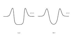
図2は、ホールパターンの断面形状を例示する模式図である。図2(a)はパターン底部の開孔状態が良好なパターン101を、図2(b)はパターン底部の開孔状態が良くないパターン102をそれぞれ表す。ホールパターン101は、側壁が直線状で、側壁と底部との境界形状もシャープである。一方、ホールパターン102は、側壁の直線区間が短く、側壁と底部との境界形状も丸みを帯びている。
FIG. 2 is a schematic view illustrating the cross-sectional shape of the hole pattern. FIG. 2A shows a pattern 101 with a good pattern at the bottom of the pattern, and FIG. 2B shows a
図3は、図2に表したホールパターンの2次電子コントラスト波形を表す模式図である。すなわち、図3(a)は図2(a)のパターン101のコントラスト波形201を、図3(b)は図2(b)のパターン102のコントラスト波形202をそれぞれ表す。コントラスト波形201と202とを比較すると、コントラスト波形202では側壁部の傾きがなだらかであり、側壁部と底部との境界領域の曲半径も大きくなっていることが分かる。
FIG. 3 is a schematic diagram showing a secondary electron contrast waveform of the hole pattern shown in FIG. 3A shows the
再び図1に戻って説明を続けると、次に、ステップS104において、パターン寸法曲線を演算する。すなわち、ステップS102において取得した2次電子信号波形から、それぞれのしきい値におけるホールパターンの開孔寸法を算出する。 Returning to FIG. 1 again, the description will be continued. Next, in step S104, a pattern dimension curve is calculated. That is, the aperture size of the hole pattern at each threshold value is calculated from the secondary electron signal waveform acquired in step S102.
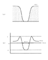
図4は、しきい値を0から100パーセントまで変化させた場合の、コントラスト波形から求めたパターン寸法を示したグラフである。すなわち、同図の横軸はしきい値を表し、縦軸はしきい値50パーセントにおけるパターン寸法を1.0としたときのパターン寸法を表す。ここで、しきい値50パーセントを基準としたのは、この付近において安定したパターン寸法が得られるからである。 FIG. 4 is a graph showing pattern dimensions obtained from the contrast waveform when the threshold value is changed from 0 to 100 percent. That is, the horizontal axis in the figure represents the threshold value, and the vertical axis represents the pattern dimension when the pattern dimension at the threshold of 50% is 1.0. Here, the threshold value of 50% is used as a reference because a stable pattern dimension can be obtained in this vicinity.
図4(a)は図3(a)より求めた寸法曲線301を表し、図4(b)は図3(b)より求めた寸法曲線302を表す。寸法曲線301、および302は、しきい値が50パーセント付近から小さくなるに従い、寸法が直線的に減少し、ある値を境に急激に減少する傾向にある。この急激に寸法が小さくなる点がホールパターンの側壁部と底部との境界領域付近であり、寸法曲線のカーブが底部のパターン形状を反映していることが分かる。
4A shows the
再び図1に戻って説明を続けると、次に、ステップS106において、所定のしきい値における傾きを算出する。すなわち、図4に例示したような寸法曲線において、所定のしきい値における曲線の傾きを算出する。 Returning to FIG. 1 again, the description will be continued. Next, in step S106, an inclination at a predetermined threshold value is calculated. That is, in the dimensional curve illustrated in FIG. 4, the slope of the curve at a predetermined threshold value is calculated.
例えば、図4(a)、(b)において、寸法が直線的に減少する区間のあるしきい値、例えばしきい値50パーセントのときの接線を、それぞれ接線303、304とすると、
(接線303の傾き) < (接線304の傾き)
となる。
For example, in FIGS. 4 (a) and 4 (b), a certain threshold value in a section in which the dimension decreases linearly, for example, tangent lines at a threshold value of 50% are
(Slope of tangent 303) <(Slope of tangent 304)
It becomes.
つまり、しきい値50パーセントの時の傾きは、ホールパターン101のほうがホールパターン102よりも小さい。これは、図2及び図3からも分かるように、ホールパターンの側壁がより急峻に形成されている場合には、寸法曲線における直線部の傾斜が小さくなるからである。
That is, the inclination when the threshold value is 50% is smaller in the hole pattern 101 than in the
従って、この場合には、図1に表したステップS108において、しきい値50パーセントにおける傾きが所定値以下の場合に、ホールパターンの開孔状態は良好であると判定できる。 Therefore, in this case, when the slope at the threshold value of 50% is equal to or smaller than the predetermined value in step S108 shown in FIG. 1, it can be determined that the hole pattern has a good hole state.
一方、寸法が急激に減少する区間のあるしきい値、例えばしきい値5パーセントのときの接線を、それぞれ接線305、306とすると、
(接線305の傾き) > (接線306の傾き)
となる。
On the other hand, when a threshold having a section in which the dimension decreases rapidly, for example, tangents at a threshold of 5% are
(Slope of tangent 305)> (Slope of tangent 306)
It becomes.
つまり、しきい値5パーセントの時の傾きは、ホールパターン101のほうがホールパターン102よりも大きい。これは、図2及び図3からも分かるように、ホールパターンの側壁がより急峻に形成されている場合には、開孔の底部付近における寸法曲線の傾斜が大きくなるからである。
That is, the inclination at the threshold of 5% is larger in the hole pattern 101 than in the
従って、この場合には、図1に表したステップS108において、しきい値5パーセントにおける傾きが所定値以上の場合に、ホールパターンの開孔状態は良好であると判定できる。 Therefore, in this case, when the slope at the threshold value of 5% is equal to or larger than the predetermined value in step S108 shown in FIG. 1, it can be determined that the hole pattern has a good hole state.
すなわち、図2〜3から分かるように、しきい値50パーセント時の接線の傾きが小さく、しきい値5パーセント時の接線の傾きが大きいホールパターン101の方が開孔状態が良いと判断できる。ここでは、ホールパターンの側壁部と底部の境界領域としてしきい値5パーセントを例に示したが、しきい値の最小値に近い値であればよい。 That is, as can be seen from FIGS. 2 to 3, it can be determined that the hole pattern 101 has a smaller tangential slope at the threshold of 50% and a larger tangent slope at the threshold of 5% and has a better opening state. . Here, the threshold value of 5% is shown as an example of the boundary region between the side wall and bottom of the hole pattern, but any value close to the minimum value of the threshold may be used.
本発明者が、多くの開孔状態のパターンにおいて、コントラスト波形より求めた寸法曲線の接線の傾きを調べたところ、開孔状態が良好なパターンにおいては
(接線303の傾き) < 0.2
(接線305の傾き) > 20
という結果が得られた。
The inventor examined the tangential slope of the dimensional curve obtained from the contrast waveform in many patterns of open states.
(Slope of tangent 303) <0.2
(Inclination of tangent 305)> 20
The result was obtained.
つまり、ホールパターンの検査時に、しきい値を最小値から最大値まで変化させて寸法曲線を得、しきい値50パーセント時の接線の傾きを算出し、この値が0.2以上である場合に、開孔状態を「NG」と判定することができる。 In other words, when inspecting the hole pattern, the threshold value is changed from the minimum value to the maximum value to obtain a dimensional curve, and the slope of the tangent line when the threshold value is 50% is calculated, and this value is 0.2 or more In addition, the open state can be determined as “NG”.
同様に、しきい値を最小値から最大値まで変化させて寸法曲線を得、しきい値5パーセント時の接線の傾きを算出し、この値が20以下である場合に、開孔状態を「NG」と判定することができる。 Similarly, the threshold value is changed from the minimum value to the maximum value to obtain a dimensional curve, and the slope of the tangent line at the time of the threshold value of 5% is calculated. NG ".
このように、ホールパターンの開孔状態の良し悪しは、寸法曲線の接線の傾きの大小によって判定できる。 Thus, the quality of the hole pattern open state can be determined by the magnitude of the tangent slope of the dimension curve.
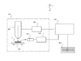
図5は、本発明の実施の形態にかかるホールパターン検査装置の要部構成を例示するブロック図である。
ホールパターン検査装置40は、SEM装置401と、コンピュータ402と、入力部403と、を備える。SEM装置401は、電子光学系404と、被測定体Sを載置するステージ405と、電子光学系処理部406と、2次電子検出器407と、信号処理部408と、より構成される。電子光学系404は、電子ビームを生成して検査対象であるホールパターンが形成された被測定体Sに電子ビームを照射する。2次電子検出器407は、電子ビームの照射により被測定体Sの表面から放出された2次電子を検出する。信号処理部408は、2次電子検出器407により検出された2次電子を変換して2次電子信号としてコンピュータ402に供給する。コンピュータ402は、装置全体を制御する。コンピュータ402は、SEM装置401から供給される、2次電子信号を処理し、上記ホールパターン検査方法で説明した手順により、ホールパターンの形状の良否を判定する。入力部403は、コンピュータ402に接続されており、しきい値データ、接線の傾きのデータを入力が可能である。
FIG. 5 is a block diagram illustrating the main configuration of the hole pattern inspection apparatus according to the embodiment of the invention.
The hole
入力部403によって、ホールパターン検査装置に、例えばしきい値50パーセント時の寸法曲線の接線の傾きが0.2以上である場合に、開孔状態を「NG」と判定する旨を設定することで、これ以降のパターン検査を自動で行うことができる。 The input unit 403 is configured to set in the hole pattern inspection apparatus that, for example, when the tangent slope of the dimensional curve at the threshold value of 50% is 0.2 or more, the hole state is determined as “NG”. Thus, the subsequent pattern inspection can be automatically performed.
以上、具体例を参照しつつ本発明の実施の形態について説明した。しかし、本発明は、これらの具体例に限定されるものではない。 The embodiments of the present invention have been described above with reference to specific examples. However, the present invention is not limited to these specific examples.
例えば、本発明は、コンタクトホールやビアホールの開孔状態を測定するためのみに用いられるものではなく、例えば、キャパシタやゲート構造を得るためのトレンチや、素子間絶縁層を形成するためのトレンチなど、各種の孔の開孔状態の測定に適用して同様の作用効果が得られる。また、その測定装置は、SEMを用いたものには限定されず、被測定体に電子線を照射して2次電子を検出可能としたものであればよい。
半導体集積回路のウェーハ上にレジストを形成した被処理体に電子線描画を行うための電子線描画データの検証にも適用できる。
For example, the present invention is not used only for measuring the opening state of contact holes and via holes. For example, a trench for obtaining a capacitor or a gate structure, a trench for forming an inter-element insulating layer, etc. When applied to the measurement of the open state of various holes, the same effect can be obtained. Further, the measuring apparatus is not limited to the one using the SEM, and may be any apparatus that can detect the secondary electrons by irradiating the measurement object with an electron beam.
The present invention can also be applied to verification of electron beam drawing data for performing electron beam drawing on an object to be processed on which a resist is formed on a semiconductor integrated circuit wafer.
その他、本発明の要素を具備し、当業者が適宜設計変更しうる全てのホールパターン検査方法及びホールパターン検査装置は本発明の範囲に包含される。 In addition, all hole pattern inspection methods and hole pattern inspection apparatuses that include the elements of the present invention and that can be appropriately modified by those skilled in the art are included in the scope of the present invention.
101 、102、601 ホールパターン
40 ホールパターン検査装置
401 SEM装置
402 コンピュータ
403 入力部
404 電子光学系
405 ステージ
406 電子光学系処理部
407 2次電子検出器
408 信号処理部
501 被エッチング膜
502 フォトレジスト
503 導電性材料
101, 102, 601
Claims (7)
前記2次電子信号の強度が指定強度となる範囲をホールパターンの開孔寸法とし、第1の指定強度から前記第1の指定強度よりも大なる第2の指定強度に至る範囲における前記ホールパターンの前記開孔寸法の寸法曲線を算出する手順と、
前記第1の値と前記第2の値との間の第3の指定強度における前記開孔寸法の寸法曲線の変化の割合を算出する手順と、
前記変化の割合から、前記ホールパターンの形成状態の良否を判定する手順と、
を備えたことを特徴とするホールパターン検査方法。 A procedure for obtaining a secondary electron signal by irradiating an electron beam to a hole pattern;
A range in which the intensity of the secondary electron signal becomes a specified intensity is a hole pattern opening size, and the hole pattern in a range from a first specified intensity to a second specified intensity greater than the first specified intensity. A procedure for calculating a dimension curve of the opening dimension of
Calculating a rate of change of the dimension curve of the opening dimension at a third specified intensity between the first value and the second value;
From the rate of change, a procedure for determining the quality of the hole pattern formation state;
A hole pattern inspection method characterized by comprising:
前記第2の指定強度は、前記2次電子信号の最大値であり、
前記第3の指定強度は、前記第1及び第2の指定強度の略平均値であることを特徴とする請求項1記載のホールパターン検査方法。 The first designated intensity is a minimum value of the secondary electron signal;
The second designated intensity is a maximum value of the secondary electron signal;
2. The hole pattern inspection method according to claim 1, wherein the third designated intensity is a substantially average value of the first and second designated intensity.
前記第1の指定強度の近傍における前記変化の割合から、前記ホールパターンの形成状態の良否を判定する手順と、
をさらに備えたことを特徴とする請求項1〜3のいずれか1つに記載のホールパターン検査方法。 Calculating a rate of change of the dimension curve of the aperture size in the vicinity of the first specified strength;
A procedure for determining pass / fail of the formation state of the hole pattern from the rate of change in the vicinity of the first designated intensity;
The hole pattern inspection method according to claim 1, further comprising:
前記2次電子信号の強度が指定強度となる範囲をホールパターンの開孔寸法とし、第1の指定強度から前記第1の指定強度よりも大なる第2の指定強度に至る範囲における前記ホールパターンの前記開孔寸法の寸法曲線を算出する手段と、
前記第1の値と前記第2の値との間の第3の指定強度における前記開孔寸法の寸法曲線の変化の割合を算出する手段と、
前記変化の割合から、前記ホールパターンの形成状態の良否を判定する手段と、
を備えたことを特徴とするホールパターン検査装置。 Means for irradiating a hole pattern with an electron beam to obtain a secondary electron signal;
A range in which the intensity of the secondary electron signal becomes a specified intensity is a hole pattern opening size, and the hole pattern in a range from a first specified intensity to a second specified intensity greater than the first specified intensity. Means for calculating a dimensional curve of the opening size of
Means for calculating a rate of change of the dimension curve of the aperture size at a third specified intensity between the first value and the second value;
Means for determining the quality of the formation state of the hole pattern from the rate of change;
A hole pattern inspection apparatus comprising:
前記第1の指定強度の近傍における前記変化の割合から、前記ホールパターンの形成状態の良否を判定する手段と、
をさらに備えたことを特徴とする請求項6記載のホールパターン検査装置。
Means for calculating a rate of change of a dimension curve of the aperture size in the vicinity of the first designated strength;
Means for determining the quality of the formation state of the hole pattern from the rate of change in the vicinity of the first designated intensity;
The hole pattern inspection apparatus according to claim 6, further comprising:
Priority Applications (1)
| Application Number | Priority Date | Filing Date | Title |
|---|---|---|---|
| JP2004042919A JP2005233757A (en) | 2004-02-19 | 2004-02-19 | Method and device for inspecting hole pattern |
Applications Claiming Priority (1)
| Application Number | Priority Date | Filing Date | Title |
|---|---|---|---|
| JP2004042919A JP2005233757A (en) | 2004-02-19 | 2004-02-19 | Method and device for inspecting hole pattern |
Publications (2)
| Publication Number | Publication Date |
|---|---|
| JP2005233757A true JP2005233757A (en) | 2005-09-02 |
| JP2005233757A5 JP2005233757A5 (en) | 2008-12-18 |
Family
ID=35016879
Family Applications (1)
| Application Number | Title | Priority Date | Filing Date |
|---|---|---|---|
| JP2004042919A Pending JP2005233757A (en) | 2004-02-19 | 2004-02-19 | Method and device for inspecting hole pattern |
Country Status (1)
| Country | Link |
|---|---|
| JP (1) | JP2005233757A (en) |
Cited By (2)
| Publication number | Priority date | Publication date | Assignee | Title |
|---|---|---|---|---|
| WO2007114642A1 (en) * | 2006-04-03 | 2007-10-11 | Cebt Co. Ltd. | Hole inspection apparatus and hole inspection method using the same |
| JP2011192837A (en) * | 2010-03-15 | 2011-09-29 | Toshiba Corp | Evaluating device and evaluating method |
-
2004
- 2004-02-19 JP JP2004042919A patent/JP2005233757A/en active Pending
Cited By (2)
| Publication number | Priority date | Publication date | Assignee | Title |
|---|---|---|---|---|
| WO2007114642A1 (en) * | 2006-04-03 | 2007-10-11 | Cebt Co. Ltd. | Hole inspection apparatus and hole inspection method using the same |
| JP2011192837A (en) * | 2010-03-15 | 2011-09-29 | Toshiba Corp | Evaluating device and evaluating method |
Similar Documents
| Publication | Publication Date | Title |
|---|---|---|
| US6815345B2 (en) | Method for in-line monitoring of via/contact holes etch process based on test structures in semiconductor wafer manufacturing | |
| JP5543984B2 (en) | CD measurement system and method for classifying similar structural elements | |
| KR101013346B1 (en) | Monitoring of contact hole production | |
| JP2005244218A (en) | Board measuring device and board measuring method | |
| JP2007502028A (en) | Contact opening measurement method | |
| US7733502B2 (en) | Roughness evaluation method and system | |
| JP4240066B2 (en) | Etching process monitoring method and etching process control method | |
| JP4991099B2 (en) | Method and system for monitoring an IC process | |
| US6277661B1 (en) | Method for detecting sloped contact holes using a critical-dimension waveform | |
| JP4220335B2 (en) | 3D shape measuring device | |
| JP2005233757A (en) | Method and device for inspecting hole pattern | |
| TWI652446B (en) | Image analysis device and charged particle beam device | |
| KR20050045892A (en) | Method and system for monitoring ic process | |
| JP2007194422A (en) | Test pattern wafer for defect inspecting device, its manufacturing method, and evaluation method of defect inspection apparatus using it | |
| JP5733011B2 (en) | Defect inspection method, semiconductor device manufacturing method, and defect inspection apparatus | |
| Momonoi et al. | CD-SEM metrology of spike detection on sub-40 nm contact holes | |
| JP2005207802A (en) | Resist pattern inspection method, and inspection device therefor | |
| KR20080051554A (en) | Method of evaluating critical dimension for semiconductor device | |
| JP2017102039A (en) | Pattern measurement program, pattern measurement method, and device | |
| KR100816193B1 (en) | Method of examining exposure process for semiconductor device fabrication | |
| KR20240048213A (en) | Overlay measuring methods and system, and method of manufacturing a semiconductor device using the same | |
| JP2007036155A (en) | Evaluation method for failure of opening and manufacturing method for semiconductor | |
| JP2006073701A (en) | Method for monitoring etching process | |
| JP2008020735A (en) | Evaluation method for photomask and method for manufacturing semiconductor device | |
| KR100807044B1 (en) | Method of examining process for semiconductor device fabrication |
Legal Events
| Date | Code | Title | Description |
|---|---|---|---|
| A521 | Written amendment |
Free format text: JAPANESE INTERMEDIATE CODE: A821 Effective date: 20050426 |
|
| A621 | Written request for application examination |
Free format text: JAPANESE INTERMEDIATE CODE: A621 Effective date: 20060815 |
|
| A977 | Report on retrieval |
Free format text: JAPANESE INTERMEDIATE CODE: A971007 Effective date: 20080925 |
|
| A521 | Written amendment |
Free format text: JAPANESE INTERMEDIATE CODE: A523 Effective date: 20081029 |
|
| A131 | Notification of reasons for refusal |
Free format text: JAPANESE INTERMEDIATE CODE: A131 Effective date: 20081121 |
|
| A711 | Notification of change in applicant |
Free format text: JAPANESE INTERMEDIATE CODE: A712 Effective date: 20081126 |
|
| A02 | Decision of refusal |
Free format text: JAPANESE INTERMEDIATE CODE: A02 Effective date: 20090408 |