JP2005208120A - Sample correcting apparatus, sample correction method, and device manufacturing method using the method - Google Patents
Sample correcting apparatus, sample correction method, and device manufacturing method using the method Download PDFInfo
- Publication number
- JP2005208120A JP2005208120A JP2004011787A JP2004011787A JP2005208120A JP 2005208120 A JP2005208120 A JP 2005208120A JP 2004011787 A JP2004011787 A JP 2004011787A JP 2004011787 A JP2004011787 A JP 2004011787A JP 2005208120 A JP2005208120 A JP 2005208120A
- Authority
- JP
- Japan
- Prior art keywords
- sample
- electron beam
- objective lens
- corrected
- electron
- Prior art date
- Legal status (The legal status is an assumption and is not a legal conclusion. Google has not performed a legal analysis and makes no representation as to the accuracy of the status listed.)
- Ceased
Links
Images


Classifications
-
- H—ELECTRICITY
- H01—ELECTRIC ELEMENTS
- H01J—ELECTRIC DISCHARGE TUBES OR DISCHARGE LAMPS
- H01J37/00—Discharge tubes with provision for introducing objects or material to be exposed to the discharge, e.g. for the purpose of examination or processing thereof
- H01J37/02—Details
- H01J37/18—Vacuum locks ; Means for obtaining or maintaining the desired pressure within the vessel
-
- H—ELECTRICITY
- H01—ELECTRIC ELEMENTS
- H01J—ELECTRIC DISCHARGE TUBES OR DISCHARGE LAMPS
- H01J2237/00—Discharge tubes exposing object to beam, e.g. for analysis treatment, etching, imaging
- H01J2237/18—Vacuum control means
- H01J2237/188—Differential pressure
-
- H—ELECTRICITY
- H01—ELECTRIC ELEMENTS
- H01J—ELECTRIC DISCHARGE TUBES OR DISCHARGE LAMPS
- H01J2237/00—Discharge tubes exposing object to beam, e.g. for analysis treatment, etching, imaging
- H01J2237/30—Electron or ion beam tubes for processing objects
- H01J2237/317—Processing objects on a microscale
- H01J2237/3174—Etching microareas
- H01J2237/31742—Etching microareas for repairing masks
- H01J2237/31744—Etching microareas for repairing masks introducing gas in vicinity of workpiece
Abstract
Description
本発明は、0.1μm以下の線幅のデバイス等を製造するマスク等の試料の欠陥を高精度で修正(リペア)する試料修正装置及び試料修正方法に関し、さらにその様な試料修正方法を用いたデバイス製造方法に関する。 The present invention relates to a sample correction apparatus and a sample correction method for correcting (repairing) a defect of a sample such as a mask for manufacturing a device having a line width of 0.1 μm or less with high accuracy, and further uses such a sample correction method. The present invention relates to a device manufacturing method.
従来において、細く絞った電子線をマスク等の試料に照射し、照射点にノズルで反応ガスを吹き付け、試料のエッチングを行う方法は公知である。 Conventionally, a method of etching a sample by irradiating a sample such as a mask with a finely focused electron beam, spraying a reactive gas with a nozzle on the irradiation point, is known.
修正すべきマスクの最小線幅が90nm程度になると、修正されたパターンのエッジラフネスは数10nm程度以下に抑える必要があり、そのためには、ビームをこの寸法の半分以下に絞る必要がある。一方、電子線のランディングエネルギーが高いと、試料に入射後に後方散乱され、その反射ビームが2次電子を放出してエッチングに寄与するので後方散乱電子の拡がり寸法より高精度の加工ができない問題点があった。 When the minimum line width of the mask to be corrected is about 90 nm, the edge roughness of the corrected pattern needs to be suppressed to about several tens of nm or less, and for that purpose, the beam needs to be narrowed to a half or less of this dimension. On the other hand, if the landing energy of the electron beam is high, it is backscattered after entering the sample, and the reflected beam emits secondary electrons and contributes to etching, so that the processing with higher accuracy than the backscattered electron spread dimension cannot be performed. was there.
また、従来におけるマスクの修正には、イオンビームを用いるのが主流であった。集束イオンビームを用いた修正装置では、マスク基板にイオンを注入することや放射線損傷によって、石英基板の透過率が悪くなり、黒欠陥の修正を実質的に行うことができない問題があり、特に、F2リソグラフィでは、深刻な問題である。
本発明は、上述のような従来技術の問題点に鑑みてなされたものであり、修正されたパターンのエッジラフネスを少なくすることが可能であると共に、電子線アシストエッチング又は電子線アシストデポジションを行うことにより試料の修正を行う試料修正装置及び試料修正方法並びに該方法を用いたデバイス製造方法を提供することを目的とする。 The present invention has been made in view of the above-described problems of the prior art, and can reduce the edge roughness of the corrected pattern and perform electron beam assisted etching or electron beam assisted deposition. An object of the present invention is to provide a sample correction apparatus and a sample correction method for correcting a sample by performing the method, and a device manufacturing method using the method.
本発明は、試料修正方法であって、(a)電子線を対物レンズにより集束して試料に照射するステップと、(b)前記試料の電子線照射面に反応性ガスを供給するステップと、(c)前記試料の被修正パターンに電子線を選択的に走査してエッチング又は堆積により修正を行うステップと、(d)前記電子線照射面に供給された反応性ガスが電子銃側へ流入するのを制限するように、前記対物レンズに設けた差動排気装置で排気し続けるステップとを備えていることを特徴とする試料修正方法を提供する。また、前記試料には負の電圧を印加する方が好ましい。また、前記電子線のランディング電圧は、3kV以下である方が好ましい。また、前記集束された電子線は、x方向及びy方向に平行な辺を有する矩形に成形された成形ビーム、あるいは、x方向及びy方向に対して所定の角度(例えば45度)に傾斜した辺を有する矩形に成形された成形ビームにすることができる。 The present invention is a sample correction method, comprising: (a) focusing an electron beam with an objective lens and irradiating the sample; (b) supplying a reactive gas to the electron beam irradiation surface of the sample; (C) a step of selectively scanning the pattern to be corrected of the sample with an electron beam to correct it by etching or deposition; and (d) a reactive gas supplied to the electron beam irradiation surface flows into the electron gun side. And a step of continuing evacuation by a differential evacuation device provided in the objective lens so as to limit the performance. Further, it is preferable to apply a negative voltage to the sample. The landing voltage of the electron beam is preferably 3 kV or less. Further, the focused electron beam is tilted at a predetermined angle (for example, 45 degrees) with respect to a shaped beam shaped into a rectangle having sides parallel to the x direction and the y direction, or with respect to the x direction and the y direction. It can be a shaped beam shaped into a rectangle with sides.
また、本発明は、試料修正方法であって、(a)電子銃から放出された電子線を対物レンズを通過させ、試料に照射するステップと、(b)前記試料表面の画像を取得するステップと、(c)前記試料表面の画像から該試料の修正すべき場所を探し、該修正すべき場所を電子線で走査するステップと、(d)前記試料上の電子線走査領域における反応性ガスの圧力を増加させるステップと、(e)前記試料の修正が完了したことを確認するステップとを備え、前記試料と前記対物レンズとの間に、圧力を制限する小開口が設けられていることを特徴とする試料修正方法を提供する。また、前記電子銃は、ZrO/Wショットキーカソード又はTaCカソードを有す電子銃で光軸から角度を有する方向へ放出される電子線を利用する方が好ましい。また、前記電子線を細く絞る対物レンズは、磁気ギャップが試料側に形成されている磁気レンズと、前記磁気レンズの試料側に設けられ、該試料よりも高い電位を有する軸対称電極とを備えている方が好ましい。また、前記対物レンズの電子銃側又は内部には、E×B分離器が設けられており、前記試料表面の画像を取得する取得ステップは、前記試料から放出された2次電子を前記E×B分離器で偏向して検出器で検出することにより、該試料表面の画像を取得することができる。 The present invention is also a sample correction method, wherein (a) an electron beam emitted from an electron gun is passed through an objective lens and irradiated on the sample, and (b) an image of the sample surface is acquired. And (c) searching for a location to be corrected on the sample surface from the image of the sample surface, and scanning the location to be corrected with an electron beam, and (d) a reactive gas in an electron beam scanning region on the sample. And (e) confirming that the correction of the sample is completed, and a small opening for limiting the pressure is provided between the sample and the objective lens. A sample correction method is provided. The electron gun is preferably an electron gun having a ZrO / W Schottky cathode or a TaC cathode and using an electron beam emitted in an angled direction from the optical axis. The objective lens for narrowing the electron beam includes a magnetic lens having a magnetic gap formed on the sample side, and an axially symmetric electrode provided on the sample side of the magnetic lens and having a higher potential than the sample. Is preferable. Further, an E × B separator is provided on the electron gun side or inside of the objective lens, and the acquisition step of acquiring an image of the sample surface includes the secondary electron emitted from the sample as the E × By deflecting with the B separator and detecting with the detector, an image of the sample surface can be acquired.
また、本発明は、請求項1乃至8のうちのいずれか一項に記載の試料修正方法で修正したマスクを用いてリソグラフィを行うことを特徴とするデバイス製造方法を提供する。
The present invention also provides a device manufacturing method characterized in that lithography is performed using a mask corrected by the sample correcting method according to any one of
また、本発明は、試料の修正を行う試料修正装置であって、電子線を集束して試料に照射する対物レンズと、前記試料の電子線照射面に反応性ガスを供給するガス供給手段と、前記対物レンズに設けられ、前記供給手段によって前記電子線照射面に供給された反応性ガスが電子銃側へ流入するのを制限するように該反応性ガスを排気し続ける差動排気装置とを備え、前記試料の被修正パターンに電子線を選択的に走査してエッチング又は堆積により修正を行うことを特徴とする試料修正装置を提供する。また、前記試料には負の電圧を印加する方が好ましい。また、前記電子線のランディング電圧は、3kV以下である方が好ましい。また、電子銃の後にはさらにコンデンサレンズを有し、該コンデンサレンズレンズの前又は後には成形開口手段が設けられており、前記成形開口手段は、前記コンデンサレンズレンズによって集束された電子線をx方向及びy方向に平行な辺を有する矩形に成形する第1成形開口と、前記コンデンサレンズレンズによって集束された電子線をx方向及びy方向に対して所定の角度(例えば45度)に傾斜した辺を有する矩形に成形する第2成形開口とを備え、前記第1成形開口と前記第2成形開口は切り替え可能とすることができる。 The present invention is also a sample correction apparatus for correcting a sample, an objective lens for focusing an electron beam and irradiating the sample, and a gas supply means for supplying a reactive gas to the electron beam irradiation surface of the sample. A differential exhaust device that is provided in the objective lens and continues to exhaust the reactive gas so as to restrict the reactive gas supplied to the electron beam irradiation surface by the supply means from flowing into the electron gun side; The sample correction apparatus is characterized in that correction is performed by etching or deposition by selectively scanning an electron beam on the correction pattern of the sample. Further, it is preferable to apply a negative voltage to the sample. The landing voltage of the electron beam is preferably 3 kV or less. The electron gun is further provided with a condenser lens, and a shaping aperture means is provided in front of or behind the condenser lens lens. The shaping aperture means converts the electron beam focused by the condenser lens lens to x A first shaping opening that is shaped into a rectangle having sides parallel to the direction and the y direction, and an electron beam focused by the condenser lens lens is inclined at a predetermined angle (for example, 45 degrees) with respect to the x direction and the y direction. A second forming opening formed into a rectangle having sides can be provided, and the first forming opening and the second forming opening can be switched.
また、本発明は、試料の修正を行う試料修正装置であって、電子線を放出する電子銃と、前記電子銃から放出された前記電子線を集束して前記試料に照射する対物レンズと、前記試料表面の画像を取得する画像取得手段と、前記試料の電子線照射面に反応性ガスを供給し、該試料上の電子線走査領域における反応性ガスの圧力を増加させるガス供給手段と、前記試料と前記対物レンズとの間に設けられた、前記反応性ガスの圧力を制限する小開口とを備え、前記画像取得手段によって取得された前記試料表面の画像から該試料の修正すべき場所を探し、該修正すべき場所を電子線で走査してエッチング又は堆積により修正を行うことを特徴とする試料修正装置を提供する。また、前記電子銃は、ZrO/Wショットキーカソード又はTaCカソードを有す電子銃で光軸から角度を有する方向へ放出される電子線を利用する方が好ましい。また、前記電子線を細く絞る対物レンズは、磁気ギャップが試料側に形成されている磁気レンズと、前記磁気レンズの試料側に設けられ、該試料よりも高い電位を有する軸対称電極とを備えている方が好ましい。また、前記対物レンズの電子銃側又は内部には、E×B分離器が設けられており、前記試料表面の画像を取得する前記画像取得手段は、前記試料から放出された2次電子を前記E×B分離器で偏向して検出器で検出することにより、該試料表面の画像を取得することができる。 Further, the present invention is a sample correction apparatus for correcting a sample, an electron gun that emits an electron beam, an objective lens that focuses the electron beam emitted from the electron gun and irradiates the sample, Image acquisition means for acquiring an image of the sample surface, gas supply means for supplying a reactive gas to the electron beam irradiation surface of the sample, and increasing the pressure of the reactive gas in the electron beam scanning region on the sample; A small opening provided between the sample and the objective lens for limiting the pressure of the reactive gas, and a place to be corrected from the image of the sample surface acquired by the image acquisition means The sample correction apparatus is characterized in that correction is performed by etching or deposition by scanning the position to be corrected with an electron beam. The electron gun is preferably an electron gun having a ZrO / W Schottky cathode or a TaC cathode and using an electron beam emitted in an angled direction from the optical axis. The objective lens for narrowing the electron beam includes a magnetic lens having a magnetic gap formed on the sample side, and an axially symmetric electrode provided on the sample side of the magnetic lens and having a higher potential than the sample. Is preferable. Further, an E × B separator is provided on or inside the electron gun of the objective lens, and the image acquisition means for acquiring an image of the sample surface is configured to output secondary electrons emitted from the sample. By deflecting with an E × B separator and detecting with a detector, an image of the sample surface can be acquired.
請求項1又は10に記載の発明によれば、修正されたパターンのエッジラフネスを少なくすることができる。また、対物レンズを差動排気構造にしているため、反応性ガスが電子銃側へ流入する量を抑制し、鏡筒をクリーニングする回数を軽減することができる。
According to the invention described in
請求項5又は14に記載の発明によれば、電子線アシストエッチング又は電子線アシストデポジションを行うことにより、マスク等の試料の修正を良好に行うことができる。また、反応性ガスを用いる(導入する)時でもビームを細く絞ることができるため、微細な修正を行うことができる。
According to the invention described in
以下、本発明にかかる試料修正装置及び試料修正方法並びに該方法を用いたデバイス製造方法を実施するための最良の形態について図面を参照しながら述べる。図1には、本発明にかかる、マスク等の試料の修正方法に用いられる電子線装置(電子光学鏡筒)を簡略的に示している。図示のように、電子銃は、Zr−Wチップ1と、ショットキーシールド2と、チップ加熱用Wフィラメント3とから構成されており、ショットキーエミッションを利用するものである。この電子銃から放出された電子線は、コンデンサレンズ4で集束され、NA開口8にクロスオーバー像を作る。
The best mode for carrying out a sample correcting apparatus and a sample correcting method and a device manufacturing method using the method according to the present invention will be described below with reference to the drawings. FIG. 1 schematically shows an electron beam apparatus (electron optical column) used in a method for correcting a sample such as a mask according to the present invention. As shown in the figure, the electron gun is composed of a Zr-
コンデンサレンズ4の試料(マスク)側には、成形開口手段としての成形開口板5が配設されている。この成形開口板5には、x方向及びy方向に平行な辺を有する矩形開口(第1成形開口)6と、x方向及びy方向に対して所定の角度である45度に傾斜した辺を有する矩形開口(第2成形開口)7とが形成されており、成形開口板5をスライド移動させることにより矩形開口6と矩形開口7とを切り替え可能となっている。従って、成形開口板5の矩形開口6を通過した電子線は、x方向及びy方向に平行な辺を有する矩形に成形された成形ビームとなり、一方、x方向及びy方向に対して45度傾斜した辺を有する矩形開口7を通過した電子線は、x方向及びy方向に対して45度傾斜した辺を有する矩形に成形された成形ビームとなる。なお、図示のものは、電子線が矩形開口6を通過する場合を示している。また、矩形開口7は、x方向及びy方向に対して45度に傾斜した辺を有しているが、45度に傾斜した辺に限らず、30度、60度などパターン辺に近い角度に傾斜した辺を有することができる。
On the sample (mask) side of the
成形開口板5の矩形開口6あるいは矩形開口7を通過することによって矩形に成形された電子線は、縮小レンズ9と対物レンズ10とによって縮小されてマスク16に結像される(電子線を対物レンズにより集束して試料に照射するステップ)。対物レンズ10は、3つの電極を有するユニポテンシャルレンズであり、ボーア径が特に小さく、レンズギャップが特に大きい形状に設計されている。試料のマスク16の裏面には、温度上昇を防止するために冷却ガス17が吹き付けられている。また、マスク16には、負電源15によって負の電圧が印加されている。
The electron beam shaped into a rectangle by passing through the
電子銃のカソードが−4500Vの電圧を有し、マスク16が−4000Vの電圧で印加されているので、試料は500eVのエネルギーで照射される。500eVのエネルギーでは、マスク16の遮光材料のCr中での後方散乱電子の拡がりは50nm以下であるため、十分に高精度な加工を行うことが可能である。電子銃カソードの電圧(電子線の加速電圧)は、0.5〜10kVであり、ウェーハーの電位は0〜−5kVで可変できる。試料の電子線照射面には、ガス供給手段としてのガス注入管13から塩素系又はフッ素系等のハロゲンガス系のエッチングガスが入れられる(試料の電子線照射面に反応性ガスを供給するステップ)。EB照射によりエッチングできるガスであれば何でもよく、水素、酸素等でもよい。低真空排気管12は排気装置としての低真空用の排気ポンプ(図示せず)に接続され、一方、高真空排気管11はターボ分子ポンプ(図示せず)に接続されており、差動排気によって電子線照射面に満たされた反応性ガスが電子銃側へ流入しないようにしている(電子線照射面に供給された反応性ガスが電子銃側へ流入しないように、対物レンズに設けた差動排気装置で排気し続けるステップ)。前述のように、対物レンズ10は、ボーア径が特に小さく、レンズギャップが特に大きい形状に設計されているので、有効に差動排気が作動する。低真空排気管14も排気装置に接続されている。また、一次ビームがボケて、ビーム径が小さいビームに含まれるビーム電流が小さくならないように、試料面上のガスの圧力は、エッチングを進行させるのに必要十分な圧力に抑えている。なお、本実施形態では、差動排気装置は対物レンズに設けたが、試料面に供給された反応性ガスを排気し得る試料近傍の位置であればどこでもよい。
Since the cathode of the electron gun has a voltage of −4500V and the
試料面上では、偏向器20とE×B分離器18とによって、任意の方向に走査してエッチングが可能であるし、時々SEM走査を行い、エッチングの終点検出を行うことが可能である(試料の被修正パターンに電子線を選択的に走査してエッチング又は堆積により修正を行うステップ)。このとき、試料面から放出された2次電子は、対物レンズ10を通過し、E×B分離器18によって偏向(図1において左側)されて、2次電子検出器(SE検出器)19で検出される。これによって、SEM像を取得することができ、該SEM像を監視して黒欠陥の場所にCrが残っているかを調べることが可能となる。また、エッチングの終点検出のときは、ガス注入管13からのガスの供給を中止することにより、短時間でエッチングが進まない程度のガス圧にすることができる。
On the sample surface, the
また、対物レンズ10の各電極に印加する電圧は放電を起こさない値に制限される。また、放電開始電界は電極の表面状態に依存するので、対物レンズ10の電極には、金又は白金がコーティングされている。
The voltage applied to each electrode of the
図2には、黒欠陥及び白欠陥を修正する一例を示している。図2(A)には、x方向に沿ったCrパターン21に黒欠陥22が付着している場合を示している。この場合、成形開口板5の矩形開口6でもってx方向及びy方向に平行な辺を有する矩形に成形された、最小線幅の半分程度の寸法を有する成形ビーム23をx方向(図2(A)において符号24で示す方向)に走査し、黒欠陥22をエッチングして削り取る(修正する)。図2(B)には、y方向に沿ったパターン21に黒欠陥22が付着している場合を示している。この場合も、成形開口板5の矩形開口6でもってx方向及びy方向に平行な辺を有する矩形に成形された、最小線幅の半分程度の寸法を有する成形ビーム23をy方向(図2(B)において符号24’で示す方向)に走査し、黒欠陥22をエッチングして削り取る(修正する)。図2(C)には、x方向及びy方向に対して45度傾斜した方向に沿ったパターン21に黒欠陥22が付着している場合を示している。この場合は、成形開口板5の矩形開口7でもってx方向及びy方向に対して45度傾斜した辺を有する矩形に成形された成形ビーム23’を、x方向及びy方向に対して45度傾斜した方向(図2(C)において符号25で示す方向)に走査し、黒欠陥22をエッチングして削り取る(修正する)。
FIG. 2 shows an example of correcting a black defect and a white defect. FIG. 2A shows a case where the
図2(D)には、x方向に沿ったパターン21の白欠陥26を修正する場合を示しており、ハロゲン系のエッチングガスに代えて、タングステン系の金属をデポジションできるガスを供給する。このガスは、金属を含み、電子線で分解し、金属が堆積するガス、例えば、金属のカルボニル系やメチル系でもよく、金属はタングステン、銅、銀等の貴金属及びアルミニウム、クロムでもよい。図2(D)の場合、成形開口板5の矩形開口6でもってx方向及びy方向に平行な辺を有する矩形に成形された成形ビーム23をx方向(図2(D)において符号24で示す方向)に走査し、白欠陥26を修正する。図2(E)には、y方向に沿ったパターン21の白欠陥26を修正する場合を示している。この場合も、成形開口板5の矩形開口6でもってx方向及びy方向に平行な辺を有する矩形に成形された成形ビーム23をy方向(図2(E)において符号24’で示す方向)に走査し、白欠陥26を修正する。図2(F)には、x方向及びy方向に対して45度傾斜した方向に沿ったパターン21の白欠陥26を修正する場合を示している。この場合は、成形開口板5の矩形開口7でもってx方向及びy方向に対して45度傾斜した辺を有する矩形に成形された成形ビーム23’を、x方向及びy方向に対して45度傾斜した方向(図2(F)において符号25で示す方向)に走査し、白欠陥26を修正する。
FIG. 2D shows a case where the
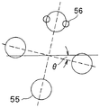
次に、本発明にかかる、試料修正方法の別の実施例について説明する。図3には、本発明にかかる、対物レンズによって細く絞った電子線をマスクに照射し、欠陥を修正する修正方法に用いられる電子線装置(電子線光学鏡筒)を簡略的に示している。カソード31は、Zr/O−WのショットキーカソードあるいはTaCの熱電界放出カソードを用いている。符号32は、ウェーネルトあるいはショットキーシールドを示し、符号33は、アノードを示している。電子銃は、カソード31と、ウェーネルトあるいはショットキーシールド32と、アノード33とから構成されており、Zr−Wショットキーカソード又はTaCカソード31から電子線を光軸外へ放出、例えば、光軸外の4つの方向へ放出する電子銃であり、この電子銃から放出された電子線は、コンデンサレンズ34で集束される。このコンデンサレンズ34は、電子線を集束させるだけでなく、後述するように方位角方向の回転量を調整可能な電磁レンズで作られている。
Next, another embodiment of the sample correcting method according to the present invention will be described. FIG. 3 schematically shows an electron beam apparatus (electron beam optical column) used in a correction method for correcting defects by irradiating a mask with an electron beam narrowed by an objective lens according to the present invention. . The
コンデンサレンズ34の試料(マスク)側には、成形開口板35が配設されている。この成形開口板35には、開口56が形成されている。この開口56は、図4に示すように、電子銃から光軸外の4つの方向へ各々放出された4つのビーム55のうち一つを通過させるように、光軸中心から外れた位置に成形開口板35に少なくとも一つ形成されている。従って、光軸上において電子銃側へ流れるイオンビームを遮断することができる。ビームは、成形開口板35のいずれか一つの開口56を通過し、縮小レンズ36と対物レンズ(対物レンズ用磁気レンズ)40とによって縮小されることにより、マスク(被修正試料)47上に直径が50nm程度の小径ビームとして照射される。すなわち、対物レンズ40によって細く絞った電子線がマスク47に照射される(電子銃から放出された電子線を少なくとも対物レンズにより細く絞り、試料に照射するステップ)。
A molded
静電偏向器37と、対物レンズ40の電子銃側の上部に設けられたE×B分離用及び走査用静電偏向器38の二段偏向器によって、マスク47上を2次元走査し、マスク47面(試料)から放出される2次電子を小開口43を通過させ、E×B分離用及び走査用静電偏向器38とE×B分離用偏向器(電磁偏向器)39で2次電子軌道52の方向へ偏向し、2次電子検出器(SE検出器)53で検出する。これによって、SEM像を取得することができ(試料のSEM像を取得するステップ)、該SEM像を監視して修正すべき場所を探すことができる。修正すべき場所を特定することができたら、その場所のみ走査を行い(試料のSEM像から該試料の修正すべき場所を探し、該修正すべき場所を電子線で走査するステップ)、ガス供給手段としてのガス導入管50から反応性ガスを導入して(試料上の電子線走査領域における反応性ガスの圧力を増加させるステップ)、エッチング(電子線アシストエッチング)又はデポジション(電子線アシストデポジション)を行う。また、修正が終了したら、再度SEM像を取得して修正が正確に行われているか否かの確認作業を行う(試料の修正が完了したことを確認するステップ)。
The
マスク47と対物レンズとの間には、圧力を制限する小開口(NA用及び圧力制限用開口)43が設けられているため、ガスが導入されるときでも小開口43によって電子銃側は高真空に保たれているのでビームがぼけることはなく、ビームを細く絞ることができ、微細な修正を行うことができる。また、小開口43とマスク47との間は距離が短いため、ビームはごく僅かしかボケない。
Since a small opening (NA and pressure limiting opening) 43 for limiting pressure is provided between the
上記電子線を細く絞る対物レンズ40は、磁気ギャップ42がマスク47側に形成されている磁気レンズ(電磁レンズ)40と、磁気レンズ40のマスク47側に設けられ、マスク47よりも高い電位を有する軸対称電極44とを備えている。マスク47には−4000V程度の負の電圧を与え、電極44には正の高電圧を与えるため、マスク47へのランディングエネルギーを1keV以下にしても、ビームを十分細く絞ることが可能である。また、走査時の軌道51は、小開口43の位置よりも電子銃側に偏向支点54を設けているので、偏向時の収差を小さくすることができる。
The
圧力壁45及び圧力隔壁46は、真空ポンプ(図示せず)と連結されている排管49と、ガス導入管50とを仕切る隔壁であり、絶縁材料で成形されている。また、圧力隔壁46の下方側には、圧力隔壁46との間隔が小さくなるようにガードリング48が設けられており、これによって、資料室側へもガスが多く流れないようになっている。また、Oリング41は、磁気レンズ40のコイルを真空から分離するために設けられている。
The
電子銃のZr/O−Wのショットキーカソードから光軸から角度を有する4つの方向へ放出されるビームの一つのみを用いるため高輝度で利用することができ、ビームを50nmに絞っても500nA以上のビーム電流を得ることができる。従って、高スループットで修理を行うことができると共に、終点検出のためにビームを絞っても良いS/N比でのSEM像を観察することができる。また、電子銃のZr−Wのショットキーカソードから光軸外の4つの方向へ放出されるビームの方位角θ方向のどの方向へ強いビーム55が出るのか不明であるため、図4に示すように、成形開口板35の開口56を、ビームの方位角θ方向に、かつ、成形開口板35上におけるビームの径幅の間隔をおいて複数(図示のものは、2つ)設けることができる。このようにすることにより、コンデンサレンズ(磁気レンズ)34での回転調整量を少なくすることができる。なお、本実施例では、SEM(走査型電子顕微鏡)型の検査装置を用いた例を示しているが、他の並列撮像の原理を用いた写像光学系の検査装置、イオンを用いたイオンビーム(電子線も含めて荷電粒子線という)光を用いた光線の検査装置にも適用可能である。
Since only one of the beams emitted from the Zr / O-W Schottky cathode of the electron gun in four directions having an angle from the optical axis is used, the beam can be used with high brightness. A beam current of 500 nA or more can be obtained. Therefore, repair can be performed with high throughput, and an SEM image can be observed at an S / N ratio where the beam may be narrowed for end point detection. Further, since it is unclear to which direction in the azimuth angle θ direction of the beam emitted from the Zr-W Schottky cathode of the electron gun in four directions off the optical axis, as shown in FIG. In addition, a plurality (two in the figure) of the
なお、上記各実施例では、マスクの修正について説明しているが、本発明は、これに限定されるものではなく、マスク以外の他の試料、例えば、最先端デバイスを製造中のウェーハ(デスクリートデバイスを製造中のGaAsウェーハ)についても適用可能である。 In each of the above embodiments, correction of a mask has been described. However, the present invention is not limited to this, and a sample other than the mask, for example, a wafer (desk) that is manufacturing a state-of-the-art device is described. The present invention can also be applied to a GaAs wafer for manufacturing a REIT device.
上述の試料修正方法で修正したマスクを用いることにより、デバイス製造方法において良好なリソグラフィを行うことができる。以下、図5及び図6を参照して、上述の試料修正方法で修正したマスクを用いることにより半導体デバイスを製造する方法の実施の形態について説明する。図5は、本発明による半導体デバイスの製造方法の一実施例を示すフローチャートである。この実施例の製造工程は以下の主工程を含んでいる。
(1)ウェーハを製造するウェーハ製造工程(又はウェーハを準備するウェーハ準備工程)(ステップ100)
(2)露光に使用するマスクを製造するマスク製造工程(又はマスクを準備するマスク準備工程)(ステップ101)
(3)ウェーハに必要な加工処理を行うウェーハプロセッシング工程(ステップ102)
(4)ウェーハ上に形成されたチップを1個ずつ切り出し、動作可能にならしめるチップ組立工程(ステップ103)
(5)組み立てられたチップを検査するチップ検査工程(ステップ104)
なお、上記のそれぞれの主工程は更に幾つかのサブ工程からなっている。
By using the mask corrected by the above-described sample correction method, good lithography can be performed in the device manufacturing method. Hereinafter, an embodiment of a method for manufacturing a semiconductor device by using a mask corrected by the above-described sample correction method will be described with reference to FIGS. FIG. 5 is a flowchart showing an embodiment of a semiconductor device manufacturing method according to the present invention. The manufacturing process of this embodiment includes the following main processes.
(1) Wafer manufacturing process for manufacturing a wafer (or wafer preparation process for preparing a wafer) (Step 100)
(2) Mask manufacturing process for manufacturing a mask used for exposure (or mask preparation process for preparing a mask) (Step 101)
(3) Wafer processing process for performing necessary processing on the wafer (Step 102)
(4) Chip assembly process for cutting out chips formed on the wafer one by one and making them operable (step 103)
(5) Chip inspection process for inspecting assembled chips (step 104)
Each of the main processes described above further includes several sub-processes.
これらの主工程中の中で、半導体デバイスの性能に決定的な影響を及ぼすのが(3)のウェーハプロセッシング工程である。この工程では、設計された回路パターンをウェーハ上に順次積層し、メモリやMPUとして動作するチップを多数形成する。このウェーハプロセッシング工程は以下の各工程を含んでいる。
(A)絶縁層となる誘電体薄膜や配線部、或いは電極部を形成する金属薄膜等を形成する薄膜形成工程(CVDやスパッタリング等を用いる)
(B)この薄膜層を形成する別の手段であるウェーハ基板を酸化する酸化工程
(C)薄膜層やウェーハ基板等を選択的に加工するためにマスク(レチクル)を用いてレジストパターンを形成するリソグラフィー工程
(D)レジストパターンに従って薄膜層や基板を加工するエッチング工程(例えばドライエッチング技術を用いる)
(E)イオン・不純物注入拡散工程
(F)レジスト剥離工程
(G)加工されたウェーハを検査する工程
なお、ウェーハプロセッシング工程は必要な層数だけ繰り返し行い、設計通り動作する半導体デバイスを製造する。
Among these main processes, the wafer processing process (3) has a decisive influence on the performance of the semiconductor device. In this process, designed circuit patterns are sequentially stacked on a wafer to form a large number of chips that operate as memories and MPUs. This wafer processing process includes the following processes.
(A) A thin film forming process for forming a dielectric thin film to be an insulating layer, a wiring portion, or a metal thin film for forming an electrode portion (using CVD, sputtering, etc.)
(B) An oxidation process for oxidizing the wafer substrate, which is another means for forming the thin film layer. (C) A resist pattern is formed using a mask (reticle) to selectively process the thin film layer, the wafer substrate, or the like. Lithography process (D) Etching process (for example, using dry etching technology) that processes a thin film layer or a substrate according to a resist pattern
(E) Ion / impurity implantation / diffusion process (F) Resist stripping process (G) Process for inspecting a processed wafer The wafer processing process is repeated as many times as necessary to manufacture a semiconductor device that operates as designed.
図6は、上記ウェーハプロセッシング工程の中核をなすリソグラフィー工程を示すフローチャートである。このリソグラフィー工程は以下の各工程を含む。
(a)前段の工程で回路パターンが形成されたウェーハ上にレジストをコートするレジスト塗布工程(ステップ200)
(b)レジストを露光する工程(ステップ201)
(c)露光されたレジストを現像してレジストのパターンを得る現像工程(ステップ202)
(d)現像されたレジストパターンを安定化するためのアニール工程(ステップ203)
上記の半導体デバイス製造工程、ウェーハプロセッシング工程、リソグラフィー工程については、周知のものでありこれ以上の説明を要しないであろう。
FIG. 6 is a flowchart showing a lithography process which forms the core of the wafer processing process. This lithography process includes the following steps.
(A) A resist coating process for coating a resist on the wafer on which the circuit pattern is formed in the preceding process (step 200).
(B) Step of exposing resist (step 201)
(C) Development step of developing the exposed resist to obtain a resist pattern (step 202)
(D) An annealing step for stabilizing the developed resist pattern (step 203)
The above semiconductor device manufacturing process, wafer processing process, and lithography process are well known and need no further explanation.
上記(G)の検査工程に本発明に係る欠陥検査方法、欠陥検査装置を用いると、微細なパターンを有する半導体デバイスでも、スループット良く検査できるので、全数検査が可能となり、製品の歩留まりの向上、欠陥製品の出荷防止が可能と成る。 When the defect inspection method and the defect inspection apparatus according to the present invention are used in the inspection step (G), even a semiconductor device having a fine pattern can be inspected with high throughput, so that 100% inspection is possible, and the yield of products is improved. It becomes possible to prevent shipment of defective products.
1 Zr−Wチップ 2 ショットキーシールド
3 チップ加熱用Wフィラメント 4 コンデンサレンズ
5 成形開口板 6 矩形開口
7 矩形開口 8 NA開口
9 縮小レンズ 10 対物レンズ
11 高真空排気管 12 低真空排気管
13 ガス注入管 14 低真空排気管
15 負電源 16 マスク
17 冷却ガス 18 E×B分離器
19 2次電子検出器(SE検出器) 20 偏向器
21 Crパターン 22 黒欠陥
23 成形ビーム 23’ 成形ビーム
26 白欠陥 31 カソード
32 ウェーネルトあるいはショットキーシールド
33 アノード 34 コンデンサレンズ
35 成形開口板 36 縮小レンズ
37 静電偏向器 38 E×B分離用及び走査用静電偏向器
39 E×B分離用偏向器(電磁偏向器)
40 対物レンズ 41 Oリング
42 磁気ギャップ 43 小開口
44 軸対称電極 45 圧力壁
46 圧力隔壁 47 マスク
48 ガードリング 49 排管
50 ガス導入管 51 軌道
52 2次電子軌道 53 2次電子検出器(SE検出器)
54 偏向支点 56 開口
DESCRIPTION OF
40 Objective Lens 41 O-
54
Claims (17)
(a)電子線を対物レンズにより集束して試料に照射するステップと、
(b)前記試料の電子線照射面に反応性ガスを供給するステップと、
(c)前記試料の被修正パターンに電子線を選択的に走査してエッチング又は堆積により修正を行うステップと、
(d)前記電子線照射面に供給された反応性ガスが電子銃側へ流入するのを制限するように、前記対物レンズに設けた差動排気装置で排気し続けるステップとを備えていることを特徴とする試料修正方法。 A sample correction method comprising:
(A) focusing the electron beam with an objective lens and irradiating the sample;
(B) supplying a reactive gas to the electron beam irradiation surface of the sample;
(C) selectively correcting the pattern to be corrected of the sample by scanning an electron beam and etching or depositing;
(D) including a step of continuously exhausting the reactive gas supplied to the electron beam irradiation surface by a differential exhaust device provided in the objective lens so as to restrict the reactive gas supplied to the electron gun side. A sample correction method characterized by the above.
(a)電子銃から放出された電子線を対物レンズに通過させ、試料に照射するステップと、
(b)前記試料表面の画像を取得するステップと、
(c)前記試料表面の画像から該試料の修正すべき場所を探し、該修正すべき場所を電子線で走査するステップと、
(d)前記試料上の電子線走査領域における反応性ガスの圧力を増加させるステップと、
(e)前記試料の修正が完了したことを確認するステップとを備え、
前記試料と前記対物レンズとの間に、圧力を制限する小開口が設けられていることを特徴とする試料修正方法。 A sample correction method comprising:
(A) passing the electron beam emitted from the electron gun through the objective lens and irradiating the sample;
(B) obtaining an image of the sample surface;
(C) searching for a location to be corrected of the sample from the image of the sample surface, and scanning the location to be corrected with an electron beam;
(D) increasing the pressure of the reactive gas in the electron beam scanning region on the sample;
(E) confirming that the correction of the sample is completed,
A sample correction method, wherein a small opening for limiting pressure is provided between the sample and the objective lens.
磁気ギャップが試料側に形成されている磁気レンズと、
前記磁気レンズの試料側に設けられ、該試料よりも高い電位を有する軸対称電極とを備えていることを特徴とする、請求項5に記載の試料修正方法。 The objective lens for narrowing the electron beam is:
A magnetic lens having a magnetic gap formed on the sample side;
The sample correction method according to claim 5, further comprising an axially symmetric electrode provided on the sample side of the magnetic lens and having a higher potential than the sample.
前記試料表面の画像を取得する取得ステップは、前記試料から放出された2次電子を前記E×B分離器で偏向して検出器で検出することにより、該試料表面の画像を取得することを特徴とする、請求項5に記載の試料修正方法。 On the electron gun side or inside of the objective lens, an E × B separator is provided,
The acquisition step of acquiring an image of the sample surface is to acquire an image of the sample surface by deflecting secondary electrons emitted from the sample with the E × B separator and detecting with the detector. The sample correction method according to claim 5, wherein the sample correction method is characterized.
電子線を集束して試料に照射する対物レンズと、
前記試料の電子線照射面に反応性ガスを供給するガス供給手段と、
前記対物レンズに設けられ、前記供給手段によって前記電子線照射面に供給された反応性ガスが電子銃側へ流入するのを制限するように該反応性ガスを排気し続ける差動排気装置とを備え、
前記試料の被修正パターンに電子線を選択的に走査してエッチング又は堆積により修正を行うことを特徴とする試料修正装置。 A sample correction device for correcting a sample,
An objective lens that focuses the electron beam and irradiates the sample;
Gas supply means for supplying a reactive gas to the electron beam irradiation surface of the sample;
A differential evacuation device that is provided on the objective lens and continues to exhaust the reactive gas so as to restrict the reactive gas supplied to the electron beam irradiation surface by the supply means from flowing into the electron gun side; Prepared,
An apparatus for correcting a sample, wherein the pattern to be corrected is selectively scanned by an electron beam and corrected by etching or deposition.
前記成形開口手段は、
前記コンデンサレンズによって集束された電子線をx方向及びy方向に平行な辺を有する矩形に成形する第1成形開口と、
前記コンデンサレンズによって集束された電子線をx方向及びy方向に対して所定の角度に傾斜した辺を有する矩形に成形する第2成形開口とを備え、
前記第1成形開口と前記第2成形開口は切り替え可能となっていることを特徴とする、請求項10に記載の試料修正装置。 A condenser lens is further provided after the electron gun, and a molding opening means is provided before or after the condenser lens.
The shaping opening means is
A first shaping opening for shaping the electron beam focused by the condenser lens into a rectangle having sides parallel to the x direction and the y direction;
A second shaping opening for shaping the electron beam focused by the condenser lens into a rectangle having sides inclined at a predetermined angle with respect to the x direction and the y direction;
The sample correction apparatus according to claim 10, wherein the first molding opening and the second molding opening are switchable.
電子線を放出する電子銃と、
前記電子銃から放出された前記電子線を集束して前記試料に照射する対物レンズと、
前記試料表面の画像を取得する画像取得手段と、
前記試料の電子線照射面に反応性ガスを供給し、該試料上の電子線走査領域における反応性ガスの圧力を増加させるガス供給手段と、
前記試料と前記対物レンズとの間に設けられた、前記反応性ガスの圧力を制限する小開口とを備え、
前記画像取得手段によって取得された前記試料表面の画像から該試料の修正すべき場所を探し、且つ修正すべきパターンの方向を測定し、該修正すべき場所を電子線で上記パターン辺に平行に走査してエッチング又は堆積により修正を行うことを特徴とする試料修正装置。 A sample correction device for correcting a sample,
An electron gun that emits an electron beam;
An objective lens that focuses the electron beam emitted from the electron gun and irradiates the sample;
Image acquisition means for acquiring an image of the sample surface;
A gas supply means for supplying a reactive gas to the electron beam irradiation surface of the sample and increasing the pressure of the reactive gas in the electron beam scanning region on the sample;
A small opening provided between the sample and the objective lens for limiting the pressure of the reactive gas;
The location of the sample to be corrected is searched from the image of the sample surface acquired by the image acquisition means, the direction of the pattern to be corrected is measured, and the location to be corrected is parallel to the pattern side with an electron beam. A sample correcting device which performs correction by scanning or etching.
磁気ギャップが試料側に形成されている磁気レンズと、
前記磁気レンズの試料側に設けられ、該試料よりも高い電位を有する軸対称電極とを備えていることを特徴とする、請求項14に記載の試料修正装置。 The objective lens for narrowing the electron beam is:
A magnetic lens having a magnetic gap formed on the sample side;
The sample correcting device according to claim 14, further comprising an axially symmetric electrode provided on a sample side of the magnetic lens and having a higher potential than the sample.
前記試料表面の画像を取得する前記画像取得手段は、前記試料から放出された2次電子を前記E×B分離器で偏向して検出器で検出することにより、該試料表面の画像を取得することを特徴とする、請求項14に記載の試料修正方法。 On the electron gun side or inside of the objective lens, an E × B separator is provided,
The image acquisition means for acquiring an image of the sample surface acquires an image of the sample surface by deflecting secondary electrons emitted from the sample with the E × B separator and detecting them with a detector. The sample correction method according to claim 14, wherein:
Priority Applications (2)
| Application Number | Priority Date | Filing Date | Title |
|---|---|---|---|
| JP2004011787A JP2005208120A (en) | 2004-01-20 | 2004-01-20 | Sample correcting apparatus, sample correction method, and device manufacturing method using the method |
| US11/037,093 US7256405B2 (en) | 2004-01-20 | 2005-01-19 | Sample repairing apparatus, a sample repairing method and a device manufacturing method using the same method |
Applications Claiming Priority (1)
| Application Number | Priority Date | Filing Date | Title |
|---|---|---|---|
| JP2004011787A JP2005208120A (en) | 2004-01-20 | 2004-01-20 | Sample correcting apparatus, sample correction method, and device manufacturing method using the method |
Publications (2)
| Publication Number | Publication Date |
|---|---|
| JP2005208120A true JP2005208120A (en) | 2005-08-04 |
| JP2005208120A5 JP2005208120A5 (en) | 2007-02-01 |
Family
ID=34898377
Family Applications (1)
| Application Number | Title | Priority Date | Filing Date |
|---|---|---|---|
| JP2004011787A Ceased JP2005208120A (en) | 2004-01-20 | 2004-01-20 | Sample correcting apparatus, sample correction method, and device manufacturing method using the method |
Country Status (2)
| Country | Link |
|---|---|
| US (1) | US7256405B2 (en) |
| JP (1) | JP2005208120A (en) |
Cited By (2)
| Publication number | Priority date | Publication date | Assignee | Title |
|---|---|---|---|---|
| JP2007234583A (en) * | 2006-01-31 | 2007-09-13 | Toshiba Corp | Charged particle beam apparatus and defect correcting method |
| US7692163B2 (en) | 2006-01-31 | 2010-04-06 | Kabushiki Kaisha Toshiba | Charged particle beam apparatus, defect correcting method, etching method, deposition method, and charge preventing method |
Families Citing this family (14)
| Publication number | Priority date | Publication date | Assignee | Title |
|---|---|---|---|---|
| DE10353591A1 (en) * | 2003-11-17 | 2005-06-02 | Infineon Technologies Ag | Method for locally limited etching of a chromium layer |
| US7670956B2 (en) * | 2005-04-08 | 2010-03-02 | Fei Company | Beam-induced etching |
| WO2007051313A1 (en) * | 2005-11-07 | 2007-05-10 | Fibics Incorporated | Methods for performing circuit edit operations with low landing energy electron beams |
| US7892978B2 (en) * | 2006-07-10 | 2011-02-22 | Micron Technology, Inc. | Electron induced chemical etching for device level diagnosis |
| US7791055B2 (en) | 2006-07-10 | 2010-09-07 | Micron Technology, Inc. | Electron induced chemical etching/deposition for enhanced detection of surface defects |
| US7807062B2 (en) * | 2006-07-10 | 2010-10-05 | Micron Technology, Inc. | Electron induced chemical etching and deposition for local circuit repair |
| US7718080B2 (en) * | 2006-08-14 | 2010-05-18 | Micron Technology, Inc. | Electronic beam processing device and method using carbon nanotube emitter |
| US7833427B2 (en) * | 2006-08-14 | 2010-11-16 | Micron Technology, Inc. | Electron beam etching device and method |
| US7791071B2 (en) | 2006-08-14 | 2010-09-07 | Micron Technology, Inc. | Profiling solid state samples |
| DE102007054074A1 (en) * | 2007-11-13 | 2009-05-14 | Carl Zeiss Nts Gmbh | System for editing an object |
| JP5709535B2 (en) * | 2011-01-07 | 2015-04-30 | キヤノン株式会社 | Electron beam drawing apparatus and article manufacturing method using the same |
| KR102069183B1 (en) * | 2012-03-20 | 2020-01-22 | 에이에스엠엘 네델란즈 비.브이. | Arrangement and method for transporting radicals |
| CN106680305B (en) * | 2016-11-23 | 2023-08-04 | 聚束科技(北京)有限公司 | Vacuum atmosphere treatment device, sample observation system and method |
| UA122437C2 (en) * | 2018-11-06 | 2020-11-10 | Приватне Акціонерне Товариство "Нво "Червона Хвиля" | DEVICE FOR MANUFACTURE OF THREE-DIMENSIONAL OBJECTS |
Family Cites Families (4)
| Publication number | Priority date | Publication date | Assignee | Title |
|---|---|---|---|---|
| US5429730A (en) * | 1992-11-02 | 1995-07-04 | Kabushiki Kaisha Toshiba | Method of repairing defect of structure |
| US6392333B1 (en) * | 1999-03-05 | 2002-05-21 | Applied Materials, Inc. | Electron gun having magnetic collimator |
| US7138629B2 (en) * | 2003-04-22 | 2006-11-21 | Ebara Corporation | Testing apparatus using charged particles and device manufacturing method using the testing apparatus |
| US7420164B2 (en) * | 2004-05-26 | 2008-09-02 | Ebara Corporation | Objective lens, electron beam system and method of inspecting defect |
-
2004
- 2004-01-20 JP JP2004011787A patent/JP2005208120A/en not_active Ceased
-
2005
- 2005-01-19 US US11/037,093 patent/US7256405B2/en not_active Expired - Fee Related
Cited By (3)
| Publication number | Priority date | Publication date | Assignee | Title |
|---|---|---|---|---|
| JP2007234583A (en) * | 2006-01-31 | 2007-09-13 | Toshiba Corp | Charged particle beam apparatus and defect correcting method |
| US7692163B2 (en) | 2006-01-31 | 2010-04-06 | Kabushiki Kaisha Toshiba | Charged particle beam apparatus, defect correcting method, etching method, deposition method, and charge preventing method |
| JP4543047B2 (en) * | 2006-01-31 | 2010-09-15 | 株式会社東芝 | Charged beam apparatus and defect correction method |
Also Published As
| Publication number | Publication date |
|---|---|
| US7256405B2 (en) | 2007-08-14 |
| US20050211925A1 (en) | 2005-09-29 |
Similar Documents
| Publication | Publication Date | Title |
|---|---|---|
| US7256405B2 (en) | Sample repairing apparatus, a sample repairing method and a device manufacturing method using the same method | |
| JP5925404B2 (en) | Electron microscope for inspecting and processing an object having a miniaturized structure, and method for manufacturing the object | |
| US7005641B2 (en) | Electron beam apparatus and a device manufacturing method by using said electron beam apparatus | |
| US7312449B2 (en) | Electron beam system and method of manufacturing devices using the system | |
| US7189979B2 (en) | Electron gun | |
| JP5779210B2 (en) | Charged particle beam inspection method and apparatus | |
| US10249472B2 (en) | Charged particle beam device, charged particle beam influencing device, and method of operating a charged particle beam device | |
| JP2002141010A (en) | Electron beam device and manufacturing method of device using the same | |
| JP2003187733A (en) | Electron beam apparatus and method for manufacturing device using the same | |
| JP3995479B2 (en) | Electron beam apparatus and device manufacturing method using the electron beam apparatus | |
| JP2006054192A (en) | Electron beam device and device manufacturing method using the same | |
| JP4012429B2 (en) | Electron beam apparatus and device manufacturing method using the same | |
| JP4230280B2 (en) | Defect inspection method and device manufacturing method using the inspection method | |
| JP2006019326A (en) | Pattern formation method, mask repair method and method for manufacturing device using them | |
| JP2003297272A (en) | Electron beam apparatus and method of manufacturing device using the same | |
| JP2003142020A (en) | Electron beam device and manufacturing method for device using the electron beam device | |
| JP2003132832A (en) | Electron beam system, method for inspecting defect, and method for manufacturing device using the system and the method | |
| JP2007251024A (en) | Charged beam exposure apparatus, charged beam exposure method, and method of manufacturing semiconductor device | |
| JP2003323860A (en) | Electron beam equipment and manufacturing method of device using the same | |
| JP2003168385A (en) | Electron beam device and device manufacturing method using it | |
| JP2003208867A (en) | Electron beam device, defect inspection method and device, and device manufacturing method therewith | |
| JP2005276881A (en) | Pattern evaluation method and device manufacturing method using it | |
| JP2000348662A (en) | Charged particle beam irradiating system, charged particle beam exposure device and manufacture of semiconductor device | |
| JP2004200111A (en) | Electron beam device and manufacturing method of device using the device | |
| JP2003123679A (en) | Electron beam equipment and device-manufacturing method using same electron beam equipment |
Legal Events
| Date | Code | Title | Description |
|---|---|---|---|
| A521 | Request for written amendment filed |
Free format text: JAPANESE INTERMEDIATE CODE: A523 Effective date: 20061208 |
|
| A621 | Written request for application examination |
Free format text: JAPANESE INTERMEDIATE CODE: A621 Effective date: 20061208 |
|
| A01 | Written decision to grant a patent or to grant a registration (utility model) |
Free format text: JAPANESE INTERMEDIATE CODE: A01 Effective date: 20090803 |
|
| A045 | Written measure of dismissal of application [lapsed due to lack of payment] |
Free format text: JAPANESE INTERMEDIATE CODE: A045 Effective date: 20091216 |