JP2005200737A - Method of forming transparent electroconductive film - Google Patents
Method of forming transparent electroconductive film Download PDFInfo
- Publication number
- JP2005200737A JP2005200737A JP2004010271A JP2004010271A JP2005200737A JP 2005200737 A JP2005200737 A JP 2005200737A JP 2004010271 A JP2004010271 A JP 2004010271A JP 2004010271 A JP2004010271 A JP 2004010271A JP 2005200737 A JP2005200737 A JP 2005200737A
- Authority
- JP
- Japan
- Prior art keywords
- transparent conductive
- conductive film
- gas
- electric field
- forming
- Prior art date
- Legal status (The legal status is an assumption and is not a legal conclusion. Google has not performed a legal analysis and makes no representation as to the accuracy of the status listed.)
- Pending
Links
Images


Classifications
-
- Y—GENERAL TAGGING OF NEW TECHNOLOGICAL DEVELOPMENTS; GENERAL TAGGING OF CROSS-SECTIONAL TECHNOLOGIES SPANNING OVER SEVERAL SECTIONS OF THE IPC; TECHNICAL SUBJECTS COVERED BY FORMER USPC CROSS-REFERENCE ART COLLECTIONS [XRACs] AND DIGESTS
- Y02—TECHNOLOGIES OR APPLICATIONS FOR MITIGATION OR ADAPTATION AGAINST CLIMATE CHANGE
- Y02E—REDUCTION OF GREENHOUSE GAS [GHG] EMISSIONS, RELATED TO ENERGY GENERATION, TRANSMISSION OR DISTRIBUTION
- Y02E10/00—Energy generation through renewable energy sources
- Y02E10/50—Photovoltaic [PV] energy
Abstract
Description
本発明は、液晶表示素子、有機エレクトロルミネッセンス素子(以下、有機EL素子という。)、プラズマディスプレイパネル(以下、PDPという。)、電子ペーパー、タッチパネル、太陽電池等の各種エレクトロニクス素子に好適に用いられる透明導電膜の形成方法に関する。 The present invention is suitably used for various electronic elements such as liquid crystal display elements, organic electroluminescence elements (hereinafter referred to as organic EL elements), plasma display panels (hereinafter referred to as PDPs), electronic paper, touch panels, solar cells and the like. The present invention relates to a method for forming a transparent conductive film.
従来より、液晶表示素子、有機EL素子、太陽電池、タッチパネル、電磁波シールド材、赤外線反射膜等に透明導電膜は広く使用されている。 Conventionally, transparent conductive films have been widely used for liquid crystal display elements, organic EL elements, solar cells, touch panels, electromagnetic wave shielding materials, infrared reflective films, and the like.
透明導電膜としては、Pt、Au、Ag、Cu等の金属薄膜、SnO2、In2O3、CdO、ZnO2、SnO2:Sb、SnO2:F、ZnO:Al、In2O3:Snなどの酸化物及びドーパントによる複合酸化物膜、カルコゲナイド、LaB6、TiN、TiC等の非酸化物膜が用いられている。中でも、錫をドープした酸化インジウム膜(ITO膜)が、優れた電気特性を有し、エッチングによる加工が容易であることなどからしてもっとも広く使用されている。 As the transparent conductive film, a metal thin film such as Pt, Au, Ag, or Cu, SnO 2 , In 2 O 3 , CdO, ZnO 2 , SnO 2 : Sb, SnO 2 : F, ZnO: Al, In 2 O 3 : A composite oxide film made of an oxide such as Sn and a dopant, or a non-oxide film such as chalcogenide, LaB 6 , TiN, or TiC is used. Among them, an indium oxide film doped with tin (ITO film) is most widely used because it has excellent electrical characteristics and is easily processed by etching.
これらの透明導電膜は、真空蒸着法やスパッタリング法,イオンプレーティング法、真空プラズマCVD法、スプレーパイロリシス法、熱CVD法、ゾルゲル法等により形成することができる。 These transparent conductive films can be formed by vacuum deposition, sputtering, ion plating, vacuum plasma CVD, spray pyrolysis, thermal CVD, sol-gel, or the like.
近年、液晶表示素子、有機EL素子等のフラットパネルディスプレイにおいては大面積化、高精細化が進んでおりより高性能な透明導電膜が求められるようになってきている。特に、液晶表示素子においては、高い電界応答性を有する素子や装置が求められており、そのために、電子移動度の高い透明導電膜が求められている。また、有機EL素子においては、電流駆動方式がとられるために、より低抵抗な透明導電膜が求められている。 2. Description of the Related Art In recent years, flat panel displays such as liquid crystal display elements and organic EL elements have been increased in area and definition, and a higher performance transparent conductive film has been demanded. In particular, in liquid crystal display elements, elements and devices having high electric field responsiveness are required, and for that purpose, transparent conductive films having high electron mobility are required. Moreover, in an organic EL element, since a current drive system is adopted, a transparent conductive film having a lower resistance is required.
上記の透明導電膜の形成方法の中でも、真空蒸着法やスパッタリング法は、低抵抗な透明導電膜を得ることができ、工業的には、DCマグネトロンスパッタリング装置を用いて比抵抗値が10-4Ω・cmオーダーの優れた導電性を有するITO膜を得ることができる。 Among the methods for forming the transparent conductive film, the vacuum deposition method and the sputtering method can obtain a low-resistance transparent conductive film, and industrially, the specific resistance value is 10 −4 using a DC magnetron sputtering apparatus. An ITO film having excellent conductivity on the order of Ω · cm can be obtained.
しかしながら、これらの物理的製作法(PVD法)は、気相中で目的物質を基板に堆積させて膜を成長させるものであり、真空装置を使用しなければならず、そのために装置が大がかりで高価となり、また、原料の使用効率が悪くて生産性も低く、大面積の膜を得ることも困難であった。さらに、低抵抗品を得るためには、製膜時に200〜300℃に加熱する必要があり、プラスチックフィルム上に、低抵抗な透明導電膜の形成することは困難である。 However, these physical fabrication methods (PVD method) are intended to grow a film by depositing a target substance on a substrate in a gas phase, and a vacuum apparatus must be used. It was expensive, and the raw material use efficiency was poor, the productivity was low, and it was difficult to obtain a large-area film. Furthermore, in order to obtain a low-resistance product, it is necessary to heat to 200 to 300 ° C. during film formation, and it is difficult to form a low-resistance transparent conductive film on a plastic film.
また、ゾルゲル法(塗布法)は、分散調液、塗布、乾燥といった多くのプロセスが必要であるだけでなく、被処理基材との接着性が低いために、バインダー樹脂を使用することが必要で、透明性が悪くなってしまう。また、得られた透明導電膜膜の電気特性もPVD法を用いた場合に比較すると劣っている。 The sol-gel method (coating method) not only requires many processes such as dispersion preparation, coating, and drying, but also requires the use of a binder resin because of its low adhesion to the substrate to be treated. Therefore, the transparency is deteriorated. Moreover, the electrical characteristics of the obtained transparent conductive film are also inferior compared with the case where the PVD method is used.
また、熱CVD法は、気化した原材料あるいは原材料溶液を基板に吹きつけ、熱分解させることで膜を形成するものであり、装置が簡単で生産性に優れ、大面積の成膜が容易に行えるという利点があるが、通常、焼成時に400℃から500℃での高温処理を必要とするため使用する基材が限られてしまうという問題点を有していた。特に、プラスチックフィルム基板への成膜は困難であった。 The thermal CVD method forms a film by spraying vaporized raw materials or raw material solutions onto a substrate and thermally decomposing them. The apparatus is simple, the productivity is high, and a large area can be easily formed. However, there is a problem that the base material to be used is limited because high temperature treatment at 400 to 500 ° C. is usually required at the time of firing. In particular, film formation on a plastic film substrate was difficult.
上記のゾルゲル法(塗布法)では高機能な薄膜が得られにくい、また、真空装置を用いる方法では生産性が悪いというデメリットを克服する方法として、大気圧または大気圧近傍の圧力下で放電し、反応性ガスをプラズマ励起し、基材上に薄膜を形成する方法(以下、大気圧プラズマCVD法という。)が提案され、特開2000−303175号公報には大気圧プラズマCVD法により透明導電膜を形成する技術が開示されている。 The above sol-gel method (coating method) is difficult to obtain a high-performance thin film, and as a method of overcoming the disadvantage that productivity is poor in a method using a vacuum apparatus, discharge is performed at atmospheric pressure or near atmospheric pressure. A method of forming a thin film on a substrate (hereinafter referred to as an atmospheric pressure plasma CVD method) by exciting a reactive gas with plasma is proposed. A technique for forming a film is disclosed.
大気圧プラズマCVD法について、これまで種々の検討が行われ、希ガスと透明導電膜を形成する金属化合物ガスを含有する混合ガスを使用して、高品位の透明導電膜を得ることができることがわかってきた(例えば、特開2002−155371(特許文献1))。しかしながら、大気圧プラズマCVD法においては、放電ガスに使用しているヘリウムやアルゴンが高価なためこれがコストアップの大きな原因になっている。 Various studies have been conducted on atmospheric pressure plasma CVD, and a high-quality transparent conductive film can be obtained by using a mixed gas containing a rare gas and a metal compound gas that forms a transparent conductive film. It has been understood (for example, JP-A-2002-155371 (Patent Document 1)). However, in the atmospheric pressure plasma CVD method, helium and argon used for the discharge gas are expensive, which causes a significant increase in cost.
大気圧プラズマCVD法においては、放電ガスとして希ガス以外の安価なガス、例えば、空気成分中の酸素ガス、窒素ガスや二酸化炭素等を使用する場合、放電を開始する電界の強さ(以下、電界強度とも言う)が高く、従来の高周波電界のもとでは安定な放電が得られず、薄膜が形成されにくかったが、例えば、特開平10−154598号公報には、パルス電界を用いることにより、窒素ガスのような放電開始電界強度の高いガスでも放電が達成出来ることが開示されており、また、特開平11−191576号公報には、窒素ガスを用い、高周波電界と低周波電界とを重畳させ発生したプラズマによって基材を洗浄する工程を有する電子部品実装方法が開示されている。更に、特開2001−74906(特許文献2)においては、低周波の100kHzのパルスを用いた、N2ガスによる大気圧プラズマ法が記載されている。 In the atmospheric pressure plasma CVD method, when an inexpensive gas other than a rare gas is used as a discharge gas, for example, oxygen gas, nitrogen gas or carbon dioxide in an air component, the strength of an electric field for starting discharge (hereinafter, Although the electric field strength is high), a stable discharge cannot be obtained under a conventional high-frequency electric field, and it is difficult to form a thin film. For example, Japanese Patent Application Laid-Open No. 10-154598 uses a pulse electric field. Further, it is disclosed that a discharge can be achieved even with a gas having a high discharge starting electric field strength such as nitrogen gas, and Japanese Patent Application Laid-Open No. 11-191576 uses a nitrogen gas to provide a high frequency electric field and a low frequency electric field. An electronic component mounting method including a step of cleaning a base material with plasma generated by superposition is disclosed. Furthermore, JP-A-2001-74906 (Patent Document 2) describes an atmospheric pressure plasma method using N 2 gas using a low-frequency 100 kHz pulse.
これら窒素ガスを放電ガスとして用いた大気圧プラズマ法を用いることにより、安価に透明導電膜を形成できるが、これら窒素を放電ガスとして用いて形成した透明導電膜においては、高性能なものを得ることが難しいことがわかってきた。 A transparent conductive film can be formed at low cost by using the atmospheric pressure plasma method using these nitrogen gases as a discharge gas. However, a transparent conductive film formed using these nitrogen gases as a discharge gas has a high performance. I found it difficult.
この要因は、窒素ガスなどの活性ガスを用いると膜中にコンタミ(不純物)として炭素(C),窒素(N)が含有されやすく、これらがキャリア密度、移動度を低下させ、抵抗率を増加させるためであると考えられる。窒素ガスを放電ガスとして用いた方法においては、未だにスパッタ並みの性能をもった透明導電膜は得られていない。 The reason for this is that when an active gas such as nitrogen gas is used, carbon (C) and nitrogen (N) are likely to be contained in the film as impurities (impurities), which lower the carrier density and mobility, and increase the resistivity. It is thought that it is to make it. In the method using nitrogen gas as the discharge gas, a transparent conductive film having performance equivalent to that of sputtering has not yet been obtained.
本発明者らは、反応性ガスの主成分が酸素原子を含む特定の無機ガスを加えることにより、膜中に含有されるN,Cを低減させ、窒素ガスを用いた大気圧プラズマにおいて高性能な透明導電膜を作成することに成功した。これはスパッタ堆積された透明導電膜の性能と同程度であり、更に安価な窒素ガスを使用しているため、低コストで作製可能であり、生産性の高い方法である。
従って、本発明の目的は、安全性が高く、生産性に優れ、良好な光学特性及び電気特性を有し、プラスチックフィルム基材上での優れた機械的耐性を有する透明導電膜形成方法並びに透明導電膜及び透明導電膜を有する物品を提供することにある。 Accordingly, an object of the present invention is to provide a method for forming a transparent conductive film, which has high safety, excellent productivity, good optical properties and electrical properties, and excellent mechanical resistance on a plastic film substrate. The object is to provide an article having a conductive film and a transparent conductive film.
(請求項1)
大気圧または大気圧近傍の圧力下において、反応性ガス及び放電ガスを電極間の放電空間に導入し、電極間に高周波電界を印加して、プラズマ状態とし、前記放電空間において、基材を前記プラズマ状態の反応性ガスに晒し、基材上に透明導電膜を形成する透明導電膜形成方法において、反応性ガスが分子内に少なくとも1つの酸素原子を有する無機ガスと有機金属化合物を含有する混合ガスであり、放電ガスが窒素であることを特徴とする透明導電膜形成方法。
(Claim 1)
Under an atmospheric pressure or a pressure near atmospheric pressure, a reactive gas and a discharge gas are introduced into the discharge space between the electrodes, a high frequency electric field is applied between the electrodes to form a plasma state, and the substrate is In a method of forming a transparent conductive film by exposing to a reactive gas in a plasma state and forming a transparent conductive film on a substrate, the reactive gas contains an inorganic gas having at least one oxygen atom in the molecule and an organometallic compound A method for forming a transparent conductive film, which is a gas and the discharge gas is nitrogen.
(請求項2)
高周波電界が印加される電極の間に形成される空間および印加された高周波電界により形成されるプラズマ状態の反応性ガスが基材と接触する空間を含む放電空間の周囲の雰囲気中の酸素濃度が5体積%以下であることを特徴とする請求項1に記載の透明導電膜形成方法。
(Claim 2)
The oxygen concentration in the atmosphere around the discharge space including the space formed between the electrodes to which the high-frequency electric field is applied and the space in which the reactive gas in the plasma state formed by the applied high-frequency electric field is in contact with the substrate It is 5 volume% or less, The transparent conductive film formation method of Claim 1 characterized by the above-mentioned.
(請求項3)
前記有機金属化合物が以下の一般式1または一般式2で表される有機金属化合物であることを特徴とする請求項1または2に記載の透明導電膜形成方法。
(Claim 3)
The method for forming a transparent conductive film according to claim 1, wherein the organometallic compound is an organometallic compound represented by the following general formula 1 or

〔一般式1及び2において、MはIn、Sn、Znを表し、R1、R2はそれぞれ置換基を有していてもよいアルキル基、アリール基、アルコキシル基を表し、Rは水素原子、置換基を表し、また、RはR1、R2と結合して環を形成してもよい。R3はそれぞれ置換基を有していてもよいアルキル基、アリール基を表す。n1は整数を表し、n2は整数を表す。〕
(請求項4)
前記高周波電界が、第1の高周波電界および第2の高周波電界を重畳したものであり、
前記第1の高周波電界の周波数ω1より前記第2の高周波電界の周波数ω2が高く、前記第1の高周波電界の強さV1、前記第2の高周波電界の強さV2および放電開始電界の強さIVとの関係が、
V1≧IV>V2
または、V1>IV≧V2 を満たすことを特徴とする請求項1〜3のいずれか1項に記載の透明導電膜形成方法。
(請求項5)
前記放電空間が、対向する第1電極と第2電極とで構成されることを特徴とする請求項4に記載の透明導電膜形成方法。
(請求項6)
前記第2の高周波電界の出力密度が、50W/cm2以下であることを特徴とする請求項4または5に記載の透明導電膜形成方法。
(請求項7)
前記第2の高周波電界の出力密度が、20W/cm2以下であることを特徴とする請求項6に記載の透明導電膜形成方法。
(請求項8)
前記第1の高周波電界の出力密度が1W/cm2以上であることを特徴とする請求項4〜7のいずれか1項に記載の透明導電膜形成方法。
(請求項9)
前記第1の高周波電界の出力密度が、50W/cm2以下であることを特徴とする請求項4〜8のいずれか1項に記載の透明導電膜形成方法。
(請求項10)
少なくとも前記第2の高周波電界がサイン波であることを特徴とする請求項4〜9の何れか1項に記載の透明導電膜形成方法。
(請求項11)
前記第1の高周波電界を形成するための電圧を前記第1電極に印加し、前記第2の高周波電界を形成するための電圧を前記第2電極に印加することを特徴とする請求項4〜10のいずれか1項に記載の透明導電膜形成方法。
(請求項12)
前記放電空間に供給される全ガス量の90〜99.9体積%が放電ガスであることを特徴とする請求項4〜11の何れか1項に記載の透明導電膜形成方法。
(請求項13)
前記第2の高周波電界の出力密度が、1W/cm2以上であることを特徴とする請求項4〜12の何れか1項に記載の透明導電膜形成方法。
(請求項14)
前記周波数ω1が、200kHz以下であることを特徴とする請求項4〜13の何れか1項に記載の透明導電膜形成方法。
(請求項15)
前記周波数ω2が、800kHz以上であることを特徴とする請求項4〜14のいずれか1項に記載の透明導電膜形成方法。
(請求項16)
前記プラズマ状態の反応性ガスに晒される基材の表面温度が300℃以下であることを特徴とする請求項1〜15のいずれか1項に記載の透明導電膜形成方法。
(請求項17)
前記分子内に少なくとも1つの酸素原子を有する無機ガスがN2Oガスであることを特徴とする請求項1〜16のいずれか1項に記載の透明導電膜形成方法。
(請求項18)
前記透明導電膜の比抵抗値が1×10⁻³Ω・cm以下であり、キャリア移動度が10cm2/V・sec以上であり、かつ、キャリア密度が1×1019cm-3以上であることを特徴とする請求項1〜17のいずれか1項に記載の透明導電膜形成方法。
(請求項19)
前記透明導電膜の炭素含有量が2〜0.01atomic%であることを特徴とする請求項1〜18のいずれか1項に記載の透明導電膜形成方法。
(請求項20)
前記透明導電膜の窒素含有量が2〜0.01atomic%であることを特徴とする請求項1〜19のいずれか1項に記載の透明導電膜形成方法。
(請求項21)
前記透明導電膜が、酸化インジウム、酸化錫、酸化亜鉛、フッ素ドープ酸化錫、Alドープ酸化亜鉛、Sbドープ酸化錫、ITOおよびIn2O3−ZnO系アモルファス透明導電膜のいずれかであることを特徴とする請求項1〜20のいずれか1項に記載の透明導電膜形成方法。
(請求項22)
透明導電膜を形成する基材が透明樹脂フィルムまたはガラスであることを特徴とする請求項1〜21のいずれか1項に記載の透明導電膜形成方法。
[In
(Claim 4)
The high-frequency electric field is a superposition of a first high-frequency electric field and a second high-frequency electric field;
Said first of said second high-frequency electric field than the frequency omega 1 of the high-frequency electric field frequency omega 2 is high, the strength V 1 of the first high frequency electric field, strength V 2 and the discharge start of the second high-frequency electric field The relationship with the electric field strength IV is
V 1 ≧ IV> V 2
Alternatively, the transparent conductive film forming method according to claim 1 , wherein V 1 > IV ≧ V 2 is satisfied.
(Claim 5)
The method for forming a transparent conductive film according to
(Claim 6)
The method for forming a transparent conductive film according to
(Claim 7)
The method for forming a transparent conductive film according to claim 6, wherein an output density of the second high-frequency electric field is 20 W / cm 2 or less.
(Claim 8)
The method for forming a transparent conductive film according to
(Claim 9)
The method for forming a transparent conductive film according to any one of
(Claim 10)
The method for forming a transparent conductive film according to
(Claim 11)
The voltage for forming the first high-frequency electric field is applied to the first electrode, and the voltage for forming the second high-frequency electric field is applied to the second electrode. 11. The transparent conductive film forming method according to any one of 10 above.
(Claim 12)
The method for forming a transparent conductive film according to any one of
(Claim 13)
The method for forming a transparent conductive film according to any one of
(Claim 14)
The method for forming a transparent conductive film according to
(Claim 15)
The method for forming a transparent conductive film according to
(Claim 16)
The method for forming a transparent conductive film according to claim 1, wherein the surface temperature of the substrate exposed to the reactive gas in the plasma state is 300 ° C. or less.
(Claim 17)
The method for forming a transparent conductive film according to claim 1, wherein the inorganic gas having at least one oxygen atom in the molecule is N 2 O gas.
(Claim 18)
The specific resistance value of the transparent conductive film is 1 × 10 −3 Ω · cm or less, the carrier mobility is 10 cm 2 / V · sec or more, and the carrier density is 1 × 10 19 cm −3 or more. The transparent conductive film forming method according to claim 1, wherein the transparent conductive film is formed.
(Claim 19)
The method for forming a transparent conductive film according to claim 1, wherein the carbon content of the transparent conductive film is 2 to 0.01 atomic%.
(Claim 20)
The method for forming a transparent conductive film according to claim 1, wherein the transparent conductive film has a nitrogen content of 2 to 0.01 atomic%.
(Claim 21)
The transparent conductive film is any one of indium oxide, tin oxide, zinc oxide, fluorine-doped tin oxide, Al-doped zinc oxide, Sb-doped tin oxide, ITO, and an In 2 O 3 —ZnO-based amorphous transparent conductive film. The method for forming a transparent conductive film according to claim 1, wherein the transparent conductive film is formed.
(Claim 22)
The transparent conductive film forming method according to any one of claims 1 to 21, wherein the base material on which the transparent conductive film is formed is a transparent resin film or glass.
本発明により、窒素ガスを主体とする安価な放電ガスを用いて、高密度プラズマが達成出来且つ良質な透明導電膜薄膜を形成することが出来る透明導電膜の形成方法を提供することが出来た。 According to the present invention, it was possible to provide a method for forming a transparent conductive film capable of achieving high-density plasma and forming a high-quality transparent conductive film using an inexpensive discharge gas mainly composed of nitrogen gas. .
次に本発明を実施するための最良の形態について説明するが、本発明はこれにより限定されるものではない。 Next, the best mode for carrying out the present invention will be described, but the present invention is not limited thereto.
以下、本発明を詳細に説明する。 Hereinafter, the present invention will be described in detail.
本発明において、「透明導電膜」の用語は、工業材料の分野で一般に用いられている用語であり、本発明においてはこのような工業材料の分野で一般に用いられている用語の意味で用いられる。 In the present invention, the term “transparent conductive film” is a term generally used in the field of industrial materials, and in the present invention, it is used in the meaning of a term generally used in the field of industrial materials. .
透明導電膜は可視光(400〜700nm)の領域の光を殆んど吸収せず透明で、しかも、導電性を有している膜である。電気を運ぶ自由荷電体の透過特性が可視光域で高く、透明であり、しかも電気伝導性が高いため、透明電極や帯電防止膜として用いられる。 The transparent conductive film is a transparent film that absorbs little light in the visible light (400 to 700 nm) region, is transparent, and has conductivity. It is used as a transparent electrode or an antistatic film because the transmission characteristics of a free charged substance carrying electricity is high in the visible light range, is transparent, and has high electrical conductivity.
また、本発明において、透明導電膜は、用途によってその機能を有する程度に被処理体上に形成されていればよく、被処理体の全部または一部に連続的に形成されていても、また、不連続に形成されていてもよい。 In the present invention, the transparent conductive film only needs to be formed on the object to be processed to such an extent that the transparent conductive film has its function, and even if it is continuously formed on all or part of the object to be processed, , May be formed discontinuously.
透明導電膜としては、Pt、Au、Ag、Cu等の金属薄膜、SnO2、In2O3、CdO、ZnO2、SnO2:Sb、SnO2:F、ZnO:Al、In2O3:Snなどの酸化物膜及びこれら酸化物とドーパントを用いた複合酸化物膜、カルコゲナイド、LaB6、TiN、TiC等の非酸化物膜などが挙げられる。 As the transparent conductive film, a metal thin film such as Pt, Au, Ag, or Cu, SnO 2 , In 2 O 3 , CdO, ZnO 2 , SnO 2 : Sb, SnO 2 : F, ZnO: Al, In 2 O 3 : Examples thereof include oxide films such as Sn, composite oxide films using these oxides and dopants, and non-oxide films such as chalcogenides, LaB 6 , TiN, and TiC.
本発明の透明導電膜形成方法は、いわゆる大気圧プラズマCVD法で行われるが、以下、該大気圧プラズマCVD法について説明する。 The transparent conductive film forming method of the present invention is carried out by so-called atmospheric pressure plasma CVD method. Hereinafter, the atmospheric pressure plasma CVD method will be described.
本発明において、大気圧プラズマCVD法による放電処理は、大気圧もしくはその近傍の圧力下で行われるが、大気圧もしくはその近傍の圧力とは20kPa〜110kPa程度であり、本発明に記載の良好な効果を得るためには、93kPa〜104kPaが好ましい。 In the present invention, the discharge treatment by the atmospheric pressure plasma CVD method is performed under atmospheric pressure or a pressure in the vicinity thereof, and the atmospheric pressure or the pressure in the vicinity thereof is about 20 kPa to 110 kPa, which is preferable according to the present invention. In order to obtain an effect, 93 kPa to 104 kPa is preferable.
本発明の透明導電膜形成方法において、対向電極間に供給するガスは、少なくとも、電界により励起する放電ガスと、そのエネルギーを受け取ってプラズマ状態あるいは励起状態になり透明導電膜を形成する透明導電膜形成ガスを含んでいる。 In the transparent conductive film forming method of the present invention, the gas supplied between the counter electrodes is at least a discharge gas excited by an electric field, and a transparent conductive film that receives the energy and forms a transparent conductive film in a plasma state or an excited state. Contains forming gas.
従来の技術、例えば、WO02/48428(PCT/JP01/10666)等に開示されている大気圧プラズマ放電処理方法による透明導電膜形成方法の具体的な実施例では、ヘリウムあるいはアルゴンのような希ガスを放電ガスとして使用し、100kHzを超え、150MHz程度までの、好ましくは数100kHz〜100MHz程度の高周波電界をかけた透明導電膜形成が行なわれていた。このような高周波電界をかけることにより、緻密で均一な薄膜が得られ、しかも透明導電膜形成の生産性が優れているというメリットがあった。この場合の高周波電圧(電極間電圧)は、ヘリウムガスやアルゴンガスの放電を開始するには充分な電圧であった。 In a specific example of a transparent conductive film forming method according to a conventional technique, for example, an atmospheric pressure plasma discharge processing method disclosed in WO02 / 48428 (PCT / JP01 / 10666) or the like, a rare gas such as helium or argon is used. Was used as a discharge gas, and a transparent conductive film was formed by applying a high-frequency electric field exceeding 100 kHz and up to about 150 MHz, preferably about several hundred kHz to 100 MHz. By applying such a high-frequency electric field, a dense and uniform thin film can be obtained, and the productivity of forming a transparent conductive film is excellent. In this case, the high frequency voltage (interelectrode voltage) was sufficient to start the discharge of helium gas or argon gas.
しかしながら、上記の透明導電膜形成方法では、ヘリウムやアルゴン等の希ガスの放電ガスでは、透明導電膜を形成する際の生産コストが放電ガスのコストに依存するところが多く、また環境的な見地からも代替の放電ガスの使用を本発明者らは検討していた。その代替の放電ガスとして、空気、酸素、窒素、二酸化炭素、水素等を検討した結果、これらのガスでも放電する条件を求め、且つ透明導電膜形成性に優れ、形成した薄膜が緻密且つ均一となる条件及び方法を検討した結果、本発明に至ったものである。 However, in the above-described transparent conductive film forming method, with a rare gas discharge gas such as helium or argon, the production cost when forming the transparent conductive film often depends on the cost of the discharge gas, and from an environmental standpoint. However, the present inventors have examined the use of an alternative discharge gas. As a result of investigating air, oxygen, nitrogen, carbon dioxide, hydrogen, etc. as alternative discharge gases, the conditions for discharging with these gases are also found, and the formation of a transparent conductive film is excellent, and the formed thin film is dense and uniform. As a result of studying the following conditions and methods, the present invention has been achieved.
放電ガスとは、薄膜形成可能なグロー放電を起こすことの出来るガスである。放電ガスとしては、窒素、希ガス、空気、水素ガス、酸素などがあり、これらを単独で放電ガスとして用いても、混合して用いてもかまわない。本発明において、放電ガスとして好ましいのは窒素である。放電ガスの50〜100体積%が窒素ガスでを含有するものである。このとき、放電ガスとして窒素以外の放電ガスとしては、希ガスを50体積%未満含有することが好ましい。また、放電ガスの量は、放電空間に供給する全ガス量に対し、90〜99.9体積%含有することが好ましい。 The discharge gas is a gas capable of causing glow discharge capable of forming a thin film. Examples of the discharge gas include nitrogen, rare gas, air, hydrogen gas, oxygen, and the like. These may be used alone as a discharge gas or may be mixed. In the present invention, nitrogen is preferred as the discharge gas. 50-100 volume% of discharge gas contains nitrogen gas. At this time, as the discharge gas other than nitrogen, it is preferable to contain a rare gas of less than 50% by volume. Moreover, it is preferable to contain 90-99.9 volume% of quantity of discharge gas with respect to the total gas quantity supplied to discharge space.
反応性ガスとしては、薄膜形成ガスおよび添加ガスからなり、薄膜形成ガスは、それ自身が励起して活性となり、基材上に化学的に堆積して薄膜を形成する原料のことである。 The reactive gas includes a thin film forming gas and an additive gas, and the thin film forming gas is a raw material that is excited and activated by itself and is chemically deposited on the substrate to form a thin film.
供給するガスは、少なくとも放電ガスおよび薄膜形成ガスを含有する。放電ガスと薄膜形成ガスは混合して供給してもよいし、別々に供給してもかまわない。 The supplied gas contains at least a discharge gas and a thin film forming gas. The discharge gas and the thin film forming gas may be mixed and supplied, or may be supplied separately.
また、本発明に使用する透明導電膜形成のための薄膜形成ガスとしては、後述する有機金属化合物、ハロゲン金属化合物、金属水素化合物等を挙げることが出来る。薄膜形成ガスは、これら有機金属化合物、ハロゲン化金属、金属水素化合物から選ばれる少なくとも一つの添加ガスを含有する。 Examples of the thin film forming gas for forming the transparent conductive film used in the present invention include organometallic compounds, halogen metal compounds, and metal hydrogen compounds described later. The thin film forming gas contains at least one additive gas selected from these organometallic compounds, metal halides, and metal hydrides.
本発明の透明導電膜形成方法を実施するにあたり、使用する反応性ガス(反応性ガスは、放電空間でプラズマ状態となり、導電膜を形成する。)としては前記薄膜膜形成ガスに加えて、添加ガス成分として、分子内に少なくとも1つの酸素原子を有する無機ガスが用いられる。 In carrying out the method for forming a transparent conductive film of the present invention, a reactive gas to be used (reactive gas is in a plasma state in a discharge space and forms a conductive film) is added in addition to the thin film film forming gas. As the gas component, an inorganic gas having at least one oxygen atom in the molecule is used.
本発明で用いる分子内に少なくとも1つの酸素原子を有する無機ガスの例としては、酸素、二酸化炭素、一酸化炭素、一酸化二窒素、二酸化窒素、一酸化硫黄、二酸化硫黄、オゾン等が挙げられ、好ましい無機ガスは二酸化窒素、酸素であり、特に好ましい無機ガスは二酸化窒素である。これらのガスは反応性ガスを形成する混合ガスに対して、0.0001〜5.0体積%の範囲で用いることができるが、好ましい範囲は、0.001〜3.0体積%である。 Examples of the inorganic gas having at least one oxygen atom in the molecule used in the present invention include oxygen, carbon dioxide, carbon monoxide, dinitrogen monoxide, nitrogen dioxide, sulfur monoxide, sulfur dioxide, ozone and the like. Preferred inorganic gases are nitrogen dioxide and oxygen, and particularly preferred inorganic gas is nitrogen dioxide. These gases can be used in the range of 0.0001 to 5.0% by volume with respect to the mixed gas forming the reactive gas, but the preferred range is 0.001 to 3.0% by volume.
これらの酸素原子を有する無機ガスを混合して用いることで、窒素ガスを放電ガスとして用いた場合の、膜中に炭素、窒素等のコンタミ(不純物)が含有されやすいという欠点が、改善されると考えられる。酸素原子を含有する無機ガスを窒素ガスと共に用いることでこれら炭素、窒素等のコンタミが減少するため、混入した炭素、窒素等に由来する成分が、膜中のキャリアをトラップし、キャリア密度、移動度を低下させ、抵抗率を増加させてしまうという欠点が、改善されると考えられる。 By using a mixture of these inorganic gases containing oxygen atoms, the disadvantage of easily containing contaminants (impurities) such as carbon and nitrogen in the film when nitrogen gas is used as the discharge gas is improved. it is conceivable that. By using an inorganic gas containing oxygen atoms together with nitrogen gas, contamination such as carbon and nitrogen is reduced, so components derived from mixed carbon and nitrogen trap carriers in the film, and carrier density and mobility. The disadvantage of reducing the degree and increasing the resistivity is thought to be improved.
また、本発明においては、前記の導電膜の特性を更に向上させるために、高周波電界を印加する電極間および高周波電界を印加された電極間において前記放電ガス、反応性ガスを含有する混合ガスから発生したプラズマが基材と接触する空間部分を含めた空間からなる放電空間の周囲(放電空間外)の雰囲気における酸素濃度は逆に5体積%以下となるように、不活性な雰囲気とすることが好ましい。 Further, in the present invention, in order to further improve the characteristics of the conductive film, a mixture gas containing the discharge gas and the reactive gas is applied between the electrodes to which the high frequency electric field is applied and between the electrodes to which the high frequency electric field is applied. The atmosphere should be inert so that the oxygen concentration in the atmosphere around the discharge space (outside the discharge space) including the space where the generated plasma comes into contact with the substrate is 5% by volume or less. Is preferred.
前記放電空間周囲に、酸素濃度が5体積%以上となる活性なガスが余り多いと、これが放電空間周囲から取り込まれ、プラズマ化されるため、形成される透明導電膜中の酸素、また、炭素濃度が増加し、導電性が低下するので、酸化性ガス、特に酸素ガスは、放電空間外においては、5体積%以下に抑えられるべきである。 If there is too much active gas having an oxygen concentration of 5% by volume or more around the discharge space, it is taken in from the periphery of the discharge space and turned into plasma, so that oxygen in the formed transparent conductive film, carbon Since the concentration increases and the conductivity decreases, the oxidizing gas, particularly oxygen gas, should be suppressed to 5% by volume or less outside the discharge space.
従って、電極間および電極間で発生したプラズマが基材に衝突して、基材上に薄膜を形成するまでの空間とその近傍(放電空間)の周囲に、前記酸素を5体積%以下とした空気或いは不活性ガス等を吹き込む等によりこれを供給してやればよい。酸素濃度としては、3質量%以下が好ましく、更には、実質的に含まないことが好ましい。 Accordingly, the oxygen is reduced to 5% by volume or less in the space between the electrode and between the electrodes and the space where the plasma collides with the substrate and forms a thin film on the substrate and in the vicinity thereof (discharge space). This may be supplied by blowing air or inert gas. As oxygen concentration, 3 mass% or less is preferable, and also it is preferable not to contain substantially.
用いられる不活性ガスとしては、窒素、アルゴン、ヘリウム、ネオン、キセノンからなる群から選ばれるいずれか1種以上を用いればよい。等に窒素が好ましい。また、酸素濃度が5%以下となるように空気を、窒素、アルゴン等前記不活性ガスで希釈したガスを用いてもよい。 As the inert gas used, any one or more selected from the group consisting of nitrogen, argon, helium, neon, and xenon may be used. Nitrogen is preferred. Alternatively, a gas obtained by diluting air with the inert gas such as nitrogen or argon so that the oxygen concentration is 5% or less may be used.
これらの酸素濃度を低下させた、また含まないガスを前記プラズマ発生空間の周囲に供給してやることで、エアーカーテンを形成し、外気からの酸素の影響を遮断出来る。 By supplying a gas having a reduced or no oxygen concentration around the plasma generation space, an air curtain can be formed and the influence of oxygen from the outside air can be blocked.
これらの方法に係わる装置の例を後述する図1、また3、6等に示す。 An example of an apparatus related to these methods is shown in FIG.
また、単に、不活性ガスを放電空間周囲にパージする(吹き込む)のみでなく、例えば、特開2002−155371の様に、放電空間を、その周囲と分離して、放電空間には前記反応性ガスおよび放電ガスを、その放電空間を包囲するように酸素濃度5体積%以下の不活性ガス雰囲気とした空間を周囲に配置した装置も好ましいものである。 In addition to simply purging (blowing) an inert gas around the discharge space, for example, as disclosed in JP-A-2002-155371, the discharge space is separated from the surroundings, and the reactive property is contained in the discharge space. An apparatus in which a space in which an inert gas atmosphere with an oxygen concentration of 5% by volume or less is provided around the gas and the discharge gas so as to surround the discharge space is also preferable.
この装置の例をまた、図2に示した。 An example of this device is also shown in FIG.
次いで、前記プラズマ処理を実施する具体的な方法について説明する。 Next, a specific method for performing the plasma treatment will be described.
本発明に係わる窒素を放電ガスとして用いた大気圧プラズマCVD法においては、前記反応性ガスを電極間に導入して高周波電界を印加し、プラズマを発生させ、基材を前記プラズマ状態の反応性ガスに晒すことによって行うが、窒素等のガスは、放電を開始する電界の強さ(以下、電界強度とも言う)が高く、従来の高周波電界のもとでは安定な放電が得られないため、放電条件としては、対向する電極間の放電空間に、第1の周波数ω1の電圧成分と、前記第1の周波数ω1より高い第2の周波数ω2の電圧成分とを重ね合わせた成分を少なくとも有し、これら2つの高周波電位により発生させた、第1の高周波電界および第2の高周波電界を重畳したものを前記高周波電界として印加するものが好ましく、前記第1の高周波電界(周波数ω1)の強さV1、前記第2の高周波電界(周波数ω2)の強さV2および放電開始電界の強さIVとの関係が、
V1≧IV>V2
または V1>IV≧V2 を満たすものが好ましい。
In the atmospheric pressure plasma CVD method using nitrogen as a discharge gas according to the present invention, the reactive gas is introduced between the electrodes, a high frequency electric field is applied, plasma is generated, and the substrate is reacted in the plasma state. Although it is performed by exposing to a gas, a gas such as nitrogen has a high electric field strength (hereinafter also referred to as electric field strength) for starting discharge, and a stable discharge cannot be obtained under a conventional high-frequency electric field. As a discharge condition, a component obtained by superimposing a voltage component of the first frequency ω 1 and a voltage component of the second frequency ω 2 higher than the first frequency ω 1 in the discharge space between the opposing electrodes. It is preferable to apply at least the first high-frequency electric field and the second high-frequency electric field generated by these two high-frequency potentials as the high-frequency electric field, and apply the first high-frequency electric field (frequency ω 1 ) Strength V 1 , second high-frequency electric field (frequency ω 2 ) strength V 2, and discharge start electric field strength IV are
V 1 ≧ IV> V 2
Or satisfies the V 1> IV ≧ V 2 is preferred.
高周波とは、少なくとも0.5kHzの周波数を有するものを言う。 High frequency refers to one having a frequency of at least 0.5 kHz.
重畳する高周波電界が、ともにサイン波である場合、第1の高周波電界の周波数ω1と該周波数ω1より高い第2の高周波電界の周波数ω2とを重ね合わせた成分となり、その波形は周波数ω1のサイン波上に、それより高い周波数ω2のサイン波が重なった鋸歯状の波形となる。 High frequency electric field to be superimposed, if are both sine wave becomes a first high-frequency electric field of a frequency omega 1 and the frequency omega higher than 1 second high-frequency electric field of a frequency omega 2 and the superposed component, its waveform frequency A sine wave having a higher frequency ω 2 is superimposed on the sine wave of ω 1 , resulting in a sawtooth waveform.
本発明において、放電開始電界の強さとは、実際の薄膜形成方法に使用される放電空間(電極の構成など)および反応条件(ガス条件など)において放電を起こすことの出来る最低電界強度のことを指す。放電開始電界強度は、放電空間に供給されるガス種や電極の誘電体種または電極間距離などによって多少変動するが、同じ放電空間においては、放電ガスの放電開始電界強度に支配される。 In the present invention, the strength of the electric field at which discharge starts is the lowest electric field intensity that can cause discharge in the discharge space (such as electrode configuration) and reaction conditions (such as gas conditions) used in the actual thin film formation method. Point to. The discharge start electric field strength varies somewhat depending on the type of gas supplied to the discharge space, the dielectric type of the electrode, or the distance between the electrodes, but is controlled by the discharge start electric field strength of the discharge gas in the same discharge space.
上記で述べたような高周波電界を放電空間に印加することによって、薄膜形成可能な放電を起こし、高品位な薄膜形成に必要な高密度プラズマを発生することが出来ると推定される。
ここで重要なのは、このような高周波電界が対向する電極に印加され、すなわち、同じ放電空間に印加されることである。前述の特開平11−16696号公報のように、印加電極を2つ併置し、離間した異なる放電空間それぞれに、異なる高周波電界を印加する方法では、本発明の薄膜形成は達成出来ない。
By applying a high-frequency electric field as described above to the discharge space, it is presumed that a discharge capable of forming a thin film is generated and high-density plasma necessary for forming a high-quality thin film can be generated.
What is important here is that such a high-frequency electric field is applied to the opposing electrodes, that is, applied to the same discharge space. As described in Japanese Patent Application Laid-Open No. 11-16696, the thin film formation of the present invention cannot be achieved by a method in which two application electrodes are juxtaposed and different high-frequency electric fields are applied to the different discharge spaces.
上記でサイン波等の連続波の重畳について説明したが、これに限られるものではなく、両方パルス波であっても、一方が連続波でもう一方がパルス波であってもかまわない。また、更に第3の電界を有していてもよい。 Although the superposition of continuous waves such as sine waves has been described above, the present invention is not limited to this, and both pulse waves may be used, one of them may be a continuous wave and the other may be a pulse wave. Further, it may have a third electric field.
上記本発明の高周波電界を、同一放電空間に印加する具体的な方法としては、対向電極を構成する第1電極に周波数ω1であって電界強度V1である第1の高周波電界を印加する第1電源を接続し、第2電極に周波数ω2であって電界強度V2である第2の高周波電界を印加する第2電源を接続した大気圧プラズマ放電処理装置を用いることである。 As a specific method for applying the high-frequency electric field of the present invention to the same discharge space, a first high-frequency electric field having a frequency ω 1 and an electric field strength V 1 is applied to the first electrode constituting the counter electrode. An atmospheric pressure plasma discharge treatment apparatus is used in which a first power source is connected, and a second power source is connected to the second electrode to apply a second high-frequency electric field having a frequency ω 2 and an electric field strength V 2 .
上記の大気圧プラズマ放電処理装置には、対向電極間に、放電ガスと薄膜形成ガスとを供給するガス供給手段を備える。更に、電極の温度を制御する電極温度制御手段を有することが好ましい。 The atmospheric pressure plasma discharge treatment apparatus includes a gas supply unit that supplies a discharge gas and a thin film forming gas between the counter electrodes. Furthermore, it is preferable to have an electrode temperature control means for controlling the temperature of the electrode.
また、第1電極、第1電源またはそれらの間の何れかには第1フィルタを、また第2電極、第2電源またはそれらの間の何れかには第2フィルタを接続することが好ましく、第1フィルタは第1電源から第1電極への第1の高周波電界の電流を通過しやすくし、第2の高周波電界の電流をアースして、第2電源から第1電源への第2の高周波電界の電流を通過しにくくする。また、第2フィルタはその逆で、第2電源から第2電極への第2の高周波電界の電流を通過しやすくし、第1の高周波電界の電流をアースして、第1電源から第2電源への第1の高周波電界の電流を通過しにくくする機能が備わっているものを使用する。ここで、通過しにくいとは、好ましくは、電流の20%以下、より好ましくは10%以下しか通さないことをいう。逆に通過しやすいとは、好ましくは電流の80%以上、より好ましくは90%以上を通すことをいう。 Further, it is preferable to connect the first filter to the first electrode, the first power source or any of them, and connect the second filter to the second electrode, the second power source or any of them, The first filter facilitates the passage of the first high-frequency electric field current from the first power source to the first electrode, grounds the second high-frequency electric field current, and the second filter from the second power source to the first power source. It makes it difficult to pass the current of the high frequency electric field. On the other hand, the second filter makes it easy to pass the current of the second high-frequency electric field from the second power source to the second electrode, grounds the current of the first high-frequency electric field, and the second power from the first power source. A power supply having a function of making it difficult to pass the current of the first high-frequency electric field to the power supply is used. Here, being difficult to pass means that it preferably passes only 20% or less of the current, more preferably 10% or less. On the contrary, being easy to pass means preferably passing 80% or more of the current, more preferably 90% or more.
更に、本発明の大気圧プラズマ放電処理装置の第1電源は、第2電源より高い高周波電界強度を印加出来る能力を有していることが好ましい。 Furthermore, it is preferable that the first power source of the atmospheric pressure plasma discharge processing apparatus of the present invention has a capability of applying a higher frequency electric field strength than the second power source.
ここで、本発明でいう高周波電界強度(印加電界強度)と放電開始電界強度は、下記の方法で測定されたものをいう。 Here, the high frequency electric field strength (applied electric field strength) and the discharge starting electric field strength referred to in the present invention are those measured by the following method.
高周波電界強度V1及びV2(単位:kV/mm)の測定方法:
各電極部に高周波電圧プローブ(P6015A)を設置し、該高周波電圧プローブの出力信号をオシロスコープ(Tektronix社製、TDS3012B)に接続し、電界強度を測定する。
Measuring method of high-frequency electric field strengths V 1 and V 2 (unit: kV / mm):
A high-frequency voltage probe (P6015A) is installed in each electrode section, and the output signal of the high-frequency voltage probe is connected to an oscilloscope (Tektronix, TDS3012B), and the electric field strength is measured.
放電開始電界強度IV(単位:kV/mm)の測定方法:
電極間に放電ガスを供給し、この電極間の電界強度を増大させていき、放電が始まる電界強度を放電開始電界強度IVと定義する。測定器は上記高周波電界強度測定と同じである。
Measuring method of electric discharge starting electric field intensity IV (unit: kV / mm):
A discharge gas is supplied between the electrodes, the electric field strength between the electrodes is increased, and the electric field strength at which discharge starts is defined as a discharge starting electric field strength IV. The measuring instrument is the same as the high frequency electric field strength measurement.
なお、上記測定に使用する高周波電圧プローブとオシロスコープの位置関係については後述の図1に示してある。 The positional relationship between the high-frequency voltage probe used for the measurement and the oscilloscope is shown in FIG.
本発明の放電条件をとることにより、例え窒素ガスのように放電開始電界強度が高い放電ガスでも、放電を開始し、高密度で安定なプラズマ状態を維持出来、高性能な薄膜形成を行うことが出来るのである。 By adopting the discharge conditions of the present invention, even a discharge gas having a high discharge starting electric field strength, such as nitrogen gas, can start discharge, maintain a high density and stable plasma state, and form a high-performance thin film. Is possible.
上記の測定により放電ガスを窒素ガスとした場合、その放電開始電界強度IV(1/2Vp−p)は3.7kV/mm程度であり、従って、上記の関係において、第1の高周波電界強度を、V1≧3.7kV/mmとして印加することによって窒素ガスを励起し、プラズマ状態にすることが出来る。 When the discharge gas is nitrogen gas by the above measurement, the discharge start electric field strength IV (1/2 Vp-p) is about 3.7 kV / mm. Therefore, in the above relationship, the first high frequency electric field strength is By applying V 1 ≧ 3.7 kV / mm, the nitrogen gas can be excited to be in a plasma state.
ここで、第1電源の周波数としては、200kHz以下が好ましく用いることが出来る。またこの電界波形としては、連続波でもパルス波でもよい。下限は1kHz程度が望ましい。 Here, the frequency of the first power source is preferably 200 kHz or less. The electric field waveform may be a continuous wave or a pulse wave. The lower limit is preferably about 1 kHz.
一方、第2電源の周波数としては、800kHz以上が好ましく用いられる。この第2電源の周波数が高い程、プラズマ密度が高くなり、緻密で良質な薄膜が得られる。上限は200MHz程度が望ましい。 On the other hand, the frequency of the second power source is preferably 800 kHz or more. The higher the frequency of the second power source, the higher the plasma density, and a dense and high-quality thin film can be obtained. The upper limit is preferably about 200 MHz.
このような2つの電源から高周波電界を印加することは、第1の高周波電界によって高い放電開始電界強度を有する放電ガスの放電を開始するのに必要であり、また第2の高周波電界の高い周波数および高い出力密度によりプラズマ密度を高くして緻密で良質な薄膜を形成することが本発明の重要な点である。 The application of a high frequency electric field from such two power sources is necessary to start the discharge of a discharge gas having a high discharge start electric field strength by the first high frequency electric field, and the high frequency of the second high frequency electric field. In addition, it is an important point of the present invention to form a dense and high-quality thin film by increasing the plasma density with a high power density.
また、第1の高周波電界の出力密度を高くすることで、放電の均一性を維持したまま、第2の高周波電界の出力密度を向上させることができる。これにより、更なる均一高密度プラズマが生成でき、更なる製膜速度の向上と、膜質の向上が両立出来る。 Also, by increasing the output density of the first high-frequency electric field, the output density of the second high-frequency electric field can be improved while maintaining the uniformity of discharge. Thereby, a further uniform high-density plasma can be generated, and a further improvement in film formation speed and an improvement in film quality can be achieved.
本発明に用いられる大気圧プラズマ放電処理装置において、前記第1フィルタは、第1電源から第1電極への第1の高周波電界の電流を通過しやすくし、第2の高周波電界の電流をアースして、第2電源から第1電源への第2の高周波電界の電流を通過しにくくする。また、第2フィルタはその逆で、第2電源から第2電極への第の高周波電界の電流を通過しやすくし、第1の高周波電界の電流をアースして、第1電源から第2電源への第1の高周波電界の電流を通過しにくくする。本発明において、かかる性質のあるフィルタであれば制限無く使用出来る。 In the atmospheric pressure plasma discharge processing apparatus used in the present invention, the first filter facilitates passage of the current of the first high-frequency electric field from the first power source to the first electrode, and grounds the current of the second high-frequency electric field. Thus, it is difficult to pass the current of the second high-frequency electric field from the second power source to the first power source. On the other hand, the second filter makes it easy to pass the current of the first high-frequency electric field from the second power source to the second electrode, grounds the current of the first high-frequency electric field, and the second power source from the first power source. It is difficult to pass the current of the first high-frequency electric field to. In the present invention, any filter having such properties can be used without limitation.
例えば、第1フィルタとしては、第2電源の周波数に応じて数10pF〜数万pFのコンデンサ、もしくは数μH程度のコイルを用いることが出来る。第2フィルタとしては、第1電源の周波数に応じて10μH以上のコイルを用い、これらのコイルまたはコンデンサを介してアース接地することでフィルタとして使用出来る。 For example, as the first filter, a capacitor of several tens of pF to several tens of thousands of pF or a coil of about several μH can be used depending on the frequency of the second power source. As the second filter, a coil of 10 μH or more is used according to the frequency of the first power supply, and it can be used as a filter by grounding through these coils or capacitors.
本発明に用いられる大気圧プラズマ放電処理装置は、上述のように、対向電極の間で放電させ、前記対向電極間に導入したガスをプラズマ状態とし、前記対向電極間に静置あるいは電極間を移送される基材を該プラズマ状態のガスに晒すことによって、該基材の上に薄膜を形成させるものである。 As described above, the atmospheric pressure plasma discharge treatment apparatus used in the present invention discharges between the counter electrodes, puts the gas introduced between the counter electrodes into a plasma state, and places the gas between the counter electrodes or between the electrodes. By exposing the substrate to be transferred to the plasma state gas, a thin film is formed on the substrate.
このような対向電極間に形成されたプラズマが発生する放電空間には、前記のように、該放電空間中のガス組成が、外部空間からのガス(例えば空気等)の影響によって変化し、基材上に堆積する透明導電膜の特性が変化しないように、
放電空間近傍を、不活性ガス(酸素濃度が5質量%以下の不活性なガス)雰囲気下において処理を行う様にする。そのために、放電装置、特に放電容器を酸素濃度5体積%以下の不活性ガス雰囲気内においてもよく、また、基材とプラズマが接触して基材上に透明導電膜を構成する成分が堆積する空間を含む放電空間近傍に、放電空間を囲うようにして、不活性ガス(酸素濃度が5質量%以下の不活性なガス)を吹き込みむことで、エアーカーテンを形成して、外部から活性なガスが浸入するのを防止する様にする。
In the discharge space where the plasma formed between the counter electrodes is generated, as described above, the gas composition in the discharge space changes due to the influence of the gas (for example, air) from the external space, and In order not to change the characteristics of the transparent conductive film deposited on the material,
The vicinity of the discharge space is treated in an inert gas atmosphere (an inert gas having an oxygen concentration of 5% by mass or less). For this purpose, the discharge device, particularly the discharge vessel, may be placed in an inert gas atmosphere having an oxygen concentration of 5% by volume or less, and the components constituting the transparent conductive film are deposited on the substrate by contacting the substrate with the plasma. An air curtain is formed by blowing an inert gas (an inert gas having an oxygen concentration of 5% by mass or less) so as to surround the discharge space in the vicinity of the discharge space including the space, and the air curtain is activated from the outside. Try to prevent gas ingress.
また、基材とプラズマが接触して基材上に透明導電膜を構成する成分が堆積する空間を含む前記放電空間を、実際に覆いで囲うな構造として、更にその周囲を不活性ガス(酸素濃度が5質量%以下の不活性なガス)を充満させたゾーンとするなど、放電空間周囲の構造を、外気(周囲)からの遮断を効率的に行うようにしてもよい(後述する図2)。 Further, the discharge space including the space where the substrate and the plasma come into contact with each other and the components constituting the transparent conductive film are deposited on the substrate is actually covered and surrounded by an inert gas (oxygen). The structure around the discharge space, such as a zone filled with an inert gas having a concentration of 5% by mass or less, may be efficiently cut off from the outside air (ambient) (FIG. 2 described later). ).
また大気圧プラズマ放電処理装置の他の方式として、上記同様の対向電極間で放電させ、該対向電極間に導入したガスを励起しまたはプラズマ状態とし、該対向電極外にジェット状に、該励起またはプラズマ状態のガスを吹き出し、該対向電極の近傍にある基材(静置していても移送されていてもよい)をこれに晒すことによって該基材の上に薄膜を形成させるジェット方式の装置がある。 As another method of the atmospheric pressure plasma discharge treatment apparatus, a discharge is made between the counter electrodes similar to the above, the gas introduced between the counter electrodes is excited or put into a plasma state, and the excitation is performed in a jet form outside the counter electrode. Alternatively, a jet-type gas can be formed by blowing a gas in a plasma state and exposing a substrate in the vicinity of the counter electrode (which may be stationary or transferred) to the substrate. There is a device.
この場合にも前記同様の放電空間を外気から遮断するように、不活性なガスを近傍に導入する。 Also in this case, an inert gas is introduced in the vicinity so as to block the discharge space similar to the above from the outside air.
図1は本発明に有用なジェット方式の大気圧プラズマ放電処理装置の一例を示した概略図である。 FIG. 1 is a schematic view showing an example of a jet type atmospheric pressure plasma discharge treatment apparatus useful for the present invention.
ジェット方式の大気圧プラズマ放電処理装置は、プラズマ放電処理装置、二つの電源を有する電界印加手段の他に、図1では図示してない(後述の図3に図示してある)が、ガス供給手段、電極温度調節手段を有している装置である。 In addition to the plasma discharge processing apparatus and the electric field applying means having two power sources, the jet type atmospheric pressure plasma discharge processing apparatus is not shown in FIG. And an electrode temperature adjusting means.
プラズマ放電処理装置10は、第1電極11と第2電極12から構成されている対向電極を有しており、該対向電極間に、第1電極11からは第1電源21からの周波数ω1、電界強度V1、電流I1の第1の高周波電界が印加され、また第2電極12からは第2電源22からの周波数ω2、電界強度V2、電流I2の第2の高周波電界が印加されるようになっている。第1電源21は第2電源22より高い高周波電界強度(V1>V2)を印加出来、また第1電源21の第1の周波数ω1は第2電源22の第2の周波数ω2より低い周波数を印加出来る。
The plasma
第1電極11と第1電源21との間には、第1フィルタ23が設置されており、第1電源21から第1電極11への電流を通過しやすくし、第2電源22からの電流をアースして、第2電源22から第1電源21への電流が通過しにくくなるように設計されている。
A
また、第2電極12と第2電源22との間には、第2フィルター24が設置されており、第2電源22から第2電極への電流を通過しやすくし、第1電源21からの電流をアースして、第1電源21から第2電源への電流を通過しにくくするように設計されている。
In addition, a
第1電極11と第2電極12との対向電極間13に、後述の図3に図示してあるようなガス供給手段からガスGを導入し、第1電極11と第2電極12から高周波電界を印加して放電を発生させ、ガスGをプラズマ状態にしながら対向電極の下側(紙面下側)にガス吹き出し口8から、ジェット状に吹き出させて、対向電極下面と基材Fとで作る処理空間をプラズマ状態のガスG°で満たし、図示してない基材の元巻き(アンワインダー)から巻きほぐされて搬送して来るか、あるいは前工程から搬送して来る基材Fの上に、吹き出し口14付近で薄膜を形成させる。
A gas G is introduced into a
薄膜形成中、後述の図3に図示してあるような電極温度調節手段から媒体が配管を通って電極を加熱または冷却する。プラズマ放電処理の際の基材の温度によっては、得られる薄膜の物性や組成等は変化することがあり、これに対して適宜制御することが望ましい。温度調節の媒体としては、蒸留水、油等の絶縁性材料が好ましく用いられる。プラズマ放電処理の際、幅手方向あるいは長手方向での基材の温度ムラが出来るだけ生じないように電極の内部の温度を均等に調節することが望まれる。 During the thin film formation, the medium heats or cools the electrode through the pipe from the electrode temperature adjusting means as shown in FIG. Depending on the temperature of the base material during the plasma discharge treatment, the properties, composition, etc. of the thin film obtained may change, and it is desirable to appropriately control this. As the temperature control medium, an insulating material such as distilled water or oil is preferably used. During the plasma discharge treatment, it is desirable to uniformly adjust the temperature inside the electrode so that the temperature unevenness of the base material in the width direction or the longitudinal direction does not occur as much as possible.
また、図1に前述の高周波電界強度(印加電界強度)と放電開始電界強度の測定に使用する測定器を示した。25及び26は高周波電圧プローブであり、27及び28はオシロスコープである。
FIG. 1 shows a measuring instrument used for measuring the above-described high-frequency electric field strength (applied electric field strength) and discharge starting electric field strength.
第一電極11及び第2電極12二つの電極間および基材Fがプラズマと接触して基材上に薄膜が堆積形成する空間を含む、図1において、プラズマが生成している空間を放電空間と定義するが、図1中、第一及び第2電極11、12の放電面とは反対側の面(外側)に、酸素5体積%以下の不活性ガスG″を、前記放電空間を外気から遮断する(例えば、配管Lは紙面深さ方向に並列に複数の吹き出し口Lを有する)エアーカーテンを形成するように導入する。矢印は導入されたガスG″の流れを示している。この不活性ガス(酸素5体積%以下)により、外気から形成される薄膜の特性に大きな影響のある酸素の様な活性なガスがプラズマ中に過剰に混入して薄膜の特性を劣化させることを防止する。また電極の紙面からみて奥行き方向(処理基材の幅手方向)の両端部においても放電空間を不活性ガスの流れで外部の雰囲気から遮断する同様の不活性ガス供給配管を備えているが、図では省略されている。
The space where the plasma is generated in FIG. 1 including the space between the two electrodes of the
また、図2(a)に別の本発明に係わるプラズマ放電処理装置の例を示した。 FIG. 2A shows another example of the plasma discharge processing apparatus according to the present invention.
図2(a)では、反応性ガスGの流れを覆うように、ガスの逃がし口2を設けた排ガス筒5を設けて、導入口から導入された反応性ガスGが電極間においてプラズマ状態となり基材Fを処理した後、排ガスG′となって矢印で示すように排ガス筒5内を通して、回収される。またこの排ガス筒5の外側に、更にもう一つ不活性ガスG″を供給するガス供給口3を備えた該ガス供給口からの不活性ガスで満たされた予備室があり、不活性ガスG″は該予備室の基材側に設けられた複数の孔(不活性ガス吹き出し口)4を通して基材面に対して吹き付けられ、エアーカーテンを形成することで、酸素等の活性なガスを含む外部雰囲気から放電空間が遮断され、薄膜形成を行うことが出来る。不活性ガスの導入口3から導入され予備室の複数の孔(不活性ガス吹き出し口)4から吹き出された不活性ガスG″は排ガス筒6を通して排気される。
In FIG. 2 (a), an
図2(b)は図2(a)の装置を、基材面側から見た図で、ガス吹き出し口14、予備室基材面に穿たれた複数の不活性ガス吹き出し口4、排ガス筒5,6の開口部を示している。
FIG. 2B is a view of the apparatus of FIG. 2A viewed from the substrate surface side. The
以上の図2(a)または2(b)で示される処理装置は一例であり、基本的にこのような機能を備えたものであれば、その形態はいかなるものであってもよい。 The processing apparatus shown in FIG. 2 (a) or 2 (b) is merely an example, and any form may be used as long as it basically has such a function.
このようなジェット方式の大気圧プラズマ放電処理装置を複数基接して直列に並べて同時に同じプラズマ状態のガスを放電させることが出来、高速で処理することも出来る。 A plurality of such jet-type atmospheric pressure plasma discharge treatment apparatuses can be connected in series and discharged in the same plasma state at the same time, and can be processed at high speed.
また、図3は対向する電極間で基材を処理する方式の大気圧プラズマ放電処理装置の一例を示す概略図である。 FIG. 3 is a schematic view showing an example of an atmospheric pressure plasma discharge treatment apparatus that treats a substrate between opposed electrodes.
本発明の大気圧プラズマ放電処理装置は、少なくとも、プラズマ放電処理装置30、二つの電源を有する電界印加手段40、ガス供給手段50、電極温度調節手段60を有している装置である。
The atmospheric pressure plasma discharge treatment apparatus of the present invention is an apparatus having at least a plasma
図3は、ロール回転電極(第1電極)35と角筒型固定電極群(第2電極)36との対向電極間(放電空間)32で、基材Fをプラズマ放電処理して薄膜を形成するものである。 FIG. 3 shows a thin film formed by subjecting the base material F to plasma discharge treatment between the opposed electrodes (discharge space) 32 between the roll rotating electrode (first electrode) 35 and the square tube type fixed electrode group (second electrode) 36. To do.
ロール回転電極(第1電極)35と角筒型固定電極群(第2電極)36との間の放電空間(対向電極間)32に、ロール回転電極(第1電極)35には第1電源41から周波数ω1、電界強度V1、電流I1の第1の高周波電界を、また角筒型固定電極群(第2電極)36には第2電源42から周波数ω2、電界強度V2、電流I2の第2の高周波電界をかけるようになっている。
In the discharge space (between the counter electrodes) 32 between the roll rotating electrode (first electrode) 35 and the square tube type fixed electrode group (second electrode) 36, the roll rotating electrode (first electrode) 35 has a first power source. The first high-frequency electric field having frequency ω 1 , electric field strength V 1 and current I 1 from 41, and the frequency ω 2 and electric field strength V 2 from the
ロール回転電極(第1電極)35と第1電源41との間には、第1フィルタ43が設置されており、第1フィルタ43は第1電源41から第1電極への電流を通過しやすくし、第2電源42からの電流をアースして、第2電源42から第1電源への電流を通過しにくくするように設計されている。また、角筒型固定電極群(第2電極)36と第2電源42との間には、第2フィルタ44が設置されており、第2フィルター44は、第2電源42から第2電極への電流を通過しやすくし、第1電源41からの電流をアースして、第1電源41から第2電源への電流を通過しにくくするように設計されている。
A
なお、本発明においては、ロール回転電極35を第2電極、また角筒型固定電極群36を第1電極としてもよい。何れにしろ第1電極には第1電源が、また第2電極には第2電源が接続される。第1電源は第2電源より高い高周波電界強度(V1>V2)を印加することが好ましい。また、周波数はω1<ω2となる能力を有している。
また、電流はI1<I2となることが好ましい。第1の高周波電界の電流I1は、好ましくは0.3mA/cm2〜20mA/cm2、さらに好ましくは1.0mA/cm2〜20mA/cm2である。また、第2の高周波電界の電流I2は、好ましくは10mA/cm2〜100mA/cm2、さらに好ましくは20mA/cm2〜100mA/cm2である。
In the present invention, the
The current is preferably I 1 <I 2 . Current I 1 of the first high-frequency electric field is preferably 0.3mA / cm 2 ~20mA / cm 2 , more preferably at 1.0mA / cm 2 ~20mA / cm 2 . The current I 2 of the second high-frequency electric field is preferably 10mA / cm 2 ~100mA / cm 2 , more preferably 20mA / cm 2 ~100mA / cm 2 .
ガス供給手段50のガス発生装置51で発生させたガスGは、流量を制御して給気口52よりプラズマ放電処理容器31内に導入する。
The gas G generated by the
基材Fを、図示されていない元巻きから巻きほぐして搬送されて来るか、または前工程から搬送されて来て、ガイドロール64を経てニップロール65で基材に同伴されて来る空気等を遮断し、ロール回転電極35に接触したまま巻き回しながら角筒型固定電極群36との間に移送し、ロール回転電極(第1電極)35と角筒型固定電極群(第2電極)36との両方から電界をかけ、対向電極間(放電空間)32で放電プラズマを発生させる。基材Fはロール回転電極35に接触したまま巻き回されながらプラズマ状態のガスにより薄膜を形成する。基材Fは、ニップロール66、ガイドロール67を経て、図示してない巻き取り機で巻き取るか、次工程に移送する。
The base material F is unwound from the original winding (not shown) and is transported or is transported from the previous process, and the air and the like that is entrained by the base material by the
また、図3に前述の高周波電圧(印加電圧)と放電開始電圧の測定に使用する測定器を示した。25及び26は高周波プローブであり、27及び28はオシロスコープである。
FIG. 3 shows a measuring instrument used for measuring the above-described high-frequency voltage (applied voltage) and discharge start voltage.
放電処理済みの処理排ガスG′は排気口53より排出する。
Discharged treated exhaust gas G ′ is discharged from the
薄膜形成中、ロール回転電極(第1電極)35及び角筒型固定電極群(第2電極)36を加熱または冷却するために、電極温度調節手段60で温度を調節した媒体を、送液ポンプPで配管61を経て両電極に送り、電極内側から温度を調節する。なお、68及び69はプラズマ放電処理容器31と外界とを仕切る仕切板である。
In order to heat or cool the roll rotating electrode (first electrode) 35 and the rectangular tube type fixed electrode group (second electrode) 36 during the formation of the thin film, a medium whose temperature is adjusted by the electrode temperature adjusting means 60 is used as a liquid feed pump. P is sent to both electrodes through the
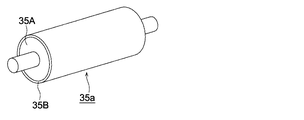
図4は、図3に示したロール回転電極の導電性の金属質母材とその上に被覆されている誘電体の構造の一例を示す斜視図である。 FIG. 4 is a perspective view showing an example of the structure of the conductive metallic base material of the roll rotating electrode shown in FIG. 3 and the dielectric material coated thereon.
図4において、ロール電極35aは導電性の金属質母材35Aとその上に誘電体35Bが被覆されたものである。プラズマ放電処理中の電極表面温度を制御するため、温度調節用の媒体(水もしくはシリコンオイル等)が循環できる構造となっている。
In FIG. 4, a
図5は、角筒型電極の導電性の金属質母材とその上に被覆されている誘電体の構造の一例を示す斜視図である。 FIG. 5 is a perspective view showing an example of the structure of a conductive metallic base material of a rectangular tube electrode and a dielectric material coated thereon.
図5において、角筒型電極36aは、導電性の金属質母材36Aに対し、図4同様の誘電体36Bの被覆を有しており、該電極の構造は金属質のパイプになっていて、それがジャケットとなり、放電中の温度調節が行えるようになっている。
In FIG. 5, a rectangular
なお、角筒型固定電極の数は、上記ロール電極の円周より大きな円周上に沿って複数本設置されていおり、該電極の放電面積はロール回転電極35に対向している全角筒型固定電極面の面積の和で表される。
In addition, the number of the rectangular tube-shaped fixed electrodes is set in plural along the circumference larger than the circumference of the roll electrode, and the discharge area of the electrodes is a full square tube type facing the
図5に示した角筒型電極36aは、円筒型電極でもよいが、角筒型電極は円筒型電極に比べて、放電範囲(放電面積)を広げる効果があるので、本発明に好ましく用いられる。
The
図4及び5において、ロール電極35a及び角筒型電極36aは、それぞれ導電性の金属質母材35A及び36Aの上に誘電体35B及び36Bとしてのセラミックスを溶射後、無機化合物の封孔材料を用いて封孔処理したものである。セラミックス誘電体は片肉で1mm程度被覆あればよい。溶射に用いるセラミックス材としては、アルミナ・窒化珪素等が好ましく用いられるが、この中でもアルミナが加工し易いので、特に好ましく用いられる。また、誘電体層が、ライニングにより無機材料を設けたライニング処理誘電体であってもよい。
4 and 5, a
導電性の金属質母材35A及び36Aとしては、チタン金属またはチタン合金、銀、白金、ステンレススティール、アルミニウム、鉄等の金属等や、鉄とセラミックスとの複合材料またはアルミニウムとセラミックスとの複合材料を挙げることが出来るが、後述の理由からはチタン金属またはチタン合金が特に好ましい。
Examples of the conductive
対向する第1電極および第2の電極の電極間距離は、電極の一方に誘電体を設けた場合、該誘電体表面ともう一方の電極の導電性の金属質母材表面との最短距離のことを言う。双方の電極に誘電体を設けた場合、誘電体表面同士の距離の最短距離のことを言う。電極間距離は、導電性の金属質母材に設けた誘電体の厚さ、印加電界強度の大きさ、プラズマを利用する目的等を考慮して決定されるが、いずれの場合も均一な放電を行う観点から0.1〜20mmが好ましく、特に好ましくは0.5〜2mmである。 When the dielectric is provided on one of the electrodes, the distance between the opposing first electrode and second electrode is the shortest distance between the surface of the dielectric and the surface of the conductive metal base material of the other electrode. Say that. When a dielectric is provided on both electrodes, it means the shortest distance between the dielectric surfaces. The distance between the electrodes is determined in consideration of the thickness of the dielectric provided on the conductive metallic base material, the magnitude of the applied electric field strength, the purpose of using the plasma, etc. From the viewpoint of performing 0.15 mm, 0.1 to 20 mm is preferable, and 0.5 to 2 mm is particularly preferable.
本発明に有用な導電性の金属質母材及び誘電体についての詳細については後述する。 Details of the conductive metallic base material and dielectric useful in the present invention will be described later.
プラズマ放電処理容器31はパイレックス(R)ガラス製の処理容器等が好ましく用いられるが、電極との絶縁がとれれば金属製を用いることも可能である。
The plasma
例えば、アルミニウムまたは、ステンレススティールのフレームの内面にポリイミド樹脂等を張り付けても良く、該金属フレームにセラミックス溶射を行い絶縁性をとってもよい。 For example, polyimide resin or the like may be attached to the inner surface of an aluminum or stainless steel frame, and the metal frame may be thermally sprayed to obtain insulation.
プラズマ放電処理容器31中、特に平行する両電極の両側面には、外部雰囲気中のガスが流入しやすいため、図1には示されていないが、プラズマ放電処理容器31には、上記のような材質で基材面近くまでを覆うカバーを備えることが好ましい。図6(a)及び(b)に、プラズマ放電処理容器の側面にカバー31Aを設け、電極側面を外部雰囲気から遮断できる構造とした例を示す。前記図3には示されていないが、プラズマ放電処理容器31の電極の両側面側をカバー31Aで覆って、図6(b)に示すように、カバーの内側電極側の両端面に、不活性ガスG″(酸素5体積%以下)を供給して(供給路は省略してある)、外部雰囲気がプラズマ処理空間に入り込まないようにする。31Bはプラズマ放電処理容器端部に設けられた不活性ガスの供給口である。これによりプラズマ処理空間周囲は不活性ガスにより外部の雰囲気から遮断される。
Since the gas in the external atmosphere tends to flow into the plasma
本発明の大気圧プラズマ放電処理装置に設置する第1電源(高周波電源)としては、
印加電源記号 メーカー 周波数 製品名
A1 神鋼電機 3kHz SPG3−4500
A2 神鋼電機 5kHz SPG5−4500
A3 春日電機 15kHz AGI−023
A4 神鋼電機 50kHz SPG50−4500
A5 ハイデン研究所 100kHz* PHF−6k
A6 パール工業 200kHz CF−2000−200k
A7 パール工業 400kHz CF−2000−400k
等の市販のものを挙げることが出来、何れも使用することが出来る。
As the first power source (high frequency power source) installed in the atmospheric pressure plasma discharge processing apparatus of the present invention,
Applied power symbol Manufacturer Frequency Product name A1 Shinko Electric 3kHz SPG3-4500
A2 Shinko Electric 5kHz SPG5-4500
A3 Kasuga Electric 15kHz AGI-023
A4 Shinko Electric 50kHz SPG50-4500
A5 HEIDEN Research Laboratories 100kHz * PHF-6k
A6 Pearl Industry 200kHz CF-2000-200k
A7 Pearl Industry 400kHz CF-2000-400k
And the like, and any of them can be used.
また、第2電源(高周波電源)としては、
印加電源記号 メーカー 周波数 製品名
B1 パール工業 800kHz CF−2000−800k
B2 パール工業 2MHz CF−2000−2M
B3 パール工業 13.56MHz CF−5000−13M
B4 パール工業 27MHz CF−2000−27M
B5 パール工業 150MHz CF−2000−150M
等の市販のものを挙げることが出来、何れも好ましく使用出来る。
なお、上記電源のうち、*印はハイデン研究所インパルス高周波電源(連続モードで100kHz)である。それ以外は連続サイン波のみ印加可能な高周波電源である。
As the second power source (high frequency power source),
Applied power supply symbol Manufacturer Frequency Product name B1 Pearl Industry 800kHz CF-2000-800k
B2 Pearl Industry 2MHz CF-2000-2M
B3 Pearl Industry 13.56MHz CF-5000-13M
B4 Pearl Industry 27MHz CF-2000-27M
B5 Pearl Industry 150MHz CF-2000-150M
And the like, and any of them can be preferably used.
Of the above power supplies, * indicates a HEIDEN Laboratory impulse high-frequency power supply (100 kHz in continuous mode). Other than that, it is a high-frequency power source that can apply only a continuous sine wave.
本発明においては、このような電界を印加して、均一で安定な放電状態を保つことが出来る電極を大気圧プラズマ放電処理装置に採用することが好ましい。 In the present invention, it is preferable to employ an electrode capable of maintaining a uniform and stable discharge state by applying such an electric field in an atmospheric pressure plasma discharge treatment apparatus.
本発明において、対向する電極間に印加する電力は、第2電極(第2の高周波電界)に1W/cm2以上の電力(出力密度)を供給し、放電ガスを励起してプラズマを発生させ、エネルギーを薄膜形成ガスに与え、薄膜を形成する。第2電極に供給する電力の上限値としては、好ましくは50W/cm2、より好ましくは20W/cm2である。下限値は、好ましくは1W/cm2、より好ましくは1.2W/cm2である。なお、放電面積(cm2)は、電極において放電が起こる範囲の面積のことを指す。 In the present invention, the electric power applied between the electrodes facing each other supplies power (power density) of 1 W / cm 2 or more to the second electrode (second high-frequency electric field) to excite the discharge gas to generate plasma. The energy is applied to the thin film forming gas to form a thin film. The upper limit value of the power supplied to the second electrode is preferably 50 W / cm 2 , more preferably 20 W / cm 2 . The lower limit is preferably 1W / cm 2, more preferably 1.2 W / cm 2. The discharge area (cm 2 ) refers to an area in a range where discharge occurs in the electrode.
また、第1電極(第1の高周波電界)にも、1W/cm2以上の電力(出力密度)を供給することにより、第2の高周波電界の均一性を維持したまま、出力密度を向上させることが出来る。これにより、更なる均一高密度プラズマを生成出来、更なる製膜速度の向上と膜質の向上が両立出来る。好ましくは5W/cm2以上である。第1電極に供給する電力の上限値は、好ましくは50W/cm2である。 Further, by supplying power (output density) of 1 W / cm 2 or more to the first electrode (first high frequency electric field), the output density is improved while maintaining the uniformity of the second high frequency electric field. I can do it. Thereby, a further uniform high-density plasma can be generated, and a further improvement in film forming speed and an improvement in film quality can be achieved. Preferably it is 5 W / cm 2 or more. The upper limit value of the power supplied to the first electrode is preferably 50 W / cm 2 .
ここで高周波電界の波形としては、特に限定されない。連続モードと呼ばれる連続サイン波状の連続発振モードと、パルスモードと呼ばれるON/OFFを断続的に行う断続発振モード等があり、そのどちらを採用してもよいが、少なくとも第2電極側(第2の高周波電界)は連続サイン波の方がより緻密で良質な膜が得られるので好ましい。 Here, the waveform of the high-frequency electric field is not particularly limited. There are a continuous sine wave continuous oscillation mode called a continuous mode, an intermittent oscillation mode called ON / OFF intermittently called a pulse mode, and either of them may be adopted, but at least the second electrode side (second The high-frequency electric field is preferably a continuous sine wave because a denser and better quality film can be obtained.
このような大気圧プラズマによる薄膜形成法に使用する電極は、構造的にも、性能的にも過酷な条件に耐えられるものでなければならない。このような電極としては、金属質母材上に誘電体を被覆したものであることが好ましい。 An electrode used in such a method for forming a thin film by atmospheric pressure plasma must be able to withstand severe conditions in terms of structure and performance. Such an electrode is preferably a metal base material coated with a dielectric.
本発明に使用する誘電体被覆電極においては、様々な金属質母材と誘電体との間に特性が合うものが好ましく、その一つの特性として、金属質母材と誘電体との線熱膨張係数の差が10×10-6/℃以下となる組み合わせのものである。好ましくは8×10-6/℃以下、更に好ましくは5×10-6/℃以下、更に好ましくは2×10-6/℃以下である。なお、線熱膨張係数とは、周知の材料特有の物性値である。 In the dielectric-coated electrode used in the present invention, it is preferable that the characteristics match between various metallic base materials and dielectrics. One of the characteristics is linear thermal expansion between the metallic base material and the dielectric. The combination is such that the difference in coefficient is 10 × 10 −6 / ° C. or less. It is preferably 8 × 10 −6 / ° C. or less, more preferably 5 × 10 −6 / ° C. or less, and further preferably 2 × 10 −6 / ° C. or less. The linear thermal expansion coefficient is a well-known physical property value of a material.
線熱膨張係数の差が、この範囲にある導電性の金属質母材と誘電体との組み合わせとしては、
1.金属質母材が純チタンまたはチタン合金で、誘電体がセラミックス溶射被膜
2.金属質母材が純チタンまたはチタン合金で、誘電体がガラスライニング
3.金属質母材がステンレススティールで、誘電体がセラミックス溶射被膜
4.金属質母材がステンレススティールで、誘電体がガラスライニング
5.金属質母材がセラミックスおよび鉄の複合材料で、誘電体がセラミックス溶射被膜
6.金属質母材がセラミックスおよび鉄の複合材料で、誘電体がガラスライニング
7.金属質母材がセラミックスおよびアルミの複合材料で、誘電体がセラミックス溶射皮膜
8.金属質母材がセラミックスおよびアルミの複合材料で、誘電体がガラスライニング
等がある。線熱膨張係数の差という観点では、上記1.または2.および5.〜8.が好ましく、特に1.が好ましい。
As a combination of a conductive metallic base material and a dielectric whose difference in linear thermal expansion coefficient is within this range,
1. 1. Metal base material is pure titanium or titanium alloy, and dielectric is ceramic spray coating. 2. Metal base material is pure titanium or titanium alloy, and dielectric is glass lining. 3. Metal base material is stainless steel and dielectric is ceramic sprayed coating. 4. Metal base material is stainless steel and dielectric is glass lining. 5. The metal base material is a composite material of ceramics and iron, and the dielectric is a ceramic spray coating. 6. Metal base material is a composite material of ceramics and iron, and dielectric is glass lining 7. The metal base material is a composite material of ceramics and aluminum, and the dielectric is a ceramic spray coating. The metal base material is a composite material of ceramics and aluminum, and the dielectric is glass lining. From the viewpoint of the difference in coefficient of linear thermal expansion, the above 1. Or 2. And 5. ~ 8. In particular, Is preferred.
本発明において、金属質母材は、上記の特性からはチタンまたはチタン合金が特に有用である。金属質母材をチタンまたはチタン合金とすることにより、誘電体を上記とすることにより、使用中の電極の劣化、特にひび割れ、剥がれ、脱落等がなく、過酷な条件での長時間の使用に耐えることが出来る。 In the present invention, titanium or a titanium alloy is particularly useful as the metallic base material from the above characteristics. By using titanium or a titanium alloy as the metal base material, the dielectric is used as described above, so that there is no deterioration of the electrode in use, especially cracking, peeling, dropping off, etc., and it can be used for a long time under harsh conditions. Can withstand.
本発明に有用な電極の金属質母材は、チタンを70質量%以上含有するチタン合金またはチタン金属である。本発明において、チタン合金またはチタン金属中のチタンの含有量は、70質量%以上であれば、問題なく使用出来るが、好ましくは80質量%以上のチタンを含有しているものが好ましい。本発明に有用なチタン合金またはチタン金属は、工業用純チタン、耐食性チタン、高力チタン等として一般に使用されているものを用いることが出来る。工業用純チタンとしては、TIA、TIB、TIC、TID等を挙げることが出来、何れも鉄原子、炭素原子、窒素原子、酸素原子、水素原子等を極僅か含有しているもので、チタンの含有量としては、99質量%以上を有している。耐食性チタン合金としては、T15PBを好ましく用いることが出来、上記含有原子の他に鉛を含有しており、チタン含有量としては、98質量%以上である。また、チタン合金としては、鉛を除く上記の原子の他に、アルミニウムを含有し、その他バナジウムや錫を含有しているT64、T325、T525、TA3等を好ましく用いることが出来、これらのチタン含有量としては、85質量%以上を含有しているものである。これらのチタン合金またはチタン金属はステンレススティール、例えばAISI316に比べて、熱膨張係数が1/2程度小さく、金属質母材としてチタン合金またはチタン金属の上に施された後述の誘電体との組み合わせがよく、高温、長時間での使用に耐えることが出来る。 The metallic base material of the electrode useful in the present invention is a titanium alloy or titanium metal containing 70% by mass or more of titanium. In the present invention, if the titanium content in the titanium alloy or titanium metal is 70% by mass or more, it can be used without any problem, but preferably contains 80% by mass or more of titanium. As the titanium alloy or titanium metal useful in the present invention, those generally used as industrial pure titanium, corrosion resistant titanium, high strength titanium and the like can be used. Examples of pure titanium for industrial use include TIA, TIB, TIC, TID, etc., all of which contain very little iron atom, carbon atom, nitrogen atom, oxygen atom, hydrogen atom, etc. As content, it has 99 mass% or more. As the corrosion-resistant titanium alloy, T15PB can be preferably used, and it contains lead in addition to the above-mentioned atoms, and the titanium content is 98% by mass or more. Further, as the titanium alloy, T64, T325, T525, TA3, etc. containing aluminum and vanadium or tin in addition to the above atoms except lead can be preferably used. As a quantity, it contains 85 mass% or more. These titanium alloys or titanium metals have a thermal expansion coefficient that is about 1/2 smaller than that of stainless steel, such as AISI 316, and are combined with a dielectric described later applied on the titanium alloy or titanium metal as a metallic base material. It can withstand the use at high temperature for a long time.
一方、誘電体の求められる特性としては、具体的には、比誘電率が6〜45の無機化合物であることが好ましく、また、このような誘電体としては、アルミナ、窒化珪素等のセラミックス、あるいは、ケイ酸塩系ガラス、ホウ酸塩系ガラス等のガラスライニング材等がある。この中では、後述のセラミックスを溶射したものやガラスライニングにより設けたものが好ましい。特にアルミナを溶射して設けた誘電体が好ましい。 On the other hand, as a required characteristic of the dielectric, specifically, an inorganic compound having a relative dielectric constant of 6 to 45 is preferable, and examples of such a dielectric include ceramics such as alumina and silicon nitride, Alternatively, there are glass lining materials such as silicate glass and borate glass. In this, what sprayed the ceramics mentioned later and the thing provided by glass lining are preferable. In particular, a dielectric provided by spraying alumina is preferable.
または、上述のような大電力に耐える仕様の一つとして、誘電体の空隙率が10体積%以下、好ましくは8体積%以下であることで、好ましくは0体積%を越えて5体積%以下である。なお、誘電体の空隙率は、BET吸着法や水銀ポロシメーターにより測定することが出来る。後述の実施例においては、島津製作所製の水銀ポロシメーターにより金属質母材に被覆された誘電体の破片を用い、空隙率を測定する。誘電体が、低い空隙率を有することにより、高耐久性が達成される。このような空隙を有しつつも空隙率が低い誘電体としては、後述の大気プラズマ溶射法等による高密度、高密着のセラミックス溶射被膜等を挙げることが出来る。更に空隙率を下げるためには、封孔処理を行うことが好ましい。 Alternatively, as one of the specifications that can withstand high power as described above, the porosity of the dielectric is 10% by volume or less, preferably 8% by volume or less, preferably more than 0% by volume and 5% by volume or less. It is. The porosity of the dielectric can be measured by a BET adsorption method or a mercury porosimeter. In the examples described later, the porosity is measured using a dielectric fragment covered with a metallic base material by a mercury porosimeter manufactured by Shimadzu Corporation. High durability is achieved because the dielectric has a low porosity. Examples of the dielectric having such a void and a low void ratio include a high-density, high-adhesion ceramic spray coating by an atmospheric plasma spraying method described later. In order to further reduce the porosity, it is preferable to perform sealing treatment.
上記、大気プラズマ溶射法は、セラミックス等の微粉末、ワイヤ等をプラズマ熱源中に投入し、溶融または半溶融状態の微粒子として被覆対象の金属質母材に吹き付け、皮膜を形成させる技術である。プラズマ熱源とは、分子ガスを高温にし、原子に解離させ、更にエネルギーを与えて電子を放出させた高温のプラズマガスである。このプラズマガスの噴射速度は大きく、従来のアーク溶射やフレーム溶射に比べて、溶射材料が高速で金属質母材に衝突するため、密着強度が高く、高密度な被膜を得ることが出来る。詳しくは、特開2000−301655に記載の高温被曝部材に熱遮蔽皮膜を形成する溶射方法を参照することが出来る。この方法により、上記のような被覆する誘電体(セラミック溶射膜)の空隙率にすることが出来る。 The above-mentioned atmospheric plasma spraying method is a technique in which fine powder such as ceramics, wire, or the like is put into a plasma heat source and sprayed onto a metallic base material to be coated as fine particles in a molten or semi-molten state to form a film. A plasma heat source is a high-temperature plasma gas in which a molecular gas is heated to a high temperature, dissociated into atoms, and further given energy to release electrons. The plasma gas injection speed is high, and since the sprayed material collides with the metallic base material at a higher speed than conventional arc spraying or flame spraying, high adhesion strength and high density coating can be obtained. Specifically, reference can be made to a thermal spraying method for forming a heat shielding film on a high-temperature exposed member described in JP-A-2000-301655. By this method, the porosity of the dielectric (ceramic sprayed film) to be coated can be obtained.
また、大電力に耐える別の好ましい仕様としては、誘電体の厚みが0.5〜2mmであることである。この膜厚変動は、5%以下であることが望ましく、好ましくは3%以下、更に好ましくは1%以下である。 Another preferable specification that can withstand high power is that the dielectric thickness is 0.5 to 2 mm. The film thickness variation is desirably 5% or less, preferably 3% or less, and more preferably 1% or less.
誘電体の空隙率をより低減させるためには、上記のようにセラミックス等の溶射膜に、更に、無機化合物で封孔処理を行うことが好ましい。前記無機化合物としては、金属酸化物が好ましく、この中では特に酸化ケイ素(SiOx)を主成分として含有するものが好ましい。 In order to further reduce the porosity of the dielectric, it is preferable to further perform a sealing treatment with an inorganic compound on the sprayed film such as ceramics as described above. As the inorganic compound, a metal oxide is preferable, and among these, a compound containing silicon oxide (SiO x ) as a main component is particularly preferable.
封孔処理の無機化合物は、ゾルゲル反応により硬化して形成したものであることが好ましい。封孔処理の無機化合物が金属酸化物を主成分とするものである場合には、金属アルコキシド等を封孔液として前記セラミック溶射膜上に塗布し、ゾルゲル反応により硬化する。無機化合物がシリカを主成分とするものの場合には、アルコキシシランを封孔液として用いることが好ましい。 The inorganic compound for sealing treatment is preferably formed by curing by a sol-gel reaction. In the case where the inorganic compound for sealing treatment contains a metal oxide as a main component, a metal alkoxide or the like is applied as a sealing liquid on the ceramic sprayed film and cured by a sol-gel reaction. When the inorganic compound is mainly composed of silica, it is preferable to use alkoxysilane as the sealing liquid.
ここでゾルゲル反応の促進には、エネルギー処理を用いることが好ましい。エネルギー処理としては、熱硬化(好ましくは200℃以下)や、紫外線照射などがある。更に封孔処理の仕方として、封孔液を希釈し、コーティングと硬化を逐次で数回繰り返すと、よりいっそう無機質化が向上し、劣化の無い緻密な電極が出来る。 Here, it is preferable to use energy treatment for promoting the sol-gel reaction. Examples of the energy treatment include thermal curing (preferably 200 ° C. or less) and ultraviolet irradiation. Further, when the sealing liquid is diluted as the method of sealing treatment and coating and curing are repeated several times in succession, the mineralization is further improved and a dense electrode without deterioration can be obtained.
本発明に係る誘電体被覆電極の金属アルコキシド等を封孔液として、セラミックス溶射膜にコーティングした後、ゾルゲル反応で硬化する封孔処理を行う場合、硬化した後の金属酸化物の含有量は60モル%以上であることが好ましい。封孔液の金属アルコキシドとしてアルコキシシランを用いた場合には、硬化後のSiOx(xは2以下)含有量が60モル%以上であることが好ましい。硬化後のSiOx含有量は、XPS(X線光電子分光法)により誘電体層の断層を分析することにより測定する。 In the case of performing a sealing treatment that cures by a sol-gel reaction after coating a ceramic sprayed film using the metal alkoxide or the like of the dielectric-coated electrode according to the present invention as a sealing liquid, the content of the metal oxide after curing is 60 It is preferably at least mol%. When alkoxysilane is used as the metal alkoxide of the sealing liquid, the content of SiO x (x is 2 or less) after curing is preferably 60 mol% or more. The cured SiO x content is measured by analyzing a tomographic layer of the dielectric layer by XPS (X-ray photoelectron spectroscopy).
本発明の薄膜形成方法に係る電極においては、電極の少なくとも基材と接する側のJIS B 0601で規定される表面粗さの最大高さ(Rmax)が10μm以下になるように調整することが、本発明に記載の効果を得る観点から好ましいが、更に好ましくは、表面粗さの最大値が8μm以下であり、特に好ましくは、7μm以下に調整することである。このように誘電体被覆電極の誘電体表面を研磨仕上げする等の方法により、誘電体の厚み及び電極間のギャップを一定に保つことが出来、放電状態を安定化出来ること、更に熱収縮差や残留応力による歪やひび割れを無くし、且つ、高精度で、耐久性を大きく向上させることが出来る。誘電体表面の研磨仕上げは、少なくとも基材と接する側の誘電体において行われることが好ましい。更にJIS B 0601で規定される中心線平均表面粗さ(Ra)は0.5μm以下が好ましく、更に好ましくは0.1μm以下である。 In the electrode according to the thin film forming method of the present invention, the maximum height (Rmax) of the surface roughness defined by JIS B 0601 on the side in contact with at least the substrate of the electrode is adjusted to be 10 μm or less. Although it is preferable from the viewpoint of obtaining the effects described in the present invention, the maximum value of the surface roughness is more preferably 8 μm or less, and particularly preferably 7 μm or less. In this way, the dielectric surface of the dielectric-coated electrode can be polished and the dielectric thickness and the gap between the electrodes can be kept constant, the discharge state can be stabilized, the heat shrinkage difference and Distortion and cracking due to residual stress can be eliminated, and durability can be greatly improved with high accuracy. The polishing finish of the dielectric surface is preferably performed at least on the dielectric in contact with the substrate. Furthermore, the centerline average surface roughness (Ra) defined by JIS B 0601 is preferably 0.5 μm or less, more preferably 0.1 μm or less.
本発明に使用する誘電体被覆電極において、大電力に耐える他の好ましい仕様としては、耐熱温度が100℃以上であることである。更に好ましくは120℃以上、特に好ましくは150℃以上である。また上限は500℃である。なお、耐熱温度とは、大気圧プラズマ処理で用いられる電圧において絶縁破壊が発生せず、正常に放電出来る状態において耐えられる最も高い温度のことを指す。このような耐熱温度は、上記のセラミックス溶射や、泡混入量の異なる層状のガラスライニングで設けた誘電体を適用したり、上記金属質母材と誘電体の線熱膨張係数の差の範囲内の材料を適宜選択する手段を適宜組み合わせることによって達成可能である。 In the dielectric-coated electrode used in the present invention, another preferred specification that can withstand high power is that the heat-resistant temperature is 100 ° C. or higher. More preferably, it is 120 degreeC or more, Most preferably, it is 150 degreeC or more. The upper limit is 500 ° C. Note that the heat-resistant temperature refers to the highest temperature that can withstand normal discharge without causing dielectric breakdown at the voltage used in the atmospheric pressure plasma treatment. Such heat-resistant temperature can be applied within the range of the difference between the linear thermal expansion coefficient of the metallic base material and the dielectric material by applying the dielectric material provided by the above-mentioned ceramic spraying or layered glass lining with different bubble mixing amounts. This can be achieved by appropriately combining means for appropriately selecting the materials.
次に、本発明の導電膜形成方法に用いられる反応性ガスについて説明する。本発明の透明導電膜形成方法を実施するにあたり、使用する反応性ガスは、反応性ガス成分として、分子内に少なくとも1つの酸素原子を有する無機ガスと薄膜形成ガスである有機金属化合物からなり、本発明においては、窒素ガスを主体とする不活性ガスとの混合ガスとして用いられる。 Next, the reactive gas used for the electrically conductive film formation method of this invention is demonstrated. In carrying out the transparent conductive film forming method of the present invention, the reactive gas used is composed of an inorganic gas having at least one oxygen atom in the molecule and an organometallic compound as a thin film forming gas as reactive gas components, In the present invention, it is used as a mixed gas with an inert gas mainly composed of nitrogen gas.
反応性ガスは、放電空間でプラズマ状態となり、導電膜を形成する。 The reactive gas becomes a plasma state in the discharge space and forms a conductive film.
本発明において、反応性ガス中には、分子内に少なくとも1つの酸素原子を有する無機ガスが混合されることが好ましく、この例としては、酸素、二酸化炭素、一酸化炭素、一酸化二窒素、二酸化窒素、一酸化硫黄、二酸化硫黄、オゾン等が挙げられ、特に好ましい無機ガスは二酸化窒素である。またこれらのガスを窒素、ヘリウム、アルゴンから選ばれる気体と混合した混合ガスとして使用してもよく、二酸化窒素と窒素の混合ガス等も好ましい。 In the present invention, the reactive gas is preferably mixed with an inorganic gas having at least one oxygen atom in the molecule. Examples of this include oxygen, carbon dioxide, carbon monoxide, dinitrogen monoxide, Nitrogen dioxide, sulfur monoxide, sulfur dioxide, ozone and the like can be mentioned, and a particularly preferred inorganic gas is nitrogen dioxide. These gases may be used as a mixed gas mixed with a gas selected from nitrogen, helium, and argon, and a mixed gas of nitrogen dioxide and nitrogen is also preferable.
これらのガスは混合ガスに対して、0.0001〜5.0体積%の範囲で用いることができるが、好ましい範囲は、0.001〜3.0体積%である。 These gases can be used in a range of 0.0001 to 5.0% by volume with respect to the mixed gas, but a preferable range is 0.001 to 3.0% by volume.
放電ガスは、薄膜形成可能なグロー放電を起こすことの出来るガスであり、それ自身がエネルギーを授受する媒体として働く。放電ガスとしては、窒素、希ガス、空気などがあり、これらを単独で放電ガスとして用いても、混合して用いてもかまわない。本発明において、放電ガスとして好ましいのは窒素であり、放電ガスの50〜100体積%が窒素ガスでを含有するものである。また、窒素以外の放電ガスとしては、希ガスを50体積%未満含有してもよい。希ガスとしては、周期表の第18属元素、具体的には、ヘリウム、ネオン、アルゴン、クリプトン、キセノン、ラドン等を挙げることが出来る。また、放電ガスの量は、放電空間または処理空間に供給する全ガス量に対し、90〜99.9体積%含有することが好ましい。
The discharge gas is a gas capable of causing a glow discharge capable of forming a thin film, and itself functions as a medium for transferring energy. Examples of the discharge gas include nitrogen, rare gas, air, and the like. These may be used alone as a discharge gas or may be used in combination. In the present invention, nitrogen is preferable as the discharge gas, and 50 to 100% by volume of the discharge gas contains nitrogen gas. Moreover, as discharge gas other than nitrogen, you may contain rare gas less than 50 volume%. Examples of the rare gas include
透明導電膜形成ガスとは、放電ガスからのエネルギーを受け取って、それ自身は励起して活性(プラズマ状態)となり、基材上に化学的に堆積して透明導電膜を形成する原料のことである。 The transparent conductive film forming gas is a raw material that receives energy from the discharge gas and is excited to become active (plasma state) and is chemically deposited on the substrate to form the transparent conductive film. is there.
本発明に使用する透明導電膜形成ガスについて説明する。 The transparent conductive film forming gas used in the present invention will be described.
本発明に使用する透明導電膜形成ガスとしては、有機金属化合物、ハロゲン金属化合物、金属水素化合物等を挙げることが出来る。 Examples of the transparent conductive film forming gas used in the present invention include organic metal compounds, halogen metal compounds, metal hydrogen compounds, and the like.
本発明においては、透明導電膜形成ガスは有機金属化合物を含有していることが好ましく、また有機金属化合物から形成される金属酸化物にドーピングするドーピング用有機金属化合物を加える場合があり、同様な有機金属化合物が使用される。 In the present invention, the transparent conductive film-forming gas preferably contains an organometallic compound, and an organometallic compound for doping may be added to the metal oxide formed from the organometallic compound. Organometallic compounds are used.
本発明に有用な有機金属化合物は下記の一般式(I)で示すものが好ましい。 The organometallic compounds useful in the present invention are preferably those represented by the following general formula (I).
一般式(I) R1 xMR2 yR3 z
式中、Mは金属、R1はアルキル基、R2はアルコキシ基、R3はβ−ジケトン配位基、β−ケトカルボン酸エステル配位基、β−ケトカルボン酸配位基及びケトオキシ基(ケトオキシ配位基)から選ばれる基であり、金属Mの価数をmとした場合、x+y+z=mであり、x=0〜m、またはx=0〜m−1であり、y=0〜m、z=0〜mで、何れも0または正の整数である。R1のアルキル基としては、メチル基、エチル基、プロピル基、ブチル基等を挙げることが出来る。R2のアルコキシ基としては、例えばメトキシ基、エトキシ基、プロポキシ基、ブトキシ基、3,3,3−トリフルオロプロポキシ基等を挙げることが出来る。またアルキル基の水素原子をフッ素原子に置換したものでもよい。R3のβ−ジケトン配位基、β−ケトカルボン酸エステル配位基、β−ケトカルボン酸配位基及びケトオキシ基(ケトオキシ配位基)から選ばれる基としては、β−ジケトン配位基として、例えば、2,4−ペンタンジオン(アセチルアセトンあるいはアセトアセトンともいう)、1,1,1,5,5,5−ヘキサメチル−2,4−ペンタンジオン、2,2,6,6−テトラメチル−3,5−ヘプタンジオン、1,1,1−トリフルオロ−2,4−ペンタンジオン等を挙げることが出来、β−ケトカルボン酸エステル配位基として、例えば、アセト酢酸メチルエステル、アセト酢酸エチルエステル、アセト酢酸プロピルエステル、トリメチルアセト酢酸エチル、トリフルオロアセト酢酸メチル等を挙げることが出来、β−ケトカルボン酸として、例えば、アセト酢酸、トリメチルアセト酢酸等を挙げることが出来、またケトオキシとして、例えば、アセトオキシ基(またはアセトキシ基)、プロピオニルオキシ基、ブチリロキシ基、アクリロイルオキシ基、メタクリロイルオキシ基等を挙げることが出来る。これらの基の炭素原子数は、上記例有機金属示化合物を含んで、18以下が好ましい。また例示にもあるように直鎖または分岐のもの、また水素原子をフッ素原子に置換したものでもよい。
Formula (I) R 1 x MR 2 y R 3 z
In the formula, M is a metal, R 1 is an alkyl group, R 2 is an alkoxy group, R 3 is a β-diketone coordination group, a β-ketocarboxylic acid ester coordination group, a β-ketocarboxylic acid coordination group, and a ketooxy group (ketooxy group). A coordination group), where the valence of the metal M is m, x + y + z = m, x = 0 to m, or x = 0 to m-1, and y = 0 to m. , Z = 0 to m, and each is 0 or a positive integer. Examples of the alkyl group for R 1 include a methyl group, an ethyl group, a propyl group, and a butyl group. Examples of the alkoxy group for R 2 include a methoxy group, an ethoxy group, a propoxy group, a butoxy group, and a 3,3,3-trifluoropropoxy group. Further, a hydrogen atom in the alkyl group may be substituted with a fluorine atom. As a group selected from a β-diketone coordination group, a β-ketocarboxylic acid ester coordination group, a β-ketocarboxylic acid coordination group and a ketooxy group (ketooxy coordination group) of R 3 , as a β-diketone coordination group, For example, 2,4-pentanedione (also referred to as acetylacetone or acetoacetone), 1,1,1,5,5,5-hexamethyl-2,4-pentanedione, 2,2,6,6-tetramethyl-3 , 5-heptanedione, 1,1,1-trifluoro-2,4-pentanedione, etc., and β-ketocarboxylic acid ester coordination groups include, for example, acetoacetic acid methyl ester, acetoacetic acid ethyl ester, Examples include acetoacetic acid propyl ester, trimethylacetoacetic acid ethyl, trifluoroacetoacetic acid methyl, and the like, as β-ketocarboxylic acid, Eg to acetoacetate, it can be mentioned trimethyl acetoacetate, and as Ketookishi, for example, acetoxy group (or an acetoxy group), a propionyloxy group, Buchirirokishi group, acryloyloxy group, methacryloyloxy group and the like. The number of carbon atoms of these groups is preferably 18 or less, including the above-mentioned organometallic compounds. Further, as illustrated, it may be linear or branched, or a hydrogen atom substituted with a fluorine atom.
本発明において取り扱いの問題から、爆発の危険性の少ない有機金属化合物が好ましく、分子内に少なくとも一つ以上の酸素を有する有機金属化合物が好ましい。このようなものとしてR2のアルコキシ基を少なくとも一つを含有する有機金属化合物、またR3のβ−ジケトン配位基、β−ケトカルボン酸エステル配位基、β−ケトカルボン酸配位基及びケトオキシ基(ケトオキシ配位基)から選ばれる基を少なくとも一つ有する金属化合物が好ましい。 In the present invention, an organometallic compound having a low risk of explosion is preferred from the viewpoint of handling, and an organometallic compound having at least one oxygen in the molecule is preferred. As such, an organometallic compound containing at least one alkoxy group of R 2 , a β-diketone coordination group, a β-ketocarboxylic acid ester coordination group, a β-ketocarboxylic acid coordination group and a ketooxy group of R 3 A metal compound having at least one group selected from a group (ketooxy coordination group) is preferred.
本発明に使用し得る有機金属化合物の金属は、特に制限ないが、インジウム(In)、錫(Sn)、亜鉛(Zn)、ジルコニウム(Zr)、アルミニウム(Al)及びアンチモン(Sb)、ガリウム(Ga)、ゲルマニウム(Ge)から選ばれる少なくとも1種の金属が好ましく、インジウム、亜鉛及び錫から選ばれる少なくとも1種の金属が特に好ましい。 The metal of the organometallic compound that can be used in the present invention is not particularly limited, but indium (In), tin (Sn), zinc (Zn), zirconium (Zr), aluminum (Al), antimony (Sb), gallium ( At least one metal selected from Ga) and germanium (Ge) is preferable, and at least one metal selected from indium, zinc and tin is particularly preferable.
この中特に、前記一般式1または2で表される化合物は好ましいものである。
Among these, the compound represented by the
一般式1及び2において、MはIn、Sn、Znを表し、R1、R2はそれぞれ置換基を有していてもよいアルキル基、アリール基、アルコキシル基を表し、Rは水素原子、置換基を表し、また、RはR1、R2と結合して環を形成してもよい。R3はそれぞれ置換基を有していてもよいアルキル基、アリール基を表す。n1は整数を表し、n2は整数を表す。
In
一般式1で表される有機金属化合物を形成する配位子の具体例としては、以下に示す化合物が挙げられる。 Specific examples of the ligand that forms the organometallic compound represented by the general formula 1 include the compounds shown below.
また、下記のジケトン化合物も配位子として好ましい。 The following diketone compounds are also preferred as the ligand.
一般式1及び2におけるMとしてはインジウム(In)が好ましい。本発明の有機化合物の中で好ましい例としては、インジウムヘキサフルオロペンタンジオネート、インジウムメチル(トリメチル)アセチルアセテート、インジウムアセチルアセトナート、インジウムイソポロポキシド、インジウムトリフルオロペンタンジオネート、トリス(2,2,6,6−テトラメチル3,5−ヘプタンジオネート)インジウム、ジ−n−ブチルビス(2,4−ペンタンジオネート)スズ、ジ−n−ブチルジアセトキシスズ、ジ−t−ブチルジアセトキシスズ、テトライソプロポキシスズ、テトラブトキシスズ、ジンクアセチルアセトナート等を挙げることが出来る。この中で特に好ましいのはインジウムアセチルアセトナート、トリス(2,2,6,6−テトラメチル3,5−ヘプタンジオネート)インジウム、ジンクアセチルアセトナート、ジ−n−ブチルジアセトキシスズである。これらの有機金属化合物は一般に市販されており、例えば、インジウムアセチルアセトナートは東京化成工業(株)から容易に入手することができる。
In
本発明において、上記の好ましい有機金属化合物の例としては、インジウムトリス2,4−ペンタンジオナート(あるいは、トリスアセトアセトナートインジウム)、インジウムトリスヘキサフルオロペンタンジオナート、メチルトリメチルアセトキシインジウム、トリアセトアセトオキシインジウム、トリアセトオキシインジウム、ジエトキシアセトアセトオキシインジウム、インジウムトリイソポロポキシド、ジエトキシインジウム(1,1,1−トリフルオロペンタンジオナート)、トリス(2,2,6,6−テトラメチル−3,5−ヘプタンジオナート)インジウム、エトキシインジウムビスアセトメチルアセタート、ジ(n)ブチルビス(2,4−ペンタンジオナート)錫、ジ(n)ブチルジアセトオキシ錫、ジ(t)ブチルジアセトオキシ錫、テトライソプロポキシ錫、テトラ(i)ブトキシ錫、亜鉛2,4−ペンタンジオナート等を挙げることが出来、何れも好ましく用いることが出来る。
In the present invention, examples of the preferable organometallic compound include
この中で特にインジウムトリス2,4−ペンタンジオナート、トリス(2,2,6,6−テトラメチル−3,5−ヘプタンジオナート)インジウム、亜鉛ビス2,4−ペンタンジオナート、ジ(n)ブチルジアセトオキシ錫が好ましい。これらの有機金属化合物は一般に市販(例えば、東京化成工業(株)等から)されている。
Among them,
本発明において、該有機金属化合物から形成される透明導電膜の導電性を更に高めるためのドーピング用有機金属化合物またはドーピング用フッ素化合物を混合ガスに含有させることが好ましい。ドーピング用有機金属化合物またはドーピング用フッ素化合物の透明導電膜形成ガスとしては、例えば、トリイソプロポキシアルミニウム、ニッケルトリス2,4−ペンタンジオナート、マンガンビス2,4−ペンタンジオナート、ボロンイソプロポキシド、トリ(n)ブトキシアンチモン、トリ(n)ブチルアンチモン、ジ(n)ブチル錫ビス2,4−ペンタンジオナート、ジ(n)ブチルジアセトオキシ錫、ジ(t)ブチルジアセトオキシ錫、テトライソプロポキシ錫、テトラブトキシ錫、テトラブチル錫、亜鉛2,4−ペンタンジオナート、ジプロポキシゲルマニウム、ジ(n)ブチルジアセトオキシゲルマニウム、ゲルマニウムトリス2,4−ペンタンジオナート、ガリウムトリス2,4−ペンタンジオナート、トリプロポキシガリウム、ブチルジアセトオキシガリウム、六フッ化プロピレン、八フッ化シクロブタン、四フッ化メタン等を挙げることが出来る。
In the present invention, it is preferable that a mixed gas contains an organic metal compound for doping or a fluorine compound for doping for further enhancing the conductivity of the transparent conductive film formed from the organic metal compound. Examples of the gas for forming a transparent conductive film of an organometallic compound for doping or a fluorine compound for doping include, for example, triisopropoxyaluminum,
前記透明導電膜を形成するに必要な有機金属化合物と上記ドーピング用の透明導電膜形成ガスの比は、形成する透明導電膜の種類により異なるが、例えば、酸化インジウムに錫をドーピングして得られるITO膜においては、In:Snの原子数比が100:0.1〜100:15の範囲になるように透明導電膜形成ガス量を調整することが必要である。好ましくは、100:0.5〜100:10になるよう調整することが好ましい。酸化錫にフッ素をドーピングして得られる透明導電膜(フッ素ドープ酸化錫膜をFTO膜という)においては、得られたFTO膜のSn:Fの原子数比が100:0.01〜100:50の範囲になるよう透明導電膜形成ガスの量比を調整することが好ましい。In2O3−ZnO透明導電膜においては、In:Znの原子数比が100:50〜100:5の範囲になるよう透明導電膜形成ガスの量比を調整することが好ましい。In:Sn、Sn:F及びIn:Znの各原子数比はXPS測定によって求めることが出来る。 The ratio between the organometallic compound necessary for forming the transparent conductive film and the transparent conductive film forming gas for doping differs depending on the type of transparent conductive film to be formed. For example, it can be obtained by doping indium oxide with tin. In the ITO film, it is necessary to adjust the amount of the transparent conductive film forming gas so that the atomic ratio of In: Sn is in the range of 100: 0.1 to 100: 15. Preferably, it is preferable to adjust so that it may become 100: 0.5-100: 10. In a transparent conductive film obtained by doping fluorine into tin oxide (a fluorine-doped tin oxide film is referred to as an FTO film), the obtained FTO film has an Sn: F atomic ratio of 100: 0.01 to 100: 50. It is preferable to adjust the amount ratio of the transparent conductive film forming gas so as to be in the range. In the In 2 O 3 —ZnO transparent conductive film, the amount ratio of the transparent conductive film forming gas is preferably adjusted so that the In: Zn atomic ratio is in the range of 100: 50 to 100: 5. Each atomic ratio of In: Sn, Sn: F and In: Zn can be determined by XPS measurement.
本発明において、得られる透明導電膜は、例えば、SnO2、In2O3(IO)、ZnOの酸化物膜、またはSbドープSnO2、FTO(フッ素ドープSnO2)、AlドープZnO、ZnドープIn、ITO、ATO(ZnドープSnO2)、AZO(AlドープZnO)、IZO(In2O3−ZnO系アモルファス膜)等ドーパントによりドーピングされた複合酸化物を挙げることが出来、これらから選ばれる少なくとも一つを主成分とするアモルファス膜が好ましい。またその他にカルコゲナイド、LaB6、TiN、TiC等の非酸化物膜、Pt、Au、Ag、Cu等の金属膜、CdO等の透明導電膜を挙げることが出来る。 In the present invention, the obtained transparent conductive film is, for example, SnO 2 , In 2 O 3 (IO), an oxide film of ZnO, or Sb-doped SnO 2 , FTO (fluorine-doped SnO 2 ), Al-doped ZnO, Zn-doped. A composite oxide doped with a dopant such as In, ITO, ATO (Zn-doped SnO 2 ), AZO (Al-doped ZnO), IZO (In 2 O 3 —ZnO-based amorphous film), and the like can be selected. An amorphous film containing at least one as a main component is preferable. Other examples include non-oxide films such as chalcogenide, LaB 6 , TiN, and TiC, metal films such as Pt, Au, Ag, and Cu, and transparent conductive films such as CdO.
上記、有機金属化合物の透明導電膜形成ガスは全ガス中で0.01〜10体積%含有されることが好ましく、より好ましくは0.1〜3体積%である。 The gas for forming a transparent conductive film of an organometallic compound is preferably contained in an amount of 0.01 to 10% by volume, more preferably 0.1 to 3% by volume in the total gas.
本発明で用いるガスには分子内に少なくとも1つの酸素原子を有する無機ガスが混合されることが好ましく、これらのガスの量は全ガスに対して、0.0001〜5.0体積%、好ましくは0.001〜3.0体積%である。これらのガスを含有させることにより、透明導電膜中の酸素濃度を調整し、導電性を向上させることが出来る。 The gas used in the present invention is preferably mixed with an inorganic gas having at least one oxygen atom in the molecule, and the amount of these gases is preferably 0.0001 to 5.0% by volume, preferably based on the total gas. Is 0.001 to 3.0% by volume. By containing these gases, the oxygen concentration in the transparent conductive film can be adjusted and the conductivity can be improved.
このようにして形成される透明導電膜の炭素含有量は、2〜0.01atomic%の範囲、また、膜中の窒素含有量は、2〜0.01atomic%の範囲とすることが好ましい。 The carbon content of the transparent conductive film thus formed is preferably in the range of 2 to 0.01 atomic%, and the nitrogen content in the film is preferably in the range of 2 to 0.01 atomic%.
形成される透明導電膜は、窒素を50%以上含む放電ガスを用いたほか、酸化性のガスとして二酸化窒素等の酸素原子を含有する無機ガス(例えば二酸化窒素等)を前記の範囲で含有させることで、炭素含有量、および窒素含有量を前記の範囲とすることが出来、好ましい、キャリア密度、キャリア移動度を得ることが出来、透明導電膜の電気伝導率が向上する。炭素、窒素等のコンタミ(不純物成分)がこの範囲を超えて多くなると、混入した炭素、窒素等に由来する成分が、膜中のキャリアをトラップし、キャリア密度、移動度を低下させ、抵抗率を増加させてしまう。 The formed transparent conductive film uses a discharge gas containing 50% or more of nitrogen, and contains an inorganic gas containing oxygen atoms such as nitrogen dioxide (for example, nitrogen dioxide) as the oxidizing gas in the above range. Thereby, carbon content and nitrogen content can be made into the said range, a preferable carrier density and carrier mobility can be obtained, and the electrical conductivity of a transparent conductive film improves. When contamination (impurity components) such as carbon and nitrogen exceeds this range, the components derived from the mixed carbon and nitrogen trap the carriers in the film, lower the carrier density and mobility, and the resistivity. Will increase.
《炭素含有率、窒素含有率の測定》
これら薄膜中の炭素含有率又窒素含有率は、それぞれ膜を形成した段階でそれぞれ、XPS表面分析装置を用いて求めた。用いるXPS表面分析装置は特に限定はなく、如何なる機種も使用することができるが、本発明実施例においては、VGサイエンティフィックス社製ESCALAB−200Rを用いた。測定は、X線アノードにはMgを用い、出力600W(加速電圧15kV、エミッション電流40mA)で行った。エネルギー分解能は、清浄なAg3d5/2ピークの半値幅で規定したとき、1.5〜1.7eVとなるように設定した。
<< Measurement of carbon content and nitrogen content >>
The carbon content or nitrogen content in these thin films was determined using an XPS surface analyzer at the stage where the films were formed. There are no particular limitations on the XPS surface analyzer used, and any model can be used, but in the examples of the present invention, ESCALAB-200R manufactured by VG Scientific was used. The measurement was performed using Mg for the X-ray anode and an output of 600 W (acceleration voltage: 15 kV, emission current: 40 mA). The energy resolution was set to be 1.5 to 1.7 eV when defined by the half width of a clean Ag3d5 / 2 peak.
測定を行う前に、汚染による影響を除くために、薄膜の膜厚の10〜20%の厚さに相当する表面層をエッチング除去した。表面層の除去には、希ガスイオンが利用できるイオン銃を用いることが好ましく、イオン種としては、He、Ne、Ar、Xe、Krなどが利用できる。本測定おいては、Arイオンエッチングを用いて表面層を除去した。 Before the measurement, the surface layer corresponding to 10 to 20% of the thickness of the thin film was removed by etching in order to remove the influence of contamination. For the removal of the surface layer, it is preferable to use an ion gun that can use rare gas ions. As the ion species, He, Ne, Ar, Xe, Kr, or the like can be used. In this measurement, the surface layer was removed using Ar ion etching.
先ず、結合エネルギー0eVから1100eVの範囲を、データ取り込み間隔1.0eVで測定し、いかなる元素が検出されるかを求めた。 First, the range of binding energy from 0 eV to 1100 eV was measured at a data acquisition interval of 1.0 eV to determine what elements were detected.
次に、検出された、エッチングイオン種を除く全ての元素について、データの取り込み間隔を0.2eVとして、その最大強度を与える光電子ピークについてナロースキャンを行い、各元素のスペクトルを測定した。得られたスペクトルは、測定装置、あるいは、コンピューターの違いによる含有率算出結果の違いを生じせしめなくするために、VAMAS−SCA−JAPAN製のCOMMON DATA PROCESSING SYSTEM(Ver.2.3以降が好ましい。)上に転送した後、同ソフトで処理をおこない、炭素、窒素含有率の値を原子数濃度(atomic concentration:at%)として求めた。 Next, with respect to all the detected elements except for the etching ion species, the data capture interval was set to 0.2 eV, and the photoelectron peak giving the maximum intensity was subjected to narrow scan, and the spectrum of each element was measured. The obtained spectrum is preferably COMMON DATA PROCESSING SYSTEM (Ver. 2.3 or later) manufactured by VAMAS-SCA-JAPAN in order not to cause a difference in the content calculation result due to a difference in measuring apparatus or computer. ) After transferring to the above, processing was performed with the same software, and values of carbon and nitrogen content were determined as atomic concentration (at%).
また、錫とインジウムの比も、上記結果から得られた原子数濃度の比として求めることができる。 Further, the ratio of tin to indium can also be obtained as the ratio of the atomic number concentration obtained from the above result.
また、定量処理をおこなう前に、各元素についてCount Scaleのキャリブレーションを行い、5ポイントのスムージング処理を行った。定量処理では、バックグラウンドを除去したピークエリア強度(cps×eV)を用いた。 Further, before performing the quantitative process, the calibration of the Scale for each element was performed, and a 5-point smoothing process was performed. In the quantitative process, the peak area intensity (cps × eV) from which the background was removed was used.
バックグラウンド処理には、Shirley法を用いた。 The Shirley method was used for background processing.
Shirley法については、D.A.Shirley,Phys.Rev.,B5,4709(1972)を参考にすることができる。 For the Shirley method, see D.C. A. Shirley, Phys. Rev. , B5, 4709 (1972).
上記形成される金属酸化物または金属複合化合物の透明導電膜の膜厚は、0.1〜1000nmの範囲が好ましい。 The film thickness of the metal oxide or metal composite compound transparent conductive film formed is preferably in the range of 0.1 to 1000 nm.
本発明の透明導電膜を有する物品の製造方法により得られる透明導電膜は、高いキャリア移動度を有する特徴を持つ。よく知られているように透明導電膜の電気伝導率は以下の(1)式で表される。 The transparent conductive film obtained by the method for producing an article having the transparent conductive film of the present invention has a characteristic of having high carrier mobility. As is well known, the electrical conductivity of the transparent conductive film is represented by the following formula (1).
σ=n×e×μ (1)
ここで、σは電気伝導率、nはキャリア密度、eは電子の電気量、そしてμはキャリアの移動度である。電気伝導率σを上げるためにはキャリア密度nあるいはキャリア移動度μを増大させる必要があるが、キャリア密度nを増大させていくと2×1021cm-3付近から反射率が大きくなるため透明性が失われる。そのため、電気伝導率σを増大させるためにはキャリア移動度μを増大させる必要がある。本発明の透明導電膜の形成方法によれば条件を最適化することにより、DCマグネトロンスパッタリング法により形成された透明導電膜に近いキャリア移動度μを有する透明導電膜を形成することが可能であることが判明した。
σ = n × e × μ (1)
Here, σ is the electric conductivity, n is the carrier density, e is the quantity of electrons, and μ is the carrier mobility. In order to increase the electrical conductivity σ, it is necessary to increase the carrier density n or the carrier mobility μ. However, as the carrier density n is increased, the reflectivity increases from around 2 × 10 21 cm −3 , so that it is transparent. Sex is lost. Therefore, in order to increase the electrical conductivity σ, it is necessary to increase the carrier mobility μ. According to the method for forming a transparent conductive film of the present invention, it is possible to form a transparent conductive film having a carrier mobility μ close to that of a transparent conductive film formed by a DC magnetron sputtering method by optimizing the conditions. It has been found.
市販されているDCマグネトロンスパッタリング法置により作成された透明導電膜のキャリア移動度は30cm2/sec・V程度である。しかし、本発明の導電膜形成方法によれば、条件を最適化することにより市販の装置を用いたDCマグネトロンスパッタリング法により形成された透明導電膜を超えるキャリア移動度を有する透明導電膜を形成することが可能であることが判明した。 The carrier mobility of the transparent conductive film prepared by a commercially available DC magnetron sputtering method is about 30 cm 2 / sec · V. However, according to the conductive film formation method of the present invention, a transparent conductive film having a carrier mobility exceeding that of the transparent conductive film formed by the DC magnetron sputtering method using a commercially available apparatus is formed by optimizing the conditions. It turns out that it is possible.
本発明の導電膜形成方法を用いることにより、キャリア移動度が10cm2/V・sec以上の透明導電膜を得ることができる。 By using the conductive film forming method of the present invention, a transparent conductive film having a carrier mobility of 10 cm 2 / V · sec or more can be obtained.
本発明の透明導電膜の形成方法は高いキャリア移動度μを有するため、ドーピングなしでも比抵抗値として1×10⁻³Ω・cm以下の比抵抗値の透明導電膜を得ることが出来る。ドーピングを行いキャリア密度nを増加させることで更に比抵抗値を下げることが出来る。また、必要に応じて比抵抗値を上げる薄膜形成ガスを用いることにより、比抵抗値として1×10⁻²Ω・cm以上の高比抵抗値の透明導電膜を得ることも出来る。透明導電膜の比抵抗値を調整するために用いる薄膜形成ガスとしては、例えば、チタントリイソプロポキシド、テトラメトキシシラン、テトラエトキシシラン、ヘキサメチルジシロキサン等を挙げることが出来る。 Since the method for forming a transparent conductive film of the present invention has a high carrier mobility μ, a transparent conductive film having a specific resistance value of 1 × 10 −3 Ω · cm or less can be obtained without doping. The specific resistance can be further lowered by doping to increase the carrier density n. In addition, by using a thin film forming gas that increases the specific resistance value as necessary, a transparent conductive film having a high specific resistance value of 1 × 10 −2 Ω · cm or more can be obtained. Examples of the thin film forming gas used for adjusting the specific resistance value of the transparent conductive film include titanium triisopropoxide, tetramethoxysilane, tetraethoxysilane, and hexamethyldisiloxane.
本発明の透明導電膜の形成方法によって得られる透明導電膜は、キャリア密度nが、1×1019cm-3以上、より好ましい条件下においては、1×1020cm-3以上となるが、透明性は低下しない。 The transparent conductive film obtained by the method for forming a transparent conductive film of the present invention has a carrier density n of 1 × 10 19 cm −3 or more, more preferably 1 × 10 20 cm −3 or more under more preferable conditions. Transparency does not decrease.
本発明において、比抵抗値は、JIS−R−1637に従い、四端子法により求める。なお、測定には例えば、三菱化学製ロレスタ−GP、MCP−T600を用いた。 In the present invention, the specific resistance value is determined by a four-terminal method in accordance with JIS-R-1637. In addition, for example, Mitsubishi Chemical Loresta-GP and MCP-T600 were used for the measurement.
また、キャリア密度、移動度については、例えば、三和無線測器研究所M1−675システムを用いてvan der Pauw法にて、測定を行うことで求めることができる。 Further, the carrier density and mobility can be obtained by performing measurement by the van der Pauw method using, for example, the Sanwa Radio Instrument Laboratory M1-675 system.
本発明の優れた効果の一つとして、エッチングがある。各種ディスプレイ素子を電極として用いる場合、基板上に回路を描くパターニング工程は必須なものであり、パターニングが容易に行うことが出来るかが工程適性上重要な課題となっている。一般に、パターニングはフォトリソグラフィー法により行われることが多く、導通を必要としない部分はエッチングにより溶解、除去するため、該部分のエッチング液による溶解の速さ及び残渣のないことが重要な課題となっている。エッチング液には、通常、硝酸、塩酸、塩酸と硝酸の混酸、フッ酸、塩化第二鉄水溶液等が用いられ、これらのウェットエッチングする方法が主流である。 One of the excellent effects of the present invention is etching. When various display elements are used as electrodes, a patterning process for drawing a circuit on a substrate is indispensable, and whether patterning can be easily performed is an important issue in terms of process suitability. In general, patterning is often performed by a photolithography method, and a portion that does not require conduction is dissolved and removed by etching. Therefore, the speed of dissolution of the portion by the etchant and the absence of residue are important issues. ing. As the etching solution, nitric acid, hydrochloric acid, mixed acid of hydrochloric acid and nitric acid, hydrofluoric acid, ferric chloride aqueous solution or the like is usually used, and these wet etching methods are mainstream.
透明性導電性薄膜として、上記形成された酸化物または複合酸化物の薄膜の膜厚は、0.1〜1000nmの範囲が好ましい。 As the transparent conductive thin film, the thickness of the formed oxide or composite oxide thin film is preferably in the range of 0.1 to 1000 nm.
本発明に係わる透明導電膜を形成する基材について説明する。 The base material which forms the transparent conductive film concerning this invention is demonstrated.
本発明に係わる透明導電膜を形成する基材としては、薄膜をその表面に形成出来るものであれば特に限定はない。基材がプラズマ状態の混合ガスに晒され、均一の薄膜が形成されるものであれば基材の形態または材質には制限ない。樹脂フィルム、樹脂シート(板)、ガラス板が本発明には適している。 The substrate for forming the transparent conductive film according to the present invention is not particularly limited as long as a thin film can be formed on the surface thereof. There is no limitation on the form or material of the substrate as long as the substrate is exposed to a plasma mixed gas to form a uniform thin film. Resin films, resin sheets (plates), and glass plates are suitable for the present invention.
本発明の透明導電膜形成方法は、基材表面温度が比較的低い場合においても、高性能の透明導電膜を形成出来るため、基材表面温度300℃以下でプラズマ放電処理することが好ましく、ガラス以外の樹脂フィルム、樹脂シート、樹脂レンズ等の表面に透明導電膜を、比較的低温で材質の変形なく容易に形成することができる。 Since the transparent conductive film forming method of the present invention can form a high-performance transparent conductive film even when the substrate surface temperature is relatively low, it is preferable to perform plasma discharge treatment at a substrate surface temperature of 300 ° C. or less. A transparent conductive film can be easily formed on the surface of other resin films, resin sheets, resin lenses, etc. at a relatively low temperature without deformation of the material.
樹脂フィルムは本発明に係る大気圧プラズマ放電処理装置の電極間または電極の近傍を連続的に移送させて透明導電膜を形成することが出来るので、スパッタリングのような真空系のようなバッチ式でない、大量生産に向き、連続的な生産性の高い生産方式として好適である。 Since the resin film can form a transparent conductive film by continuously transferring between or in the vicinity of the electrodes of the atmospheric pressure plasma discharge processing apparatus according to the present invention, it is not a batch type like a vacuum system such as sputtering. Suitable for mass production, suitable as a continuous and highly productive production method.
樹脂フィルム、樹脂シート、樹脂レンズ、樹脂成形物等成形物の材質としては、セルローストリアセテート、セルロースジアセテート、セルロースアセテートプロピオネートまたはセルロースアセテートブチレートのようなセルロースエステル、ポリエチレンテレフタレートやポリエチレンナフタレートのようなポリエステル、ポリエチレンやポリプロピレンのようなポリオレフィン、ポリ塩化ビニリデン、ポリ塩化ビニル、ポリビニルアルコール、エチレンビニルアルコールコポリマー、シンジオタクティックポリスチレン、ポリカーボネート、ノルボルネン樹脂、ポリメチルペンテン、ポリエーテルケトン、ポリイミド、ポリエーテルスルフォン、ポリスルフォン、ポリエーテルイミド、ポリアミド、フッ素樹脂、ポリメチルアクリレート、アクリレートコポリマー等を挙げることが出来る。 Resin films, resin sheets, resin lenses, resin moldings and other molded materials include cellulose triacetate, cellulose diacetate, cellulose acetate propionate or cellulose acetate such as cellulose acetate butyrate, polyethylene terephthalate and polyethylene naphthalate. Polyester such as Polyethylene, Polyethylene such as Polypropylene, Polypropylene, Polyvinylidene chloride, Polyvinyl chloride, Polyvinyl alcohol, Ethylene vinyl alcohol copolymer, Syndiotactic polystyrene, Polycarbonate, Norbornene resin, Polymethylpentene, Polyetherketone, Polyimide, Polyether Sulfone, polysulfone, polyetherimide, polyamide, fluororesin, polymethylacrylate , It can be mentioned acrylate copolymer and the like.
これらの素材は単独であるいは適宜混合されて使用することも出来る。中でもゼオネックスやゼオノア(日本ゼオン(株)製)、非晶質シクロポリオレフィン樹脂フィルムのARTON(日本合成ゴム(株)製)、ポリカーボネートフィルムのピュアエース(帝人(株)製)、セルローストリアセテートフィルムのコニカタックKC4UX、KC8UX(コニカ(株)製)などの市販品を好ましく使用することが出来る。更に、ポリカーボネート、ポリアリレート、ポリスルフォン及びポリエーテルスルフォンなどの固有複屈折率の大きい素材であっても、溶液流延製膜、溶融押し出し製膜等の条件、更には縦、横方向に延伸条件等を適宜設定することにより使用することが出来るものを得ることが出来る。 These materials can be used alone or in combination as appropriate. Among them, ZEONEX and ZEONOR (made by Nippon Zeon Co., Ltd.), amorphous cyclopolyolefin resin film ARTON (made by Nippon Synthetic Rubber Co., Ltd.), polycarbonate film Pure Ace (made by Teijin Ltd.), cellulose triacetate film Konica Commercial products such as Tack KC4UX and KC8UX (manufactured by Konica Corporation) can be preferably used. Furthermore, even for materials with a large intrinsic birefringence such as polycarbonate, polyarylate, polysulfone, and polyethersulfone, conditions such as solution casting film formation, melt extrusion film formation, and further stretching conditions in the vertical and horizontal directions What can be used can be obtained by setting etc. suitably.
これらのうち光学的に等方性に近いセルロースエステルフィルムが本発明の透明導電性フィルムに好ましく用いられる。セルロースエステルフィルムとしては、上記のようにセルローストリアセテートフィルム、セルロースアセテートプロピオネートが好ましく用いられるものの一つである。セルローストリアセテートフィルムとしては市販品のコニカタックKC4UX、KC8UX等が有用である。 Among these, a cellulose ester film that is optically close to isotropic is preferably used for the transparent conductive film of the present invention. As the cellulose ester film, the cellulose triacetate film and the cellulose acetate propionate are preferably used as described above. As the cellulose triacetate film, commercially available products such as Konicatak KC4UX and KC8UX are useful.
これらの樹脂の表面にゼラチン、ポリビニルアルコール、アクリル樹脂、ポリエステル樹脂、セルロースエステル樹脂等を塗設したものも使用出来る。またこれら樹脂フィルムの薄膜側に防眩層、クリアハードコート層、防汚層等を設けてもよい。また、必要に応じて接着層、アルカリバリアコート層、ガスバリア層や耐溶剤性層等を設けてもよい。 Those obtained by coating gelatin, polyvinyl alcohol, acrylic resin, polyester resin, cellulose ester resin or the like on the surface of these resins can also be used. Further, an antiglare layer, a clear hard coat layer, an antifouling layer or the like may be provided on the thin film side of these resin films. Moreover, you may provide an adhesive layer, an alkali barrier coat layer, a gas barrier layer, a solvent resistant layer, etc. as needed.
ガラス板や樹脂シート(板)が毎葉基材として用いることが出来る。樹脂シート(板)は上記樹脂と同様であるが、ガラス板としてはソーダライムガラス、ホウ珪酸ガラス、超高純度ガラス、クリスタルガラス等を挙げることが出来る。また、本発明に係る基材は、上記の記載に限定されない。フィルム形状のものの膜厚としては10〜1000μmが好ましく、より好ましくは40〜200μmである。またガラス板形状のものの膜厚としては、0.1〜2mmが好ましい。 A glass plate or a resin sheet (plate) can be used as the base material for each leaf. The resin sheet (plate) is the same as the above resin, but examples of the glass plate include soda lime glass, borosilicate glass, ultra-high purity glass, and crystal glass. Moreover, the base material which concerns on this invention is not limited to said description. The film thickness is preferably 10 to 1000 μm, more preferably 40 to 200 μm. Moreover, as a film thickness of a glass plate-shaped thing, 0.1-2 mm is preferable.
以下、本発明を下記実施例により具体的に説明するが、これらに限定されない。 Hereinafter, the present invention will be specifically described with reference to the following examples, but is not limited thereto.
〔評価項目〕
《透過率》
JIS−R−1635に従い、日立製作所製分光光度計U−4000型を用いて測定を行った。試験光の波長は550nmとした。
〔Evaluation item〕
<< Transmissivity >>
In accordance with JIS-R-1635, measurement was performed using a spectrophotometer U-4000 type manufactured by Hitachi, Ltd. The wavelength of the test light was 550 nm.
《比抵抗値》
JIS−R−1637に従い、四端子法により求めた。なお、測定には三菱化学製ロレスタ−GP、MCP−T600を用いた。
<Specific resistance value>
According to JIS-R-1637, it calculated | required by the four terminal method. In addition, Mitsubishi Chemical Loresta-GP and MCP-T600 were used for the measurement.
《耐湿、耐熱性(ロバストネス)》
23℃、55%RHに放置した試料を恒温器を用いて温度60℃、90%RHの条件で240時間放置した後、再び23℃、55%RHに放置し、加湿、加熱前後の比抵抗値(Ωcm)をそれぞれR0及びRとし、変化率R/R0をロバストネスの指標とした。比抵抗値の評価は、上記比抵抗値と同様の方法で測定した。
《Moisture and heat resistance (robustness)》
A sample left at 23 ° C. and 55% RH was left for 240 hours using a thermostat at 60 ° C. and 90% RH, and then left again at 23 ° C. and 55% RH for humidification and specific resistance before and after heating. The values (Ωcm) were R0 and R, respectively, and the rate of change R / R0 was used as an indicator of robustness. The specific resistance value was measured by the same method as the specific resistance value.
《鉛筆硬度試験》
JIS K5200に記載の鉛筆硬度測定に準じて透明導電膜を有する物品の表面の硬度を測定、評価した。
《Pencil hardness test》
The hardness of the surface of an article having a transparent conductive film was measured and evaluated according to the pencil hardness measurement described in JIS K5200.
《キャリア密度、移動度》
三和無線測器研究所M1−675システムを用いてvan der Pauw法にて、測定を行い、キャリア密度、キャリア移動度を求めた。
《Carrier density, mobility》
Measurement was performed by the van der Pauw method using the Sanwa Radio Sokki Laboratory M1-675 system, and the carrier density and carrier mobility were determined.
《炭素含有率、窒素含有率の測定》
膜組成、炭素含有率は、XPS表面分析装置を用いて求めた。用いるXPS表面分析装置は特に限定はなく、如何なる機種も使用することができるが、本実施例においては、VGサイエンティフィックス社製ESCALAB−200Rを用いた。測定は、X線アノードにはMgを用い、出力600W(加速電圧15kV、エミッション電流40mA)で行った。エネルギー分解能は、清浄なAg3d5/2ピークの半値幅で規定したとき、1.5〜1.7eVとなるように設定した。
<< Measurement of carbon content and nitrogen content >>
The film composition and carbon content were determined using an XPS surface analyzer. There is no particular limitation on the XPS surface analyzer used, and any model can be used. In this example, ESCALAB-200R manufactured by VG Scientific, Inc. was used. The measurement was performed using Mg for the X-ray anode and an output of 600 W (acceleration voltage: 15 kV, emission current: 40 mA). The energy resolution was set to be 1.5 to 1.7 eV when defined by the half width of a clean Ag3d5 / 2 peak.
測定を行う前に、汚染による影響を除くために、薄膜の膜厚の10〜20%の厚さに相当する表面層をエッチング除去した。表面層の除去には、希ガスイオンが利用できるイオン銃を用いることが好ましく、イオン種としては、He、Ne、Ar、Xe、Krなどが利用できる。本測定おいては、Arイオンエッチングを用いて表面層を除去した。 Before the measurement, the surface layer corresponding to 10 to 20% of the thickness of the thin film was removed by etching in order to remove the influence of contamination. For the removal of the surface layer, it is preferable to use an ion gun that can use rare gas ions. As the ion species, He, Ne, Ar, Xe, Kr, or the like can be used. In this measurement, the surface layer was removed using Ar ion etching.
先ず、結合エネルギー0eVから1100eVの範囲を、データ取り込み間隔1.0eVで測定し、いかなる元素が検出されるかを求めた。 First, the range of binding energy from 0 eV to 1100 eV was measured at a data acquisition interval of 1.0 eV to determine what elements were detected.
次に、検出された、エッチングイオン種を除く全ての元素について、データの取り込み間隔を0.2eVとして、その最大強度を与える光電子ピークについてナロースキャンを行い、各元素のスペクトルを測定した。得られたスペクトルは、測定装置、あるいは、コンピューターの違いによる含有率算出結果の違いを生じせしめなくするために、VAMAS−SCA−JAPAN製のCOMMON DATA PROCESSING SYSTEM(Ver.2.3以降が好ましい。)上に転送した後、同ソフトで処理をおこない、炭素、窒素含有率の値を原子数濃度(atomic concentration:at%)として求めた。 Next, with respect to all the detected elements except for the etching ion species, the data capture interval was set to 0.2 eV, and the photoelectron peak giving the maximum intensity was subjected to narrow scan, and the spectrum of each element was measured. The obtained spectrum is preferably COMMON DATA PROCESSING SYSTEM (Ver. 2.3 or later) manufactured by VAMAS-SCA-JAPAN in order not to cause a difference in the content calculation result due to a difference in measuring apparatus or computer. ) After transferring to the above, processing was performed with the same software, and values of carbon and nitrogen content were determined as atomic concentration (at%).
また、錫とインジウムの比も、上記結果から得られた原子数濃度の比として求めることができる。 Further, the ratio of tin to indium can also be obtained as the ratio of the atomic number concentration obtained from the above result.
また、定量処理をおこなう前に、各元素についてCount Scaleのキャリブレーションを行い、5ポイントのスムージング処理を行った。定量処理では、バックグラウンドを除去したピークエリア強度(cps×eV)を用いた。 Further, before performing the quantitative process, the calibration of the Scale for each element was performed, and a 5-point smoothing process was performed. In the quantitative process, the peak area intensity (cps × eV) from which the background was removed was used.
バックグラウンド処理には、Shirley法を用いた。 The Shirley method was used for background processing.
Shirley法については、D.A.Shirley,Phys.Rev.,B5,4709(1972)を参考にすることができる。 For the Shirley method, see D.C. A. Shirley, Phys. Rev. , B5, 4709 (1972).
実施例
以下、実施例により本発明を説明するが、本発明はこれらに限定されない。
Examples Hereinafter, the present invention will be described by way of examples, but the present invention is not limited thereto.
図1に示したような大気圧プラズマ放電処理装置を使用し、移動架台(図では省略)上に搭載された基材としてのガラス板の上に透明導電膜を形成した。 Using an atmospheric pressure plasma discharge processing apparatus as shown in FIG. 1, a transparent conductive film was formed on a glass plate as a base material mounted on a movable frame (not shown).
〔電極の作製〕
〈対向電極〉
図1に示したような2組の固定電極を作製し、対向電極とした。金属母材として、チタン合金T64製の長さ50mm、幅600mm、高さが50mmの形で肉厚7mmの内部が中空の角筒型のものを2個作製し、それぞれ、第1、第2電極11、12とした。第1電極11と第2電極12の面が平行になるように間隙を1mmのスリットとし、このスリットを対向電極間13とした。
[Production of electrodes]
<Counter electrode>
Two sets of fixed electrodes as shown in FIG. 1 were prepared and used as counter electrodes. As the metal base material, two titanium tube T64 pieces having a length of 50 mm, a width of 600 mm, and a height of 50 mm and a thickness of 7 mm and having a hollow inside are produced.
電極間のスリットの上に図1のようなガス導入口を接合した。 A gas inlet as shown in FIG. 1 was joined on the slit between the electrodes.
〈移動架台〉
絶縁体で覆われている長さ600mm、幅600mm、厚さ50mmの平板を用意し、平板の裏側の両側に、移動手段の2本のスクリューねじ軌道に適合したねじを取り付け、スクリューの回転によって移動出来るようにした。
<Moving platform>
Prepare a flat plate of length 600mm, width 600mm, thickness 50mm covered with an insulator, and attach screws suitable for the two screw screw tracks of the moving means on both sides of the flat plate. I was able to move.
〔大気圧プラズマ放電処理装置〕
図1に示したように、対向電極の底面(紙上下側)と移動架台の上のガラス板基材との間の間隙(処理空間)を1.5mmとした。
[Atmospheric pressure plasma discharge treatment equipment]
As shown in FIG. 1, the gap (processing space) between the bottom surface of the counter electrode (upper and lower sides of the paper) and the glass plate base material on the movable frame was 1.5 mm.
第1電極11には第1電源21を接続し、その間に第1フィルター23を設置した。第1フィルタ23には、第1電源21からの電流を通りにくくし、第2電源22からの電流を通し易くしたものを、第2フィルター24には、第2電源からの電流を通しにくくし、第1電源21からの電流を通し易くするものを、それぞれ設置した。また第2電極12と第2電源22を接続し、その間に第2フィルター24を設置した。各電源及び各フィルターをそれぞれアースに接地した。
A
〔透明導電膜を有するガラス板の作製〕
第1電源21及び第2電源22は、高周波電圧と放電開始電圧との関係がV1>IV>V2となるように、選択して使用した。基材としては、長さ500mm、幅450mm、0.5mm厚のソーダガラス板を使用した。第1電極11、第2電極12の対向電極間及び基材上の処理空間を圧力を104kPaとし、放電ガスおよび透明導電膜形成ガスを含む混合ガスを電極間スリットに導入した。両電極共80℃になるように温度調節を行った。第1電源21及び第2電源22から、高周波電圧を印加し、第1電極の出力密度を7W/cm2、第2電極の出力密度を7W/cm2として放電を行い、混合ガスを対向電極間において励起して透明導電膜形成ガスをプラズマ状態とし、ジェット状に吹き出させ、該プラズマ状態の透明導電膜形成ガスG°に基材ガラス板Fを晒し、移動架台を処理空間中、膜厚80nmになるまで往復させて透明導電膜を基材ガラス板上に形成し、透明導電膜を有するガラス基板を作製した。
[Production of glass plate having transparent conductive film]
The
試料1〜12の作製は、放電ガスとして、窒素ガスを用いて、第1電源として、高周波電源A2(周波数ω1=5kHz、高周波電圧V1=12kV/mm、出力密度=5W/cm2)を、また第2電源として、前記高周波電源B3(周波数ω2=13.56MHz、高周波電圧V2=0.5kV/mm、出力密度=5W/cm2)を用い、反応性ガスとして用いる金属化合物を変化させた混合ガス(MG)を用いて、透明導電膜の種類をかえて、又、反応性ガスとして用いる添加ガスを、酸素、二酸化窒素、又、炭酸ガス、水素(比較)として(表1に示す)、それぞれ作製した。それぞれの透明導電膜の形成に用いた混合ガス(MG1,2,3)の組成についても以下に示す。なお、この系での窒素ガスの放電開始電圧は3.7kV/mmであった。 Samples 1 to 12 were produced by using nitrogen gas as a discharge gas and a high frequency power source A2 as a first power source (frequency ω 1 = 5 kHz, high frequency voltage V 1 = 12 kV / mm, output density = 5 W / cm 2 ). Further, as the second power source, the high frequency power source B3 (frequency ω 2 = 13.56 MHz, high frequency voltage V 2 = 0.5 kV / mm, output density = 5 W / cm 2 ) is used, and the metal compound used as the reactive gas Using a mixed gas (MG) in which the gas is changed, the type of the transparent conductive film is changed, and the additive gas used as the reactive gas is oxygen, nitrogen dioxide, carbon dioxide, hydrogen (comparison) (Table) 1). The composition of the mixed gas (MG1, 2, 3) used for forming each transparent conductive film is also shown below. The discharge start voltage of nitrogen gas in this system was 3.7 kV / mm.
また、試料13、14については放電ガスにヘリウムを用いた下記組成の混合ガス(MG4)を用いて、第1電極、第2電極間に、日本電子製(株)製高周波電源JRF−10000を用い、周波数13.56MHzで、5W/cm2の電力を供給し、プラズマ放電処理を行った。添加ガスとして酸素、水素をそれぞれ用いた(表1記載)。
For
また、試料15として、比較として、スパッタ法によって、ITO膜を作製した。即ち、同じ基板を、DCマグネトロンスパッタ装置に装着し、真空槽内を1×10⁻⁵torr以下まで減圧した。尚、酸化インジウム:酸化スズ=95:5の組成のスパッタリングターゲットを用いた。この後、アルゴンガスと酸素ガスとの混合ガス(Ar:O2=1000:3)を1×10⁻³Paとなるまで導入し、スパッタ出力100W、基板温度100℃にて製膜を行った。 In addition, as a sample, an ITO film was prepared as a sample by sputtering. That is, the same substrate was mounted on a DC magnetron sputtering apparatus, and the inside of the vacuum chamber was depressurized to 1 × 10 −5 torr or less. A sputtering target having a composition of indium oxide: tin oxide = 95: 5 was used. Thereafter, a mixed gas of argon gas and oxygen gas (Ar: O 2 = 1000: 3) was introduced until 1 × 10 −3 Pa, and film formation was performed at a sputtering output of 100 W and a substrate temperature of 100 ° C. .
また、試料16として、試料1の作成に用いたプラズマ放電装置を用いて、但し、ガラス基材を非晶質シクロポリオレフィン樹脂フィルム(JSR社製ARTON(R)フィルム:厚さ100μm)に代えた以外は試料1と同様に、ITO膜を作成した。 Moreover, the plasma discharge apparatus used for the preparation of Sample 1 was used as Sample 16, except that the glass substrate was replaced with an amorphous cyclopolyolefin resin film (ARTON® film manufactured by JSR Corporation: thickness 100 μm). Except for the above, an ITO film was prepared in the same manner as Sample 1.
試料17として、基材を日本ゼオン社製ゼオノア(R)ZF16(厚さ100μm)に代えた以外は試料16と同様にしてITO膜を作成した。 As Sample 17, an ITO film was prepared in the same manner as Sample 16, except that the base material was changed to ZEONOR (R) ZF16 (thickness: 100 μm) manufactured by Nippon Zeon.
試料18として、試料16において、基材を流延法で形成したポリカーボネートフィルム(帝人社製ピュアエース(R):厚さ100μm)に代えた以外は同様にしてITO膜を作成した。
An ITO film was prepared in the same manner as
試料19として、試料16において、基材をトリアセチルセルロースフィルム(TAC;厚さ100μm)に代えた以外は同様にしてITO膜を作成した。 As sample 19, an ITO film was prepared in the same manner as in sample 16, except that the base material was changed to a triacetyl cellulose film (TAC; thickness: 100 μm).
試料20として、真空槽、スパッタリングターゲット、気体導入系を有する巻き取り式マグネトロンスパッタリング装置を用い、以下の手順に従って試料16で用いた非晶質シクロポリオレフィン樹脂フィルム(JSR社製ARTON(R)フィルム:厚さ100μm)上にITO膜を作成した。 As the sample 20, a wound-up magnetron sputtering apparatus having a vacuum chamber, a sputtering target, and a gas introduction system was used, and an amorphous cyclopolyolefin resin film (ARTON® film manufactured by JSR Corporation) used in the sample 16 according to the following procedure: An ITO film was formed on the thickness (100 μm).
即ち、装置内にフィルムを導入し、内部を4.00×10⁻⁴Paまで減圧した。なお、酸化インジウム:酸化錫95:5の組成のスパッタリングターゲットを用いた。この後フィルムを巻き返し、脱ガス処理を行った。次いで、アルゴンガスと酸素ガスとの混合ガス(Ar:O2=98.8:1.2)を1×10⁻³Paとなるまで導入し、メインロールの温度を室温、フィルムの繰り出し速度を0.1m/min、電力密度1W/cm2として製膜を行い、ITO膜を作製した。 That is, a film was introduced into the apparatus, and the inside was depressurized to 4.00 × 10 −4 Pa. Note that a sputtering target having a composition of indium oxide: tin oxide 95: 5 was used. Thereafter, the film was rewound and degassed. Next, a mixed gas of argon gas and oxygen gas (Ar: O 2 = 98.8: 1.2) was introduced until 1 × 10 −3 Pa, the temperature of the main roll was set to room temperature, and the film feeding speed was set to Film formation was performed at 0.1 m / min and a power density of 1 W / cm 2 to produce an ITO film.
上記各透明導電膜の形成に用いた混合ガス(MG1〜4)の組成を以下に示す。 The composition of the mixed gas (MG1-4) used for forming each of the transparent conductive films is shown below.
また、試料1〜12の作製においては、放電空間近傍は、図1にて示した様に、第一及び第2電極11、12の放電面とは反対側の面(外側)に、また、電極の両端面に備えられた複数の吹き出し口Lから前記放電空間を外気から遮断するエアーカーテンを形成するように、窒素ガスを10L/minの量で導入し、周囲の雰囲気の影響を除くようにした。
Further, in the production of the samples 1 to 12, the vicinity of the discharge space is on the surface (outside) opposite to the discharge surface of the first and
〈混合ガス組成〉
(MG1;ITO)
放電ガス:窒素ガス 98.45体積%
透明導電膜形成ガス1:トリス(2,4−ペンタンジオナート)インジウム
1.2体積%
透明導電膜形成ガス2:ジブチルジアセトキシ錫 0.05体積%
添加ガス(酸化性ガス) 0.3体積%
(MG2;IZO)
放電ガス:窒素ガス 98.3体積%
透明導電膜形成用ガス1:インジウムトリス(2,4−ペンタンジオナート)
1.2体積%
透明導電膜形成用ガス2:亜鉛ビス(2,4−ペンタンジオナート) 0.2体積%
添加ガス 0.3体積%
(MG3;FTO)
放電ガス:窒素ガス 98.65体積%
透明導電膜形成用ガス1:錫ビス(2,4−ペンタンジオナート) 1.2体積%
透明導電膜形成用ガス2:四フッ化メタン 0.01体積%
添加ガス 0.14体積%
(MG4;ITO)
放電ガス:ヘリウムガス 98.65体積%
透明導電膜形成ガス1:トリス(2,4−ペンタンジオナート)インジウム
1.2体積%
透明導電膜形成ガス2:ジブチルジアセトキシ錫 0.05体積%
添加ガス 0.1体積%
試料1〜15、27〜30、比較例9について、それぞれ得られた透明導電膜の炭素含有量、窒素含有量を前記の方法で原子数濃度%(atomic concentration(%))として測定した、また、前記比抵抗値、キャリア密度、キャリア移動度、透過率、また、比抵抗値のロバストロネス、鉛筆硬度をそれぞれ評価し、結果を下記表1に示した。
<Mixed gas composition>
(MG1; ITO)
Discharge gas: Nitrogen gas 98.45% by volume
Transparent conductive film forming gas 1: tris (2,4-pentanedionate) indium
1.2% by volume
Transparent conductive film forming gas 2: dibutyldiacetoxytin 0.05% by volume
Additive gas (oxidizing gas) 0.3% by volume
(MG2; IZO)
Discharge gas: Nitrogen gas 98.3% by volume
Gas for forming transparent conductive film 1: Indium tris (2,4-pentanedionate)
1.2% by volume
Transparent conductive film forming gas 2: Zinc bis (2,4-pentanedionate) 0.2% by volume
Additive gas 0.3% by volume
(MG3; FTO)
Discharge gas: Nitrogen gas 98.65% by volume
Gas for forming transparent conductive film 1: Tin bis (2,4-pentanedionate) 1.2% by volume
Gas for forming transparent conductive film 2: 0.01% by volume of tetrafluoromethane
Additive gas 0.14% by volume
(MG4; ITO)
Discharge gas: Helium gas 98.65% by volume
Transparent conductive film forming gas 1: tris (2,4-pentanedionate) indium
1.2% by volume
Transparent conductive film forming gas 2: dibutyldiacetoxytin 0.05% by volume
Additive gas 0.1% by volume
For Samples 1-15, 27-30, and Comparative Example 9, the carbon content and nitrogen content of the obtained transparent conductive film were measured as atomic concentration% (atomic concentration (%)) by the above method, The specific resistance value, the carrier density, the carrier mobility, the transmittance, the robustness of the specific resistance value, and the pencil hardness were evaluated, and the results are shown in Table 1 below.
(結果)
第1電源及び第2電源を用い、酸素を含有する無機ガスを添加ガスとして用いて、本発明に適した周波数及び高周波電圧としてプラズマ放電処理して透明導電膜として、ITO、IZOまた、FTO膜を形成することによって、膜が緻密で、低抵抗で、ロバストネスも優れ、良好なエッチング特性を合わせ持ったITO膜、IZO膜FTO膜を形成することが出来た(試料1〜9)。これに対して、添加ガスとして、水素をもちいたものは、比抵抗値が高くロバストネスが劣り、硬度も低くエッチング特性も悪いITO膜、IZO膜及びFTO膜しか得られなかった。
(result)
Using a first power source and a second power source, an oxygen-containing inorganic gas is used as an additive gas, and plasma discharge treatment is performed as a frequency and a high-frequency voltage suitable for the present invention, so that a transparent conductive film is formed of ITO, IZO, or FTO film. By forming the ITO film, the ITO film, the IZO film, and the FTO film having a dense film, low resistance, excellent robustness, and good etching characteristics could be formed (Samples 1 to 9). On the other hand, those using hydrogen as the additive gas could only obtain ITO films, IZO films and FTO films having high specific resistance values, poor robustness, low hardness and poor etching characteristics.
また、プラスチックフィルム基材上に形成された導電成膜についても同様にロバストネスが高く良好な性質を有していた。 Similarly, the conductive film formed on the plastic film substrate has a high robustness and good properties.
10 プラズマ放電処理装置
11 第1電極
12 第2電極
20 電界印加手段
21,41 第1電源
22,42 第2電源
23,43 第1フィルター
24,44 第21フィルター
32 放電空間
35 ロール回転電極
36 角筒型固定電極群
DESCRIPTION OF
Claims (22)
前記第1の高周波電界の周波数ω1より前記第2の高周波電界の周波数ω2が高く、前記第1の高周波電界の強さV1、前記第2の高周波電界の強さV2および放電開始電界の強さIVとの関係が、
V1≧IV>V2
または、V1>IV≧V2 を満たすことを特徴とする請求項1〜3のいずれか1項に記載の透明導電膜形成方法。 The high-frequency electric field is a superposition of a first high-frequency electric field and a second high-frequency electric field;
Said first of said second high-frequency electric field than the frequency omega 1 of the high-frequency electric field frequency omega 2 is high, the strength V 1 of the first high frequency electric field, strength V 2 and the discharge start of the second high-frequency electric field The relationship with the electric field strength IV is
V 1 ≧ IV> V 2
Alternatively, the transparent conductive film forming method according to claim 1 , wherein V 1 > IV ≧ V 2 is satisfied.
Priority Applications (1)
| Application Number | Priority Date | Filing Date | Title |
|---|---|---|---|
| JP2004010271A JP2005200737A (en) | 2004-01-19 | 2004-01-19 | Method of forming transparent electroconductive film |
Applications Claiming Priority (1)
| Application Number | Priority Date | Filing Date | Title |
|---|---|---|---|
| JP2004010271A JP2005200737A (en) | 2004-01-19 | 2004-01-19 | Method of forming transparent electroconductive film |
Publications (1)
| Publication Number | Publication Date |
|---|---|
| JP2005200737A true JP2005200737A (en) | 2005-07-28 |
Family
ID=34823048
Family Applications (1)
| Application Number | Title | Priority Date | Filing Date |
|---|---|---|---|
| JP2004010271A Pending JP2005200737A (en) | 2004-01-19 | 2004-01-19 | Method of forming transparent electroconductive film |
Country Status (1)
| Country | Link |
|---|---|
| JP (1) | JP2005200737A (en) |
Cited By (4)
| Publication number | Priority date | Publication date | Assignee | Title |
|---|---|---|---|---|
| WO2007077871A1 (en) * | 2006-01-06 | 2007-07-12 | Konica Minolta Holdings, Inc. | Moistureproof cellulose ester film, polarizer-protective film, and polarizer |
| WO2010052953A1 (en) | 2008-11-07 | 2010-05-14 | 三菱重工業株式会社 | Photoelectric conversion device manufacturing method and photoelectric conversion device |
| WO2011043414A1 (en) * | 2009-10-09 | 2011-04-14 | 国立大学法人東北大学 | Thin film, method for forming same, and semiconductor light-emitting element comprising the thin film |
| JP2020011858A (en) * | 2018-07-17 | 2020-01-23 | トヨタ自動車株式会社 | Film deposition method, and manufacturing method of semiconductor device |
-
2004
- 2004-01-19 JP JP2004010271A patent/JP2005200737A/en active Pending
Cited By (10)
| Publication number | Priority date | Publication date | Assignee | Title |
|---|---|---|---|---|
| WO2007077871A1 (en) * | 2006-01-06 | 2007-07-12 | Konica Minolta Holdings, Inc. | Moistureproof cellulose ester film, polarizer-protective film, and polarizer |
| US20090053496A1 (en) * | 2006-01-06 | 2009-02-26 | Konica Minolta Holdings, Inc. | Moistureproof Cellulose Ester Film, Polarizer-Protective Film, and Polarizer |
| US8236427B2 (en) | 2006-01-06 | 2012-08-07 | Konica Minolta Holdings, Inc. | Moistureproof cellulose ester film, polarizer-protective film, and polarizer |
| JP5029366B2 (en) * | 2006-01-06 | 2012-09-19 | コニカミノルタホールディングス株式会社 | Moisture-proof cellulose ester film, polarizing plate protective film, and polarizing plate |
| WO2010052953A1 (en) | 2008-11-07 | 2010-05-14 | 三菱重工業株式会社 | Photoelectric conversion device manufacturing method and photoelectric conversion device |
| WO2011043414A1 (en) * | 2009-10-09 | 2011-04-14 | 国立大学法人東北大学 | Thin film, method for forming same, and semiconductor light-emitting element comprising the thin film |
| CN102575341A (en) * | 2009-10-09 | 2012-07-11 | 国立大学法人东北大学 | Thin film, method for forming same, and semiconductor light-emitting element comprising the thin film |
| US8592810B2 (en) | 2009-10-09 | 2013-11-26 | National University Corporation Tohoku University | Thin film, method of forming the same, and semiconductor light-emitting element comprising the thin film |
| JP5750767B2 (en) * | 2009-10-09 | 2015-07-22 | 国立大学法人東北大学 | Thin film, method for forming the same, and semiconductor light emitting device including the thin film |
| JP2020011858A (en) * | 2018-07-17 | 2020-01-23 | トヨタ自動車株式会社 | Film deposition method, and manufacturing method of semiconductor device |
Similar Documents
| Publication | Publication Date | Title |
|---|---|---|
| JP5082242B2 (en) | Thin film formation method | |
| JP5115522B2 (en) | Thin film formation method | |
| JP4433680B2 (en) | Thin film formation method | |
| JP4876918B2 (en) | Transparent conductive film | |
| KR20030045607A (en) | Transparent conductive layer forming method, transparent conductive layer formed by the method, and material comprising the layer | |
| JPWO2005059202A1 (en) | Thin film forming method and substrate on which a thin film is formed by the method | |
| JP2005272957A (en) | Surface treatment method and base material surface-treated by the surface treatment method | |
| JP2005259628A (en) | Method for forming transparent conductive film, transparent conductive film formed thereby, and article having the same | |
| JP2006236747A (en) | Transparent electrode and manufacturing method of transparent electrode | |
| JP4686956B2 (en) | Method for forming functional body | |
| JP2005200737A (en) | Method of forming transparent electroconductive film | |
| JP4539059B2 (en) | Method for producing transparent conductive film laminate | |
| JP4534081B2 (en) | Thin film forming equipment | |
| JP4192505B2 (en) | Transparent conductive film forming method | |
| JP4254190B2 (en) | Thin film formation method | |
| JP2004011014A (en) | Metal-atom-containing film, material of metal-atom-containing film, and method for forming metal-atom-containing film | |
| JP2007056329A (en) | Transparent electroconductive film and its depositing method | |
| JP2003342734A (en) | Transparent conductive film, method for depositing it, and article having it | |
| JP4218273B2 (en) | Article having transparent conductive thin film, method for producing the same, and thin film forming apparatus | |
| JP2003303520A (en) | Transparent conductive film laminated body and its manufacturing method, and article using transparent conductive film laminated body | |
| JP4269754B2 (en) | Transparent conductive film laminate and method for producing the same | |
| JP2004039469A (en) | Forming method of transparent conductive thin film, transparent conductive article and transparent conductive film | |
| JP2004143525A (en) | Thin film formation method, thin film, transparent conductive film, and atmospheric pressure plasma treatment device | |
| JP2004010911A (en) | Method for forming transparent conductive film, and article having transparent conductive film | |
| JP2004076037A (en) | Article having transparent electroconductive thin-film and manufacturing method therefor |