JP2005183380A - Plug-in connection structure - Google Patents
Plug-in connection structure Download PDFInfo
- Publication number
- JP2005183380A JP2005183380A JP2004358794A JP2004358794A JP2005183380A JP 2005183380 A JP2005183380 A JP 2005183380A JP 2004358794 A JP2004358794 A JP 2004358794A JP 2004358794 A JP2004358794 A JP 2004358794A JP 2005183380 A JP2005183380 A JP 2005183380A
- Authority
- JP
- Japan
- Prior art keywords
- connector
- wall
- circuit board
- printed circuit
- plug
- Prior art date
- Legal status (The legal status is an assumption and is not a legal conclusion. Google has not performed a legal analysis and makes no representation as to the accuracy of the status listed.)
- Withdrawn
Links
Images

Classifications
-
- H—ELECTRICITY
- H01—ELECTRIC ELEMENTS
- H01R—ELECTRICALLY-CONDUCTIVE CONNECTIONS; STRUCTURAL ASSOCIATIONS OF A PLURALITY OF MUTUALLY-INSULATED ELECTRICAL CONNECTING ELEMENTS; COUPLING DEVICES; CURRENT COLLECTORS
- H01R13/00—Details of coupling devices of the kinds covered by groups H01R12/70 or H01R24/00 - H01R33/00
- H01R13/62—Means for facilitating engagement or disengagement of coupling parts or for holding them in engagement
- H01R13/629—Additional means for facilitating engagement or disengagement of coupling parts, e.g. aligning or guiding means, levers, gas pressure electrical locking indicators, manufacturing tolerances
-
- H—ELECTRICITY
- H01—ELECTRIC ELEMENTS
- H01R—ELECTRICALLY-CONDUCTIVE CONNECTIONS; STRUCTURAL ASSOCIATIONS OF A PLURALITY OF MUTUALLY-INSULATED ELECTRICAL CONNECTING ELEMENTS; COUPLING DEVICES; CURRENT COLLECTORS
- H01R12/00—Structural associations of a plurality of mutually-insulated electrical connecting elements, specially adapted for printed circuits, e.g. printed circuit boards [PCB], flat or ribbon cables, or like generally planar structures, e.g. terminal strips, terminal blocks; Coupling devices specially adapted for printed circuits, flat or ribbon cables, or like generally planar structures; Terminals specially adapted for contact with, or insertion into, printed circuits, flat or ribbon cables, or like generally planar structures
- H01R12/70—Coupling devices
- H01R12/82—Coupling devices connected with low or zero insertion force
- H01R12/85—Coupling devices connected with low or zero insertion force contact pressure producing means, contacts activated after insertion of printed circuits or like structures
- H01R12/88—Coupling devices connected with low or zero insertion force contact pressure producing means, contacts activated after insertion of printed circuits or like structures acting manually by rotating or pivoting connector housing parts
Abstract
Description
本発明は、印刷回路基板に接続され第1コンタクトを有する第1コネクタを、印刷回路基板実装部に配置され第2コンタクトを有する第2コネクタに接続するための差込(plug-in)接続構造に関する。 The present invention provides a plug-in connection structure for connecting a first connector connected to a printed circuit board and having a first contact to a second connector arranged on the printed circuit board mounting portion and having a second contact. About.
上述のコネクタは種々の実施形態において公知である。特別の限定を伴うことなく後述される特定の一実施形態は、電気機械部品等の収容に供する「打抜き加工されたグリッド」及び印刷回路基板上に構成された電子機器間の差込接続構造である。回路基板上の電子機器は、とりわけ打抜き加工されたグリッドの頂上に配置された電気機械部品を駆動するよう機能する。この目的のため、例えばブレード(刃)コンタクトを有する第1コネクタは、電気機器を収容する印刷回路基板の一縁に配置され、ブレードコンタクトと嵌合するソケットコンタクトを有する第2コネクタは、打抜き加工されたグリッドの縁領域(すなわち印刷回路基板実装部)に配置される。 The connectors described above are known in various embodiments. One specific embodiment to be described later without any special limitation is a plug-in connection structure between a “punched grid” used to accommodate an electromechanical component or the like and an electronic device configured on a printed circuit board. is there. The electronics on the circuit board function in particular to drive electromechanical components located on top of the stamped grid. For this purpose, for example, a first connector having a blade contact is disposed on one edge of a printed circuit board that houses an electrical device, and a second connector having a socket contact that fits the blade contact is stamped. Is arranged in the edge region of the grid (that is, the printed circuit board mounting portion).
このような差込接続部の場合、ブレードコンタクト及びソケットコンタクトが機械的及び電気的に接続されるように、第1コネクタがある程度の力で第2コネクタに挿入されることが必要である。 In the case of such a plug-in connection portion, it is necessary that the first connector is inserted into the second connector with a certain amount of force so that the blade contact and the socket contact are mechanically and electrically connected.
コンタクト要素を有する縁に設けられた印刷回路基板を受容するコネクタが互いに移動可能な2個のハウジング半体を具備する「零力」コネクタが存在する。これら2個のハウジング半体はそれぞれ1列のコンタクトを担持し、コンタクト要素を有する印刷回路基板の一辺を導入するよう間隙を形成するために、ばね偏倚力に反して互いに離れる方向に移動可能である。印刷回路基板の導入後、コネクタの2個の半体は閉位置に移行され、その結果、印刷回路基板の縁に配置されたコンタクトは、コネクタのコンタクトに当接する。このような構造の目的は、接続部に大きな力を印加する必要を無くすることである。 There is a “zero force” connector with two housing halves in which the connector that receives the printed circuit board provided on the edge with the contact elements is movable relative to one another. Each of these two housing halves carries a row of contacts and is movable away from each other against the spring biasing force to form a gap for introducing one side of the printed circuit board having the contact elements. is there. After the introduction of the printed circuit board, the two halves of the connector are moved to the closed position, so that the contacts arranged on the edge of the printed circuit board abut the contacts of the connector. The purpose of such a structure is to eliminate the need to apply a large force to the connection.
同様の目的は、コネクタの一方又は他方のレバーによりコネクタを組み立てるコネクタ構造により提供される。
本発明は、比較的小さい力で信頼性高く2個のコネクタを接続することが可能なコネクタ構造を提供することを目的とする。 An object of the present invention is to provide a connector structure that can connect two connectors with a relatively small force and with high reliability.
上述の目的は、本発明による制限的に案内される旋回接続装置により達成される。 The above objective is accomplished by a restrictive guided swivel connection device according to the invention.
本明細書において、「旋回接続装置」(すなわち回転接続装置)という用語は最も一般的態様では、接続方法が直線的移動に対応するのではなく、旋回すなわち回転移動に対応するという意味である。本明細書において、「制限的に案内される」という用語は、旋回すなわち回転移動の形態をとる接続方法において、第2コネクタに対して移動する第1コネクタは、限定された移動路に沿って移動、すなわち一方向又は他の方向に制御できない方法に経路を外れて移動することができないという意味である。旋回すなわち回転軸受又は旋回軸の形成を前提とする旋回移動により、差込接続が行われる際に克服すべき摩擦力が負の成分を生成するように、第1及び第2コネクタが互いに嵌合し、負の成分は旋回軸受すなわち制限的案内システムにより吸収される。 In this specification, the term “swivel connection device” (ie a rotary connection device) means in the most general manner that the connection method does not correspond to a linear movement but to a turning or rotational movement. In this specification, the term “restricted guidance” refers to a connection method that takes the form of swiveling or rotational movement, in which the first connector that moves relative to the second connector is along a limited path of travel. It means movement, that is, it cannot move off the path in a way that cannot be controlled in one direction or the other. The first and second connectors are fitted together so that the frictional force to be overcome when the plug-in connection is made by a swivel movement, ie a swivel movement that presupposes the formation of a rotary bearing or swivel axis, produces a negative component However, the negative component is absorbed by the slewing bearing or restrictive guidance system.
本発明による差込接続部の制限的案内システムは、2個のコネクタの互いに正しい相手コンタクトが見つかることを確実にする。本発明の特定一発展形は、旋回軸が印刷回路基板に設けられ、第1コネクタが、旋回軸に対して(半径方向)外側に配置された第1外壁と、第1外壁に対して内側に配置された第1内壁と、第1外壁及び第1内壁間に配置された例えばブレードコンタクト等の1列の雄型(差込)コンタクト又は雌型(ソケット)コンタクトとを具備し、第2コネクタが、例えばソケットコンタクト等の雌型コンタクト又は雄型コンタクトが間に配置された第2外壁及び第2内壁を具備し、接続状態において第1コネクタの第1外壁及び第1内壁により取り囲まれる。従って、接続状態において、第1コネクタの第1内壁及び第1外壁が、間に配置されたコンタクトを有する第2コネクタの第2内壁及び第2外壁を取り囲む状態で、第1コネクタは第2コネクタ上に着座する。両コネクタの内壁及び外壁は、旋回軸から所定距離に位置し、一方では互いに対して妨害されていないで2個のコネクタが旋回できるばかりでなく、他方では内壁及び外壁の一方又は両方の経路が旋回中に互いに摺動接触する、すなわち制限的に案内されたシステムを形成するか、又は少なくとも制限的に案内されたシステムを形成することに少なくとも関与するように、本発明に従って形成される。 The restrictive guidance system of the plug-in connection according to the invention ensures that the correct mating contacts of the two connectors are found. According to a particular development of the invention, the pivot axis is provided on the printed circuit board, the first connector is arranged on the outer side (radial direction) with respect to the pivot axis, and the inner side with respect to the first outer wall. And a row of male (plug-in) contacts or female (socket) contacts, such as blade contacts, disposed between the first outer wall and the first inner wall, and the second The connector includes a second outer wall and a second inner wall between which a female contact or a male contact such as a socket contact is disposed, and is surrounded by the first outer wall and the first inner wall of the first connector in a connected state. Accordingly, in the connected state, the first connector is in the state in which the first inner wall and the first outer wall of the first connector surround the second inner wall and the second outer wall of the second connector having contacts arranged therebetween. Sit on top. The inner and outer walls of both connectors are located at a predetermined distance from the pivot axis, while on the other hand not only can the two connectors pivot without being obstructed with respect to each other, but on the other hand the path of one or both of the inner and outer walls is Formed in accordance with the present invention so as to be in sliding contact with each other during turning, ie, at least involved in forming a limited guided system, or at least forming a limited guided system.
本発明による差込接続の場合、例えばブレードコンタクト等の雄型コンタクトの先端は相手となるソケットコンタクトの端面に最初に接触し、それらの縦軸は直線を形成する代わりに雌型(ソケット)コンタクトの縦軸と鋭角を形成し、2個の嵌合したコネクタが最終位置に到達するまで旋回が続くとその角度が減少し、第1及び第2コンタクトの縦軸は、2個のコネクタ内で合致するか、又は互いに平行に延びる。 In the case of the plug-in connection according to the present invention, the tip of a male contact, such as a blade contact, first contacts the end face of the mating socket contact, and their longitudinal axis forms a female (socket) contact instead of forming a straight line. When the swivel continues until the two mated connectors reach the final position, the angle decreases. The vertical axes of the first and second contacts are within the two connectors. Mate or extend parallel to each other.
全体構造の寸法が適切に設定されると、雄型コンタクト及び雌型コンタクトの斜め接触によりコンタクトが損傷したり、接続工程を著しく妨害したりすることがないことが明白になった。 When the dimensions of the overall structure were set appropriately, it became apparent that the contact of the male and female contacts would not damage the contacts or significantly interfere with the connection process.
特定の一実施形態において、本発明は、印刷回路基板及び第1コネクタが両側壁を具備し、軸受ジャーナルが両側壁から外方に突出して旋回軸を画定し、印刷回路基板実装部の頂上に、2個の側壁を有する受容ハウジングがほぼ直角に取り付けられ、側壁の間で第2コネクタが旋回軸に平行に延びており、側壁には軸受ジャーナル用の挿入スロットが形成されている。挿入スロットは特に、印刷回路基板実装部の頂上及び受容ハウジング間の二等分線にほぼ沿った方向を向く。 In one particular embodiment, the present invention provides that the printed circuit board and the first connector have both side walls, the bearing journal projects outwardly from the both side walls to define a pivot axis, and is on the top of the printed circuit board mounting portion. A receiving housing having two side walls is mounted at a substantially right angle, a second connector extends parallel to the pivot axis between the side walls, and an insertion slot for a bearing journal is formed in the side wall. The insertion slot is particularly oriented in a direction substantially along the bisector between the top of the printed circuit board mounting and the receiving housing.
このような構造により、第1コネクタが配置された印刷回路基板は、軸受ジャーナルが挿入スロットの近傍に配置されるように印刷回路基板に対する接続工程のために配置される。次に、軸受ジャーナルが挿入スロットの端部に到達するまで挿入スロットにより案内されながら、印刷回路基板はその平面内で変位する。この位置において、印刷回路基板が印刷回路基板実装部とほぼ45°の角度(例えば20°及び70°の間の角度も可能)をなし、さらに、印刷回路基板は受容ハウジングに関して45°(または印刷回路基板及び印刷回路基板実装部間の90°未満)の等しい大きさの角度を形成する。この位置からは、受容ハウジングにより受容されるまで印刷回路基板が次に旋回軸の周りに制限的に案内されて旋回することができ、この最終位置では、2個のコネクタが嵌合する。 With such a structure, the printed circuit board on which the first connector is arranged is arranged for a connection process to the printed circuit board so that the bearing journal is arranged in the vicinity of the insertion slot. The printed circuit board is then displaced in its plane while being guided by the insertion slot until the bearing journal reaches the end of the insertion slot. In this position, the printed circuit board makes an approximately 45 ° angle with the printed circuit board mounting (eg, an angle between 20 ° and 70 ° is possible), and the printed circuit board is 45 ° (or printed) with respect to the receiving housing. Forming an equally large angle between the circuit board and the printed circuit board mounting portion (less than 90 °). From this position, the printed circuit board can then be pivotally guided around the pivot axis until it is received by the receiving housing, in which the two connectors are mated.
上述したように、第1及び第2コネクタの壁は、旋回差込接続用に制限的案内を提供して供することができる。挿入スロットの端部が上側制限停止部を形成するために湾曲すると、特に有利である。「上側」の用語は、本明細書では印刷回路基板回路実装部のほぼ水平方向、印刷回路基板実装部に取り付けられる受容ハウジングのほぼ垂直方向、及び軸受ジャーナルが受容ハウジングの挿入スロット内にある状態で印刷回路基板を導入するための斜め並進移動に自動的に関係する。従って、「上方」の用語及び関連する用語は、例えば自動車の全体構造の設置位置を指す見地からいかなる制限も意味しない。 As described above, the walls of the first and second connectors can be provided providing limited guidance for the swivel connection. It is particularly advantageous if the end of the insertion slot is curved to form an upper limiting stop. The term “upper” refers herein to a substantially horizontal orientation of the printed circuit board circuit mount, a substantially vertical orientation of the receiving housing attached to the printed circuit board mounting portion, and a state where the bearing journal is within the insertion slot of the receiving housing. Automatically relates to the oblique translation to introduce the printed circuit board. Thus, the term “above” and related terms do not imply any limitation from the standpoint of, for example, the installation location of the overall structure of an automobile.
「上側」制限停止部は、旋回中に軸受ジャーナルが載置する当接部を形成し、この結果、第1コネクタが配置された印刷回路基板は、差込接続に移行する際に移動することができない。特に挿入スロットは、印刷回路基板が軸受ジャーナルでその平面にほぼ平行に導入される方向を決め、挿入スロットの端部領域は仮捕捉位置を画定する。この位置から、印刷回路基板が再度抜去されるか、又は最終接続位置へ旋回することができる。印刷回路基板は最初、並進して挿入され、軸受ジャーナルは受容ハウジングの挿入スロットにより案内される。挿入スロットの最終部分は挿入スロットの残余部分に対して湾曲する。次に、印刷回路基板及びその上に配置された第1コネクタは、印刷回路基板実装部又は第2コネクタに対して所定位置にあり、印刷回路基板を旋回しようとすると、2個のコネクタの内壁及び外壁が互いに衝突するであろう。旋回を可能にするために、軸受ジャーナルが湾曲した挿入スロットの端部に到達完了するまで、軸受ジャーナル、印刷回路基板及び第1コネクタは変位しなければならない。この位置からは、差込接続に移行するよう印刷回路基板を旋回させることができる。この旋回中に、挿入スロットの端部領域の各頂上は、差込接続中に生じる力のために当接部として作用する制限停止部を形成する。 The “upper” limiting stop forms an abutment on which the bearing journal rests during turning, so that the printed circuit board on which the first connector is arranged moves when moving to the plug-in connection I can't. In particular, the insertion slot defines the direction in which the printed circuit board is introduced at the bearing journal substantially parallel to its plane, and the end region of the insertion slot defines a temporary capture position. From this position, the printed circuit board can be removed again or swiveled to the final connection position. The printed circuit board is initially inserted in translation and the bearing journal is guided by the insertion slot of the receiving housing. The final portion of the insertion slot is curved with respect to the remaining portion of the insertion slot. Next, the printed circuit board and the first connector arranged on the printed circuit board are in a predetermined position with respect to the printed circuit board mounting portion or the second connector. And the outer walls will collide with each other. In order to allow pivoting, the bearing journal, printed circuit board and first connector must be displaced until the bearing journal is fully reached at the end of the curved insertion slot. From this position, the printed circuit board can be swiveled to transition to plug-in connection. During this turning, each apex of the end region of the insertion slot forms a limiting stop that acts as an abutment due to the force generated during the plug-in connection.
上述の制限的案内システムは、挿入スロットの構造、第2コネクタの第2外壁の外縁と相互作用する第1コネクタの第1外壁の内側の摺動接触領域、又はそれらの組合せにより画定することができる。旋回中に、第1コネクタの第1外壁の内側は、第2コネクタの第2外壁の外縁上に摺動する。これにより、第1コネクタ及び印刷回路基板上で作用する力にもかかわらず、印刷回路基板の並進移動を阻止し、すなわち軸受ジャーナルの位置及び受容ハウジングの挿入スロットの端部領域位置により画定される旋回軸の位置を維持する。 The restrictive guidance system described above may be defined by the structure of the insertion slot, the sliding contact area inside the first outer wall of the first connector that interacts with the outer edge of the second outer wall of the second connector, or a combination thereof. it can. During turning, the inside of the first outer wall of the first connector slides on the outer edge of the second outer wall of the second connector. This prevents translational movement of the printed circuit board despite the forces acting on the first connector and the printed circuit board, i.e. defined by the position of the bearing journal and the end region position of the insertion slot of the receiving housing. Maintain the position of the pivot axis.
旋回を妨害しないようにするために、第2コネクタの第2内壁の上縁は、第2コネクタの第2外壁の上縁よりも短い。第2コネクタのこの短い内壁により、第1コネクタの第1コンタクトが第2コネクタの第2コンタクトに接触する前に、第1コネクタの第1コンタクトが第2内壁を通過することができる。 In order not to disturb the turning, the upper edge of the second inner wall of the second connector is shorter than the upper edge of the second outer wall of the second connector. This short inner wall of the second connector allows the first contact of the first connector to pass through the second inner wall before the first contact of the first connector contacts the second contact of the second connector.
第1コネクタの第1内壁の自由縁が第2コネクタの第2内壁と衝突するのを防止するために、第1コネクタの第1内壁は第1外壁より短い。 In order to prevent the free edge of the first inner wall of the first connector from colliding with the second inner wall of the second connector, the first inner wall of the first connector is shorter than the first outer wall.
特定一実施形態は、第2コネクタのコンタクトは雌型(ソケット)コンタクトの形態をとり、第2コネクタの第2外壁及び第2内壁は、それらの自由端で、下流のコンタクト受容室よりも狭く雌型コンタクトの端面端部を超えて突出する嵌合コンタクト挿入開口を形成することを特徴とする。この構造では、雌型コンタクトの端面端部は、第1コネクタの雄型コンタクト(ブレードコンタクト)との不要な衝突から保護する。このため、ブレードコンタクトの先端は、雌型コンタクトの挿入開口内に信頼性高く案内される。 In one particular embodiment, the contact of the second connector takes the form of a female (socket) contact, and the second outer wall and the second inner wall of the second connector are narrower at their free ends than the downstream contact receiving chamber. A fitting contact insertion opening that protrudes beyond the end of the end face of the female contact is formed. In this structure, the end face of the female contact is protected from unnecessary collision with the male contact (blade contact) of the first connector. For this reason, the tip of the blade contact is guided with high reliability into the insertion opening of the female contact.
以下、添付図面を参照して本発明の典型的実施形態をより詳細に説明する。 Hereinafter, exemplary embodiments of the present invention will be described in more detail with reference to the accompanying drawings.
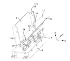
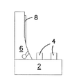
図1に図示された構造は、本明細書では印刷回路基板実装部として機能する「打抜き加工されたグリッド」(以下、単にグリッドという)2、グリッド2の頂上の縁で直交方向に配置される受容ハウジング6、及び電子部品16を具備しグリッド2と機械的及び電気的に接続するよう設計された電子印刷回路基板8を有する。グリッド2の頂上には、例えばリレー等の電気機械部品4が配置される。全体構造は、車両電気システムの一構成要素として例えば自動車に収容されるよう設計される。グリッドの頂上によって隠された、グリッド2の内側の電気機械部品4は、グリッド2の縁で互いに及び雌型(ソケット)コネクタ10のコンタクトに接続される。電子印刷回路基板8の電子部品16は、とりわけ電気機械部品4を駆動するよう作用するが、他の処理もする。電子印刷回路基板8(以下、単に印刷回路基板という)をグリッド2に機械的及び電気的に接続するために、図1では隠されておりグリッド2の(第2)コネクタ10に結合するよう設計された第1コネクタは、印刷回路基板8の下端面に配置される。
The structure shown in FIG. 1 is arranged in an orthogonal direction at the top edge of the
図1に示される構造の説明を簡単にするために、x軸、y軸、z軸を有する座標系が示される。ここで、z方向は上を示すが、構造は特定の設置位置に限定されない。グリッド2の平面はxy平面に対応し、また「水平方向」をも示す。従って、受容ハウジング6はz方向すなわち垂直方向を向く。
In order to simplify the description of the structure shown in FIG. 1, a coordinate system having an x-axis, a y-axis and a z-axis is shown. Here, although the z direction indicates the top, the structure is not limited to a specific installation position. The plane of the
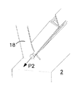
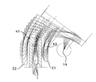
印刷回路基板8をグリッド2に接続するために、印刷回路基板8は側壁12,12'を有する。軸受ジャーナルは、図示された側壁12及び図示されていない別の側壁12の底隅に取り付けられ、旋回軸14を画定する。図1、図2及び図3から明白であるように、印刷回路基板8は、印刷回路基板8がグリッド2及び受容ハウジング6間でほぼ二等分線、すなわちx軸及びz軸間でほぼ45°を形成するように受容ハウジング6まで移動される。次に、軸受ジャーナルは2個の挿入スロット20(図1において1個の挿入スロット20のみが見える)に配置される。次に、印刷回路基板8は矢印P1(図2)及びP2(図3)の方向に並進移動される。
In order to connect the printed
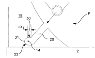
図4は、受容ハウジング6の側壁18の挿入スロット20の領域を示す。挿入スロット20は、グリッド2の頂上とほぼ平行な湾曲部に隣接する、比較的長い直線部を有する。挿入スロット20の端部は、以下に詳細に説明される軸受ジャーナル用の横方向停止面31を形成する。軸受ジャーナルは旋回軸14の中心に位置する。挿入スロット20の端部の横方向停止面31、挿入スロット20の端部の下側領域、及び上側制限停止部30を形成する上側領域は、軸受ジャーナル着座部22を形成する。受容ハウジング6の2側壁18の挿入スロット20内に軸受ジャーナルを斜めに挿入した後、軸受ジャーナルは軸受ジャーナル着座部22内に完全には配置されない。−x1(図4参照)の量だけさらに変位させた後のみ、旋回軸14は、印刷回路基板8の旋回が可能な位置に到達する。図4に従った点で印刷回路基板8が旋回軸14と共につく位置は、仮捕捉位置を示す。
FIG. 4 shows the area of the
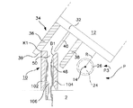
図5は、旋回軸14と直角の部分断面図を示す。ここで第2コネクタに指定されたコネクタ10が、グリッド2の頂上の縁に見える(受容ハウジング6は図5に指示されていない)。
FIG. 5 shows a partial cross-sectional view perpendicular to the
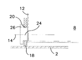
第2コネクタ10は、旋回軸14に対して外側に配置された第2外壁102、第2外壁102と共に形成する第2内壁104、雌型(ソケット)コンタクト106が収容されたコンタクト受容室48を有する。第2外壁102及び第2内壁104の上側且つ内側の端は内側に突出するので、挿入されるブレードコンタクト40を保護するために雌型コンタクトの端部を超えて突出する。第2コネクタ10と嵌合する第1コネクタ34は、印刷回路基板8の下側端面に配置される。図5では、側面12の底側端部のみが見える。第1コネクタ34は、旋回軸14に対して外側に配置された第1外壁36、第1内壁38、雄型コンタクト40を構成する上述のブレードコンタクトを有する。旋回軸14に面する第1外壁36の内側端部は面取り39を具備する。
The
図5は、印刷回路基板8を挿入スロット20内に挿入し、湾曲した矢印Pに従って印刷回路基板を仮捕捉位置に変位させた後の状態を示す。印刷回路基板8は、本工程中、上述の軸により挿入スロット20内に案内される。
FIG. 5 shows a state after the printed
図7は、側壁12が固定された印刷回路基板8の底隅を部分的に断面した図を示す。その外側底端部には軸受ジャーナル24が固定され、軸受ジャーナル24の端部は突出フランジ26により終端される。印刷回路基板8の他の底点部に対称的に配置された軸受ジャーナルと共に、図7に示されたフランジ26を有する軸受ジャーナル24は旋回軸14を画定する。フランジ26及び側壁12の外側間の距離は受容ハウジング6の側壁18の厚さより若干大きく、軸受ジャーナル24の直径は挿入スロット22の幅より若干小さい。この結果、印刷回路基板8は、仮捕捉位置に移動すると最小限の遊びを伴って案内される。
FIG. 7 is a partial cross-sectional view of the bottom corner of the printed
図5において、湾曲矢印Pの先端は仮捕捉位置に対応する。矢印の湾曲部では、すなわち仮捕捉位置に到達する前には、第1外壁36の傾斜面39の領域の底縁が第2コネクタ10の第2外壁102の上縁に接触する。これにより、仮捕捉位置に到達する前の印刷回路基板8の旋回が阻止される。しかし、図5の図示に従った仮捕捉位置に到達すると、印刷回路基板の旋回を阻止するものは何もない。矢印P3方向に従った旋回中に、第2コネクタ10の第2外壁102の左上縁は、摺動案内領域K1内で第1外壁36の内面に接触する。この状態において、図5における右(図1におけるx軸の方向)への並進移動は、第2コネクタ10の第2外壁102及び第1コネクタ34の第1外壁36の摺動接触点K1での接触により阻止される。構造の上方への移動は、挿入スロット(図4)の最終部分の上側制限停止部30に対する軸24の上側領域の載置により阻止される。
In FIG. 5, the tip of the curved arrow P corresponds to the temporary capture position. In the curved portion of the arrow, that is, before reaching the temporary capture position, the bottom edge of the region of the
図5は、第1コネクタ34を有する印刷回路基板の旋回の結果、ブレードコンタクト40が挿入開口50内に、次に雌型(ソケット)コンタクト106内に入ることを示す。
FIG. 5 shows that as a result of the swiveling of the printed circuit board having the
図6は、旋回接続工程の個々の段階を示す。図6は、旋回移動の大部分の際、コネクタ10,34の2個の外壁102,36が摺動案内領域K1で接触することを示す。旋回移動中、第2コネクタ10の第2外壁102より短い第2内壁104の円弧面領域B1(図5参照)は、ブレードコンタクト40が衝突することなく信頼性高く第2内壁を超えて移動することを可能にする。
FIG. 6 shows the individual stages of the swivel connection process. FIG. 6 shows that the two
図6によれば、第1コネクタ34の第1内壁38の内側の面取りK2は、第2コネクタ10の第2内壁104の外側と衝突するのを防止する。第1コネクタ34の第1内壁38の自由端E1は、このコネクタ34の第1外壁の自由端E2よりも短い。
According to FIG. 6, the chamfer K <b> 2 on the inner side of the first
図8は、印刷回路基板8の旋回の後、受容ハウジング6により完全に収容される最終状態を示す。
FIG. 8 shows the final state in which the printed
上述の実施形態は、異なる多くの方法に変更可能である。例えば、挿入スロット25は受容ハウジング6の側壁18の貫通スロットの形態をとる必要はなく、代わりに側壁18の内側の溝も可能である。また、受容ハウジング6は、印刷回路基板8を完全に収容するほど十分に高くなる必要はない。上述の実施形態の雄型コンタクト及び雌型コンタクトは対向する位置を占めてもよい、すなわちブレードコンタクト40はグリッド2上のコネクタに設けられてもよく、他方、雌型コンタクトは他方のコネクタに配置されてもよい。
The embodiments described above can be modified in many different ways. For example, the insertion slot 25 need not take the form of a through slot in the
コネクタ分野の当業者であれば、上述した本発明及び特許請求の範囲で定義された範囲を逸脱することなく、多数の変形可能性があることを認識すべきである。 Those skilled in the connector arts should recognize that there are numerous variations without departing from the scope defined in the present invention and the claims set forth above.
2 印刷回路基板実装部
6 受容ハウジング
8 印刷回路基板
10 第2コネクタ
12 側壁
14 旋回軸(旋回接続デバイス)
18 側壁
20 挿入スロット
24 軸受ジャーナル
30 上側制限停止部(旋回接続デバイス)
31 旋回接続デバイス
34 第1コネクタ
36 第1外壁
38 第1内壁
40 コンタクト
48 コンタクト受容室
50 挿入開口
102 第2外壁
104 第2内壁
106 第2コンタクト
K1 摺動案内領域(旋回接続デバイス)
2 Printed circuit
18
31
Claims (10)
制限的に案内された旋回接続デバイスを具備することを特徴とする差込接続構造。 In the plug-in connection structure for connecting the first connector having the first contact attached to the printed circuit board to the second connector having the second contact disposed in the printed circuit board mounting portion,
Plug-in connection structure, characterized in that it comprises a limitedly guided swivel connection device.
前記第1コネクタは、前記旋回軸に対して外側に配置された第1外壁と、該第1外壁に対して内側に配置された第1内壁と、前記第1外壁及び前記第1内壁間に配置された1列のコンタクトとを具備し、
前記第2コネクタは、コンタクトが間に配置された第2外壁及び第2内壁を具備し、
前記第2外壁及び前記第2内壁は、接続状態において、前記第1コネクタの前記第1外壁及び前記第1内壁により取り囲まれることを特徴とする請求項1記載の差込接続構造。 A swivel axis is provided on the printed circuit board,
The first connector includes a first outer wall disposed on the outer side with respect to the pivot axis, a first inner wall disposed on the inner side with respect to the first outer wall, and the first outer wall and the first inner wall. A row of arranged contacts,
The second connector includes a second outer wall and a second inner wall with contacts arranged therebetween,
The plug-in connection structure according to claim 1, wherein the second outer wall and the second inner wall are surrounded by the first outer wall and the first inner wall of the first connector in a connected state.
該両側壁から、軸受ジャーナルが外方に突出して前記旋回軸を画定し、
前記印刷回路基板実装部の頂上に、2個の側壁を有する受容ハウジングがほぼ直角に取り付けられ、
前記2個の側壁間で前記第2コネクタが前記旋回軸に平行に延びており、
前記2個の側壁には、前記軸受ジャーナル用の挿入スロットが形成されていることを特徴とする請求項1又は請求項2記載の差込接続構造。 The printed circuit board and the first connector have side walls;
From the side walls, a bearing journal projects outwardly to define the pivot axis,
A receiving housing having two side walls is mounted on the top of the printed circuit board mounting portion at a substantially right angle;
The second connector extends parallel to the pivot axis between the two side walls;
The insertion connection structure according to claim 1 or 2, wherein an insertion slot for the bearing journal is formed in the two side walls.
前記挿入スロットは、仮捕捉位置を画定する端部領域を有し、
前記仮捕捉位置から、前記印刷回路基板が再度抜去されるか、又は最終接続位置へ旋回することができることを特徴とする請求項3ないし請求項5のうちいずれか1項記載の差込接続構造。 The insertion slot determines a direction in which the printed circuit board is introduced by the bearing journal substantially parallel to a plane of the printed circuit board;
The insertion slot has an end region defining a temporary capture position;
The plug-in connection structure according to any one of claims 3 to 5, wherein the printed circuit board can be removed again from the temporary capture position or swiveled to a final connection position. .
前記第2コネクタの前記第2外壁及び前記第2内壁は、それらの自由端で、下流の前記コンタクト受容室よりも狭く前記雌型コンタクトの端面端部を超えて突出する嵌合コンタクト挿入開口を形成することを特徴とする請求項2ないし請求項8のうちいずれか1項記載の差込接続構造。 The contacts of the second connector take the form of female contacts;
The second outer wall and the second inner wall of the second connector have, at their free ends, a fitting contact insertion opening that is narrower than the downstream contact receiving chamber and protrudes beyond the end portion of the female contact. The plug-in connection structure according to any one of claims 2 to 8, wherein the plug-in connection structure is formed.
Applications Claiming Priority (1)
| Application Number | Priority Date | Filing Date | Title |
|---|---|---|---|
| DE10359232A DE10359232A1 (en) | 2003-12-17 | 2003-12-17 | PCB connector |
Publications (2)
| Publication Number | Publication Date |
|---|---|
| JP2005183380A true JP2005183380A (en) | 2005-07-07 |
| JP2005183380A5 JP2005183380A5 (en) | 2005-09-22 |
Family
ID=34485436
Family Applications (1)
| Application Number | Title | Priority Date | Filing Date |
|---|---|---|---|
| JP2004358794A Withdrawn JP2005183380A (en) | 2003-12-17 | 2004-12-10 | Plug-in connection structure |
Country Status (4)
| Country | Link |
|---|---|
| US (1) | US7101198B2 (en) |
| EP (1) | EP1544957A1 (en) |
| JP (1) | JP2005183380A (en) |
| DE (1) | DE10359232A1 (en) |
Cited By (1)
| Publication number | Priority date | Publication date | Assignee | Title |
|---|---|---|---|---|
| JP4719305B1 (en) * | 2010-08-27 | 2011-07-06 | イリソ電子工業株式会社 | connector |
Families Citing this family (5)
| Publication number | Priority date | Publication date | Assignee | Title |
|---|---|---|---|---|
| DE10359232A1 (en) | 2003-12-17 | 2005-07-21 | Tyco Electronics Amp Gmbh | PCB connector |
| US7479020B2 (en) * | 2004-11-22 | 2009-01-20 | Visteon Global Technologies, Inc. | Electronic control module having an internal electric ground |
| CN103682816A (en) * | 2013-11-25 | 2014-03-26 | 泰兴市航联电连接器有限公司 | Active guide positioning and separating electric connector |
| JP6997127B2 (en) * | 2019-03-26 | 2022-01-17 | ヒロセ電機株式会社 | Connector device and connector |
| CN112261344B (en) * | 2020-09-11 | 2022-10-25 | 安徽阿瑞斯科技有限公司 | Multifunctional conference machine with protective structure and embedded 5G module |
Family Cites Families (8)
| Publication number | Priority date | Publication date | Assignee | Title |
|---|---|---|---|---|
| SU871264A1 (en) * | 1980-01-03 | 1981-10-07 | Предприятие П/Я А-1335 | Multi-contact electrical connector |
| US4972296A (en) * | 1989-06-15 | 1990-11-20 | Northern Telecom Limited | Expandable modular switching unit |
| GB9127466D0 (en) | 1991-12-30 | 1992-02-19 | Amp Gmbh | Electronic control module assembly |
| JP2909525B2 (en) * | 1993-04-19 | 1999-06-23 | 矢崎総業株式会社 | Connector device |
| JPH11283699A (en) * | 1998-03-31 | 1999-10-15 | Yazaki Corp | Connector structure |
| FR2782577B1 (en) * | 1998-08-24 | 2000-11-17 | Framatome Connectors Int | CONNECTOR WITH PLUG AND LOW INSERTION SOCKET, IN PARTICULAR OF THE PIN / LYRE CONTACTS TYPE |
| US6676430B1 (en) * | 2000-05-23 | 2004-01-13 | Avaya Technology Corp. | Board mounted jack module |
| DE10359232A1 (en) | 2003-12-17 | 2005-07-21 | Tyco Electronics Amp Gmbh | PCB connector |
-
2003
- 2003-12-17 DE DE10359232A patent/DE10359232A1/en not_active Ceased
-
2004
- 2004-12-07 EP EP04028961A patent/EP1544957A1/en not_active Withdrawn
- 2004-12-10 JP JP2004358794A patent/JP2005183380A/en not_active Withdrawn
- 2004-12-13 US US11/010,582 patent/US7101198B2/en not_active Expired - Fee Related
Cited By (6)
| Publication number | Priority date | Publication date | Assignee | Title |
|---|---|---|---|---|
| JP4719305B1 (en) * | 2010-08-27 | 2011-07-06 | イリソ電子工業株式会社 | connector |
| WO2012026153A1 (en) * | 2010-08-27 | 2012-03-01 | イリソ電子工業株式会社 | Connector |
| JP2012049002A (en) * | 2010-08-27 | 2012-03-08 | Iriso Electronics Co Ltd | Connector |
| CN103098306A (en) * | 2010-08-27 | 2013-05-08 | 意力速电子工业株式会社 | Connector |
| CN103098306B (en) * | 2010-08-27 | 2015-07-15 | 意力速电子工业株式会社 | Connector |
| US9105997B2 (en) | 2010-08-27 | 2015-08-11 | Iriso Electronics Co., Ltd. | Connector |
Also Published As
| Publication number | Publication date |
|---|---|
| DE10359232A1 (en) | 2005-07-21 |
| US20050153579A1 (en) | 2005-07-14 |
| EP1544957A1 (en) | 2005-06-22 |
| US7101198B2 (en) | 2006-09-05 |
Similar Documents
| Publication | Publication Date | Title |
|---|---|---|
| KR100933261B1 (en) | Connector, connector assembly and its connection method | |
| US7090518B1 (en) | Electrical connector with a locking mechanism | |
| JP2006324227A (en) | Connector | |
| US7445475B2 (en) | Lever type connector | |
| US9666987B1 (en) | Connector and connector assembly | |
| JP2007173164A (en) | Connector | |
| JP2009110733A (en) | Connector | |
| US9905965B2 (en) | Connector and connector assembly | |
| EP0797274B1 (en) | Connector connecting structure | |
| JP2005183380A (en) | Plug-in connection structure | |
| US9853395B2 (en) | Connector and connector assembly | |
| KR20140031151A (en) | Connector device | |
| CN108352656B (en) | Connector device | |
| US10587076B2 (en) | Connector position assurance member | |
| US6220886B1 (en) | Connector | |
| JP2010108872A (en) | Lever-type connector | |
| JP2008226535A (en) | Lever-type connector | |
| US10505314B1 (en) | Electrical connector with a connector position assurance member for a shrouded latch | |
| EP1463157B1 (en) | Stepped keying/interface stabilization alignment mechanism | |
| US9780477B1 (en) | Box terminal with insertion limiter | |
| JP2009048890A (en) | Split connector | |
| JP6567852B2 (en) | Floating connector device | |
| US20030114038A1 (en) | Connector construction and a method for connecting a pair of connectors | |
| JP2018018615A (en) | Electric connector assembly and electric connector | |
| JP2008153055A (en) | Terminal metal fitting, connector, and connector connecting structure |
Legal Events
| Date | Code | Title | Description |
|---|---|---|---|
| A521 | Written amendment |
Free format text: JAPANESE INTERMEDIATE CODE: A523 Effective date: 20050520 |
|
| A521 | Written amendment |
Free format text: JAPANESE INTERMEDIATE CODE: A523 Effective date: 20050616 |
|
| A621 | Written request for application examination |
Free format text: JAPANESE INTERMEDIATE CODE: A621 Effective date: 20071130 |
|
| A761 | Written withdrawal of application |
Free format text: JAPANESE INTERMEDIATE CODE: A761 Effective date: 20090803 |