JP2005158366A - Discharge lamp lighting device and luminaire - Google Patents
Discharge lamp lighting device and luminaire Download PDFInfo
- Publication number
- JP2005158366A JP2005158366A JP2003392984A JP2003392984A JP2005158366A JP 2005158366 A JP2005158366 A JP 2005158366A JP 2003392984 A JP2003392984 A JP 2003392984A JP 2003392984 A JP2003392984 A JP 2003392984A JP 2005158366 A JP2005158366 A JP 2005158366A
- Authority
- JP
- Japan
- Prior art keywords
- discharge lamp
- voltage
- lamp
- lighting device
- current
- Prior art date
- Legal status (The legal status is an assumption and is not a legal conclusion. Google has not performed a legal analysis and makes no representation as to the accuracy of the status listed.)
- Granted
Links
- 230000002159 abnormal effect Effects 0.000 claims abstract description 12
- 238000001514 detection method Methods 0.000 claims abstract description 11
- 230000005856 abnormality Effects 0.000 claims description 2
- 230000020169 heat generation Effects 0.000 abstract description 4
- 239000003381 stabilizer Substances 0.000 abstract 1
- 238000010586 diagram Methods 0.000 description 12
- 238000006243 chemical reaction Methods 0.000 description 4
- IYRDVAUFQZOLSB-UHFFFAOYSA-N copper iron Chemical compound [Fe].[Cu] IYRDVAUFQZOLSB-UHFFFAOYSA-N 0.000 description 4
- 238000000034 method Methods 0.000 description 4
- 239000003990 capacitor Substances 0.000 description 3
- IJGRMHOSHXDMSA-UHFFFAOYSA-N Atomic nitrogen Chemical compound N#N IJGRMHOSHXDMSA-UHFFFAOYSA-N 0.000 description 2
- 230000000694 effects Effects 0.000 description 2
- 239000007789 gas Substances 0.000 description 2
- 239000004020 conductor Substances 0.000 description 1
- 230000006866 deterioration Effects 0.000 description 1
- 238000009499 grossing Methods 0.000 description 1
- 239000011261 inert gas Substances 0.000 description 1
- WABPQHHGFIMREM-UHFFFAOYSA-N lead(0) Chemical compound [Pb] WABPQHHGFIMREM-UHFFFAOYSA-N 0.000 description 1
- 229910001507 metal halide Inorganic materials 0.000 description 1
- 150000005309 metal halides Chemical class 0.000 description 1
- 229910052757 nitrogen Inorganic materials 0.000 description 1
- 238000009877 rendering Methods 0.000 description 1
- 238000007789 sealing Methods 0.000 description 1
- 230000006641 stabilisation Effects 0.000 description 1
- 238000011105 stabilization Methods 0.000 description 1
- 239000004575 stone Substances 0.000 description 1
- 239000000126 substance Substances 0.000 description 1
Images
Classifications
-
- Y02B20/204—
Landscapes
- Circuit Arrangements For Discharge Lamps (AREA)
Abstract
Description
本発明はHIDランプを点灯させる放電灯点灯装置に関するものである。 The present invention relates to a discharge lamp lighting device for lighting a HID lamp.
HIDランプは、高輝度、種類によっては高効率という特徴を持つことから幅広い分野で用いられている。特に高演色のメタルハライドランプは近年その特徴を生かし、屋内の店舗等のスポットライトやダウンライト等に利用されてきている。そのため灯具のデザインも重要になり、より小型な灯具が好まれている。このことから、近年においては安定器の軽量化・小型化・高機能化を目的とした多くの電子部品を用いた電子バラストなるものが主流となりつつある。この電子バラストについて以下簡単に説明する。 HID lamps are used in a wide range of fields because of their high brightness and high efficiency depending on the type. In particular, high-color-rendering metal halide lamps have recently been used for spotlights and downlights in indoor stores, taking advantage of their characteristics. Therefore, the design of the lamp is also important, and smaller lamps are preferred. Therefore, in recent years, electronic ballasts using many electronic components for the purpose of reducing the weight, size and function of ballasts are becoming mainstream. This electronic ballast will be briefly described below.
通常、HIDランプの電子バラストは、音響的共鳴現象を回避するために矩形波点灯方式を採用することが多い。矩形波点灯方式の基本的な考え方は、ランプ電流の限流については高周波領域で行うことによって限流要素の小型化を実現し、またその一方で高周波電流を音響的共鳴現象の生じない低周波にて極性を反転させ、そのうち高周波成分をフィルタ回路にて除去した低周波成分のみの低周波電流をランプに供給することにより、音響的共鳴現象を回避しつつ安定な放電灯の点灯を実現している。 In general, the electronic ballast of an HID lamp often employs a rectangular wave lighting system in order to avoid an acoustic resonance phenomenon. The basic idea of the rectangular wave lighting method is to reduce the current limiting element by limiting the current limiting of the lamp current in the high frequency range, while reducing the high frequency current to a low frequency that does not cause an acoustic resonance phenomenon. Inverting the polarity and supplying the lamp with a low-frequency current consisting only of the low-frequency component, with the high-frequency component removed by the filter circuit, enables stable lighting of the discharge lamp while avoiding acoustic resonance. ing.
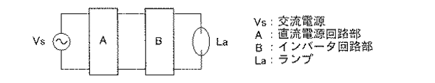
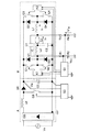
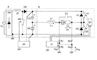
図8に電子バラストのブロック図を示す。交流電源Vsに整流回路を含む直流電源回路部Aが接続されており、この直流電源回路部Aの出力端に低周波矩形波電力を発生するインバータ回路部Bが接続されており、このインバータ回路部Bの出力端にランプLaが接続されている。なお、インバータ回路部Bはイグナイタ回路(図示せず)を具備しており、始動時には高圧パルス電圧を発生させる。 FIG. 8 shows a block diagram of the electronic ballast. A DC power supply circuit section A including a rectifier circuit is connected to the AC power supply Vs, and an inverter circuit section B that generates low-frequency rectangular wave power is connected to an output terminal of the DC power supply circuit section A. This inverter circuit The lamp La is connected to the output end of the part B. The inverter circuit unit B includes an igniter circuit (not shown), and generates a high voltage pulse voltage at the time of starting.
図8のブロック図のさらに具体的な回路図を図9に示す。直流電源回路部Aは整流回路DBとスイッチング素子Q0とダイオードD0とインダクタンスL0とコンデンサC0と制御回路S0からなり、スイッチング素子Q0、ダイオードD0、インダクタンスL0により昇圧チョッパ回路を構成し、交流電源Vsの交流電圧を直流電圧に整流・平滑する機能を有する。昇圧チョッパ回路の動作については、一般的であるため省略する。 A more specific circuit diagram of the block diagram of FIG. 8 is shown in FIG. The DC power supply circuit section A includes a rectifier circuit DB, a switching element Q0, a diode D0, an inductance L0, a capacitor C0, and a control circuit S0. The switching element Q0, the diode D0, and the inductance L0 constitute a boost chopper circuit, and the AC power supply Vs It has the function of rectifying and smoothing AC voltage into DC voltage. Since the operation of the step-up chopper circuit is general, it will be omitted.
また、インバータ回路部Bはスイッチング素子Q1〜Q4とダイオードD1〜D4とインダクタンスL1とコンデンサC1と制御回路S1とドライバIC(例えばIR社製IR2308)K1、K2とからなる。制御回路S1はランプLaのランプ電圧を抵抗R1〜R4によって検出し、ランプ電圧に応じてスイッチング素子Q1〜Q4のON/OFF制御を行ない、ランプLaに適当な電力を供給する。 The inverter circuit section B includes switching elements Q1 to Q4, diodes D1 to D4, an inductance L1, a capacitor C1, a control circuit S1, and driver ICs (for example, IR2308 manufactured by IR) K1 and K2. The control circuit S1 detects the lamp voltage of the lamp La with resistors R1 to R4, performs ON / OFF control of the switching elements Q1 to Q4 according to the lamp voltage, and supplies appropriate power to the lamp La.
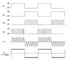
図10に各スイッチング素子Q1〜Q4のタイミングチャートを示す。点灯時において、スイッチング素子Q1、Q2は数10〜数100Hzで動作し、スイッチング素子Q3、Q4は数10KHzで動作することによって、インダクタンスL1には図10のIL1のような電流が流れる。また、ランプLaにはコンデンサC1によってIL1の高周波成分を除去したIlaのような略矩形波電流が流れる。 FIG. 10 shows a timing chart of the switching elements Q1 to Q4. At the time of lighting, the switching elements Q1 and Q2 operate at several tens to several hundreds Hz, and the switching elements Q3 and Q4 operate at several tens KHz, so that a current like I L1 in FIG. 10 flows through the inductance L1. Further, a substantially rectangular wave current such as Ila from which the high frequency component of I L1 has been removed by the capacitor C1 flows through the lamp La.
ここで、制御回路S1はマイコンを用いてもよい。その場合、ランプ電圧は抵抗R1〜R4により分圧された電圧をマイコンによりA/D変換した値をランプ電圧値として認識する。すなわち、ランプ電圧を検出するには、抵抗R2の両端電圧VR2と抵抗R4の両端電圧VR4の差の絶対値を求めることで、ランプ電圧値として認識することができる。 Here, the control circuit S1 may use a microcomputer. In that case, the lamp voltage recognizes the value obtained by A / D converting the voltage divided by the resistors R1 to R4 as a lamp voltage value. That is, in order to detect the lamp voltage, the absolute value of the difference between the both-ends voltage V R2 of the resistor R2 and the both-ends voltage V R4 of the resistor R4 can be obtained and recognized as the lamp voltage value.
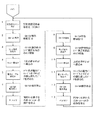
図11にマイコンのメインプログラムのフローチャートを示す。以下、簡単にプログラムの動作を説明する。まず、矩形波の低周波数を設定する。ここでは170Hzとした。その後、スイッチング素子Q2、Q3が図10に示したように動作をする。そして、矩形波周波数の半サイクルの間のランプ電圧を読み込み、A/D変換し、Vla2として値を書き込む。その値から予めマイコンの中に収めておいたランプ電圧−ランプ電力データテーブルより適した電力を読み込む。その後、スイッチング素子Q2、Q3は動作を停止し、スイッチング素子Q1〜Q4が同時オンしないように、全スイッチング素子をオフしている(ステップ1〜7)。
FIG. 11 shows a flowchart of the main program of the microcomputer. The operation of the program will be briefly described below. First, the low frequency of a rectangular wave is set. Here, it was set to 170 Hz. Thereafter, the switching elements Q2 and Q3 operate as shown in FIG. Then, the lamp voltage during a half cycle of the rectangular wave frequency is read, A / D converted, and a value is written as Vla2. From the value, a suitable power is read from the lamp voltage-lamp power data table stored in the microcomputer in advance. Thereafter, the switching elements Q2 and Q3 stop operating, and all the switching elements are turned off so that the switching elements Q1 to Q4 are not turned on simultaneously (
次に、スイッチング素子Q1、Q4は1回前のランプ電圧に応じた電力テーブルに則った電力をランプに供給できるようにON/OFF動作する。そして、低周波の半サイクル間のランプ電圧のA/D変換値をVla1として値を書き込み、電力テーブルを読み込む。その後、スイッチング素子Q1、Q4が動作を停止した後、先ほどと同じく全スイッチング素子をオフしたのち、再度スイッチング素子Q2、Q3の動作に戻り、以上の動作を繰り返すことでランプに適当な電力供給を行うことかできる(ステップ8〜13)。 Next, the switching elements Q1 and Q4 perform an ON / OFF operation so that power can be supplied to the lamp in accordance with the power table corresponding to the lamp voltage one time before. Then, the A / D conversion value of the lamp voltage during the low frequency half cycle is written as Vla1, and the power table is read. Thereafter, after the switching elements Q1 and Q4 stop operating, all the switching elements are turned off as before, and then the operation returns to the operation of the switching elements Q2 and Q3 again. Can be performed (steps 8-13).
一般的に高圧放電灯は点灯初期から点灯時間が経過していくにしたがってランプ電圧が上昇していく傾向にある。通常、銅鉄式安定器であれば、このようにランプ電圧が上昇していくと、ランプの再点弧電圧が上昇するため点灯維持できなくなり、立ち消えを起こしていた。 In general, a high-pressure discharge lamp tends to increase the lamp voltage as the lighting time elapses from the beginning of lighting. Normally, in the case of a copper-iron type ballast, when the lamp voltage increases in this way, the re-ignition voltage of the lamp increases, so that the lighting cannot be maintained and the lamp is extinguished.
一方、電子バラストでは寿命末期においても再点弧電圧が銅鉄安定器に比べて出にくくなるため、なかなか立ち消えにはならない。その点でランプの寿命を延ばすことにもなっていた。しかし、立ち消えを起こさないので、ランプには銅鉄式安定器に比べてさらに負荷をかけることになるため、ランプ内部の発光管が劣化し、クラック等を起こす場合がある。その際、ランプの発光効率を向上させるためにランプ外管内を真空にした高圧放電灯においては、発光管から外管内に発光物質等が放出される場合がある。この場合、真空であった外管内が真空でなくなり、ガスの圧力が上昇するので、外管内の電位差がある導体間で放電が起こることがある。本明細書中、このような発光管の異常により外管内で生じる放電を「外管内放電」と称する。この外管内放電が生じると、定格電流値を超える過電流が安定器から供給されることにより、安定器の温度上昇が大きくなり、ランプの口金部およびランプソケットやリード線においても通常より発熱して寿命劣化を招く。この外管内放電は銅鉄安定器においても同様に起こることがある。 On the other hand, in the electronic ballast, the re-ignition voltage is less likely to occur at the end of the life than the copper iron ballast, so it does not disappear easily. In this respect, the lamp life was also extended. However, since the lamp does not go out, the lamp is further loaded as compared with the copper-iron ballast, so that the arc tube inside the lamp may be deteriorated and cracks may occur. At that time, in a high-pressure discharge lamp in which the inside of the lamp outer tube is evacuated in order to improve the luminous efficiency of the lamp, a luminescent substance or the like may be emitted from the arc tube into the outer tube. In this case, the inside of the outer tube that has been evacuated is no longer vacuum, and the gas pressure rises, so that discharge may occur between conductors having a potential difference in the outer tube. In the present specification, the discharge generated in the outer tube due to the abnormality of the arc tube is referred to as “outer tube discharge”. If this discharge occurs in the outer tube, the overcurrent exceeding the rated current value is supplied from the ballast, which increases the temperature of the ballast, and heat is generated more than usual in the lamp cap, lamp socket, and lead wire. This will lead to life deterioration. This outer tube discharge may occur in a copper-iron ballast as well.
この外管内放電を未然に防止する手段としては外管内に窒素などの不活性ガスを封入する方法が知られているが、この場合においては外管内のガスにより発光管の熱が外部へ伝わりやすくなり、発光管温度が低下してしまうために、効率が低下してしまう。 As a means for preventing the discharge in the outer tube, a method of sealing an inert gas such as nitrogen in the outer tube is known. In this case, the heat in the arc tube is easily transmitted to the outside by the gas in the outer tube. As a result, the arc tube temperature is lowered, and the efficiency is lowered.
また、外管内放電が起こり過電流が流れた時にこれを遮断する手段として、電流ヒューズを口金内に配設し、過電流により電流ヒューズを溶断させ、供給電力を切断する方法も知られている(特許第3126300号)。この場合においては、ランプの始動時には安定時よりも大きい電流が流れるため、その電流値で溶断しない電流ヒューズを用いる必要がある。そのため外管内放電が生じて過電流が流れてもその電流値によっては電流ヒューズが溶断されるまでに長時間を要したり、溶断まで至らない場合がある。したがって、この電流ヒューズによっては、安定器やソケット等の損傷を確実に防ぐことはできない。また、口金部が高温になるために電流ヒューズが酸化して不導体になり、ランプが不点灯になる恐れもある。
本発明は、以上のような点を解決すべく考案されたものであり、その目的とするところは、外管内放電状態のランプが負荷となっても安定器やランプソケットの異常発熱を防止できる放電灯点灯装置を提供することにある。 The present invention has been devised to solve the above-mentioned points, and the object of the present invention is to prevent abnormal heat generation of the ballast and the lamp socket even when the lamp in the discharge state in the outer tube becomes a load. The object is to provide a discharge lamp lighting device.
本発明にあっては、上記の課題を解決するために、少なくともスイッチング素子を含む点灯回路により低周波の略矩形波電力を高圧放電灯に与えて点灯させる放電灯点灯装置において、放電灯の電圧又は電流の瞬時値を検出する検出手段を備え、前記検出手段により略矩形波の極牲反転直後又は極性反転からある一定期間の電圧又は電流の瞬時値レベルを検出し、所定の閾値を超えた場合には異常と判定して、点灯回路の出力を停止又は低減することを特徴とするものである。つまり、矩形波反転直後の瞬時電圧(再点弧電圧)あるいは瞬時電流(オーバーシュート電流)を読み込み、所定の閾値と比較することで、外管内放電状態のランプと正常ランプを区別する。 In the present invention, in order to solve the above-described problems, in a discharge lamp lighting device for lighting a high-pressure discharge lamp by applying a low-frequency substantially rectangular wave power by a lighting circuit including at least a switching element, the voltage of the discharge lamp Or a detecting means for detecting an instantaneous value of the current, and the detecting means detects an instantaneous value level of the voltage or current for a certain period immediately after the polarity inversion of the substantially rectangular wave or from the polarity inversion, and exceeds a predetermined threshold value. In this case, it is determined that the output is abnormal, and the output of the lighting circuit is stopped or reduced. In other words, the instantaneous voltage (re-ignition voltage) or instantaneous current (overshoot current) immediately after the reversal of the rectangular wave is read and compared with a predetermined threshold value, so that the lamp in the outer tube discharge state is distinguished from the normal lamp.
本発明によれば、極性反転直後のランプ電圧もしくはランプ電流の瞬時値と所定の閾値を比較することにより、外管内放電の状態にあるランプを判別し、点灯装置の出力を停止又は低減することで、外管内放電の状態となったランプにおける異常発熱を抑制することができるという効果がある。 According to the present invention, the lamp voltage or lamp current immediately after polarity inversion is compared with a predetermined threshold value to determine a lamp in a state of discharge in the outer tube, and the output of the lighting device is stopped or reduced. Thus, there is an effect that it is possible to suppress abnormal heat generation in the lamp that is in the state of discharge in the outer tube.
本発明の好ましい実施形態においては、ランプの外管内放電状態を上述した極性反転後の瞬時電圧に着目して検出するものである。本実施形態の回路図は図9とし、その制御回路S1のメイン動作のフローは図11とする。 In a preferred embodiment of the present invention, the discharge state in the outer bulb of the lamp is detected by paying attention to the instantaneous voltage after the polarity inversion described above. The circuit diagram of this embodiment is shown in FIG. 9, and the flow of the main operation of the control circuit S1 is shown in FIG.
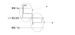
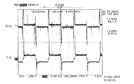
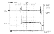
ランプが何らかの理由で発光管が破損し、外管内放電状態になると、図12に示すようなランプ電圧及びランプ電圧波形として観測される。図12の波形は、フィリップス社製CDM−T150Wランプの外管内放電状態のときのランプ電圧Vla、ランプ電流Ilaの波形である。図12から分かるように、ランプが外管内放電状態になると、ランプ電圧波形の極性反転直後に急峻な電圧波形(瞬時電圧)として観測される。また、ランプ電流に関しては、極性反転直後からランプ電圧の瞬時電圧が無くなった瞬間に急峻な電流波形(オーバーシュート電流)として観測される。 When the arc tube breaks for some reason and the discharge state is in the outer tube, the lamp voltage and the lamp voltage waveform as shown in FIG. 12 are observed. The waveforms in FIG. 12 are the waveforms of the lamp voltage Vla and the lamp current Ila when the Philips CDM-T150W lamp is in the discharge state in the outer tube. As can be seen from FIG. 12, when the lamp is in the discharge state in the outer tube, it is observed as a steep voltage waveform (instantaneous voltage) immediately after the polarity inversion of the lamp voltage waveform. The lamp current is observed as a steep current waveform (overshoot current) at the moment when the instantaneous voltage of the lamp voltage disappears immediately after polarity reversal.
図13は図12の極性反転直後の波形の拡大図である。この波形から分かるように、ランプ電圧Vlaの瞬時電圧は極性反転直後から約200μsecの間現れ、その後、ランプ電流Ilaのオーバーシュート電流が短期間流れている。 FIG. 13 is an enlarged view of the waveform immediately after polarity inversion in FIG. As can be seen from this waveform, the instantaneous voltage of the lamp voltage Vla appears for about 200 μsec immediately after the polarity inversion, and then the overshoot current of the lamp current Ila flows for a short period.
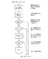
そこで、上述した極性反転後の瞬時電圧に着目してランプの外管内放電状態を検出する。その動作を図2のフローチャートと図1により説明する。図2のフローチャートは図11のフローチャートのステップ2とステップ3の間と、ステップ8とステップ9の間に挿入すればよい。まず、極性反転直後から矩形波の半サイクルの期間よりも十分に短く且つ瞬時電圧が含まれる期間t1(例えば矩形波の周波数を170Hzとした場合、500μsec程度でよい)のランプ電圧を読み込み、マイコンによりA/D変換する(ランプ瞬時電圧の読み込み)。その値をVt1とする。次に予め設定しておいた閾値VpとVt1を比較して、図1のaに示すように、Vt1の方が閾値Vpよりも大きければカウンタMに1を加える。また、図1のbに示すように、Vt1の方が閾値Vpよりも小さければ図11のフローチャートのステップ3(もしくはステップ9)へ流れる。この動作を繰り返し、カウンタMが所定回数X(例えば10回)になると、スイッチング素子Q1〜Q4の動作を停止させることで、ランプへの電力供給を停止する。
Therefore, the discharge state in the outer bulb of the lamp is detected by paying attention to the instantaneous voltage after the polarity inversion described above. The operation will be described with reference to the flowchart of FIG. 2 and FIG. The flowchart of FIG. 2 may be inserted between
すなわち、極性反転後のランプ電圧の瞬時値が閾値(定格ランプ電圧の1.5〜2倍以上に設定)を超えた回数をカウントし、所定回数になればランプ異常(外管内放電)と認識し、点灯装置の動作を停止するものである。 That is, the number of times the instantaneous value of the lamp voltage after polarity inversion exceeds a threshold value (set to 1.5 to 2 times the rated lamp voltage) is counted, and if it reaches the predetermined number, it is recognized that the lamp is abnormal (discharge in the outer tube). Then, the operation of the lighting device is stopped.
以上の動作により外管内放電の状態になったランプを検出し、点灯装置の動作を停止させることによって、点灯装置およびランプソケット、配線の異常発熱を抑えることが可能となる。 By detecting the lamp in the discharge state in the outer tube by the above operation and stopping the operation of the lighting device, it is possible to suppress abnormal heat generation of the lighting device, the lamp socket, and the wiring.
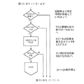
本実施例では図11に示したメインフローチャートのステップ2とステップ3、ステップ8とステップ9の間に図3のフローを挿入し、図11のステップ4とステップ5、ステップ10とステップ11の間に図4のフローを追加したものである。以下、追加したフローチャートの動作について説明する。
In this embodiment, the flow of FIG. 3 is inserted between
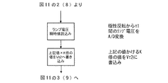
まず、極性反転直後から矩形波の半サイクルの期間よりも十分に短く且つ瞬時電圧が含まれる期間t1(例えば矩形波の周波数を170Hzとした場合、500μsec程度でよい)のランプ電圧を読み込み、マイコンによりA/D変換する(ランプ電圧瞬時値の読み込み)。その値をK倍(1.5〜2倍程度以上)した値をVt2とする(図3のフローチャート)。 First, the lamp voltage is read for a period t1 that is sufficiently shorter than the half-cycle period of the rectangular wave immediately after the polarity reversal and includes the instantaneous voltage (for example, when the frequency of the rectangular wave is 170 Hz, it may be about 500 μsec). To perform A / D conversion (reading the instantaneous value of the lamp voltage). A value obtained by multiplying the value by K (about 1.5 to 2 times or more) is defined as Vt2 (flow chart in FIG. 3).
次に、図11のメインフローチャートで得られたVla1又はVla2(矩形波半サイクルのランプ電圧のA/D変換値)とVt2(極性反転後のランプ電圧瞬時値のK倍)を比較し、Vt2の方が大きければカウンタMのカウントを1回増やす。Vt2の方が小さければ図11のフローチャートのステップ5(もしくはステップ11)へ流れる。その後、フローチャートに沿って動作を繰り返す。そしてカウンタMが所定回数X(例えば10回)になると、スイッチング素子Q1〜Q4の動作を停止させることで、ランプへの電力供給を停止する(図4のフローチャート)。 Next, Vla1 or Vla2 (A / D conversion value of the ramp voltage of the rectangular wave half cycle) and Vt2 (K times the lamp voltage instantaneous value after polarity inversion) obtained in the main flowchart of FIG. 11 are compared, and Vt2 If is greater, the counter M is incremented once. If Vt2 is smaller, the flow proceeds to step 5 (or step 11) in the flowchart of FIG. Thereafter, the operation is repeated according to the flowchart. When the counter M reaches a predetermined number of times X (for example, 10 times), the operation of the switching elements Q1 to Q4 is stopped to stop the power supply to the lamp (flowchart in FIG. 4).
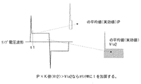
すなわち、図5に示すように、極性反転後からt1時間のランプ電圧の平均値(あるいは実効値)をPとし、これを所定倍した値(Vt2=P×K)と、半サイクルにわたるランプ電圧の平均値(あるいは実効値)であるVla2を比較して前者の方が大きい時には異常と判別し、その回数をカウントする。その回数がX回になれば点灯装置の出力を停止するものである。 That is, as shown in FIG. 5, the average value (or effective value) of the lamp voltage for t1 hours after polarity reversal is P, and a value obtained by multiplying this by a predetermined value (Vt2 = P × K) and the lamp voltage over a half cycle. The average value (or effective value) of Vla2 is compared, and when the former is larger, it is determined as abnormal, and the number of times is counted. When the number of times reaches X, the output of the lighting device is stopped.
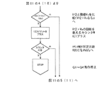
本実施例では、上述の図2のフローチャート又は図4のフローチャートの各々に「マスクカウンタ経過?」というフローを追加したものであり、それぞれ図6及び図7を用いて説明する。図中の「マスクカウンタ経過?」という比較命令は、ランプが始動してから所定時間が経過したかどうかを判定する。すなわち所定時間が経過していなければカウンタMに加算されることはない。HIDランプは正常ランプの始動直後においても極性反転直後に急峻なランプ電流波形(もしくは電圧波形)が観測されることがある。そのモードを外管内放電ランプとして誤検出しないように、ランプ始動直後からランプが安定するまでの時間(5分程度)は、カウンタMを増加させないことで正常ランプの誤検出を防ぐ効果がある。 In the present embodiment, a flow of “mask counter elapsed?” Is added to each of the flowchart of FIG. 2 or the flowchart of FIG. 4 and will be described with reference to FIGS. 6 and 7 respectively. The comparison command “mask counter elapsed?” In the figure determines whether a predetermined time has elapsed since the lamp was started. That is, if the predetermined time has not elapsed, the counter M is not added. In the HID lamp, a steep lamp current waveform (or voltage waveform) may be observed immediately after polarity inversion even immediately after starting a normal lamp. In order to prevent the mode from being erroneously detected as a discharge lamp in the outer tube, the time from the start of the lamp to the stabilization of the lamp (about 5 minutes) is effective in preventing erroneous detection of a normal lamp by not increasing the counter M.
以上のいずれの構成においても、ランプ外管内放電時におけるランプ電圧波形の極性反転直後に観測される急峻な電圧波形(瞬時電圧)を捕らえて外管内放電と判別したが、ランプ電流波形に着目してオーバーシュート電流波形を捕らえて外管内放電と判別し、点灯装置の出力を停止するプログラムとしても同様の効果が得られる。また、点灯装置の出力を低減するように制御しても良い。 In any of the above configurations, the steep voltage waveform (instantaneous voltage) observed immediately after polarity reversal of the lamp voltage waveform during the discharge in the lamp outer tube was captured and determined as the discharge in the outer tube, but attention was paid to the lamp current waveform. The same effect can be obtained as a program that captures the overshoot current waveform, determines that the discharge is in the outer tube, and stops the output of the lighting device. Moreover, you may control so that the output of a lighting device may be reduced.
なお、点灯回路については、図9のフルブリッジ形のインバータ回路を例示したが、ランプに低周波の矩形波状の電流を供給する回路方式であれば、例えば図14の降圧チョッパ回路と低周波極性反転回路を組み合わせた、いわゆる5石式でも良いし、図15のハーフブリッジ形でもよい。図中、S0,S2はチョッパ回路の制御回路、IGはイグナイタである。 As the lighting circuit, the full bridge type inverter circuit of FIG. 9 is illustrated, but if the circuit system supplies a low-frequency rectangular wave current to the lamp, for example, the step-down chopper circuit of FIG. A so-called five-stone type in which an inverting circuit is combined may be used, or the half-bridge type in FIG. In the figure, S0 and S2 are chopper circuit control circuits, and IG is an igniter.
本発明はオフィスや店舗、一般家庭用の照明器具に利用できる。 The present invention can be used in lighting equipment for offices, stores, and general homes.
Vp 外管内放電判定用の閾値
Vt1 極性反転直後のランプ電圧
Vp Threshold for determining discharge in the outer tube Vt1 Lamp voltage immediately after polarity inversion
Claims (6)
Priority Applications (5)
| Application Number | Priority Date | Filing Date | Title |
|---|---|---|---|
| JP2003392984A JP4401151B2 (en) | 2003-11-21 | 2003-11-21 | Discharge lamp lighting device and lighting fixture |
| PCT/JP2004/005823 WO2005051052A1 (en) | 2003-11-21 | 2004-04-22 | Discharge lamp ballast with detection of abnormal discharge outside the arc tube |
| CN200480034180XA CN1883238B (en) | 2003-11-21 | 2004-04-22 | Discharge lamp ballast for detecting abnormal discharge outside arc tube |
| EP04728965A EP1685749B1 (en) | 2003-11-21 | 2004-04-22 | Discharge lamp ballast with detection of abnormal discharge outside the arc tube |
| US10/578,838 US7482762B2 (en) | 2003-11-21 | 2004-04-22 | Discharge lamp ballast with detection of abnormal discharge outside the arc tube |
Applications Claiming Priority (1)
| Application Number | Priority Date | Filing Date | Title |
|---|---|---|---|
| JP2003392984A JP4401151B2 (en) | 2003-11-21 | 2003-11-21 | Discharge lamp lighting device and lighting fixture |
Publications (2)
| Publication Number | Publication Date |
|---|---|
| JP2005158366A true JP2005158366A (en) | 2005-06-16 |
| JP4401151B2 JP4401151B2 (en) | 2010-01-20 |
Family
ID=34719520
Family Applications (1)
| Application Number | Title | Priority Date | Filing Date |
|---|---|---|---|
| JP2003392984A Expired - Fee Related JP4401151B2 (en) | 2003-11-21 | 2003-11-21 | Discharge lamp lighting device and lighting fixture |
Country Status (1)
| Country | Link |
|---|---|
| JP (1) | JP4401151B2 (en) |
Cited By (3)
| Publication number | Priority date | Publication date | Assignee | Title |
|---|---|---|---|---|
| JP2008539542A (en) * | 2005-04-28 | 2008-11-13 | コーニンクレッカ フィリップス エレクトロニクス エヌ ヴィ | Projection system and method of operating a projection system |
| US8299727B1 (en) | 2009-05-12 | 2012-10-30 | Universal Lighting Technologies, Inc. | Anti-arcing protection circuit for an electronic ballast |
| US8588715B2 (en) | 2010-02-19 | 2013-11-19 | Toyota Jidosha Kabushiki Kaisha | Receiver, wireless communication system, and receiving method |
-
2003
- 2003-11-21 JP JP2003392984A patent/JP4401151B2/en not_active Expired - Fee Related
Cited By (3)
| Publication number | Priority date | Publication date | Assignee | Title |
|---|---|---|---|---|
| JP2008539542A (en) * | 2005-04-28 | 2008-11-13 | コーニンクレッカ フィリップス エレクトロニクス エヌ ヴィ | Projection system and method of operating a projection system |
| US8299727B1 (en) | 2009-05-12 | 2012-10-30 | Universal Lighting Technologies, Inc. | Anti-arcing protection circuit for an electronic ballast |
| US8588715B2 (en) | 2010-02-19 | 2013-11-19 | Toyota Jidosha Kabushiki Kaisha | Receiver, wireless communication system, and receiving method |
Also Published As
| Publication number | Publication date |
|---|---|
| JP4401151B2 (en) | 2010-01-20 |
Similar Documents
| Publication | Publication Date | Title |
|---|---|---|
| US8395327B2 (en) | High-pressure discharge lamp lighting device and lighting fixture using the same | |
| CN1846464B (en) | System and method for reducing flicker in compact gas discharge lamps at low light output levels | |
| US7042161B1 (en) | Ballast with arc protection circuit | |
| JP3315008B2 (en) | Discharge lamp lighting device | |
| CN1895006B (en) | Device for lighting high-pressure discharge lamps and lighting fixtures with the device | |
| CN101938880B (en) | ballast with end-of-life protection for one or more lamps | |
| EP1239708A2 (en) | High-intensity discharge lamp lighting apparatus and luminaire for using the same | |
| JP4598765B2 (en) | Lighting system | |
| US20100156312A1 (en) | Electronic ballast for restarting high-pressure discharge lamps in various states of operation | |
| WO2009145050A1 (en) | High-voltage discharge lamp lighting device and lighting fixture | |
| JP4401151B2 (en) | Discharge lamp lighting device and lighting fixture | |
| JP4389556B2 (en) | Discharge lamp lighting device and lighting fixture | |
| US7982411B2 (en) | Ignition and operation of electronic high intensity discharge lamps | |
| JP4239808B2 (en) | High pressure discharge lamp lighting device and lighting fixture | |
| CN1218612C (en) | Circuit arrangement | |
| CN110677951B (en) | A full-bridge resonant circuit and control method for ultrahigh-pressure mercury lamps | |
| JP2005135641A (en) | Electrodeless discharge lamp lighting device | |
| CN103379720B (en) | Lighting apparatus for discharge lamp and comprise headlamp and the vehicle of this device | |
| JP4098563B2 (en) | Power supply | |
| JP2003133098A (en) | Discharge lamp lighting device | |
| da Costa et al. | Warm-Up and Steady-State Control of High-Pressure Sodium Lamps Applied to Public Lighting Systems | |
| JPH0576158B2 (en) | ||
| AU2008100056A4 (en) | An electronic ballast igniter circuit | |
| JP2010044980A (en) | Lighting device for discharge lamp, and illumination apparatus | |
| CN107318209A (en) | A kind of high-low pressure firing circuit for metal halogen lamp electric ballast |
Legal Events
| Date | Code | Title | Description |
|---|---|---|---|
| A621 | Written request for application examination |
Free format text: JAPANESE INTERMEDIATE CODE: A621 Effective date: 20061011 |
|
| A131 | Notification of reasons for refusal |
Free format text: JAPANESE INTERMEDIATE CODE: A131 Effective date: 20080722 |
|
| A521 | Written amendment |
Free format text: JAPANESE INTERMEDIATE CODE: A523 Effective date: 20080918 |
|
| A02 | Decision of refusal |
Free format text: JAPANESE INTERMEDIATE CODE: A02 Effective date: 20081021 |
|
| A521 | Written amendment |
Free format text: JAPANESE INTERMEDIATE CODE: A523 Effective date: 20081218 |
|
| A01 | Written decision to grant a patent or to grant a registration (utility model) |
Free format text: JAPANESE INTERMEDIATE CODE: A01 |
|
| A61 | First payment of annual fees (during grant procedure) |
Free format text: JAPANESE INTERMEDIATE CODE: A61 Effective date: 20091027 |
|
| R150 | Certificate of patent (=grant) or registration of utility model |
Free format text: JAPANESE INTERMEDIATE CODE: R150 |
|
| FPAY | Renewal fee payment (prs date is renewal date of database) |
Free format text: PAYMENT UNTIL: 20121106 Year of fee payment: 3 |
|
| FPAY | Renewal fee payment (prs date is renewal date of database) |
Free format text: PAYMENT UNTIL: 20121106 Year of fee payment: 3 |
|
| FPAY | Renewal fee payment (prs date is renewal date of database) |
Free format text: PAYMENT UNTIL: 20131106 Year of fee payment: 4 |
|
| LAPS | Cancellation because of no payment of annual fees |