JP2005101537A - Lithography and method of manufacturing device using same - Google Patents
Lithography and method of manufacturing device using same Download PDFInfo
- Publication number
- JP2005101537A JP2005101537A JP2004211693A JP2004211693A JP2005101537A JP 2005101537 A JP2005101537 A JP 2005101537A JP 2004211693 A JP2004211693 A JP 2004211693A JP 2004211693 A JP2004211693 A JP 2004211693A JP 2005101537 A JP2005101537 A JP 2005101537A
- Authority
- JP
- Japan
- Prior art keywords
- exposure apparatus
- gas
- wafer
- reticle
- space
- Prior art date
- Legal status (The legal status is an assumption and is not a legal conclusion. Google has not performed a legal analysis and makes no representation as to the accuracy of the status listed.)
- Withdrawn
Links
Images


Classifications
-
- G—PHYSICS
- G03—PHOTOGRAPHY; CINEMATOGRAPHY; ANALOGOUS TECHNIQUES USING WAVES OTHER THAN OPTICAL WAVES; ELECTROGRAPHY; HOLOGRAPHY
- G03F—PHOTOMECHANICAL PRODUCTION OF TEXTURED OR PATTERNED SURFACES, e.g. FOR PRINTING, FOR PROCESSING OF SEMICONDUCTOR DEVICES; MATERIALS THEREFOR; ORIGINALS THEREFOR; APPARATUS SPECIALLY ADAPTED THEREFOR
- G03F7/00—Photomechanical, e.g. photolithographic, production of textured or patterned surfaces, e.g. printing surfaces; Materials therefor, e.g. comprising photoresists; Apparatus specially adapted therefor
- G03F7/70—Microphotolithographic exposure; Apparatus therefor
- G03F7/708—Construction of apparatus, e.g. environment aspects, hygiene aspects or materials
- G03F7/70908—Hygiene, e.g. preventing apparatus pollution, mitigating effect of pollution or removing pollutants from apparatus
- G03F7/70933—Purge, e.g. exchanging fluid or gas to remove pollutants
-
- G—PHYSICS
- G03—PHOTOGRAPHY; CINEMATOGRAPHY; ANALOGOUS TECHNIQUES USING WAVES OTHER THAN OPTICAL WAVES; ELECTROGRAPHY; HOLOGRAPHY
- G03F—PHOTOMECHANICAL PRODUCTION OF TEXTURED OR PATTERNED SURFACES, e.g. FOR PRINTING, FOR PROCESSING OF SEMICONDUCTOR DEVICES; MATERIALS THEREFOR; ORIGINALS THEREFOR; APPARATUS SPECIALLY ADAPTED THEREFOR
- G03F7/00—Photomechanical, e.g. photolithographic, production of textured or patterned surfaces, e.g. printing surfaces; Materials therefor, e.g. comprising photoresists; Apparatus specially adapted therefor
- G03F7/70—Microphotolithographic exposure; Apparatus therefor
- G03F7/708—Construction of apparatus, e.g. environment aspects, hygiene aspects or materials
- G03F7/70858—Environment aspects, e.g. pressure of beam-path gas, temperature
- G03F7/70883—Environment aspects, e.g. pressure of beam-path gas, temperature of optical system
- G03F7/70891—Temperature
-
- G—PHYSICS
- G03—PHOTOGRAPHY; CINEMATOGRAPHY; ANALOGOUS TECHNIQUES USING WAVES OTHER THAN OPTICAL WAVES; ELECTROGRAPHY; HOLOGRAPHY
- G03F—PHOTOMECHANICAL PRODUCTION OF TEXTURED OR PATTERNED SURFACES, e.g. FOR PRINTING, FOR PROCESSING OF SEMICONDUCTOR DEVICES; MATERIALS THEREFOR; ORIGINALS THEREFOR; APPARATUS SPECIALLY ADAPTED THEREFOR
- G03F7/00—Photomechanical, e.g. photolithographic, production of textured or patterned surfaces, e.g. printing surfaces; Materials therefor, e.g. comprising photoresists; Apparatus specially adapted therefor
- G03F7/70—Microphotolithographic exposure; Apparatus therefor
- G03F7/708—Construction of apparatus, e.g. environment aspects, hygiene aspects or materials
- G03F7/70908—Hygiene, e.g. preventing apparatus pollution, mitigating effect of pollution or removing pollutants from apparatus
- G03F7/70916—Pollution mitigation, i.e. mitigating effect of contamination or debris, e.g. foil traps
Landscapes
- Health & Medical Sciences (AREA)
- Epidemiology (AREA)
- Public Health (AREA)
- Life Sciences & Earth Sciences (AREA)
- Atmospheric Sciences (AREA)
- Engineering & Computer Science (AREA)
- Environmental & Geological Engineering (AREA)
- Physics & Mathematics (AREA)
- General Physics & Mathematics (AREA)
- Toxicology (AREA)
- Exposure Of Semiconductors, Excluding Electron Or Ion Beam Exposure (AREA)
- Exposure And Positioning Against Photoresist Photosensitive Materials (AREA)
Abstract
Description
本発明は微細な回路パターンを転写するための露光装置に関するものである。 The present invention relates to an exposure apparatus for transferring a fine circuit pattern.
従来、半導体メモリや論理回路などの微細な半導体素子を製造するための焼き付け(リソグラフィー)方法として、紫外線を用いた縮小投影露光が行われてきた。 Conventionally, reduction projection exposure using ultraviolet rays has been performed as a printing (lithography) method for manufacturing fine semiconductor elements such as semiconductor memories and logic circuits.
縮小投影露光で転写できる最小の寸法は転写に用いる光の波長に比例し、投影光学系の開口数に反比例する。このため微細な回路パターンを転写するために露光光の短波長化が進められ、水銀ランプi線(波長365nm)、KrFエキシマレーザー(波長248nm)、ArFエキシマレーザー(波長193nm)と用いられる紫外光の波長は短くなってきた。 The minimum dimension that can be transferred by reduction projection exposure is proportional to the wavelength of light used for transfer and inversely proportional to the numerical aperture of the projection optical system. For this reason, in order to transfer a fine circuit pattern, the wavelength of exposure light has been shortened, and ultraviolet light used as a mercury lamp i-line (wavelength 365 nm), KrF excimer laser (wavelength 248 nm), and ArF excimer laser (wavelength 193 nm). The wavelength of is getting shorter.
しかし半導体素子は急速に微細化しており、上述のような紫外光を用いたリソグラフィーでは限界がある。そこで0.1μmを下回るような非常に微細な回路パターンを効率よく焼き付けるために、上述の紫外光よりも更に短い波長である10〜15nm程度の波長の極端紫外光(EUV光)を用いた縮小投影露光装置が開発されている。 However, semiconductor elements are rapidly miniaturized, and there is a limit in lithography using ultraviolet light as described above. Therefore, in order to efficiently burn a very fine circuit pattern of less than 0.1 μm, reduction using extreme ultraviolet light (EUV light) having a wavelength of about 10 to 15 nm, which is a shorter wavelength than the above-described ultraviolet light. Projection exposure apparatuses have been developed.
EUV波長領域の光に対しては物質による吸収が非常に大きくなるので、可視光領域や上述のような紫外光の波長領域で用いられるような光の屈折を利用したレンズ光学系は実用的ではなく、反射光学系が用いられる。またレチクルに関してもミラーの上に吸収体によって転写すべきパターンを形成した反射型レチクルが用いられている。 Since the absorption by a substance becomes very large for light in the EUV wavelength region, a lens optical system using light refraction as used in the visible light region or the ultraviolet wavelength region as described above is not practical. Instead, a reflective optical system is used. As for the reticle, a reflective reticle in which a pattern to be transferred by an absorber is formed on a mirror is used.
EUV光を用いた露光装置を構成する反射型光学素子としては、多層膜ミラーと斜入射全反射ミラーとがある。EUV波長領域の光に対するミラー材料の屈折率の実部は1より僅かに小さいので、ミラー表面で全反射を起こすためにはミラーの反射面に対して小さな角度でEUV光を入射させなければならない。通常、反射面から測って数度以内の斜入射では数十%以上の高い反射率が得られる。しかし光学設計上の自由度が小さいため、全反射ミラーを投影光学系に用いることは難しい。 As a reflection type optical element that constitutes an exposure apparatus using EUV light, there are a multilayer mirror and a grazing incidence total reflection mirror. Since the real part of the refractive index of the mirror material with respect to light in the EUV wavelength region is slightly smaller than 1, EUV light must be incident at a small angle with respect to the reflecting surface of the mirror in order to cause total reflection at the mirror surface. . Usually, a high reflectance of several tens of percent or more is obtained at an oblique incidence within several degrees as measured from the reflecting surface. However, since the degree of freedom in optical design is small, it is difficult to use the total reflection mirror in the projection optical system.
直角入射に近い入射角でEUV光を入射させるEUV光用のミラーとしては、反射面に光学定数の異なる2種類の物質を交互に積層した多層膜ミラーが用いられる。精密な面形状に研磨されたガラス基板の表面にモリブデンとシリコンを交互に積層する。その層の厚さは、たとえばモリブデン層の厚さは0.2nm、シリコン層の厚さは0.5nm程度、積層数は20層対程度である。2種類の物質の層の厚さを加えたものを膜周期とよぶ。上記例では膜周期は0.2nm+0.5nm=0.7nmである。 As a mirror for EUV light that makes EUV light incident at an incident angle close to normal incidence, a multilayer mirror in which two types of substances having different optical constants are alternately stacked on a reflecting surface is used. Molybdenum and silicon are alternately laminated on the surface of a glass substrate polished to a precise surface shape. The thickness of the layer is, for example, about 0.2 nm for the molybdenum layer, about 0.5 nm for the silicon layer, and about 20 layers. The sum of the thicknesses of two kinds of substances is called a film cycle. In the above example, the film period is 0.2 nm + 0.5 nm = 0.7 nm.
このような多層膜ミラーにEUV光を入射すると、特定の波長のEUV光が反射される。 When EUV light is incident on such a multilayer mirror, EUV light having a specific wavelength is reflected.
入射角をθ、EUV光の波長をλ、膜周期をdとすると近似的にはブラッグの式2×d×sinθ=λの関係を満足するようなλを中心とした狭いバンド幅のEUV光だけが効率よく反射される。このときのバンド幅は0.6〜1nm程度である。
EUV light with a narrow bandwidth centered at λ that satisfies the relationship of Bragg's
多層膜ミラーのEUV光に対する反射率は高くても0.7程度であり、各多層膜ミラーでの光量損失がかなり大きい。この多層膜ミラーで反射されなかった光は、多層膜に或いは多層膜ミラーの基板に吸収されて、そのエネルギーの大部分が熱になる。さらに、この熱のせいで多層膜ミラーが膨張したり、変形したりすることで、光学系全体の性能を劣化させてしまう恐れがある。 The reflectance of the multilayer mirror with respect to EUV light is at most about 0.7, and the light amount loss at each multilayer mirror is considerably large. The light that is not reflected by the multilayer mirror is absorbed by the multilayer film or the substrate of the multilayer mirror, and most of the energy is converted to heat. Further, the heat may cause the multilayer mirror to expand or deform, thereby degrading the performance of the entire optical system.
そこで、広い露光領域をできるだけ少ない枚数のミラーで露光するために、レチクル(原版)とウエハ(被露光体)とを同時に走査して、レチクル上のパターンをウエハに投影露光することが考えられた。例えば図8に、このような走査型露光装置(所謂スキャナ)の構成を示す。この走査型露光装置は、EUV光源、照明光学系、反射型レチクル、投影光学系、レチクルステージ、ウエハステージ、アライメント光学系、真空系などで構成される。 Therefore, in order to expose a wide exposure area with as few mirrors as possible, it was considered to simultaneously scan the reticle (original) and the wafer (exposed object) and project the pattern on the reticle onto the wafer. . For example, FIG. 8 shows the configuration of such a scanning exposure apparatus (so-called scanner). This scanning exposure apparatus includes an EUV light source, an illumination optical system, a reflective reticle, a projection optical system, a reticle stage, a wafer stage, an alignment optical system, a vacuum system, and the like.
EUV光源は、たとえばレーザープラズマ光源が用いられる。これは真空容器外に置かれたターゲット供給装置により供給されたターゲット材に高強度のパルスレーザー光を照射し、高温のプラズマを発生させ、これから放射される例えば波長13nm程度のEUV光を利用するものである。ターゲット材としては、金属薄膜、不活性ガス、液滴などが用いられ、ガスジェット等の手段で真空容器内に供給される。放射されるEUV光の平均強度を高くするためにはパルスレーザーの繰り返し周波数は高い方が良く、通常数kHzの繰り返し周波数で運転される。 For example, a laser plasma light source is used as the EUV light source. This irradiates the target material supplied by the target supply device placed outside the vacuum vessel with high-intensity pulsed laser light, generates high-temperature plasma, and uses EUV light with a wavelength of, for example, about 13 nm. Is. As the target material, a metal thin film, an inert gas, a droplet, or the like is used, and is supplied into the vacuum container by means such as a gas jet. In order to increase the average intensity of emitted EUV light, the repetition frequency of the pulse laser should be high, and it is usually operated at a repetition frequency of several kHz.
照明光学系は、複数の多層膜または斜入射ミラーとオプティカルインテグレータ等から構成される。初段の集光ミラーはレーザープラズマからほぼ等方的に放射されるEUV光を集める役割を果たす。オプティカルインテグレータはレチクルを均一に所定の開口数で照明する役割を持っている。また照明光学系のレチクルと共役な位置にはレチクル面で照明される領域を円弧状に限定するためのアパーチャが設けられる。 The illumination optical system includes a plurality of multilayer films or oblique incidence mirrors and an optical integrator. The first stage collecting mirror serves to collect EUV light emitted from the laser plasma almost isotropically. The optical integrator has a role of uniformly illuminating the reticle with a predetermined numerical aperture. In addition, an aperture for limiting an area illuminated by the reticle surface to an arc shape is provided at a position conjugate with the reticle of the illumination optical system.
投影光学系は複数のミラーを用いている。ミラー枚数は少ない方がEUV光の利用効率が高いが、収差補正が難しくなる。収差補正に必要なミラー枚数は4枚から6枚程度である。ミラーの反射面の形状は凸面または凹面の球面または非球面である。開口数NAは0.1〜0.2程度である。 The projection optical system uses a plurality of mirrors. Although the use efficiency of EUV light is higher when the number of mirrors is smaller, aberration correction becomes difficult. The number of mirrors necessary for aberration correction is about 4 to 6. The shape of the reflecting surface of the mirror is a convex or concave spherical or aspherical surface. The numerical aperture NA is about 0.1 to 0.2.
ミラーは低膨張率ガラスやシリコンカーバイド等の剛性・硬度が高く、熱膨張率が小さい材料からなる基板を、研削・研磨して所定の反射面形状を創生した後、反射面にモリブデン/シリコンなどの多層膜を成膜したものである。ミラー面内の場所によって入射角が一定でない場合、前述のブラッグの式から明らかなように、膜周期一定の多層膜では場所によって反射率が高くなるEUV光の波長がずれてしまう。そこでミラー面内で同一の波長のEUV光が効率よく反射されるように膜周期分布を持たせることが必要である。 The mirror is made of a material with high rigidity and hardness, such as low expansion glass or silicon carbide, and a substrate made of a material with a low coefficient of thermal expansion. A multilayer film such as is formed. When the incident angle is not constant depending on the location in the mirror plane, as is clear from the Bragg equation described above, the wavelength of EUV light whose reflectivity increases depending on the location in a multilayer film with a constant film period shifts. Therefore, it is necessary to provide a film period distribution so that EUV light having the same wavelength is efficiently reflected in the mirror plane.
レチクルステージとウエハステージは縮小倍率に比例した速度比で同期して走査する機構をもつ。ここでレチクル又はウエハ面内で走査方向をX、それに垂直な方向をY、レチクル又はウエハ面に垂直な方向をZとする。 The reticle stage and wafer stage have a mechanism for scanning synchronously at a speed ratio proportional to the reduction magnification. Here, X is the scanning direction in the reticle or wafer surface, Y is the direction perpendicular thereto, and Z is the direction perpendicular to the reticle or wafer surface.
レチクルは、レチクルステージ上のレチクルチャックに保持される。レチクルステージはX方向に高速移動する機構をもつ。また、X方向、Y方向、Z方向、および各軸の回りの回転方向に微動機構をもち、レチクルの位置決めができるようになっている。レチクルステージの位置と姿勢はレーザ干渉計によって計測され、その結果に基づいて位置と姿勢が制御される。 The reticle is held by a reticle chuck on the reticle stage. The reticle stage has a mechanism that moves at high speed in the X direction. In addition, a fine movement mechanism is provided in the X direction, the Y direction, the Z direction, and the rotation direction around each axis so that the reticle can be positioned. The position and orientation of the reticle stage are measured by a laser interferometer, and the position and orientation are controlled based on the result.
ウエハはウエハチャックによってウエハステージに保持される。ウエハステージはレチクルステージと同様にX方向に高速移動する機構をもつ。また、X方向、Y方向、Z方向、および各軸の回りの回転方向に微動機構をもち、ウエハ位置決めができるようになっている。ウエハステージの位置と姿勢はレーザ干渉計によって計測され、その結果に基づいて位置と姿勢が制御される。 The wafer is held on the wafer stage by a wafer chuck. The wafer stage has a mechanism that moves at high speed in the X direction, like the reticle stage. In addition, a fine movement mechanism is provided in the X direction, the Y direction, the Z direction, and the rotation direction around each axis so that the wafer can be positioned. The position and orientation of the wafer stage are measured by a laser interferometer, and the position and orientation are controlled based on the result.
アライメント検出機構によってレチクルの位置と投影光学系の光軸との位置関係、およびウエハの位置と投影光学系の光軸との位置関係が計測され、レチクルの投影像がウエハの所定の位置に一致するようにレチクルステージおよびウエハステージの位置と角度が設定される。 The alignment detection mechanism measures the positional relationship between the reticle position and the optical axis of the projection optical system, and the positional relationship between the wafer position and the optical axis of the projection optical system, and the projected image of the reticle matches the predetermined position on the wafer. Thus, the position and angle of the reticle stage and wafer stage are set.
また、フォーカス位置検出機構によってウエハ面でZ方向のフォーカス位置が計測され、ウエハステージの位置及び角度を制御することによって、露光中は常時ウエハ面を投影光学系による結像位置に保つ。 Further, the focus position in the Z direction is measured on the wafer surface by the focus position detection mechanism, and by controlling the position and angle of the wafer stage, the wafer surface is always kept at the image formation position by the projection optical system during exposure.
ウエハ上で1回のスキャン露光が終わると、ウエハステージはX,Y方向にステップ移動して次の走査露光開始位置に移動し、再びレチクルステージ及びウエハステージが投影光学系の縮小倍率に比例した速度比でX方向に同期走査する。 When one scan exposure is completed on the wafer, the wafer stage is stepped in the X and Y directions and moved to the next scan exposure start position, and the reticle stage and wafer stage are again proportional to the reduction magnification of the projection optical system. The synchronous scanning is performed in the X direction at the speed ratio.
このようにして、レチクルの縮小投影像がとウエハ上に結像した状態でそれらを同期走査するという動作が繰り返される(ステップ・アンド・スキャン)。こうして、ウエハ全面にレチクルの転写パターンが転写される。EUV光はガスによって強く吸収される。たとえば、空気が10Paに満たされた空間内を波長13nmのEUV光が1m伝播した場合、そのEUV光の透過率は約50%程度である。同じように10Paで以下の気体で満した空間をEUV光が1m伝播した場合の透過率は、比較的透過率の高いガスであるヘリウムで約88%、アルゴンで約71%、水素で約98%である。ガスによる吸収を避けるためには、透過率の高いヘリウムなどのガスで置換し、EUV光が伝播する大部分の空間で少なくとも10−1Pa以下、望ましくは10−3Pa以下の圧力かつ酸素、水などの透過率の低いガスの分圧をできる限り低く保たれている必要がある。 In this manner, the operation of synchronously scanning the reduced projection image of the reticle while it is formed on the wafer is repeated (step-and-scan). Thus, the reticle transfer pattern is transferred onto the entire wafer surface. EUV light is strongly absorbed by the gas. For example, when EUV light with a wavelength of 13 nm propagates 1 m in a space filled with air at 10 Pa, the transmittance of the EUV light is about 50%. Similarly, when EUV light propagates 1 m through a space filled with the following gas at 10 Pa, the transmittance is about 88% for helium, which is a relatively high transmittance gas, about 71% for argon, and about 98 for hydrogen. %. In order to avoid absorption by gas, a gas such as helium having a high transmittance is substituted, and a pressure and oxygen of at least 10 −1 Pa or less, preferably 10 −3 Pa or less, in most spaces where EUV light propagates, It is necessary to keep the partial pressure of a low-permeability gas such as water as low as possible.
またEUV光が照射される光学素子が置かれた空間に炭化水素などの炭素を含む分子が残留していた場合、光照射によって光学素子表面に炭素が次第に付着し、これがEUV光を吸収するために反射率が低下してしまうという問題がある。この炭素付着を防止するためにはEUV光が照射される光学素子が置かれた空間の炭素を含む分子の分圧は少なくとも10−4Pa以下、望ましくは10−6Pa以下の圧力に保たれている必要があると考えられている。 Further, when molecules containing carbon such as hydrocarbons remain in the space where the optical element irradiated with EUV light is placed, carbon gradually adheres to the surface of the optical element due to light irradiation, and this absorbs EUV light. However, there is a problem that the reflectance decreases. In order to prevent this carbon adhesion, the partial pressure of the molecule containing carbon in the space where the optical element irradiated with EUV light is placed is kept at a pressure of at least 10 −4 Pa or less, preferably 10 −6 Pa or less. It is considered necessary to be.
しかしながら、露光装置は、感光剤であるレジストが塗布された半導体ウエハを露光装置外部から搬入し、その半導体ウエハ及びレチクルを互いに走査しながらレチクルの情報を転写し、搬出するという行為を繰り返す。すなわち、露光装置は駆動機構を数多く含んでおり、摩擦等によってミラーの透過率低下の原因となるアウトガスが発生する可能性がある。 However, the exposure apparatus repeats the act of carrying in a semiconductor wafer coated with a resist, which is a photosensitive agent, from the outside of the exposure apparatus, transferring the information on the reticle while scanning the semiconductor wafer and the reticle, and carrying them out. That is, the exposure apparatus includes a number of drive mechanisms, and outgassing that causes a reduction in the transmittance of the mirror may occur due to friction or the like.
また、ウエハステージは走査露光を行うための移動機構やウエハを搬送する機構など駆動機構を持っているため表面積が非常に大きい。このような表面積が大きな部品からのアウトガスはなかなか無くならないため、露光空間内の高真空化がむずかしい。 The wafer stage has a very large surface area because it has a driving mechanism such as a moving mechanism for performing scanning exposure and a mechanism for transporting the wafer. Since outgas from such a large surface area is not lost, it is difficult to increase the vacuum in the exposure space.
更に、ウエハに塗布されたレジストは露光前に加熱ベーキングされているとはいえ有機物であり、これを真空中に持ち込むとレジストからそれを構成している有機物やその分解された物質である炭素化合物などが発生し、真空にされている装置内に拡散することになる。また、ウエハは大気中から露光装置中へ搬入されてくるが、このウエハの搬入に伴いウエハに付着している水分を含む空気成分を短時間の内になくすことは難しく、真空中において徐々に脱離拡散して行く。これらウエハやレジストからのアウトガスによって、前述したような高真空状態に維持することが非常に困難となる。 Furthermore, the resist applied to the wafer is an organic substance even though it is heated and baked before exposure, and when it is brought into vacuum, the organic compound constituting it from the resist and the carbon compound that is the decomposed substance thereof And the like will occur and diffuse into the vacuumed device. In addition, the wafer is carried into the exposure apparatus from the atmosphere, but it is difficult to eliminate the air component including moisture adhering to the wafer within a short time due to the carry-in of the wafer. Desorb and diffuse. Due to the outgas from these wafers and resists, it is very difficult to maintain the high vacuum state as described above.
その場合、大容量の排気ポンプなどを用いて高真空にすることは可能であるが、問題はその成分であり、前述のように炭素を含む分子や水分が露光装置内の特にミラーやレチクルの設置された空間に拡散することは避けなければならない。 In that case, it is possible to make a high vacuum using a large-capacity exhaust pump or the like, but the problem is that component, and as described above, molecules containing carbon and moisture are present in the exposure apparatus, particularly in mirrors and reticles. It must be avoided to spread in the installed space.
ウエハ等からのアウトガスからミラーを守るための対策として、特開2000−058443号公報では、レチクルとウエハとの間に介在するミラーを囲む介在空間を設け、その介在空間からウエハへの光の出口に設けられた、円錐形状の開口部の側面に、ウエハに向けてEUV光を実質的に吸収しないガス(水素やアルゴンやクリプトン)を噴出させている。
しかしながら、所望の抑止効果を得るためには開口部内の圧力を5Pa〜10Pa程度まで上げる必要があり、開口面積もウエハ面に向かって小さくなっていることから、供給したガスの大部分は投影光学系に放出され、投影光学系が収納される空間の圧力が上昇し、EUV光の透過率が減少するために、スループットを落とす原因となっていた。 However, in order to obtain a desired deterrent effect, it is necessary to increase the pressure in the opening to about 5 Pa to 10 Pa, and the opening area is also reduced toward the wafer surface. The pressure in the space where the projection optical system is housed is increased and the transmittance of the EUV light is reduced, which causes a decrease in throughput.
この問題点を解決するために、本発明において以下の手段を用いる。 In order to solve this problem, the following means are used in the present invention.
本発明の露光装置は、EUV光を用いてレチクルを照明する照明光学系と、前記レチクルからの光を被露光体に導く複数の反射光学素子で構成された投影光学系と、前記レチクルから前記被露光体に至る光路を囲むチャンバとを有する露光装置であって、前記チャンバ内に、コールドトラップと、前記コールドトラップが所定の部材を輻射冷却するのを防止する輻射シールド部材とを配置したことを特徴としている。ここで、前記雰囲気は、中真空から超高真空の範囲内であるのが好ましい。また、該雰囲気の気圧は10−3Paから10−8Paの間、より好ましくは10−4Paから10−7Paの間であるのが好ましい。 An exposure apparatus according to the present invention includes an illumination optical system that illuminates a reticle using EUV light, a projection optical system that includes a plurality of reflective optical elements that guide light from the reticle to an object to be exposed, and the reticle An exposure apparatus having a chamber surrounding an optical path to an object to be exposed, wherein a cold trap and a radiation shield member for preventing the cold trap from radiatively cooling a predetermined member are disposed in the chamber. It is characterized by. Here, the atmosphere is preferably in the range of medium vacuum to ultra-high vacuum. The atmospheric pressure is preferably between 10 −3 Pa and 10 −8 Pa, more preferably between 10 −4 Pa and 10 −7 Pa.
また、前記露光装置が複数の反射光学素子を有しており、前記所定の部材が前記複数の反射光学素子の1つを含むように構成すると好ましい。ここで、前記輻射シールド部材が、前記反射光学素子または前記コールドトラップを囲むように設けられていることが好ましい。 The exposure apparatus preferably includes a plurality of reflective optical elements, and the predetermined member includes one of the plurality of reflective optical elements. Here, it is preferable that the radiation shield member is provided so as to surround the reflective optical element or the cold trap.
また、前記露光装置が光源から被露光体に至る光路を囲うチャンバを有しており、前記所定の部材が該チャンバを含むように構成すると良い。 The exposure apparatus may include a chamber that surrounds an optical path from a light source to an object to be exposed, and the predetermined member may include the chamber.
また、前記所定の部材が前記被露光体、前記レチクル及びそれらを搭載するステージの少なくとも1つを含むように構成すると良い。 The predetermined member may be configured to include at least one of the object to be exposed, the reticle, and a stage on which they are mounted.
ここで、前記コールドトラップが前記チャンバ、前記被露光体、前記レチクル及びそれらを搭載するステージの少なくとも1つを輻射冷却するのを防止する輻射シールド部材を配置すると良い。 Here, a radiation shield member for preventing the cold trap from radiatively cooling at least one of the chamber, the object to be exposed, the reticle, and a stage on which the cold trap is mounted may be disposed.
また、前記コールドトラップが配置された空間に、ガスを供給するガス供給手段を有するように構成すると良い。ここで、前記ガス供給手段により供給されるガスはアルゴン、ヘリウム、窒素などの不活性ガスであることが好ましい。 Moreover, it is good to comprise so that it may have a gas supply means which supplies gas in the space where the said cold trap is arrange | positioned. Here, the gas supplied by the gas supply means is preferably an inert gas such as argon, helium or nitrogen.
また、前記輻射シールド部材によって囲まれた空間に、不活性ガスを供給するガス供給手段を有するように構成すると良い。 Moreover, it is good to comprise so that it may have a gas supply means to supply an inert gas in the space enclosed by the said radiation shield member.
また、前記チャンバが、前記EUV光の光路に沿って前記被露光体側から順に、ウエハ側チャンバと、該ウエハ側チャンバとガス及び光の行き来が可能なレチクル側チャンバとを有しており、前記コールドトラップが前記ウエハ側チャンバ内に配置されていることが望ましい。ここで、前記ウエハ側チャンバに、不活性ガスを供給するガス供給装置を有するように構成すると良い。 In addition, the chamber includes a wafer side chamber and a reticle side chamber in which gas and light can go back and forth with the wafer side chamber in order from the exposed object side along the optical path of the EUV light, It is desirable that a cold trap is disposed in the wafer side chamber. Here, it is preferable that the wafer side chamber has a gas supply device for supplying an inert gas.
ここで、前記レチクル側チャンバ内の圧力をPorとし、前記ウエハ側チャンバ内の圧力をPowとし、前記ステージを囲む空間の圧力をPwとした時、
Pow≧Pw,Por
の関係を満たしつつ露光するようにすると良い。ここで、以下の関係を満たしつつ露光すると良い。
Pw<Por
さらに、前記ウエハ側チャンバから前記被露光体に至る露光光の開口部に、開口を有するコールドトラップが配置されていることが好ましい。
Here, when the pressure in the reticle side chamber is Por, the pressure in the wafer side chamber is Pow, and the pressure in the space surrounding the stage is Pw,
Pow ≧ Pw, Por
It is better to perform exposure while satisfying the above relationship. Here, exposure is preferably performed while satisfying the following relationship.
Pw <Por
Further, it is preferable that a cold trap having an opening is disposed in an opening portion of exposure light from the wafer side chamber to the object to be exposed.
また、前記レチクル側チャンバ内の圧力をPorとし、前記ウエハ側チャンバ内の圧力をPowとし、前記ステージを囲む空間の圧力をPwとした時、
Por>Pow,Pw
の関係を満たしつつ、コールドトラップを再生するようにすると良い。ここで、以下の関係を満たしつつ前記コールドトラップを再生するように構成すると良い。
Pow>Pw
ここで、前記ウエハ側空間内の雰囲気を排気する排気手段と、前記ウエハ側空間内に存在する反射光学素子に、もしくは該反射光学素子を囲む空間内にガスを供給するガス供給手段とを有し、前記コールドトラップ再生時には、前記排気手段と前記ガス供給手段とを同時に稼動するように構成すると良い。
When the pressure in the reticle side chamber is Por, the pressure in the wafer side chamber is Pow, and the pressure in the space surrounding the stage is Pw,
Por> Pow, Pw
It is better to regenerate the cold trap while satisfying the above relationship. Here, the cold trap may be regenerated while satisfying the following relationship.
Pow> Pw
Here, there is an exhaust means for exhausting the atmosphere in the wafer side space, and a gas supply means for supplying gas to the reflective optical element existing in the wafer side space or into the space surrounding the reflective optical element. In the cold trap regeneration, the exhaust unit and the gas supply unit may be operated at the same time.
また、前記ウエハ側空間の圧力が、前記コールドトラップの再生時には1〜100Paであることが好ましい。 The pressure in the wafer side space is preferably 1 to 100 Pa when the cold trap is regenerated.
また、前記ウエハ側空間の圧力が、露光時には0.1〜10Paであることが好ましい。 The pressure in the wafer side space is preferably 0.1 to 10 Pa during exposure.
また、前記輻射シールド部材または前記コールドトラップの少なくともどちらか一方の温度制御をヒータなどの発熱機構で行うことが好ましい。 Moreover, it is preferable that temperature control of at least one of the radiation shield member and the cold trap is performed by a heating mechanism such as a heater.
また、前記光学素子の温度を測定する手段を有し、前記温度測定手段により得られた結果を基に前記光学素子の温度を一定範囲内に制御することが好ましい。 In addition, it is preferable to have a means for measuring the temperature of the optical element, and to control the temperature of the optical element within a certain range based on the result obtained by the temperature measuring means.
また、前記コールドトラップがクライオパネルであることが望ましい。また、前記レチクル側空間及び前記ウエハ側空間それぞれの空間から選択的に排気可能な排気手段を有するように構成すると良い。さらには、この両空間に選択的に不活性ガスを供給することが可能なガス供給手段を有するように構成すると良い。 The cold trap is preferably a cryopanel. Further, it is preferable to have an exhaust means that can selectively exhaust air from each of the reticle side space and the wafer side space. Furthermore, it is preferable to have a gas supply means capable of selectively supplying an inert gas to both spaces.
また、本発明のデバイスの製造方法は、前述の露光装置を用いて被露光体を露光する工程と、前記露光された被露光体を現像する工程とを有することを特徴としている。 The device manufacturing method of the present invention includes a step of exposing an object to be exposed using the above-described exposure apparatus, and a step of developing the exposed object to be exposed.
極端紫外光を用いた露光装置において、クライオパネル等のコールドトラップを用いることによって、コンタミネーションがミラー等の光学素子に付着するのを抑制することができる。また、コールドトラップと光学素子の間に輻射シールド部材を設けることによって、光学部材を輻射冷却するのを防止することができる。 In an exposure apparatus using extreme ultraviolet light, the use of a cold trap such as a cryopanel can suppress contamination from adhering to an optical element such as a mirror. Further, by providing a radiation shield member between the cold trap and the optical element, it is possible to prevent the optical member from being cooled by radiation.
EUV光などを用いて真空中で露光を行う露光装置において、クライオパネルなどによるコールドトラップ及び輻射シールド、及び、ガス供給手段を有し、融点の低いヘリウムなどのガスはクライオパネルなどに吸着されることなくウエハステージ空間に流れ出し、ウエハ面やステージ空間から発生した脱ガスなどを抑制する。そのうちの拡散によって光路空間に進入した脱ガスなどの炭素化合物に関してはクライオパネルにより吸着することにより、その分圧を低く保つことが可能である。この場合、ガスによる抑制のみの場合と比較し、より高いEUV光透過率を維持することができスループットを向上することが可能になると共に、ガスの消費量を抑えることが可能になる。 In an exposure apparatus that performs exposure in a vacuum using EUV light or the like, it has a cold trap and radiation shield by a cryopanel or the like, and a gas supply means, and a gas such as helium having a low melting point is adsorbed by the cryopanel or the like. Without flowing out into the wafer stage space, degassing generated from the wafer surface and the stage space is suppressed. Of these, carbon compounds such as degass that have entered the optical path space due to diffusion can be adsorbed by a cryopanel to keep the partial pressure low. In this case, it is possible to maintain a higher EUV light transmittance and improve throughput as compared with the case of only suppression by gas, and it is possible to reduce gas consumption.
ここで、EUV光が通る光路空間の雰囲気は、中真空から超高真空の範囲内であるのが好ましい。また、この雰囲気の気圧は10−3Paから10−8Paの間、より好ましくは10−4Paから10−7Paの間であるのが好ましい。 Here, the atmosphere of the optical path space through which the EUV light passes is preferably in the range of medium vacuum to ultrahigh vacuum. The atmospheric pressure of this atmosphere is preferably between 10 −3 Pa and 10 −8 Pa, more preferably between 10 −4 Pa and 10 −7 Pa.
また、前記輻射シールドがミラーを取り囲むように空間を構成することで、クライオパネルによるミラーの輻射冷却を抑えると共に、前記輻射シールドとミラーで囲まれた空間に前記ガスを供給することで、ミラー近傍のガス濃度を高めることができ、炭素化合物のミラーへの付着を更に抑えることが可能である。 In addition, by configuring the space so that the radiation shield surrounds the mirror, the radiation cooling of the mirror by the cryopanel is suppressed, and the gas is supplied to the space surrounded by the radiation shield and the mirror so that the vicinity of the mirror It is possible to increase the gas concentration of the carbon compound and further suppress the adhesion of the carbon compound to the mirror.
また、光路空間とステージ空間との間に露光光を通過するための開口を有すると共に、差圧を生じさせることが可能な隔壁を有し、且つ、光路空間内で差圧を発生させ、露光光を通過するための開口を有する絞り部材を有し、前記絞り部材からレチクルまでの空間(以下、Sor)内の圧力をPorとし、前記絞り部材からウエハまでの空間(以下、Sow)内の圧力をPowとし、ウエハステージ空間の圧力をPwとした時、
Pow≧Pw,Por
の関係を満たしつつ露光することで、圧力の高くなっている空間を限定でき、高いEUV光透過率を維持することができるため、スループットを向上することが可能になる。また、空間Sorに流れ出すガスの量を減らすことができるため、ガスの消費量を抑えることが可能になる。
In addition, an opening for allowing exposure light to pass between the optical path space and the stage space, a partition capable of generating a differential pressure, and generating a differential pressure in the optical path space for exposure. A diaphragm member having an opening for allowing light to pass through; a pressure in a space (hereinafter, Sor) from the diaphragm member to the reticle is Por; and a space in the space from the diaphragm member to the wafer (hereinafter, Sow) When the pressure is Pow and the pressure in the wafer stage space is Pw,
Pow ≧ Pw, Por
By performing exposure while satisfying the above relationship, it is possible to limit the space where the pressure is high and maintain a high EUV light transmittance, thereby improving the throughput. In addition, since the amount of gas flowing out into the space Sor can be reduced, the amount of gas consumption can be suppressed.
また、ウエハ面上の露光光照射領域上部に露光光を通過するための開口を有するクライオパネルを配置し、前記クライオパネルを露光光を通過するための開口を有する輻射シールドで覆うことで、ウエハ近傍から発生し、光路空間に進入するアウトガスの軌道をガスで曲げると共に、前記クライオパネルで排気することができるために、より低い圧力で、炭素化合物のミラーへの付着を抑えることが可能になる。そのため、不活性ガスの消費量を抑えることが可能になると共に高い透過率を得ることができるために、スループットを向上することが可能になる。 In addition, a cryopanel having an opening for passing exposure light is disposed above the exposure light irradiation region on the wafer surface, and the cryopanel is covered with a radiation shield having an opening for passing exposure light, whereby the wafer is covered. Since the outgas trajectory generated from the vicinity and entering the optical path space can be bent with the gas and exhausted by the cryopanel, it is possible to suppress the adhesion of the carbon compound to the mirror at a lower pressure. . Therefore, the consumption of the inert gas can be suppressed and a high transmittance can be obtained, so that the throughput can be improved.
また、前記空間Sorにガス供給手段を有し、前記クライオパネルの再生時には空間Sorにガスを供給し、
Por>Pow,Pw
の関係を満たすことで、クライオパネルの再生時に放出される吸着されていた炭素化合物などの分子が空間Sorに進入するのを抑制することが可能になる。
Further, the space Sor has a gas supply means, and when the cryopanel is regenerated, gas is supplied to the space Sor,
Por> Pow, Pw
By satisfying the above relationship, it becomes possible to suppress molecules such as adsorbed carbon compounds released during the regeneration of the cryopanel from entering the space Sor.
また、前記空間Sorにガス供給手段を有し、空間Sorにガスを供給し、
Pow>Pw
の関係を満たしつつ、クライオパネルを再生することで、ステージ空間から発生するアウトガスのSowへの進入を更に抑えることが可能である。
Further, the space Sor has a gas supply means, and supplies gas to the space Sor.
Pow> Pw
By regenerating the cryopanel while satisfying this relationship, it is possible to further suppress the entry of outgas generated from the stage space into the Sow.
前記空間Sowはゲートバルブを介して前記冷凍機以外の排気手段を有し、露光時には前記ゲートバルブを閉じ、クライオパネル再生時には、ゲートバルブを開けると共に、前記ガス供給手段は前記空間Sowに存在するミラーにガスを吹き付けることで、ミラー表面近傍でのクライオパネルの再生時に放出されるガスの分圧を下げることが可能になる。 The space Sow has an exhaust means other than the refrigerator via a gate valve. The gate valve is closed during exposure, the gate valve is opened during cryopanel regeneration, and the gas supply means exists in the space Sow. By blowing the gas to the mirror, it is possible to reduce the partial pressure of the gas released during the regeneration of the cryopanel near the mirror surface.
また、前記供給されるガスはアルゴン、ヘリウム、窒素などの不活性ガスを使用することが好ましい。特に、露光中に供給する不活性ガスはEUV光に対し透過率の高いガスである必要があるので、ヘリウムであることが好ましい。 The supplied gas is preferably an inert gas such as argon, helium or nitrogen. In particular, helium is preferable because the inert gas supplied during exposure needs to be a gas having a high transmittance with respect to EUV light.
また、ガスを供給する際の空間圧力をウエハ露光時には0.1〜10Pa程度、クライオパネルの再生時には1〜100Pa程度に制御することで、所望の抑制効果を得ることが可能になる。 In addition, it is possible to obtain a desired suppression effect by controlling the space pressure when supplying the gas to about 0.1 to 10 Pa at the time of wafer exposure and to about 1 to 100 Pa at the time of reproducing the cryopanel.
以下で具体的な実施例について述べる。 Specific examples will be described below.
(実施例1)
図1に本発明の実施例1を示す。
(Example 1)
FIG. 1 shows a first embodiment of the present invention.
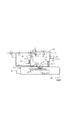
図1において、8はEUV光、1はレチクル照明ミラー、2は投影系第1ミラー、3は投影系第2ミラー、4は投影系第3ミラー、5は投影系第4ミラー、6は投影系第5ミラー、7は投影系第6ミラー、11は反射型レチクル、12はレチクル保持装置、13はレチクルステージ、14はレチクルアライメント光学系、21はウエハ、22はウエハチャック、23はウエハステージ、24はウエハアライメント光学系を示す。 In FIG. 1, 8 is EUV light, 1 is a reticle illumination mirror, 2 is a projection system first mirror, 3 is a projection system second mirror, 4 is a projection system third mirror, 5 is a projection system fourth mirror, and 6 is a projection. System fifth mirror, 7 is a projection system sixth mirror, 11 is a reflective reticle, 12 is a reticle holding device, 13 is a reticle stage, 14 is a reticle alignment optical system, 21 is a wafer, 22 is a wafer chuck, and 23 is a wafer stage. , 24 denotes a wafer alignment optical system.
EUV光源には、不図示のレーザープラズマ光源が用いられる。これは真空容器外に置かれたターゲット供給装置により供給されたターゲット材に励起用パルスレーザーから発生する高強度のパルスレーザー光を照射し、高温のプラズマを発生させ、これから放射される例えば波長13nm程度のEUV光を利用するものである。ターゲット材としては、金属薄膜、不活性ガス、液滴などが用いられ、ガスジェット等の手段で真空容器内に供給される。放射されるEUV光の平均強度を高くするためにはパルスレーザーの繰り返し周波数は高い方が良く、通常数kHzの繰り返し周波数で運転される。
A laser plasma light source (not shown) is used as the EUV light source. This is because a target material supplied by a target supply device placed outside a vacuum vessel is irradiated with high-intensity pulsed laser light generated from a pulse laser for excitation to generate high-temperature plasma and emitted from this, for example,
不図示の照明光学系は、複数の多層膜または斜入射ミラーとオプティカルインテグレータ等から構成され、レチクルを均一に所定の開口数で照明する。 An illumination optical system (not shown) includes a plurality of multilayer films or oblique incidence mirrors, an optical integrator, and the like, and uniformly illuminates the reticle with a predetermined numerical aperture.
投影光学系は複数のミラーを用いている。ミラー枚数は少ない方がEUV光の利用効率が高いが、収差補正が難しくなる。収差補正に必要なミラー枚数は4枚から6枚程度である。ミラーの反射面の形状は凸面または凹面の球面または非球面である。開口数NAは0.1〜0.2程度である。 The projection optical system uses a plurality of mirrors. Although the use efficiency of EUV light is higher when the number of mirrors is smaller, aberration correction becomes difficult. The number of mirrors necessary for aberration correction is about 4 to 6. The shape of the reflecting surface of the mirror is a convex or concave spherical or aspherical surface. The numerical aperture NA is about 0.1 to 0.2.
ミラーは低膨張率ガラスやシリコンカーバイド等の剛性・硬度が高く、熱膨張率が小さい材料からなる基板を、研削・研磨して所定の反射面形状を創生した後、反射面にモリブデン/シリコンなどの多層膜を成膜したものである。 The mirror is made of a material with high rigidity and hardness, such as low expansion glass or silicon carbide, and a substrate made of a material with a low coefficient of thermal expansion. A multilayer film such as is formed.
レチクルステージ13とウエハステージ23は縮小倍率に比例した速度比で同期して走査する機構をもつ。ここでレチクル又はウエハ面内で走査方向をX、それに垂直な方向をY、レチクル又はウエハ面に垂直な方向をZとする。
The
レチクル11は、レチクルステージ13上のレチクルチャック12に保持される。レチクルステージ13はX方向に高速移動する機構をもつ。また、X方向、Y方向、Z方向、および各軸の回りの回転方向に微動機構をもち、レチクル11の位置決めができるようになっている。レチクルステージ13の位置と姿勢は不図示のレーザ干渉計によって計測され、その結果に基づいて位置と姿勢が制御される。
The reticle 11 is held by the
ウエハ21はウエハチャック22によってウエハステージ23に保持される。ウエハステージ23はレチクルステージ13と同様にX方向に高速移動する機構をもつ。また、X方向、Y方向、Z方向、および各軸の回りの回転方向に微動機構をもち、ウエハ21の位置決めができるようになっている。ウエハステージ23の位置と姿勢は不図示のレーザ干渉計によって計測され、その結果に基づいて位置と姿勢が制御される。
The
アライメント検出機構14によってレチクルの位置と投影光学系の光軸との位置関係、およびウエハの位置と投影光学系の光軸との位置関係が計測され、レチクルの投影像がウエハの所定の位置に一致するようにレチクルステージ13およびウエハステージ23の位置と角度が設定される。
The
また、フォーカス位置検出機構24によってウエハ面でZ方向のフォーカス位置が計測され、ウエハステージの位置及び角度を制御することによって、露光中は常時ウエハ面を投影光学系による結像位置に保つ。
Further, the focus position in the Z direction is measured on the wafer surface by the focus
ウエハ21上で1回のスキャン露光が終わると、ウエハステージ23はX,Y方向にステップ移動して次の走査露光開始位置に移動し、再びレチクルステージ13及びウエハステージ23が投影光学系の縮小倍率に比例した速度比でX方向に同期走査する。
When one scan exposure is completed on the
このようにして、レチクルの縮小投影像がウエハ上に結像した状態でそれらを同期走査するという動作が繰り返される(ステップ・アンド・スキャン)。こうして、ウエハ全面にレチクルの転写パターンが転写される。 In this manner, the operation of synchronously scanning the reduced projection image of the reticle formed on the wafer is repeated (step-and-scan). Thus, the reticle transfer pattern is transferred onto the entire wafer surface.
ここで、露光装置内は露光光を通過するための開口を有する隔壁や絞りなどを使用し、空間的に差圧を生じさせることが可能な構成になっている。 Here, the inside of the exposure apparatus is configured such that a differential pressure can be generated spatially by using a partition wall or an aperture having an opening for passing exposure light.
(レチクルステージと第1光路空間)
まず、レチクル及びレチクルステージを囲むレチクルステージ空間91と投影光学系の第1〜3ミラーを囲む第1光路空間92との間には、遮蔽部材(隔壁)61を設けている。この隔壁は、レチクルを照明する照明光やレチクルから出射する露光光やアライメント光を通過するための開口を有している。ここで、レチクルステージ空間91と第1光路空間92の間の、ガスの行き来が可能な隙間(実施例では、遮蔽部材とレチクル面との間の隙間が1mm以下になるようにしている)を1mm以下として、レチクル空間と第1光路空間との間に差圧を発生させている。ここでは、第1光路空間の圧力がレチクル空間の圧力よりも高くなるようにしている。
(Reticle stage and first optical path space)
First, a shielding member (partition wall) 61 is provided between the
具体的には、レチクルステージ空間91はターボ分子ポンプなどの排気装置31が接続され所定の圧力に保つことができ、空間内の圧力を圧力センサS3でモニタできるよう構成されている。また、第1光路空間92は排気装置32,33が接続され所定の圧力に保つことができ、空間内の圧力を圧力センサS1でモニタできるよう構成されている。このような構成にすることで、レチクルステージ空間と第1光路空間91の間に差動排気系を構成し、レチクルステージ空間91から発生するアウトガスの第1光路空間92への進入量を抑えることが可能である。ここでは排気装置を2つ設けたが、勿論排気装置は1つであっても構わないし、3つ以上設けても構わない。
Specifically, the
(第1光路空間と第2光路空間)
次に、第1光路空間92と第2光路空間93との間にも、前述の遮蔽部材に相当する、絞り部材62が設けられている。この絞り部材62は、レチクルから出射して第1光路空間92を経た露光光の第1光路空間からの出口及び第2光路空間93への入り口を形成している。さらに、この絞り部材62の開口によって、第1光路空間と第2光路空間とを接続することにより、両空間の間に差圧を発生させている。また、第2光路空間には、ゲートバルブGV1を介して排気装置34、及び、ゲートバルブGV2を介して排気装置35が接続され、光路空間93の圧力は圧力センサS2でモニタされている。ここでは、これらの圧力センサからの検出結果及び排気装置等を用いて、第1光路空間92の圧力が第2光路空間93の圧力よりも低くなるようにしている。
(First optical path space and second optical path space)
Next, a
ここで、第2光路空間93にはクライオ冷凍機41、42に接続されたクライオパネル43、44が配置される。ここで、クライオパネルとは、第2光路空間内部の温度より低い温度(好ましくは40Kから200Kの間)に設定された部材であり、第2光路空間内に浮遊している物質を吸着する機能を有している。また、チャンバとミラーがクライオパネル43、44により輻射冷却されるのを抑えるために、輻射シールド51、52、53、54を備える。輻射シールド51は投影系第6ミラー7の冷却を抑えるためにミラーを囲むように配置される。輻射シールド52は投影系第5ミラー6の冷却を抑えるためにミラーを囲むように配置される。輻射シールド53、54はチャンバの冷却を抑えるために配置されている。ここで、クライオパネルを用いてミラーを冷却するように構成しても構わない。その場合は、ミラーの温度を検出する温度センサ(好ましくは非接触で検出する)からの検出結果に基づいて、輻射シールドかクライオパネルの少なくとも一方の温度を調節するように構成するのが好ましい。
Here, cryopanels 43 and 44 connected to the
また、光路空間92、93には窒素やヘリウムなどの不活性ガスを供給するためのガス供給装置を備えており、そのガス供給装置のバルブV1、V2,V3を備え、必要に応じてバルブV4により窒素とヘリウムの供給を切り替えることが可能である。この不活性ガス供給用のバルブは、各光路空間に1つずつであっても構わないし、複数ずつ設けても構わないし、もしくは第1光路空間92にのみ設けるように構成しても構わないし、もしくは第2光路空間93にのみ設けるように構成しても構わない。また、窒素やヘリウムに限らず、アルゴンやクリプトン等のガスを供給するように構成しても構わない。
The
この場合、温度制御はヒータなどの発熱手段を輻射シールドかクライオパネルの少なくともどちらか一方に接続し、温度を調節するように構成しても良いし、また、クライオ冷凍機のON/OFFにより温度を調節するように構成しても良い。 In this case, the temperature control may be configured such that a heating means such as a heater is connected to at least one of the radiation shield and the cryopanel and the temperature is adjusted, or the temperature is controlled by turning on / off the cryocooler. You may comprise so that it may adjust.
また、輻射シールド53、54はクライオパネルからチャンバが冷却されるのを抑えるために露光装置の設置される外部雰囲気と同じ温度に設定にするのが好ましく、輻射シールド51、52は輻射シールド53、54よりも低い温度に設定することで、露光光によるミラー6、7の温度上昇を抑えることが可能である。このようにクライオパネルからの輻射冷却を利用して露光光による光学部品の発熱を抑えるために、輻射シールドごとに異なった温度設定を行っても構わない。
The radiation shields 53 and 54 are preferably set to the same temperature as the external atmosphere in which the exposure apparatus is installed in order to prevent the chamber from being cooled from the cryopanel. By setting the temperature lower than 54, it is possible to suppress the temperature rise of the
(第2光路空間とウエハステージ空間)
また、第2光路空間93とウエハステージ空間94は露光光を通過させるための開口を有する隔壁52により差圧を発生させ、ウエハステージ空間94には排気装置36が接続され、ステージ空間94内の圧力は圧力センサS4によりモニタされる。ここで、第2光路空間とウエハステージ空間との間の、ガスの行き来が可能な開口を有するのは、輻射シールドを兼ねる隔壁52である必要は無く、輻射シールドとは別体で遮蔽部材61のような部材を設けても良い。
(Second optical path space and wafer stage space)
Further, the second
次に、図2に光路空間93とウエハステージ空間94を拡大した図を示す。
Next, FIG. 2 shows an enlarged view of the
ウエハステージ空間94で発生するアウトガス(汚染物質)はレチクルステージ空間91同様、差動排気により、抑制することは可能であるが、露光時にウエハ面上のレジストから発生するコンタミネーション(汚染物質)を抑制することができない。そこで、バルブV4でヘリウムガスを選択し、バルブV1、V2から第2光路空間93にヘリウムガスを供給する。バルブV1、V2を介して供給されるヘリウムは第2光路空間93内に配置された輻射シールド51と投影系第6ミラー7で囲まれた空間と輻射シールド52と投影系第5ミラー6で囲まれた空間に供給され、ミラー近傍で最もヘリウム濃度が高くなるように構成される。
Outgas (contaminant) generated in the
第2光路空間93に供給されたヘリウムは絞り部材62を介して第1光路空間92及び輻射シールド52を介してウエハステージ空間94に噴出される。この時、第2光路空間93内の圧力は0.1〜10Paで制御することで、露光時にウエハ面上から発生するコンタミネーションが第2露光空間や第1露光空間に進入するのを抑制することが可能である。
The helium supplied to the second
また、第2光路空間93で使用されるクライオパネルの温度は100K程度に制御されており、第2光路空間内に浮遊する物質を吸着することから、略排気系のような機能を果たしている。100K程度のクライオパネルを使用することで、融点の低いヘリウムは第2光路空間93でクライオパネルに吸着されることはないが、第2光路空間に進入したわずかなコンタミネーションはクライオパネルに吸着することができる。つまり、ヘリウムの消費量を抑えつつ、コンタミネーションのミラー等への付着を抑制することが可能である。なお、排気装置34、35に接続されたゲートバルブGV1,GV2を閉じて露光を行う。但し、露光光の光路上を安定した状態に保つために、若干の排気及び/又は給気を行うようにしても構わない。
Further, the temperature of the cryopanel used in the second
ここで、第1光路空間92、第2光路空間93、ウエハステージ空間94の圧力をそれぞれ、Por,Pow,Pwとした時、以下の関係を満たすように構成する。
Pow>Por,Pw (条件式1)
ここで、より好ましくは、
Pow>Pw>Por (条件式2)
を満たすように構成する。投影光学系を光の通過順にレチクル側から第1光路空間、第2光路空間とし、ウエハステージを囲む空間をウエハステージ空間としたときに、上記の(条件式1)や(条件式2)のような圧力の関係を満たしつつ露光を行うことにより、ウエハ表面(レジスト)から発生したコンタミネーションがミラー表面に付着するのを抑制することが可能となる。
Here, when the pressures in the first
Pow> Por, Pw (Condition 1)
Here, more preferably,
Pow>Pw> Por (Condition 2)
Configure to meet. When the projection optical system is a first optical path space and a second optical path space from the reticle side in the order of passage of light, and a space surrounding the wafer stage is a wafer stage space, the above (conditional expression 1) and (conditional expression 2) By performing exposure while satisfying such a pressure relationship, it is possible to suppress the contamination generated from the wafer surface (resist) from adhering to the mirror surface.
このような関係を満たすことにより、ウエハステージ空間94で発生するアウトガス及びウエハの露光領域から露光時に発生するコンタミネーションの第2光路空間93への進入を抑えると共に第1光路空間92の圧力上昇を抑えることが可能である。
By satisfying such a relationship, the outgas generated in the
(クライオパネルの再生)
また、クライオパネルはその表面に吸着した分子の蓄積量が多くなるにつれ、吸着(排気)速度が遅くなるために、定期的な再生を必要とする。対策なしで、クライオパネルを再生した場合(クライオパネルの温度を上げて、吸着されていた物質を拡散させてしまった場合)、クライオパネルに吸着していた物質(チャンバ内に存在した水分や各種部材から発生したアウトガスや先に述べたウエハ面上から発生したコンタミネーション)が第2光路空間内に拡散してしまい、それらがミラーに吸着する恐れがある。このように、クライオパネル再生時に発生するガスがミラー表面で吸着されることになり、クライオパネル再生後、所定の圧力レベルまで減圧するのに時間を要するためスループットの低下につながると共に、炭素系化合物や水分などがミラーに吸着した状態で露光を開始することはミラー表面の酸化やミラーの反射率低下につながる。そのため、クライオパネルの再生時の対策を図3を用いてその内容を説明する。
(Reproduction of cryopanel)
Also, the cryopanel requires periodic regeneration because the adsorption (exhaust) speed decreases as the amount of molecules adsorbed on the surface increases. If the cryopanel is regenerated without taking any measures (if the temperature of the cryopanel is raised and the adsorbed material is diffused), the material adsorbed on the cryopanel (moistures in the chamber and various The outgas generated from the member and the contamination generated from the wafer surface described above) may diffuse into the second optical path space and be adsorbed by the mirror. In this way, the gas generated at the time of cryopanel regeneration is adsorbed on the mirror surface, and it takes time to depressurize to a predetermined pressure level after regeneration of the cryopanel. Starting the exposure in a state where water or moisture is adsorbed on the mirror leads to oxidation of the mirror surface and reduction of the mirror reflectivity. Therefore, the content of the countermeasure at the time of reproducing the cryopanel will be described with reference to FIG.
バルブV4により窒素を選択し、V3を介して第1光路空間92に窒素を供給する。また、バルブV2、V1を介して輻射シールド51と投影系第6ミラーで囲まれた空間と輻射シールド52と投影系第5ミラー6で囲まれた空間に窒素を供給する。そして、排気装置34、35を動作させた状態で、ゲートバルブGV1、GV2を開け、各空間の圧力が以下の関係を満たすよう制御する。
Por>Pow,Pw (条件式3)
より好ましくは、
Por>Pow>Pw (条件式4)
を満足するようにする。
Nitrogen is selected by the valve V4, and nitrogen is supplied to the first
Por> Pow, Pw (Condition 3)
More preferably,
Por>Pow> Pw (Condition 4)
To be satisfied.
その後、クライオパネル43、44の再生を開始する。 Thereafter, reproduction of the cryopanels 43 and 44 is started.
上記条件を満たしつつ、光路空間92,93の圧力を1〜100Pa程度で制御することで、再生時にクライオパネル43,44から発生するガスの大部分は排気装置34、35で排気されることになり、投影光学系第5ミラー6、投影系第6ミラー7近傍への拡散を抑え、ミラー表面への吸着を抑えると共に、光路空間92への拡散を抑え、ウエハステージ空間94で発生するアウトガスが光路空間93に進入するのを抑制することが可能になる。この際、第2光路空間内のミラー表面近傍にあるバルブ(ガス給気口)からガスを第2光路空間内にガスを供給するように構成すれば、ミラー近傍が第2光路空間内のガスの流れの最上流になるため、クライオパネルから拡散する物質がミラー表面に付着することをさらに抑制することができる。
By controlling the pressure of the
また、本実施例ではレチクルステージ空間のアウトガスの抑制方法として差動排気を説明したが、ウエハステージ空間同様の対策をレチクルステージ空間91と第1光路空間92の間に施しても、光路空間全体の圧力が上昇するために露光光の透過率が減少するもののレチクルステージ空間に存在するアウトガスの光路空間92への進入を差動排気と同様に抑制することは可能である。
In the present embodiment, the differential exhaust is described as a method for suppressing outgas in the reticle stage space. However, even if a countermeasure similar to that for the wafer stage space is applied between the
また、露光時にはヘリウムを供給し、クライオパネル再生時には窒素を供給するというようにガスの切り替えを行っているが、ヘリウムだけというような1種類のガスだけを使用しても良いし、アルゴンや水素などのEUV光に対し透過率の高いガスを使用しても良い。 In addition, gas is switched such that helium is supplied during exposure and nitrogen is supplied during cryopanel regeneration, but only one type of gas such as helium may be used, or argon or hydrogen. For example, a gas having a high transmittance with respect to EUV light may be used.
また、クライオパネルにより投影光学系が有するミラーが冷却されるのを抑制する輻射シールドを、ヒータなどを用いて温調することにより、クライオパネルのミラー(或いはチャンバ)への輻射冷却の影響を更に抑えることは可能である。 Further, by adjusting the temperature of the radiation shield that suppresses the cooling of the mirror included in the projection optical system by the cryopanel using a heater or the like, the effect of radiation cooling on the mirror (or chamber) of the cryopanel is further increased. It is possible to suppress it.
また、本実施例はクライオパネルとガス(の差圧)による抑制を併用した方式であるが、露光時にガスを供給しない状態でクライオパネルを使用しても、ウエハ等から発生するコンタミネーションのミラーへの付着を抑制することができる。また、本方式のクライオパネルの再生方法により、クライオパネル再生時のミラーの汚染を防止することが可能である。すなわち、第2光路空間93内に配置されたクライオパネル43(44)と、そのクライオパネルによって、投影系のミラー6(7)が(過度に)輻射冷却されないようにする輻射シールド部材52(51)と、第2光路空間93にガスを供給するガス供給装置とを有しており、その供給装置により第2光路空間93にガスが供給される給気口が、輻射シールド部材52(51)よりミラー6側に設けられているように構成すると、クライオパネルの再生時に投影系のミラーに汚染物質が付着することを抑制しつつ、クライオパネルを再生させることが可能となる。
In this embodiment, the cryopanel and the suppression by gas (differential pressure) are used together. However, even if the cryopanel is used without supplying gas at the time of exposure, a contamination mirror generated from a wafer or the like. Adhesion to can be suppressed. Further, the method of reproducing the cryopanel of this system can prevent the mirror from being contaminated when the cryopanel is reproduced. That is, the cryopanel 43 (44) disposed in the second
また、クライオパネルを用いずに、各空間ごとの差圧を使って、コンタミネーションがミラーに付着するのを抑制しても構わない。 Further, without using a cryopanel, it is possible to suppress the adhesion of contamination to the mirror by using a differential pressure for each space.
(実施例2)
第二の実施例の構成を図4に示す。図4は投影系第5ミラー6の近傍を拡大した図であり、本実施例では投影系第5ミラー6の右側に露光光を通過するための開口を有すると共に、周辺に輻射シールドを有するクライオパネルを配置したものである。第1の実施例同様に、露光時、及び、クライオパネル再生時にはガスを供給する。
(Example 2)
The configuration of the second embodiment is shown in FIG. FIG. 4 is an enlarged view of the vicinity of the projection system fifth mirror 6. In this embodiment, the cryo system has an opening for passing exposure light on the right side of the projection system fifth mirror 6 and a radiation shield around it. A panel is arranged. As in the first embodiment, gas is supplied during exposure and during cryopanel regeneration.
ウエハ面上の露光領域上部にクライオパネル45を配置することで、拡散によって光路空間93に進入しようとするコンタミネーション(汚染物質)の軌道がバルブV1を介して供給されるヘリウムにより曲げられ、コンタミネーションがクライオパネル45に衝突し、クライオパネルに吸着される(排気される)確率が高くなる。
By disposing the
この効果を熱流体シミュレーションにより解析した結果を図5に示す。図5は横軸に第2光路空間93の絶対圧力を示し、縦軸に露光時にウエハ面上から発生し、第2光路空間93に進入するコンタミネーション(CxHy)の分圧を示したグラフである。#1(○印)はクライオパネルを動作させずヘリウムのみを供給した場合の結果であり、#2(塗りつぶし□印)はクライオパネル43、44を動作させると共にヘリウムを供給した場合の結果であり、#3(×印)はクライオパネル43、44、45動作させると共にヘリウムを供給した場合の結果である。なお、ヘリウムを供給しない場合にはおよそCxHyの分圧は1E−4Pa程度であった。この結果からもわかるように#1の条件に対し、#2、#3の結果がより低い圧力においてウエハから発生するコンタミネーションのミラーへの付着を抑制する効果を得ることが可能であることが理解できる。
The result of analyzing this effect by thermal fluid simulation is shown in FIG. FIG. 5 is a graph showing the absolute pressure of the second
このようにして、実施例1に対してより少ないヘリウムの供給量で、同程度の抑制効果を得ることが可能である。 In this way, it is possible to obtain the same degree of suppression effect with a smaller supply amount of helium than in the first embodiment.
また、先の実施例では輻射シールドでミラーを囲むように配置したが、図6に示すように通常のクライオポンプのようにクライオパネルを取り囲むように輻射シールド56、57を配置し、投影系第5ミラー6、投影系第6ミラー7にヘリウムを供給する構成にしても良い。この場合、輻射シールドによりクライオパネルが囲まれるため、クライオパネルの排気速度が遅くなるものの、ヘリウムのみを供給する場合に比べ、第2光路空間93内の炭素化合物の分圧をより低く抑えることが可能である。この輻射シールド56、57は、複数の板状部材を有しており、それらの板状部材の形状は、図6のようにそれぞれが折り曲がっている必要は無く、それぞれの断面は直線状や曲線状であっても構わない。
In the previous embodiment, the mirror is surrounded by the radiation shield. However, as shown in FIG. 6, the radiation shields 56 and 57 are disposed so as to surround the cryopanel as in a normal cryopump. Helium may be supplied to the five mirrors 6 and the projection system
また、この場合、クライオパネルの再生時にはミラーを囲むカバーの役目をしていた輻射シールドがないために、ミラー表面にヘリウムを供給しても、クライオパネルから発生する汚染物質を含むガスに対して高い抑制効果を得ることはできない。そのため、図7に示すように、輻射シールド57、58の内側に排気用の流路を設け、再生時にはバルブV7、V8を開けることで、輻射シールドで囲まれた空間からガスを排気する装置37、38を配置することが望ましい。このように、排気装置37、38によって、第2光路空間93内の窒素を排気するように構成することで、ミラー近傍でのクライオパネルから放出された汚染物質の濃度の上昇を抑えることが可能である。
Also, in this case, since there is no radiation shield that served as a cover surrounding the mirror when the cryopanel was regenerated, even if helium was supplied to the mirror surface, the gas containing contaminants generated from the cryopanel A high suppression effect cannot be obtained. Therefore, as shown in FIG. 7, a
また、本実施例においても、輻射シールドをヒータなどにより温調することにより、クライオパネルのミラーへの輻射冷却の影響を更に抑えることは可能である。 Also in this embodiment, it is possible to further suppress the influence of radiation cooling on the mirror of the cryopanel by adjusting the temperature of the radiation shield with a heater or the like.
また、本実施例はクライオパネルとガスによる抑制を併用した方式であるが、露光時にクライオパネルのみを使用した方式であっても、本方式のクライオパネルの再生方法により、クライオパネル再生時のミラーの汚染を防止することが可能である。すなわち、第2光路空間93内に配置されたクライオパネル43(44)と、第2光路空間内でそのクライオパネルを含む空間を形成する部材54、57(53、56)と、そのクライオパネルを含む空間内に排気口を有し、この排気口から排気する排気装置とを有するような構成にすれば、クライオパネルの再生時に投影系のミラーに汚染物質が付着することを抑制することができる。
In addition, this embodiment is a method that uses both suppression by a cryopanel and gas, but even when using only a cryopanel at the time of exposure, the reproducing method of the cryopanel of this method makes it possible to use a mirror when reproducing the cryopanel. It is possible to prevent contamination. That is, a cryopanel 43 (44) arranged in the second
また、図11に示すようにウエハステージ空間94内にクライオ冷凍機48に接続されたクライオパネル47を配置し、クライオパネルを取り囲むように輻射シールド59、60を配置しても構わない。その場合、不図示の輻射シールドの温度を検出する温度センサからの検出結果に基づいて、輻射シールド59、60、またはクライオパネル47の少なくともどちらか一方の温度を調節するように構成するのが好ましい。また、温度制御はヒータなどの発熱手段を輻射シールドかクライオパネルの少なくともどちらか一方に接続し、温度を調節するように構成しても良いし、また、クライオ冷凍機のON/OFFにより温度を調節するように構成しても良い。
Further, as shown in FIG. 11, a cryopanel 47 connected to the cryocooler 48 may be disposed in the
輻射シールド59,60はクライオパネルからウエハ、チャンバやステージが冷却されるのを抑えるために露光装置の設置される外部雰囲気と同じ温度に設定にするのが好ましい。また同様にレチクルステージ空間に同様の構成を配置しても構わない。このような構成にすることで、各ステージ空間内の各構成部材から発生するコンタミネーションの分圧を一桁程度下げることが可能である。 The radiation shields 59 and 60 are preferably set to the same temperature as the external atmosphere in which the exposure apparatus is installed in order to suppress the cooling of the wafer, chamber and stage from the cryopanel. Similarly, a similar configuration may be arranged in the reticle stage space. By adopting such a configuration, it is possible to reduce the partial pressure of contamination generated from each component in each stage space by about one digit.
また、本実施例においては、EUV光を用いて露光を行っているが、EUV光に限らず、真空中もしくは高真空中で露光を行う露光装置になら、本実施例は適用可能である。また、波長0.5nm〜20nmの極端紫外光を用いて露光を行う露光装置にも好適である。また、クライオパネル以外でコールドトラップを用いて、露光装置中のコンタミネーションを除去する方法を用いた場合にも、本実施例は適用可能である。 In the present embodiment, the exposure is performed using EUV light. However, the present embodiment is not limited to EUV light, but can be applied to any exposure apparatus that performs exposure in a vacuum or high vacuum. It is also suitable for an exposure apparatus that performs exposure using extreme ultraviolet light having a wavelength of 0.5 nm to 20 nm. In addition, this embodiment can also be applied to a case where a method other than the cryopanel for removing contamination in the exposure apparatus using a cold trap is used.
また、本実施例1,2においては、投影光学系の光学素子を囲むチャンバを2つの空間(第1光路空間と第2光路空間、もしくはレチクル側チャンバとウエハ側チャンバ)に分けたが、勿論チャンバ内を3つ以上の空間に分離しても構わない。その場合、クライオパネル(コールドトラップ)を配置するのは、最もウエハに近い空間であるのが好ましい。 In the first and second embodiments, the chamber surrounding the optical element of the projection optical system is divided into two spaces (a first optical path space and a second optical path space, or a reticle side chamber and a wafer side chamber). The inside of the chamber may be divided into three or more spaces. In that case, the cryopanel (cold trap) is preferably disposed in the space closest to the wafer.
また、クライオパネルを投影光学系の最下面(最もウエハステージに近い面)に配置するようにしても良い。但し、その場合はウエハが輻射冷却により過度に冷却されてしまわないように、クライオパネルとウエハとの間に輻射シールドを設けるようにするのが望ましい。 Further, the cryopanel may be disposed on the lowermost surface (the surface closest to the wafer stage) of the projection optical system. In this case, however, it is desirable to provide a radiation shield between the cryopanel and the wafer so that the wafer is not excessively cooled by the radiation cooling.
本実施例によれば、光路空間内にクライオパネルを使用することによりヘリウムなどのEUV光に対し透過率の高いガスでウエハ面上から発生する炭素化合物の抑制する場合に、より低い圧力で所望の抑制効果を得ることが可能になるため、圧力上昇に伴うEUV露光光の透過率低下を抑え、高いスループットを維持することが可能である。 According to the present embodiment, when a cryopanel is used in the optical path space, the carbon compound generated from the wafer surface is suppressed with a gas having a high transmittance with respect to EUV light such as helium, and the desired pressure can be obtained at a lower pressure. Therefore, it is possible to suppress a decrease in the transmittance of the EUV exposure light accompanying an increase in pressure and maintain a high throughput.
また、抑制ガスの供給量を抑えることができるため、ランニングコストを削減することが可能である。 In addition, since the supply amount of the suppression gas can be suppressed, the running cost can be reduced.
また、クライオパネルの再生時に蓄積したガスがミラー近傍に拡散するのを抑えることで、ミラーの汚染を抑えることが可能である。 Further, it is possible to suppress the contamination of the mirror by suppressing the gas accumulated during the regeneration of the cryopanel from diffusing near the mirror.
次に、図9及び図10を参照して、上述の露光装置を利用したデバイス製造方法の実施例3を説明する。 Next, a third embodiment of the device manufacturing method using the above-described exposure apparatus will be described with reference to FIGS.
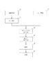
図9は、デバイス(ICやLSIなどの半導体チップ、LCD、CCD等)の製造を説明するためのフローチャートである。本実施形態においては、半導体チップの製造を例に説明する。ステップ1(回路設計)では、デバイスの回路設計を行う。ステップ2(マスク製作)では、設計した回路パターンを形成したマスクを製作する。ステップ3(ウエハ製造)では、シリコンなどの材料を用いてウエハを製造する。ステップ4(ウェハプロセス)は、前工程と呼ばれ、マスクとウエハを用いてリソグラフィー技術によってウエハ上に実際の回路を形成する。ステップ5(組み立て)は、後工程と呼ばれ、ステップ4によって作成されたウエハを用いて半導体チップ化する工程であり、アッセンブリ工程(ダイシング、ボンディング)、パッケージング工程(チップ封入)等の工程を含む。ステップ6(検査)では、ステップ5で作成された半導体デバイスの動作確認テスト、耐久性テストなどの検査を行う。こうした工程を経て半導体デバイスが完成し、それが出荷(ステップ7)される。
FIG. 9 is a flowchart for explaining how to fabricate devices (ie, semiconductor chips such as IC and LSI, LCDs, CCDs, and the like). In the present embodiment, the manufacture of a semiconductor chip will be described as an example. In step 1 (circuit design), a device circuit is designed. In step 2 (mask production), a mask on which the designed circuit pattern is formed is produced. In step 3 (wafer manufacture), a wafer is manufactured using a material such as silicon. Step 4 (wafer process) is called a pre-process, and an actual circuit is formed on the wafer by lithography using the mask and wafer. Step 5 (assembly) is called a post-process, and is a process for forming a semiconductor chip using the wafer created in
図10は、ステップ4のウェハプロセスの詳細なフローチャートである。ステップ11(酸化)では、ウエハの表面を酸化させる。ステップ12(CVD)では、ウエハの表面に絶縁膜を形成する。ステップ13(電極形成)では、ウエハ上に電極を蒸着などによって形成する。ステップ14(イオン打ち込み)では、ウエハにイオンを打ち込む。ステップ15(レジスト処理)では、ウエハに感光剤を塗布する。ステップ16(露光)では、露光装置200によってマスクの回路パターンをウエハに露光する。ステップ17(現像)では、露光したウエハを現像する。ステップ18(エッチング)では、現像したレジスト像以外の部分を削り取る。ステップ19(レジスト剥離)では、エッチングが済んで不要となったレジストを取り除く。これらのステップを繰り返し行うことによってウエハ上に多重に回路パターンが形成される。本実施形態のデバイス製造方法によれば、従来よりも高品位のデバイスを製造することができる。このように、露光装置を使用するデバイス製造方法、並びに結果物としてのデバイスも本発明の一側面を構成する。
FIG. 10 is a detailed flowchart of the wafer process in
以上、本発明の好ましい実施例について説明したが、本願実施例は、実施例1及び2及び3を任意に組み合わせても構わない。 As mentioned above, although the preferable Example of this invention was described, Example of this application may combine Example 1, 2 and 3 arbitrarily.
Claims (17)
Pow>Pw
の関係を満たしつつ、コールドトラップを再生することを特徴とする請求項10に記載の露光装置。 When the pressure in the wafer side chamber is Pow and the pressure in the space surrounding the stage is Pw,
Pow> Pw
The exposure apparatus according to claim 10, wherein the cold trap is regenerated while satisfying the above relationship.
17. A device manufacturing method comprising: exposing an object to be exposed using the exposure apparatus according to claim 1; and developing the exposed object to be exposed.
Priority Applications (2)
| Application Number | Priority Date | Filing Date | Title |
|---|---|---|---|
| JP2004211693A JP2005101537A (en) | 2003-08-29 | 2004-07-20 | Lithography and method of manufacturing device using same |
| US10/928,527 US7330236B2 (en) | 2003-08-29 | 2004-08-27 | Exposure apparatus, and device manufacturing method using the same |
Applications Claiming Priority (2)
| Application Number | Priority Date | Filing Date | Title |
|---|---|---|---|
| JP2003209519 | 2003-08-29 | ||
| JP2004211693A JP2005101537A (en) | 2003-08-29 | 2004-07-20 | Lithography and method of manufacturing device using same |
Publications (2)
| Publication Number | Publication Date |
|---|---|
| JP2005101537A true JP2005101537A (en) | 2005-04-14 |
| JP2005101537A5 JP2005101537A5 (en) | 2007-08-30 |
Family
ID=34466736
Family Applications (1)
| Application Number | Title | Priority Date | Filing Date |
|---|---|---|---|
| JP2004211693A Withdrawn JP2005101537A (en) | 2003-08-29 | 2004-07-20 | Lithography and method of manufacturing device using same |
Country Status (2)
| Country | Link |
|---|---|
| US (1) | US7330236B2 (en) |
| JP (1) | JP2005101537A (en) |
Cited By (11)
| Publication number | Priority date | Publication date | Assignee | Title |
|---|---|---|---|---|
| JP2006287003A (en) * | 2005-04-01 | 2006-10-19 | Tohoku Univ | Exposure device |
| JP2006303270A (en) * | 2005-04-22 | 2006-11-02 | Nikon Corp | Aligner |
| JP2007194590A (en) * | 2005-11-23 | 2007-08-02 | Asml Netherlands Bv | Radiation system and lithography apparatus |
| JP2007281142A (en) * | 2006-04-05 | 2007-10-25 | Canon Inc | Exposure device and method therefor, and manufacturing method of device |
| EP2000854A2 (en) | 2007-06-04 | 2008-12-10 | Canon Kabushiki Kaisha | Substrate processing apparatus and method of manufacturing device |
| JP2010503980A (en) * | 2006-09-19 | 2010-02-04 | カール・ツァイス・エスエムティー・アーゲー | Optical apparatus, particularly projection exposure apparatus for EUV lithography and reflective optical element with less contamination |
| JP2010129687A (en) * | 2008-11-26 | 2010-06-10 | Nikon Corp | Vacuum apparatus, light source apparatus, exposure apparatus, and method of manufacturing device |
| US8259284B2 (en) | 2008-08-27 | 2012-09-04 | Canon Kabushiki Kaisha | Exposure apparatus and device manufacturing method |
| US8901524B2 (en) | 2009-02-12 | 2014-12-02 | Gigaphoton Inc. | Extreme ultraviolet light source apparatus |
| US9291919B2 (en) | 2010-11-22 | 2016-03-22 | Renesas Electronics Corporation | Light exposure method, and light exposure apparatus |
| JP2020516942A (en) * | 2017-04-11 | 2020-06-11 | エーエスエムエル ネザーランズ ビー.ブイ. | Lithographic apparatus and cooling method |
Families Citing this family (21)
| Publication number | Priority date | Publication date | Assignee | Title |
|---|---|---|---|---|
| US20060127293A1 (en) * | 2004-10-12 | 2006-06-15 | Infineon Technologies Richmond Lp | System and method for processing semiconductor material using radiant energy source |
| US20070085984A1 (en) * | 2005-10-18 | 2007-04-19 | Asml Netherlands B.V. | Lithographic projection apparatus, device manufacturing method and device manufactured thereby |
| TWI330762B (en) * | 2005-03-29 | 2010-09-21 | Asml Netherlands Bv | Seal of a lithographic apparatus, lithographic apparatus, device manufacturing method and data storage medium |
| US7502095B2 (en) * | 2005-03-29 | 2009-03-10 | Asml Netherlands B.V. | Lithographic apparatus, device manufacturing method, and device manufactured thereby |
| EP1981066B1 (en) * | 2006-01-30 | 2014-01-22 | Nikon Corporation | Optical member holding apparatus and exposure apparatus |
| US20080073596A1 (en) * | 2006-08-24 | 2008-03-27 | Asml Netherlands B.V. | Lithographic apparatus and method |
| JP2008263173A (en) * | 2007-03-16 | 2008-10-30 | Canon Inc | Exposure apparatus |
| US8901521B2 (en) * | 2007-08-23 | 2014-12-02 | Asml Netherlands B.V. | Module and method for producing extreme ultraviolet radiation |
| NL1036181A1 (en) * | 2007-11-30 | 2009-06-04 | Asml Netherlands Bv | A lithographic apparatus, a projection system and a device manufacturing method. |
| DE102008000957A1 (en) * | 2008-04-03 | 2009-10-08 | Carl Zeiss Smt Ag | Protection module and EUV lithography device with protection module |
| WO2010013671A1 (en) * | 2008-08-01 | 2010-02-04 | 株式会社ニコン | Exposure method and system, and device manufacturing method |
| DE102009029282A1 (en) | 2009-09-08 | 2011-03-24 | Carl Zeiss Smt Gmbh | Optical arrangement, in particular in a projection exposure apparatus for EUV lithography |
| DE102011080649A1 (en) * | 2010-09-24 | 2012-03-29 | Carl Zeiss Smt Gmbh | Optical arrangement in a microlithographic projection exposure apparatus |
| WO2013156041A1 (en) * | 2012-04-18 | 2013-10-24 | Carl Zeiss Smt Gmbh | A microlithographic apparatus and a method of changing an optical wavefront in an objective of such an apparatus |
| US9389180B2 (en) | 2013-02-15 | 2016-07-12 | Kla-Tencor Corporation | Methods and apparatus for use with extreme ultraviolet light having contamination protection |
| CN103197508B (en) * | 2013-03-06 | 2014-11-12 | 华中科技大学 | Analogue means of optical surface contamination and cleaning under extreme ultraviolet irradiation |
| US10714371B2 (en) * | 2017-11-16 | 2020-07-14 | Taiwan Semiconductor Manufacturing Co., Ltd. | Method and apparatus for lithography in semiconductor fabrication |
| CN108398858B (en) * | 2018-03-20 | 2019-05-10 | 李笛 | A kind of gas isolator and partition method |
| NL2025089A (en) * | 2019-04-01 | 2020-10-06 | Asml Netherlands Bv | A lithographic apparatus and related methods |
| CN112485978A (en) * | 2020-12-24 | 2021-03-12 | 清华大学 | Vacuum degassing device for lithographic apparatus |
| US20220350264A1 (en) * | 2021-04-30 | 2022-11-03 | Taiwan Semiconductor Manufacturing Company, Ltd. | Semiconductor processing tool and methods of operation |
Family Cites Families (34)
| Publication number | Priority date | Publication date | Assignee | Title |
|---|---|---|---|---|
| US3800781A (en) * | 1972-05-30 | 1974-04-02 | K Zalucki | Specimen-taking device |
| US4023559A (en) * | 1975-01-28 | 1977-05-17 | Smith & Nephew (Australia) Pty. Limited | Sampling catheter device |
| IT1126526B (en) * | 1979-12-07 | 1986-05-21 | Enrico Dormia | SURGICAL EXTRACTOR TO REMOVE FOREIGN BODIES THAT ARE FOUND IN THE NATURAL ROUTES OF THE HUMAN BODY, AS CALCULATIONS AND SIMILAR |
| JPS61160934A (en) * | 1985-01-10 | 1986-07-21 | Canon Inc | Projection optical device |
| US4730949A (en) * | 1986-03-24 | 1988-03-15 | The Kendall Company | Surgical scrub brush |
| US4952204A (en) * | 1988-08-10 | 1990-08-28 | Gam-Med Packaging Corporation | Dry handle swab assembly and unit |
| US4980563A (en) * | 1990-01-09 | 1990-12-25 | United States Department Of Energy | VUV lithography |
| JP3212818B2 (en) * | 1994-12-28 | 2001-09-25 | シャープ株式会社 | Electronic cooling device |
| US5877843A (en) * | 1995-09-12 | 1999-03-02 | Nikon Corporation | Exposure apparatus |
| WO2004075970A1 (en) * | 1996-01-24 | 2004-09-10 | Yasuaki Arai | Chemical injecion port |
| JP3695000B2 (en) * | 1996-08-08 | 2005-09-14 | 株式会社ニコン | Exposure method and exposure apparatus |
| JPH1131647A (en) * | 1997-07-11 | 1999-02-02 | Oki Electric Ind Co Ltd | Projection aligner |
| EP1041605A4 (en) * | 1997-08-29 | 2005-09-21 | Nikon Corp | Temperature adjusting method and aligner to which this method is applied |
| US7274430B2 (en) * | 1998-02-20 | 2007-09-25 | Carl Zeiss Smt Ag | Optical arrangement and projection exposure system for microlithography with passive thermal compensation |
| US6364856B1 (en) * | 1998-04-14 | 2002-04-02 | Boston Scientific Corporation | Medical device with sponge coating for controlled drug release |
| US6459472B1 (en) | 1998-05-15 | 2002-10-01 | Asml Netherlands B.V. | Lithographic device |
| US6765647B1 (en) * | 1998-11-18 | 2004-07-20 | Nikon Corporation | Exposure method and device |
| JP2001118783A (en) * | 1999-10-21 | 2001-04-27 | Nikon Corp | Exposure method and device, and device manufacturing method |
| US7094428B2 (en) * | 2000-06-16 | 2006-08-22 | The University Of Medicine And Dentistry Of New Jersey | Hemostatic compositions, devices and methods |
| US6527746B1 (en) * | 2000-08-03 | 2003-03-04 | Ev3, Inc. | Back-loading catheter |
| JPWO2002056332A1 (en) * | 2001-01-10 | 2004-05-20 | 株式会社荏原製作所 | Inspection apparatus using electron beam, inspection method, and device manufacturing method using the inspection apparatus |
| US6599296B1 (en) * | 2001-07-27 | 2003-07-29 | Advanced Cardiovascular Systems, Inc. | Ratcheting handle for intraluminal catheter systems |
| US6702759B2 (en) * | 2001-07-31 | 2004-03-09 | Private Concepts, Inc. | Intra-vaginal self-administered cell collecting device and method |
| US6893431B2 (en) * | 2001-10-15 | 2005-05-17 | Scimed Life Systems, Inc. | Medical device for delivering patches |
| US6856475B2 (en) * | 2001-10-31 | 2005-02-15 | The Furukawa Electric Co., Ltd | Optical module having temperature adjustment features |
| JP3789812B2 (en) * | 2001-12-17 | 2006-06-28 | 三菱電機株式会社 | Space navigation optical instrument and its contaminant removal method |
| US6846086B2 (en) * | 2002-03-11 | 2005-01-25 | Intel Corporation | Mirror assembly with thermal contour control |
| US20040051984A1 (en) * | 2002-06-25 | 2004-03-18 | Nikon Corporation | Devices and methods for cooling optical elements in optical systems, including optical systems used in vacuum environments |
| JP3944008B2 (en) * | 2002-06-28 | 2007-07-11 | キヤノン株式会社 | Reflective mirror apparatus, exposure apparatus, and device manufacturing method |
| EP1387054B1 (en) * | 2002-07-31 | 2012-07-25 | Canon Kabushiki Kaisha | Cooling apparatus for an optical element, exposure apparatus comprising said cooling apparatus, and device fabrication method |
| JP2004128213A (en) * | 2002-10-02 | 2004-04-22 | Canon Inc | Temperature control system and aligner incorporating the same |
| US7390298B2 (en) * | 2003-01-06 | 2008-06-24 | City Of Hope | Expandable surgical retractor for internal body spaces approached with minimally invasive incisions or through existing orifices |
| JP4311711B2 (en) * | 2003-02-24 | 2009-08-12 | キヤノン株式会社 | Exposure apparatus and device manufacturing method |
| US6992306B2 (en) * | 2003-04-15 | 2006-01-31 | Canon Kabushiki Kaisha | Temperature adjustment apparatus, exposure apparatus having the same, and device fabricating method |
-
2004
- 2004-07-20 JP JP2004211693A patent/JP2005101537A/en not_active Withdrawn
- 2004-08-27 US US10/928,527 patent/US7330236B2/en not_active Expired - Fee Related
Cited By (16)
| Publication number | Priority date | Publication date | Assignee | Title |
|---|---|---|---|---|
| JP2006287003A (en) * | 2005-04-01 | 2006-10-19 | Tohoku Univ | Exposure device |
| JP2006303270A (en) * | 2005-04-22 | 2006-11-02 | Nikon Corp | Aligner |
| JP2007194590A (en) * | 2005-11-23 | 2007-08-02 | Asml Netherlands Bv | Radiation system and lithography apparatus |
| US7633597B2 (en) | 2006-04-05 | 2009-12-15 | Canon Kabushiki Kaisha | Exposure method and apparatus, and device manufacturing method |
| JP2007281142A (en) * | 2006-04-05 | 2007-10-25 | Canon Inc | Exposure device and method therefor, and manufacturing method of device |
| KR100917968B1 (en) * | 2006-04-05 | 2009-09-17 | 캐논 가부시끼가이샤 | Exposure method and apparatus, and device manufacturing method |
| JP2010503980A (en) * | 2006-09-19 | 2010-02-04 | カール・ツァイス・エスエムティー・アーゲー | Optical apparatus, particularly projection exposure apparatus for EUV lithography and reflective optical element with less contamination |
| EP2000854A2 (en) | 2007-06-04 | 2008-12-10 | Canon Kabushiki Kaisha | Substrate processing apparatus and method of manufacturing device |
| JP2008300806A (en) * | 2007-06-04 | 2008-12-11 | Canon Inc | Substrate processing apparatus, exposure apparatus, and method of manufacturing device |
| EP2161351A1 (en) | 2007-06-04 | 2010-03-10 | Canon Kabushiki Kaisha | Substrate processing apparatus and method of manufacturing a device |
| US8259284B2 (en) | 2008-08-27 | 2012-09-04 | Canon Kabushiki Kaisha | Exposure apparatus and device manufacturing method |
| JP2010129687A (en) * | 2008-11-26 | 2010-06-10 | Nikon Corp | Vacuum apparatus, light source apparatus, exposure apparatus, and method of manufacturing device |
| US8901524B2 (en) | 2009-02-12 | 2014-12-02 | Gigaphoton Inc. | Extreme ultraviolet light source apparatus |
| US9291919B2 (en) | 2010-11-22 | 2016-03-22 | Renesas Electronics Corporation | Light exposure method, and light exposure apparatus |
| JP2020516942A (en) * | 2017-04-11 | 2020-06-11 | エーエスエムエル ネザーランズ ビー.ブイ. | Lithographic apparatus and cooling method |
| JP7155148B2 (en) | 2017-04-11 | 2022-10-18 | エーエスエムエル ネザーランズ ビー.ブイ. | Lithographic apparatus and cooling method |
Also Published As
| Publication number | Publication date |
|---|---|
| US20050110966A1 (en) | 2005-05-26 |
| US7330236B2 (en) | 2008-02-12 |
Similar Documents
| Publication | Publication Date | Title |
|---|---|---|
| JP2005101537A (en) | Lithography and method of manufacturing device using same | |
| US7423724B2 (en) | Exposure apparatus and device manufacturing method | |
| EP1674932B1 (en) | Lithographic apparatus, illumination system and debris trapping system | |
| JP4487108B2 (en) | Lithographic projection apparatus, gas purge method, device manufacturing method, and purge gas supply system | |
| US7221432B2 (en) | Exposure apparatus | |
| JP4922638B2 (en) | Lithographic apparatus, seal, device manufacturing method, computer program, and data recording medium | |
| JP4378357B2 (en) | Exposure apparatus, pressure control method thereof, and device manufacturing method | |
| US7518132B2 (en) | Light source apparatus, exposure apparatus and device fabrication method | |
| JP3696201B2 (en) | Lithographic apparatus and device manufacturing method | |
| US7050152B2 (en) | Exposure apparatus | |
| TWI390360B (en) | Device manufacturing method and lithographic apparatus | |
| JP2004273864A (en) | Thermostatic vacuum container and exposure device using it | |
| JP2005129898A (en) | Aligner and device manufacturing method | |
| JP2006100363A (en) | Aligner, exposure method, and device manufacturing method | |
| JP2008300806A (en) | Substrate processing apparatus, exposure apparatus, and method of manufacturing device | |
| JP2006222198A (en) | Aligner | |
| TWI422984B (en) | Lithographic apparatus comprising a magnet, method for the protection of a magnet in a lithographic apparatus and device manufacturing method | |
| JP2023519552A (en) | Conduit system, radiation source, lithographic apparatus and method thereof | |
| JP2006173245A (en) | Aligner and process for manufacturing device | |
| US7692762B2 (en) | Exposure apparatus | |
| JP2010267926A (en) | Substrate processing apparatus, and method of manufacturing device | |
| JP2006024849A (en) | Exposure apparatus and manufacturing method of device | |
| JP2003115433A (en) | Exposure method and aligner | |
| JP2005079294A (en) | Exposure device, exposure system, and method for manufacturing device | |
| JP2007142019A (en) | Exposure device |
Legal Events
| Date | Code | Title | Description |
|---|---|---|---|
| A521 | Request for written amendment filed |
Free format text: JAPANESE INTERMEDIATE CODE: A523 Effective date: 20070718 |
|
| A621 | Written request for application examination |
Free format text: JAPANESE INTERMEDIATE CODE: A621 Effective date: 20070718 |
|
| RD04 | Notification of resignation of power of attorney |
Free format text: JAPANESE INTERMEDIATE CODE: A7424 Effective date: 20100201 |
|
| A761 | Written withdrawal of application |
Free format text: JAPANESE INTERMEDIATE CODE: A761 Effective date: 20100216 |
|
| A977 | Report on retrieval |
Free format text: JAPANESE INTERMEDIATE CODE: A971007 Effective date: 20100217 |