JP2005091663A - Drive voltage control method, drive voltage control program, drive voltage control device, and optical transmitter for Mach-Zehnder type optical modulator - Google Patents
Drive voltage control method, drive voltage control program, drive voltage control device, and optical transmitter for Mach-Zehnder type optical modulator Download PDFInfo
- Publication number
- JP2005091663A JP2005091663A JP2003324079A JP2003324079A JP2005091663A JP 2005091663 A JP2005091663 A JP 2005091663A JP 2003324079 A JP2003324079 A JP 2003324079A JP 2003324079 A JP2003324079 A JP 2003324079A JP 2005091663 A JP2005091663 A JP 2005091663A
- Authority
- JP
- Japan
- Prior art keywords
- voltage
- mach
- optical modulator
- drive voltage
- drive
- Prior art date
- Legal status (The legal status is an assumption and is not a legal conclusion. Google has not performed a legal analysis and makes no representation as to the accuracy of the status listed.)
- Pending
Links
Images

Landscapes
- Optical Modulation, Optical Deflection, Nonlinear Optics, Optical Demodulation, Optical Logic Elements (AREA)
Abstract
【課題】 マッハツェンダ型光変調器の駆動電圧の振幅Vppをバイアス電圧Vbによらず自動的に最適値Vπに設定することにより、作業時間の短縮と費用を低減し、伝送される光信号の品質を一定に維持する。
【解決手段】 出力光の平均パワーを検出する光検出部18と、前記光検出部18の出力信号に所定の演算処理を施してマッハツェンダ型光変調器14のバイアス電圧制御信号と駆動電圧制御信号を出力する信号処理部19と、マッハツェンダ型光変調器14にバイアス電圧を印加するバイアス電圧制御部20と、マッハツェンダ型光変調器14に駆動電圧を印加する駆動電圧制御部21とを具備し、前記バイアス電圧を順次変化させたときの前記平均パワーの変動量が所定値以下になる前記駆動電圧を求めた後、前記駆動電圧をデータ信号に従ってマッハツェンダ型光変調器14に印加することによりレーザ光を変調し、この変調されたレーザ光を送出する。
【選択図】 図1PROBLEM TO BE SOLVED: To shorten an operation time and a cost by automatically setting an amplitude Vpp of a drive voltage of a Mach-Zehnder type optical modulator to an optimum value Vπ irrespective of a bias voltage Vb, and quality of a transmitted optical signal Is kept constant.
A light detection unit for detecting an average power of output light, and a bias voltage control signal and a drive voltage control signal for a Mach-Zehnder type optical modulator by performing predetermined arithmetic processing on an output signal of the light detection unit. A signal processing unit 19 that outputs a bias voltage control unit 20 that applies a bias voltage to the Mach-Zehnder optical modulator 14, and a drive voltage control unit 21 that applies a drive voltage to the Mach-Zehnder optical modulator 14. After obtaining the drive voltage at which the fluctuation amount of the average power when the bias voltage is sequentially changed is less than or equal to a predetermined value, the drive voltage is applied to the Mach-Zehnder optical modulator 14 according to the data signal, thereby laser light. Is modulated, and the modulated laser beam is transmitted.
[Selection] Figure 1
Description
本発明は、光送信装置に係わり、特に外部光変調器を用いた光送信装置であって、マッハツェンダ型光変調器の駆動電圧を最適値に設定するのに好適な駆動電圧制御方法、駆動電圧制御プログラム、駆動電圧制御装置および光送信装置に関する。 The present invention relates to an optical transmission device, and more particularly to an optical transmission device using an external optical modulator, and a drive voltage control method and drive voltage suitable for setting the drive voltage of a Mach-Zehnder optical modulator to an optimum value The present invention relates to a control program, a drive voltage control device, and an optical transmission device.
従来の光通信システムに用いられる光送信装置では、入力信号で半導体レーザの駆動電流を変調することにより入力信号を光信号に変換する直接変調方式が用いられていた。しかし、この変調方式では半導体レーザに注入される電流を変化させるため半導体レーザのチャープ特性により、その発振波長が変化する現象が生じる。このような半導体レーザから出力される光信号を長距離伝送すると光ファイバーの波長分散の影響により光信号の波形劣化が生じ、信号特性が劣化する問題がある。 In an optical transmission device used in a conventional optical communication system, a direct modulation method is used in which an input signal is converted into an optical signal by modulating a driving current of a semiconductor laser with the input signal. However, in this modulation method, the current injected into the semiconductor laser is changed, so that the oscillation wavelength changes due to the chirp characteristics of the semiconductor laser. When an optical signal output from such a semiconductor laser is transmitted over a long distance, there is a problem that the waveform of the optical signal is degraded due to the influence of wavelength dispersion of the optical fiber, and the signal characteristics are degraded.
そこで、長距離伝送をおこなう場合に、原理的にチャープ特性による波長変動を起こさないマッハツェンダ型の外部光変調器(以下、MZ型光変調器という)が使用されるようになってきている。 Therefore, in the case of long-distance transmission, a Mach-Zehnder type external optical modulator (hereinafter referred to as an MZ type optical modulator) that does not cause wavelength fluctuation due to chirp characteristics has been used in principle.
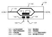
図7はMZ型光変調器の構成を示す図、図8はMZ型光変調器の入出力特性を示す図、図9はMZ型光変調器の駆動電圧の振幅と光出力波形の関係を示す図である。 7 is a diagram showing the configuration of the MZ type optical modulator, FIG. 8 is a diagram showing the input / output characteristics of the MZ type optical modulator, and FIG. 9 is the relationship between the drive voltage amplitude and the optical output waveform of the MZ type optical modulator. FIG.
図7に示すように、MZ型光変調器101は干渉型光変調器の一種で、例えば電気光学効果を有する基板102と、基板102上に設けられた入力光を2つのパスに均等に分岐した後2つのパスを通過した光を合成する光導波路103と、光導波路103中の屈折率を一定量変化させるためのバイアス電圧を印加するバイアス電極104と、同じく光導波路103中の屈折率を入力信号に従って変化させるための駆動電圧を印加する駆動電極105と、接地電極106と、バイアス電圧入力端子107と、駆動電圧入力端子108とで構成されている。
As shown in FIG. 7, the MZ type
即ち、印加された電圧の大きさに応じて2つのパスの光路差を変化させることにより、2つのパスを通過した光を合成して入力信号を光信号に変換するものである。従って、光路差がゼロの時に光出力“1”が得られ、光路差が1/2波長の時に光出力“0”が得られる。 That is, by changing the optical path difference between the two paths according to the magnitude of the applied voltage, the light passing through the two paths is synthesized and the input signal is converted into an optical signal. Accordingly, an optical output “1” is obtained when the optical path difference is zero, and an optical output “0” is obtained when the optical path difference is ½ wavelength.
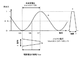
図8に示すように、MZ型光変調器に印加される電圧と光出力との関係は正弦波aの特性を示すので、その動作点を決めるバイアス電圧Vbは特性が最もリニアになる点に設定し、駆動信号bは入力信号の各論理値に対応して光出力の最小値が得られる電圧V0および最大値が得られる電圧V1に設定することにより、消光比(光出力の最大値と最小値の比)の高い光信号cを送信することができる。この電圧V0と電圧V1の差を半波長電圧Vπと呼ぶ。 As shown in FIG. 8, the relationship between the voltage applied to the MZ type optical modulator and the optical output indicates the characteristics of the sine wave a. Therefore, the bias voltage Vb for determining the operating point is the point where the characteristics are most linear. The drive signal b is set to a voltage V0 at which the minimum value of the optical output is obtained and a voltage V1 at which the maximum value is obtained corresponding to each logical value of the input signal. It is possible to transmit an optical signal c having a high ratio (minimum value). The difference between the voltage V0 and the voltage V1 is called a half-wave voltage Vπ.
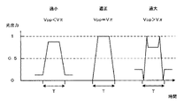
従って、図9に示すように、駆動電圧の振幅Vppが半波長電圧Vπとずれている場合、例えば駆動電圧の振幅Vppが半波長電圧Vπより小さい場合は消光比が低下し、駆動電圧の振幅Vppが半波長電圧Vπより大きい場合は消光比が低下するだけでなく出力光の波形も劣化する。 Therefore, as shown in FIG. 9, when the drive voltage amplitude Vpp deviates from the half-wave voltage Vπ, for example, when the drive voltage amplitude Vpp is smaller than the half-wave voltage Vπ, the extinction ratio decreases, and the drive voltage amplitude When Vpp is larger than the half-wave voltage Vπ, not only the extinction ratio is lowered but also the waveform of the output light is degraded.
従来、駆動電圧の振幅Vppを最適値である半波長電圧Vπに合わせるにはオシロスコープなどを用いてMZ型光変調器から出力される光信号の波形をモニタしながら手作業でMZ型光変調器の駆動回路を調整していた。 Conventionally, in order to adjust the amplitude Vpp of the drive voltage to the optimum half-wave voltage Vπ, the MZ type optical modulator is manually operated while monitoring the waveform of the optical signal output from the MZ type optical modulator using an oscilloscope or the like. The drive circuit was adjusted.
しかしながら、光信号の波形は駆動電圧の振幅Vppとバイアス電圧Vbの両方に依存するのに加えて半波長電圧Vπは入力信号の周波数や温度にも依存するため、光信号の波形を見ただけでは常に最適値Vπに設定するのが難しい。また、一旦装置に組み込んだ後から再調整することも困難である。 However, since the waveform of the optical signal depends on both the amplitude Vpp of the drive voltage and the bias voltage Vb, the half-wave voltage Vπ also depends on the frequency and temperature of the input signal. Therefore, it is difficult to always set the optimum value Vπ. It is also difficult to readjust after being incorporated into the apparatus.
そのため、駆動電圧の振幅Vppを最適値Vπに設定する作業に多大の労力と時間を要するだけでなく、MZ型光変調器や駆動回路の径時変化に起因する駆動電圧の振幅Vppのシフトなどにより伝送される光信号の品質を一定に維持するのが難しいという問題がある。 Therefore, not only a great amount of labor and time is required for the operation of setting the amplitude Vpp of the drive voltage to the optimum value Vπ, but also the shift of the amplitude Vpp of the drive voltage due to a change with time of the diameter of the MZ type optical modulator or the drive circuit, etc. Therefore, there is a problem that it is difficult to maintain the quality of the optical signal transmitted by the transmitter.
これに対して、複数のアナログ信号が多重された1つのRF信号を分岐して得られる第1および第2のRF信号で外部変調される光送信装置において、バイアス電圧VbのDCドリフトによる光信号の平均パワーの変動と歪量の変動を抑制する方法が知られている(例えば、特許文献1参照。)。 On the other hand, in an optical transmitter that is externally modulated by first and second RF signals obtained by branching one RF signal in which a plurality of analog signals are multiplexed, an optical signal due to DC drift of the bias voltage Vb There is known a method for suppressing fluctuations in the average power and distortion amount (see, for example, Patent Document 1).
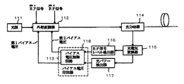
この特許文献1に開示された光送信装置について図を用いて説明する。図10はこの光送信装置の構成を示すブロック図である。
The optical transmission device disclosed in
図10に示すように、光送信装置はレーザ光を出力する光源111と、第1RF信号および第2RF信号が印加されるMZ型光変調器112と、MZ型光変調器112に第1バイアス電圧および第2バイアス電圧を印加するバイアス電圧印加器113と、MZ型光変調器112を通過した光を2つに分岐する光分岐器114と、分岐された一方の光を受光する光電気変換器115と、光電気変換器115の出力よりRF信号レベルを検出するRF信号レベル検出器116と、光パワーを検出する光パワー検出器117と、第1バイアス電圧および第2バイアス電圧を制御するバイアス電圧制御回路118とで構成されている。
As shown in FIG. 10, the optical transmitter includes a
即ち、バイアス電圧制御回路118はMZ型光変調器112から出力される光信号の平均パワーが基準パワーと一致するように第1バイアス電圧をフィードバック制御し、且つ、光信号に含まれるRF信号のレベルが基準レベルと一致するように第2バイアス電圧をフィードバック制御している。
In other words, the bias voltage control circuit 118 feedback-controls the first bias voltage so that the average power of the optical signal output from the MZ type
しかしながら、特許文献1に開示された光送信装置では駆動電圧の振幅Vppが半波長電圧Vπに設定されていることを前提としてバイアス電圧VbのDCドリフトを修正するものであり、駆動電圧の振幅Vppを制御することは困難である。
上述したMZ型光変調器の駆動電圧の振幅Vppを手作業により調整する方法では作業に多大な時間と費用を要するだけでなく、伝送される光信号の品質を一定に維持するのが難しいという問題がある。 The above-described method of manually adjusting the amplitude Vpp of the drive voltage of the MZ type optical modulator not only requires a great deal of time and cost for the work but also makes it difficult to maintain the quality of the transmitted optical signal constant. There's a problem.
また、特許文献1に開示された方法はバイアス電圧VbのDCドリフトを制御するものであり、駆動電圧の振幅Vppを制御するのは困難である。
The method disclosed in
本発明は、上記問題点を解決するためになされたもので、駆動電圧の振幅Vppを自動的に最適値Vπに設定することにより、作業時間の短縮と費用を低減し、伝送される光信号の品質を一定に維持することのできる駆動電圧制御方法、駆動電圧制御プログラム、駆動電圧制御装置および光送信装置を提供することを目的とする。 The present invention has been made to solve the above-mentioned problems. By automatically setting the amplitude Vpp of the drive voltage to the optimum value Vπ, the optical signal to be transmitted is shortened and the cost is reduced. An object of the present invention is to provide a drive voltage control method, a drive voltage control program, a drive voltage control device, and an optical transmission device that can maintain the quality of the signal.
上記目的を達成するために、本発明の一態様の光送信装置では、所定の波長のレーザ光を送出する光送出部と、前記光送出部に接続され、前記レーザ光を伝送する光ファイバ部と、前記光ファイバ部に接続され、データ信号に従って前記レーザ光を変調するマッハツェンダ型光変調器と、前記光変調器に接続され、前記変調されたレーザ光を伝送する光ファイバ部と、前記光ファイバ部に接続され、前記変調されたレーザ光を分岐する光分岐部と、前記分岐された一方のレーザ光を更に伝送する光ファイバ部と、前記分岐された他方のレーザ光の平均パワーを検出する光検出部と、前記光検出部の出力信号を入力し、前記入力した信号に所定の演算処理を施して前記マッハツェンダ型光変調器のバイアス電圧を制御する信号と駆動電圧を制御する信号を出力する信号処理部と、前記バイアス電圧を制御する信号に基づいて前記マッハツェンダ型光変調器のバイアス電極に電圧を印加するバイアス電圧制御部と、前記駆動電圧を制御する信号に基づいて前記マッハツェンダ型光変調器の駆動電極に電圧を印加する駆動電圧制御部とを具備し、前記バイアス電圧を順次変化させたときの前記平均パワーの変動量が所定値以下になる前記駆動電圧を求めた後、前記駆動電圧をデータ信号に従ってマッハツェンダ型光変調器に印加することにより前記レーザ光を変調し、この変調されたレーザ光を送出するようにしたことを特徴としている。 In order to achieve the above object, in an optical transmission device according to an aspect of the present invention, a light transmission unit that transmits laser light of a predetermined wavelength, and an optical fiber unit that is connected to the light transmission unit and transmits the laser light A Mach-Zehnder optical modulator that is connected to the optical fiber unit and modulates the laser light according to a data signal, an optical fiber unit that is connected to the optical modulator and transmits the modulated laser light, and the light An optical branching unit connected to a fiber unit for branching the modulated laser beam, an optical fiber unit for further transmitting the branched one laser beam, and detecting an average power of the other branched laser beam And a signal for controlling a bias voltage of the Mach-Zehnder optical modulator and a drive voltage by inputting an output signal of the light detection unit and performing predetermined arithmetic processing on the input signal. A signal processing unit that outputs a signal, a bias voltage control unit that applies a voltage to the bias electrode of the Mach-Zehnder optical modulator based on the signal that controls the bias voltage, and a signal that controls the drive voltage A drive voltage control unit that applies a voltage to the drive electrode of the Mach-Zehnder optical modulator, and obtains the drive voltage at which the variation amount of the average power when the bias voltage is sequentially changed is a predetermined value or less. Then, the laser light is modulated by applying the drive voltage to a Mach-Zehnder type optical modulator according to a data signal, and the modulated laser light is transmitted.
本発明によれば、MZ型光変調器の駆動電圧の振幅Vppをバイアス電圧Vbによらず自動的に最適値Vπに設定できるので作業時間の短縮と費用の低減を図ることができる。また、MZ型光変調器を装置に組み込んだ後に何度でも再調整することができる。 According to the present invention, since the amplitude Vpp of the drive voltage of the MZ type optical modulator can be automatically set to the optimum value Vπ regardless of the bias voltage Vb, the working time can be shortened and the cost can be reduced. Further, it can be readjusted any number of times after the MZ type optical modulator is incorporated in the apparatus.
従って、伝送される光信号の品質を一定に維持することができ、安定して長距離伝送がおこなえる光通信システムを実現することが可能である。 Therefore, the quality of the transmitted optical signal can be maintained constant, and an optical communication system that can stably perform long-distance transmission can be realized.
以下、本発明の実施例について図面を参照しながら説明する。 Embodiments of the present invention will be described below with reference to the drawings.
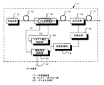
図1は本発明の実施例1に係わる光送信装置を示すブロック図である。図1に示すように、本実施例の光送信装置11は所定の波長のレーザ光を送出する光送出部12と、光送出部12に接続され、レーザ光を伝送する光ファイバ部13と、光ファイバ部13に接続され、データ信号に従ってレーザ光を変調するマッハツェンダ型光変調器14と、光変調器に接続され、変調されたレーザ光を伝送する光ファイバ部15と、光ファイバ部15に接続され、変調されたレーザ光を分岐する光分岐部16と、分岐された一方のレーザ光を更に伝送する光ファイバ部17とで構成されている。
FIG. 1 is a block diagram showing an optical transmission apparatus according to
更に、分岐された他方のレーザ光の平均パワーを検出する光検出部18と、光検出部18の出力信号を入力し、前記入力された信号に所定の演算処理を施してマッハツェンダ型光変調器14のバイアス電圧Vbを制御する信号と駆動電圧の振幅Vppを制御する信号を出力する信号処理部19と、バイアス電圧Vbを制御する信号に基づいてマッハツェンダ型光変調器のバイアス電極に電圧を印加するバイアス電圧制御部20と、駆動電圧の振幅Vppを制御する信号に基づいてマッハツェンダ型光変調器14の駆動電極に電圧を印加する駆動電圧制御部21とで構成されている。
Further, a
信号処理部19は駆動電圧の振幅Vppを制御する信号を駆動電圧制御部21に送出し、次に、バイアス電圧Vbを順次変化さる制御信号をバイアス電圧制御部20に送出しながら光検出部18から出力光の平均パワーを読み取り、読み取った平均パワーの変動量を算出する。
The
次に、駆動電圧の振幅Vppを順次変化させながら平均パワーの変動量が所定値以下になるまで上述した処理を繰り返し、平均パワーの変動量が所定値以下になる駆動電圧の振幅Vppを求めている。 Next, the above-described processing is repeated while sequentially changing the drive voltage amplitude Vpp until the average power fluctuation amount becomes a predetermined value or less to obtain the drive voltage amplitude Vpp at which the average power fluctuation amount becomes a predetermined value or less. Yes.
これにより、自動的に駆動電圧の振幅Vppとマッハツェンダ型光変調器14の半波長電圧Vπとの差が光検出部18の検出限界および信号処理部19の処理精度の範囲内に収められ、駆動電圧の振幅Vppを最適値Vπに設定することが可能である。
As a result, the difference between the amplitude Vpp of the drive voltage and the half-wave voltage Vπ of the Mach-Zehnder type
その後、データ信号入力端子22から入力されるデータ信号に従って設定された振幅Vppを有する駆動電圧を駆動電極に印加することによりレーザ光が変調され、変調された光信号を光ファイバ部17より光通信システム(図示せず)に送出することができる。
Thereafter, the laser light is modulated by applying a drive voltage having an amplitude Vpp set according to the data signal input from the data
以上説明したように、本実施例の光送信装置11によれば、MZ型光変調器14の駆動電圧の振幅Vppをバイアス電圧Vbによらず自動的に最適値Vπに設定できるので、作業時間の短縮と費用の低減を図ることができる。また、何度でも再調整することができる。
As described above, according to the
従って、伝送される光信号の品質を一定に維持することができ、安定して長距離伝送がおこなえる光通信システムを実現することが可能である。 Therefore, the quality of the transmitted optical signal can be maintained constant, and an optical communication system that can stably perform long-distance transmission can be realized.
次に、マッハツェンダ型光変調器14の駆動電圧を最適値Vπに制御する駆動電圧制御装置について説明する。本実施例は、実施例1で示した光送信装置を実現するためのものである。
Next, a drive voltage control device that controls the drive voltage of the Mach-Zehnder
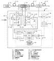
図2は本発明のマッハツェンダ型光変調器の駆動電圧制御装置を示すブロック図である。図2に示すように、駆動電圧制御装置31において、光検出部18は光分岐部16により分岐された一方の光を受光し、その平均パワーに比例する受光電流を出力する受光素子32と、受光素子32の受光電流を受光電圧に変換するI/V変換器33とで構成されている。
FIG. 2 is a block diagram showing a drive voltage control device for a Mach-Zehnder optical modulator according to the present invention. As shown in FIG. 2, in the drive
信号処理部19は受光電圧をデジタル信号に変換するA/D変換器34と、所定の演算処理をおこなうマイクロプロセッサ35と、バイアス電極に印加する電圧を制御する信号をアナログ信号に変換するD/A変換器36と、駆動電極に印加する電圧を制御する信号をアナログ信号に変換するD/A変換器37と、制御プログラムなどを格納する記憶装置38とで構成されている。
The
記憶装置38はマイクロプロセッサ35に接続された半導体メモリ、磁気ディスク、磁気テープ、光ディスクなどのいずれでも構わない。
The
バイアス電圧制御部20はD/A変換器36の出力がバイアス電極に印加する電圧になるように増幅するアンプ39と、アンプ39の出力とMZ型光変調器14のバイアス電圧印加端子40との間に接続され、コイル41とコンデンサ42と終端抵抗43を有するローパスフィルタ44とで構成されている。
The bias
ローパスフィルタ44によりノイズが除去され、バイアス電圧Vbに重畳されたノイズの影響を低減することができる。
Noise is removed by the low-
駆動電圧制御部21はD/A変換器37の出力信号によりデータ入力端子22から入力されるデータ信号が駆動電極に印加する電圧の振幅になるように利得が変えられる可変利得アンプ45と、可変利得アンプ45の出力とMZ型光変調器14の駆動電圧入力端子46との間に接続された、コンデンサ47とコイル48と終端抵抗49を有するハイパスフィルタ50とで構成されている。
The drive
可変利得アンプ45は、利得としてデータ入力端子22から入力されるデータ信号の振幅をMZ型光変調器14の半波長電圧Vπの2倍程度まで増幅できるものが望ましく、例えば、データ信号の振幅が1V程度、半波長電圧Vπが5V程度の場合には最大利得として10倍程度あることが望ましい。また、応答速度としてデータ信号伝送速度以上、例えば600Mbpsから10Gbps程度のデータ伝送速度に対しては1nsから50ps程度以下であることが望ましい。
The
ハイパスフィルタ50によりDC成分が除去され、駆動電圧の振幅Vpp成分のみを駆動電極に印加することができる。
The DC component is removed by the high-
マイクロプロセッサ35は記憶装置38から実行プログラムをロードして、所定の演算処理をおこなう。即ち、駆動電極に印加する電圧の振幅を制御する信号をD/A変換器37に送出し、次に、バイアス電極に印加する電圧を順次変化さる制御信号をD/A変換器36に送出しながらI/V変換器33からの受光電圧をA/D変換器34で読み取り、平均パワーの変動量を算出する。
The
次に、駆動電圧の振幅Vppを順次変化させながら平均パワーの変動量が所定値以下になるまで上記処理を繰り返し、平均パワーの変動量が所定値以下になる駆動電圧の振幅Vppを最適値Vπとしている。 Next, the above processing is repeated while sequentially changing the amplitude Vpp of the drive voltage until the fluctuation amount of the average power becomes a predetermined value or less, and the amplitude Vpp of the drive voltage at which the fluctuation amount of the average power becomes less than the predetermined value is set to the optimum value Vπ. It is said.
これにより、駆動電圧の振幅Vppとマッハツェンダ型光変調器14の半波長電圧Vπとの差が光検出部18の検出限界および信号処理部19の処理精度の範囲内に収められ、駆動電圧の振幅Vppを最適値Vπに設定することが可能である。
As a result, the difference between the amplitude Vpp of the drive voltage and the half-wave voltage Vπ of the Mach-Zehnder
以上説明したように、本実施例のマッハツェンダ型光変調器14の駆動電圧制御装置31によれば、MZ型光変調器14の駆動電圧の振幅Vppをバイアス電圧Vbによらず自動的に最適値Vπに設定できるので、作業時間の短縮と費用の低減を図ることができる。
As described above, according to the drive
また、MZ型光変調器14を光送信装置11に組み込んだ後に何度でも再調整することができる。更に、既設の光送信装置に追加することも容易である。
Further, readjustment can be performed any number of times after the MZ type
従って、伝送される光信号の品質を一定に維持することができ、安定して長距離伝送がおこなえる光送信装置を提供することが可能である。 Therefore, it is possible to provide an optical transmission device that can maintain the quality of the transmitted optical signal constant and can perform long-distance transmission stably.
ここでは、記憶装置38からプログラムをロードして実行する場合について説明したが、マイクロプロセッサ35内のROM領域にファームウェアとして直接格納して実行するようにしても構わない。また、ネットワークを介してプログラムをダウンロードして実行するようにしても構わない。ネットワークによれば再調整や演算処理の条件をリモートコントロールすることができるので、保守管理が容易である。
Although the case where the program is loaded from the
また、マイクロプロセッサ35により所定の演算処理をおこなう場合について説明したが、演算処理の一部または全部を個別の電子回路とロジック回路を組み合わせておこなっても構わない。
Further, although the case where the predetermined arithmetic processing is performed by the
更に、可変利得アンプ44のゲインの設定をD/Aコンバータ37からのアナログ信号でおこなう場合について説明したが、デジタル信号でおこなうようにしても構わない。
Furthermore, although the case where the gain of the
次に、マッハツェンダ型光変調器14の駆動電圧を最適値に制御する駆動電圧制御方法について説明する。本実施例は、実施例2で示した駆動電圧制御装置の機能を実現するためのものである。
Next, a driving voltage control method for controlling the driving voltage of the Mach-Zehnder type
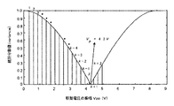
図3は本発明の駆動電圧制御方法を示すフローチャート、図4は任意の駆動電圧を印加した時の光出力波形を示す図、図5は駆動電圧の振幅Vppをパラメータとしてバイアス電圧Vbと光出力の平均パワーの関係を示す図、図6は駆動電圧の振幅Vppと光出力の平均パワーの変動量との関係を示す図である。 3 is a flowchart showing a driving voltage control method according to the present invention, FIG. 4 is a diagram showing a light output waveform when an arbitrary driving voltage is applied, and FIG. 5 is a bias voltage Vb and a light output using the amplitude Vpp of the driving voltage as a parameter. FIG. 6 is a diagram showing a relationship between the amplitude Vpp of the drive voltage and the fluctuation amount of the average power of the optical output.
まず、始めに駆動電圧の振幅Vppを最適値Vπに制御する原理について図4および図5を用いて説明する。 First, the principle of controlling the drive voltage amplitude Vpp to the optimum value Vπ will be described with reference to FIGS. 4 and 5. FIG.
図4に示すように、MZ型光変調器14の特性が最もリニアになる最適なバイアス電圧Vboptはデータ入力端子22に入力される電気信号の各論理値に対応して光出力が最大になる電圧V1と光出力が最小になる電圧V0を用いて、Vbopt=V0+(V1−V0)/2で表され、MZ型光変調器14の最適な駆動電圧の振幅VppはVpp=V1−V0=Vπで表される。
As shown in FIG. 4, the optimum bias voltage Vbopt where the characteristics of the MZ type
これに対して、MZ変調器14の任意の印加電圧をV0x、V1xとすると、バイアス電圧VbはVb=V0x+(V1x−V0x)/2であり、また駆動電圧の振幅VppはVpp=V1x−V0xとなる。
On the other hand, when arbitrary applied voltages of the
MZ変調器14の駆動電圧と光出力の入出力特性は通常三角関数などの周期関数を用いて、
この式(1)より駆動電圧がV1xの時の透過率は、
上記の式(4)、式(5)からMZ型光変調器14の駆動電圧がV0x、V1xの場合、即ち駆動電圧の振幅VppがVpp=V1x−V0xの場合の出力光の平均パワーPavは、
次に、式(6)により駆動電圧の振幅Vppを一定にしてバイアス電圧Vbを順次変化させた時の平均パワーPavの変化を調べると、駆動電圧の振幅Vppが半波長電圧Vπより大きいかまたは小さい場合に平均パワーPavは周期的に変動するが、Vπに等しいときは一定になることがわかる。 Next, when the change in the average power Pav when the bias voltage Vb is sequentially changed with the drive voltage amplitude Vpp being constant according to the equation (6), the drive voltage amplitude Vpp is greater than the half-wave voltage Vπ or It can be seen that the average power Pav varies periodically when it is small, but is constant when it is equal to Vπ.
例えば、図5(a)に示すように、Vπ=4.2V、Vpp=V1x−V0x=0.9Vπとしてバイアス電圧Vbを−8Vから+8Vまで順次変化させると光出力の平均パワーPavは周期2Vπで変動している。 For example, as shown in FIG. 5A, when Vπ = 4.2V, Vpp = V1x−V0x = 0.9Vπ, and the bias voltage Vb is sequentially changed from −8V to + 8V, the average power Pav of the optical output is 2Vπ in a cycle. It is fluctuating.
また、図5(b)に示すように、Vpp=V1x−V0x=Vπの場合はバイアス電圧Vbを−8Vから+8Vまで順次変化させても光出力の平均パワーPavはバイアス電圧Vbによらず一定である。 As shown in FIG. 5B, when Vpp = V1x−V0x = Vπ, the average power Pav of the optical output is constant regardless of the bias voltage Vb even if the bias voltage Vb is changed sequentially from −8V to + 8V. It is.
更に、図5(c)に示すように、Vpp=V1x−V0x=1.1Vπの場合はバイアス電圧Vbを−8Vから+8Vまで順次変化させると再び光出力の平均パワーPavは周期2Vπで変動する。 Further, as shown in FIG. 5C, when Vpp = V1x−V0x = 1.1Vπ, the average power Pav of the light output again fluctuates with a cycle of 2Vπ when the bias voltage Vb is sequentially changed from −8V to + 8V. .
これより、駆動電圧の振幅Vppをパラメータとしてバイアス電圧Vbを順次変化させ、バイアス電圧Vbによらず出力光の平均パワーPavが一定になる駆動電圧の振幅Vppを見出すことにより、駆動電圧の振幅Vppを最適値Vπに設定することが可能である。 Thus, the drive voltage amplitude Vpp is obtained by sequentially changing the bias voltage Vb using the drive voltage amplitude Vpp as a parameter and finding the drive voltage amplitude Vpp at which the average power Pav of the output light is constant regardless of the bias voltage Vb. Can be set to the optimum value Vπ.
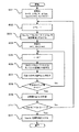
次に、以上の原理に基づく本発明の駆動電圧制御方法を示すフローチャートについて説明する。図3に示すように、始めに初期化をおこないカウンタkをリセットしてバイアス電圧Vbを順次増加させるステップΔVbとステップ数N、駆動電圧の振幅Vppを順次増加させるステップΔVppと初期値Vpp(0)、平均パワーPavの変動量の初期値Var(0)を設定する(ステップS01)。 Next, a flowchart showing a drive voltage control method of the present invention based on the above principle will be described. As shown in FIG. 3, first, initialization is performed, the counter k is reset, the step ΔVb and the number N of steps for sequentially increasing the bias voltage Vb, and the step ΔVpp and the initial value Vpp (0) for sequentially increasing the amplitude Vpp of the drive voltage. ), The initial value Var (0) of the fluctuation amount of the average power Pav is set (step S01).
次に、カウンタkを1つ増やして(ステップS02)、駆動電圧の振幅Vpp(k)を、Vpp(k)=Vpp(k−1)+ΔVppより算出し、D/A変換器37と駆動電圧制御部21を介して駆動電極にVpp(k)を印加する(ステップS03)。
Next, the counter k is incremented by 1 (step S02), the drive voltage amplitude Vpp (k) is calculated from Vpp (k) = Vpp (k-1) + ΔVpp, and the D /
次に、初期化としてカウンタiをリセットしてバイアス電圧Vbの初期値Vb(0)を設定した後(ステップS04)、カウンタiを1つ増やして(ステップS05)、バイアス電圧Vb(i)を、Vb(i)=Vb(i−1)+ΔVbより算出し、D/A変換器36とバイアス電圧制御部20を介してバイアス電極にVb(i)を印加する(ステップS06)。
Next, after initialization, the counter i is reset and the initial value Vb (0) of the bias voltage Vb is set (step S04), the counter i is incremented by one (step S05), and the bias voltage Vb (i) is increased. Vb (i) = Vb (i−1) + ΔVb, and Vb (i) is applied to the bias electrode via the D /
これにより、駆動電圧の振幅がVpp(k)でバイアス電圧がVb(i)の時の出力光の平均パワーPav(i)がA/D変換器34から読込みこまれてマイクロプロセッサ35のRAMに記憶される(ステップS07)。
As a result, the average power Pav (i) of the output light when the drive voltage amplitude is Vpp (k) and the bias voltage is Vb (i) is read from the A /
このループをバイアス電圧Vbのステップ数Nだけ繰り返すため、カウンタiが所定のステップ数Nになったか否かが判定される(ステップS08)。 Since this loop is repeated for the number of steps N of the bias voltage Vb, it is determined whether or not the counter i has reached a predetermined number of steps N (step S08).
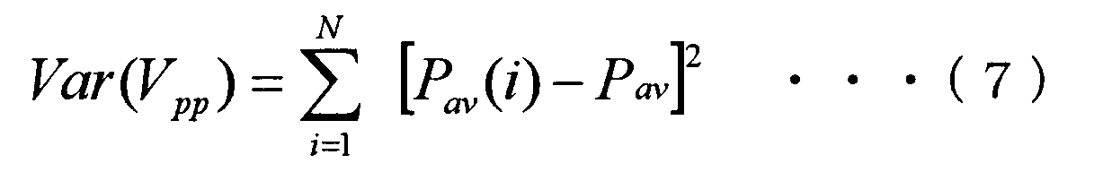
所定のステップ数Nに達していない場合はステップS05に戻り、所定のステップ数Nに達した場合は読込んだN個の平均パワーPavの変動量Var(k)を算出する(ステップS09)。変動量Var(k)は、例えば式(7)に示す統計分散を用いる。この統計分散値は出力光の平均パワーPavの変動が大きい程大きくなる。
駆動電圧の振幅Vppが半波長電圧Vπに一致するところで統計分散値は急峻な極小値(理論値は0)をとり、バイアス電圧Vbによらず出力光の平均パワーPavは一定であることを示している。 When the amplitude Vpp of the drive voltage coincides with the half-wave voltage Vπ, the statistical dispersion value takes a steep minimum value (theoretical value is 0), indicating that the average power Pav of the output light is constant regardless of the bias voltage Vb. ing.
駆動電圧の振幅Vppが増加するに従い統計分散値は再び増加していく、これは駆動電圧の振幅Vppが半波長電圧Vπより遠ざかっていくので出力光の平均パワーPavの変動が大きくなったことを示している。 As the drive voltage amplitude Vpp increases, the statistical dispersion value increases again. This is because the drive voltage amplitude Vpp moves away from the half-wave voltage Vπ, so that the fluctuation of the average power Pav of the output light increases. Show.
更に、駆動電圧の振幅Vppが増加すると再び半波長電圧Vπに近づいていくので統計分散値は周期2Vπで振動することが分かる。 Furthermore, it can be seen that as the amplitude Vpp of the drive voltage increases, it approaches the half-wave voltage Vπ again, so that the statistical dispersion value oscillates with a period of 2Vπ.
次に、この変動量Var(k)が所定の値以下か否かの判定は、駆動電圧の振幅Vppが半波長電圧Vπに一致するところで統計分散値は急峻な極小値を持つことを利用して変動量Var(k)が一つ前の変動量Var(k−1)より大きいか否かによりおこなわれる(ステップS10)。 Next, the determination of whether or not the fluctuation amount Var (k) is equal to or less than a predetermined value is based on the fact that the statistical dispersion value has a steep minimum value where the amplitude Vpp of the drive voltage matches the half-wave voltage Vπ. This is performed depending on whether or not the variation amount Var (k) is larger than the previous variation amount Var (k−1) (step S10).
この変動量Var(k)が所定の値以上の場合は駆動電圧の振幅Vppがまだ最適値Vπに達していないのでステップS02に戻り、カウンタkを1つ増やしてステップS03からステップS09を再度実行する。 If the fluctuation amount Var (k) is equal to or greater than a predetermined value, the amplitude Vpp of the drive voltage has not yet reached the optimum value Vπ, so the process returns to step S02, the counter k is incremented by 1, and steps S03 to S09 are executed again. To do.
一方、所定の値以下の場合は駆動電圧の振幅Vppが最適値Vπに達したので、その時点で駆動電極に印加している電圧Vpp(k)を駆動電圧の振幅Vppの最適値Vπとしている(ステップS11)。 On the other hand, if it is equal to or smaller than the predetermined value, the drive voltage amplitude Vpp has reached the optimum value Vπ, and the voltage Vpp (k) applied to the drive electrode at that time is set as the optimum value Vπ of the drive voltage amplitude Vpp. (Step S11).
以上説明したように、本発明の駆動電圧制御方法によれば、MZ型光変調器14の駆動電圧の振幅Vppをバイアス電圧Vbによらず自動的に最適値Vπに設定できるので、作業時間の短縮と費用の低減を図ることができる。また、MZ型光変調器を装置に組み込んだ後でも制御方法を実行するプログラムを再度起動することにより、何度でも再調整することができる。
As described above, according to the driving voltage control method of the present invention, the amplitude Vpp of the driving voltage of the MZ type
従って、伝送される光信号の品質を一定に維持することができ、安定して長距離伝送がおこなえる光通信システムを実現することが可能である。 Therefore, the quality of the transmitted optical signal can be maintained constant, and an optical communication system that can stably perform long-distance transmission can be realized.
また、本発明の駆動電圧制御プログラムでは、駆動電圧を制御するアルゴリズムを半導体メモリ、磁気ディスク、磁気テープ、光ディスクなどの記憶媒体に記憶しコンピュータで利用することができる。 In the drive voltage control program of the present invention, an algorithm for controlling the drive voltage can be stored in a storage medium such as a semiconductor memory, a magnetic disk, a magnetic tape, or an optical disk and used by a computer.
11 光送信装置
12 光送出部
13、15、17 光ファイバ部
14 MZ型光変調器
16 光分岐部
18 光検出部
19 信号処理部
20 バイアス電圧制御部
21 駆動電圧制御部
22 データ入力端子
31 駆動電圧制御装置
32 受光素子
33 I/V変換器
34 A/D変換器
35 マイクロプロセッサ
36、37 D/A変換器
38 記憶装置
39 アンプ
40 バイアス電圧入力端子
41、48 コイル
42、47 コンデンサ
43、49 抵抗
44 ローパスフィルタ
45 可変利得アンプ
46 駆動電圧入力端子
50 ハイパスフィルタ
DESCRIPTION OF
Claims (6)
前記光送出部に接続され、前記レーザ光を伝送する光ファイバ部と、
前記光ファイバ部に接続され、データ信号に従って前記レーザ光を変調するマッハツェンダ型光変調器と、
前記光変調器に接続され、前記変調されたレーザ光を伝送する光ファイバ部と、
前記光ファイバ部に接続され、前記変調されたレーザ光を分岐する光分岐部と、
前記分岐された一方のレーザ光を更に伝送する光ファイバ部と、
前記分岐された他方のレーザ光の平均パワーを検出する光検出部と、
前記光検出部の出力信号を入力し、前記入力された信号に所定の演算処理を施して前記マッハツェンダ型光変調器のバイアス電圧を制御する信号と駆動電圧を制御する信号を出力する信号処理部と、
前記バイアス電圧を制御する信号に基づいて前記マッハツェンダ型光変調器のバイアス電極に電圧を印加するバイアス電圧制御部と、
前記駆動電圧を制御する信号に基づいて前記マッハツェンダ型光変調器の駆動電極に電圧を印加する駆動電圧制御部と、
を具備し、
前記バイアス電圧を順次変化させたときの前記平均パワーの変動量が所定値以下になる前記駆動電圧を求めた後、前記駆動電圧をデータ信号に従ってマッハツェンダ型光変調器に印加することにより前記レーザ光を変調し、この変調されたレーザ光を送出するようにしたことを特徴とする光送信装置。 A light sending unit for sending laser light of a predetermined wavelength;
An optical fiber part connected to the light sending part and transmitting the laser light;
A Mach-Zehnder optical modulator that is connected to the optical fiber unit and modulates the laser light in accordance with a data signal;
An optical fiber unit connected to the optical modulator and transmitting the modulated laser beam;
An optical branching unit connected to the optical fiber unit and branching the modulated laser beam;
An optical fiber part for further transmitting the branched one laser beam;
A light detection unit for detecting an average power of the other branched laser beam;
A signal processing unit that receives an output signal of the light detection unit, performs a predetermined arithmetic processing on the input signal, and outputs a signal for controlling a bias voltage of the Mach-Zehnder optical modulator and a signal for controlling a driving voltage When,
A bias voltage control unit for applying a voltage to a bias electrode of the Mach-Zehnder optical modulator based on a signal for controlling the bias voltage;
A drive voltage control unit for applying a voltage to the drive electrode of the Mach-Zehnder optical modulator based on a signal for controlling the drive voltage;
Comprising
The laser beam is obtained by obtaining the drive voltage at which the fluctuation amount of the average power when the bias voltage is sequentially changed is less than or equal to a predetermined value, and then applying the drive voltage to the Mach-Zehnder type optical modulator according to a data signal. An optical transmitter characterized in that the modulated laser beam is transmitted.
前記マッハツェンダ型光変調器の駆動電極に印加する電圧を設定する電圧発生部と、
前記に設定された電圧を前記駆動電極に印加する駆動電圧制御部と、
前記マッハツェンダ型光変調器のバイアス電極に印加する電圧の振幅を設定する電圧発生部と、
前記設定された電圧を前記バイアス電極に印加するバイアス電圧制御部と、
前記マッハツェンダ型光変調器の出力光の平均パワーを検出する光検出部と、
前記検出した平均パワーに基づいて所定の演算処理をおこなう演算部と、
を具備し、
前記バイアス電極に印加する電圧を順次変化させたときの前記平均パワーの変動量が所定値以下になる前記駆動電極に印加する電圧を求めた後、この電圧を前記データ信号に従って前記駆動電極に印加するようにしたことを特徴とするマッハツェンダ型光変調器の駆動電圧制御装置。 An apparatus for controlling the drive voltage of a Mach-Zehnder optical modulator,
A voltage generator for setting a voltage to be applied to the drive electrode of the Mach-Zehnder optical modulator;
A drive voltage controller that applies the voltage set to the drive electrode;
A voltage generator for setting an amplitude of a voltage applied to the bias electrode of the Mach-Zehnder optical modulator;
A bias voltage controller for applying the set voltage to the bias electrode;
A light detection unit for detecting an average power of the output light of the Mach-Zehnder optical modulator;
A calculation unit that performs a predetermined calculation process based on the detected average power;
Comprising
After obtaining a voltage to be applied to the drive electrode that causes the fluctuation amount of the average power when the voltage applied to the bias electrode is sequentially changed to a predetermined value or less, this voltage is applied to the drive electrode in accordance with the data signal. A drive voltage control device for a Mach-Zehnder type optical modulator, characterized in that:
前記電圧を設定する処理および前記所定の演算処理をおこなうマイクロプロセッサと、
前記バイアス電極に印加する電圧を制御する信号を出力するD/A変換器と、
前記駆動電極に印加する電圧を制御する信号を出力するD/A変換器と、
を有することを特徴とする請求項2記載のマッハツェンダ型光変調器の駆動電圧制御装置。 An A / D converter for inputting the average power;
A microprocessor for performing the process of setting the voltage and the predetermined calculation process;
A D / A converter that outputs a signal for controlling a voltage applied to the bias electrode;
A D / A converter that outputs a signal for controlling a voltage applied to the drive electrode;
The drive voltage control device for a Mach-Zehnder type optical modulator according to claim 2, wherein:
前記可変利得アンプの出力と前記駆動電極との間に接続され、前記駆動電圧の高い周波数の振幅のみを通過させるフィルタと、
を有することを特徴とする請求項2記載のマッハツェンダ型光変調器の駆動電圧制御装置。 A variable gain amplifier in which the drive voltage controller can vary the gain by a control signal of the voltage generator;
A filter connected between the output of the variable gain amplifier and the drive electrode and passing only the high frequency amplitude of the drive voltage;
The drive voltage control device for a Mach-Zehnder type optical modulator according to claim 2, wherein:
前記マッハツェンダ型光変調器の駆動電極に印加する電圧を設定する工程と、
前記設定された電圧を前記駆動電極に印加する工程と、
前記マッハツェンダ型光変調器のバイアス電極に印加する電圧を設定する工程と、
前記設定された電圧を前記バイアス電極に印加する工程と、
前記バイアス電極に印加する電圧を順次変化させながら前記マッハツェンダ型光変調器の出力光の平均パワーを読み取る工程と、
前記読み取った平均パワーの変動量を求める工程と、
前記駆動電極に印加する電圧を順次変化させながら前記変動量が所定値以下に達したか否かを判定する工程と、
前記変動量が所定値以下に達した場合に、前記駆動電極に印加されている電圧を前記マッハツェンダ型光変調器の駆動電圧とする工程と、
を有することを特徴とするマッハツェンダ型光変調器の駆動電圧制御方法。 A method for controlling a drive voltage of a Mach-Zehnder optical modulator,
Setting a voltage to be applied to the drive electrode of the Mach-Zehnder optical modulator;
Applying the set voltage to the drive electrode;
Setting a voltage to be applied to the bias electrode of the Mach-Zehnder optical modulator;
Applying the set voltage to the bias electrode;
Reading the average power of the output light of the Mach-Zehnder optical modulator while sequentially changing the voltage applied to the bias electrode;
Obtaining the read average power fluctuation amount;
Determining whether the variation amount has reached a predetermined value or less while sequentially changing the voltage applied to the drive electrode;
A step of setting a voltage applied to the drive electrode as a drive voltage of the Mach-Zehnder optical modulator when the fluctuation amount reaches a predetermined value or less;
A drive voltage control method for a Mach-Zehnder type optical modulator.
前記マッハツェンダ型光変調器の駆動電極に印加する電圧を設定する機能と、
前記設定された電圧を前記駆動電極に印加する制御信号を出力する機能と、
前記マッハツェンダ型光変調器のバイアス電極に印加する電圧を設定する機能と、
前記設定された電圧を前記バイアス電極に印加する制御信号を出力する機能と、
前記マッハツェンダ型光変調器の出力光の平均パワーを入力する機能と、
前記バイアス電極に印加する電圧を順次変化させながら前記出力光の平均パワーを読み取り、前記読み取った平均パワーの変動量を求める機能と、
前記駆動電極に印加する電圧を順次変化させながら前記変動量が所定値以下に達したか否かを判定する機能と、
前記変動量が所定値以下に達した場合に、前記駆動電極に印加されている電圧を前記マッハツェンダ型光変調器の駆動電圧とする機能と、
を有することを特徴とするコンピュータで利用されるプログラム。 A program for controlling the drive voltage of a Mach-Zehnder optical modulator,
A function of setting a voltage to be applied to the drive electrode of the Mach-Zehnder optical modulator;
A function of outputting a control signal for applying the set voltage to the drive electrode;
A function of setting a voltage to be applied to the bias electrode of the Mach-Zehnder optical modulator;
A function of outputting a control signal for applying the set voltage to the bias electrode;
A function of inputting the average power of the output light of the Mach-Zehnder optical modulator;
A function of reading the average power of the output light while sequentially changing the voltage applied to the bias electrode, and obtaining a fluctuation amount of the read average power;
A function of determining whether or not the variation amount has reached a predetermined value or less while sequentially changing the voltage applied to the drive electrode;
A function of setting a voltage applied to the drive electrode as a drive voltage of the Mach-Zehnder optical modulator when the variation amount reaches a predetermined value or less;
A program used in a computer, characterized by comprising:
Priority Applications (1)
| Application Number | Priority Date | Filing Date | Title |
|---|---|---|---|
| JP2003324079A JP2005091663A (en) | 2003-09-17 | 2003-09-17 | Drive voltage control method, drive voltage control program, drive voltage control device, and optical transmitter for Mach-Zehnder type optical modulator |
Applications Claiming Priority (1)
| Application Number | Priority Date | Filing Date | Title |
|---|---|---|---|
| JP2003324079A JP2005091663A (en) | 2003-09-17 | 2003-09-17 | Drive voltage control method, drive voltage control program, drive voltage control device, and optical transmitter for Mach-Zehnder type optical modulator |
Publications (1)
| Publication Number | Publication Date |
|---|---|
| JP2005091663A true JP2005091663A (en) | 2005-04-07 |
Family
ID=34454935
Family Applications (1)
| Application Number | Title | Priority Date | Filing Date |
|---|---|---|---|
| JP2003324079A Pending JP2005091663A (en) | 2003-09-17 | 2003-09-17 | Drive voltage control method, drive voltage control program, drive voltage control device, and optical transmitter for Mach-Zehnder type optical modulator |
Country Status (1)
| Country | Link |
|---|---|
| JP (1) | JP2005091663A (en) |
Cited By (7)
| Publication number | Priority date | Publication date | Assignee | Title |
|---|---|---|---|---|
| JP2007094127A (en) * | 2005-09-29 | 2007-04-12 | Yokogawa Electric Corp | Optical modulator and optical modulator control method |
| JP2008033292A (en) * | 2006-07-03 | 2008-02-14 | Matsushita Electric Ind Co Ltd | Optical transmission equipment |
| JP2008092172A (en) * | 2006-09-29 | 2008-04-17 | Fujitsu Ltd | Optical transmitter |
| JP2010127777A (en) * | 2008-11-27 | 2010-06-10 | Sumitomo Osaka Cement Co Ltd | Electric field measuring device |
| WO2017208803A1 (en) * | 2016-06-02 | 2017-12-07 | 三菱電機株式会社 | Optical modulation device and method for controlling optical modulation device |
| WO2023144868A1 (en) * | 2022-01-25 | 2023-08-03 | 日本電信電話株式会社 | Optical pulse generation device and generation method |
| JP7817598B2 (en) | 2022-01-25 | 2026-02-19 | Ntt株式会社 | Optical pulse generating device and generating method |
-
2003
- 2003-09-17 JP JP2003324079A patent/JP2005091663A/en active Pending
Cited By (11)
| Publication number | Priority date | Publication date | Assignee | Title |
|---|---|---|---|---|
| JP2007094127A (en) * | 2005-09-29 | 2007-04-12 | Yokogawa Electric Corp | Optical modulator and optical modulator control method |
| JP2008033292A (en) * | 2006-07-03 | 2008-02-14 | Matsushita Electric Ind Co Ltd | Optical transmission equipment |
| JP2008092172A (en) * | 2006-09-29 | 2008-04-17 | Fujitsu Ltd | Optical transmitter |
| US8145069B2 (en) | 2006-09-29 | 2012-03-27 | Fujitsu Limited | Optical transmitter |
| JP2010127777A (en) * | 2008-11-27 | 2010-06-10 | Sumitomo Osaka Cement Co Ltd | Electric field measuring device |
| EP2378298A4 (en) * | 2008-11-27 | 2015-10-28 | Sumitomo Osaka Cement Co Ltd | Electric field measuring device |
| WO2017208803A1 (en) * | 2016-06-02 | 2017-12-07 | 三菱電機株式会社 | Optical modulation device and method for controlling optical modulation device |
| JP6271106B1 (en) * | 2016-06-02 | 2018-01-31 | 三菱電機株式会社 | Light modulation device and method for controlling light modulation device |
| WO2023144868A1 (en) * | 2022-01-25 | 2023-08-03 | 日本電信電話株式会社 | Optical pulse generation device and generation method |
| JPWO2023144868A1 (en) * | 2022-01-25 | 2023-08-03 | ||
| JP7817598B2 (en) | 2022-01-25 | 2026-02-19 | Ntt株式会社 | Optical pulse generating device and generating method |
Similar Documents
| Publication | Publication Date | Title |
|---|---|---|
| US7308210B2 (en) | Optical modulating device, optical transmitting apparatus using the same, method of controlling optical modulating device, and control program recording medium | |
| US7555226B2 (en) | Automatic bias control for an optical modulator | |
| EP2227715B1 (en) | Bias controller | |
| JP3405046B2 (en) | Laser light generator | |
| KR100450745B1 (en) | Apparatus and method for controlling electro-optic modulator | |
| EP1884820A2 (en) | Control system and control method for controlling optical modulator | |
| CN103248432A (en) | Optical transmitter and method for controlling bias for optical modulator | |
| US7215894B2 (en) | Optical transmitter device | |
| KR100606100B1 (en) | Optical modulator with bias control device and bias control method using same | |
| US11381316B2 (en) | Optical transmitter and optical transmission method | |
| US8000612B2 (en) | Optical transmission device | |
| US10890822B2 (en) | Mach-zehnder optical modulator | |
| JP2005091663A (en) | Drive voltage control method, drive voltage control program, drive voltage control device, and optical transmitter for Mach-Zehnder type optical modulator | |
| JP2020134883A (en) | Optical transmitter and control method for optical transmitter | |
| JP3822548B2 (en) | Optical modulator controller | |
| US7630651B2 (en) | Method and apparatus for controlling bias point of optical transmitter | |
| JP3749874B2 (en) | OPTICAL MODULATOR CONTROL DEVICE, OPTICAL TRANSMITTER USING SAME, OPTICAL MODULATOR CONTROL METHOD, AND CONTROL PROGRAM RECORDING MEDIUM | |
| CN114280768B (en) | Device and method for optical signal processing | |
| JP4008793B2 (en) | Optical modulator driving device and optical transmission device using the same | |
| JP2001244896A (en) | Optical transmitter | |
| CN115396035B (en) | Dispersion precompensation method, device, electronic equipment and storage medium | |
| JP2017125867A (en) | Light transmitter, and source voltage control method | |
| JP7347532B2 (en) | LiDAR device, LiDAR system, and measurement method using LiDAR | |
| WO2023233528A1 (en) | Short optical pulse generation device, short optical pulse generation method, and program | |
| CN121142855A (en) | Bias voltage control method for pilot-free MZ modulator |
Legal Events
| Date | Code | Title | Description |
|---|---|---|---|
| RD02 | Notification of acceptance of power of attorney |
Free format text: JAPANESE INTERMEDIATE CODE: A7422 Effective date: 20050415 |
|
| RD04 | Notification of resignation of power of attorney |
Free format text: JAPANESE INTERMEDIATE CODE: A7424 Effective date: 20050606 |