JP2005079110A - Semiconductor device and manufacturing method thereof - Google Patents
Semiconductor device and manufacturing method thereof Download PDFInfo
- Publication number
- JP2005079110A JP2005079110A JP2003209618A JP2003209618A JP2005079110A JP 2005079110 A JP2005079110 A JP 2005079110A JP 2003209618 A JP2003209618 A JP 2003209618A JP 2003209618 A JP2003209618 A JP 2003209618A JP 2005079110 A JP2005079110 A JP 2005079110A
- Authority
- JP
- Japan
- Prior art keywords
- impurity
- semiconductor substrate
- implanted
- semiconductor device
- heat treatment
- Prior art date
- Legal status (The legal status is an assumption and is not a legal conclusion. Google has not performed a legal analysis and makes no representation as to the accuracy of the status listed.)
- Pending
Links
Images

Classifications
-
- H—ELECTRICITY
- H10—SEMICONDUCTOR DEVICES; ELECTRIC SOLID-STATE DEVICES NOT OTHERWISE PROVIDED FOR
- H10P—GENERIC PROCESSES OR APPARATUS FOR THE MANUFACTURE OR TREATMENT OF DEVICES COVERED BY CLASS H10
- H10P30/00—Ion implantation into wafers, substrates or parts of devices
- H10P30/20—Ion implantation into wafers, substrates or parts of devices into semiconductor materials, e.g. for doping
- H10P30/202—Ion implantation into wafers, substrates or parts of devices into semiconductor materials, e.g. for doping characterised by the semiconductor materials
- H10P30/204—Ion implantation into wafers, substrates or parts of devices into semiconductor materials, e.g. for doping characterised by the semiconductor materials into Group IV semiconductors
-
- H—ELECTRICITY
- H10—SEMICONDUCTOR DEVICES; ELECTRIC SOLID-STATE DEVICES NOT OTHERWISE PROVIDED FOR
- H10D—INORGANIC ELECTRIC SEMICONDUCTOR DEVICES
- H10D84/00—Integrated devices formed in or on semiconductor substrates that comprise only semiconducting layers, e.g. on Si wafers or on GaAs-on-Si wafers
- H10D84/01—Manufacture or treatment
- H10D84/0123—Integrating together multiple components covered by H10D12/00 or H10D30/00, e.g. integrating multiple IGBTs
- H10D84/0126—Integrating together multiple components covered by H10D12/00 or H10D30/00, e.g. integrating multiple IGBTs the components including insulated gates, e.g. IGFETs
- H10D84/0165—Integrating together multiple components covered by H10D12/00 or H10D30/00, e.g. integrating multiple IGBTs the components including insulated gates, e.g. IGFETs the components including complementary IGFETs, e.g. CMOS devices
- H10D84/017—Manufacturing their source or drain regions, e.g. silicided source or drain regions
-
- H—ELECTRICITY
- H10—SEMICONDUCTOR DEVICES; ELECTRIC SOLID-STATE DEVICES NOT OTHERWISE PROVIDED FOR
- H10D—INORGANIC ELECTRIC SEMICONDUCTOR DEVICES
- H10D84/00—Integrated devices formed in or on semiconductor substrates that comprise only semiconducting layers, e.g. on Si wafers or on GaAs-on-Si wafers
- H10D84/01—Manufacture or treatment
- H10D84/02—Manufacture or treatment characterised by using material-based technologies
- H10D84/03—Manufacture or treatment characterised by using material-based technologies using Group IV technology, e.g. silicon technology or silicon-carbide [SiC] technology
- H10D84/038—Manufacture or treatment characterised by using material-based technologies using Group IV technology, e.g. silicon technology or silicon-carbide [SiC] technology using silicon technology, e.g. SiGe
-
- H—ELECTRICITY
- H10—SEMICONDUCTOR DEVICES; ELECTRIC SOLID-STATE DEVICES NOT OTHERWISE PROVIDED FOR
- H10P—GENERIC PROCESSES OR APPARATUS FOR THE MANUFACTURE OR TREATMENT OF DEVICES COVERED BY CLASS H10
- H10P30/00—Ion implantation into wafers, substrates or parts of devices
- H10P30/20—Ion implantation into wafers, substrates or parts of devices into semiconductor materials, e.g. for doping
- H10P30/208—Ion implantation into wafers, substrates or parts of devices into semiconductor materials, e.g. for doping of electrically inactive species
-
- H—ELECTRICITY
- H10—SEMICONDUCTOR DEVICES; ELECTRIC SOLID-STATE DEVICES NOT OTHERWISE PROVIDED FOR
- H10P—GENERIC PROCESSES OR APPARATUS FOR THE MANUFACTURE OR TREATMENT OF DEVICES COVERED BY CLASS H10
- H10P30/00—Ion implantation into wafers, substrates or parts of devices
- H10P30/20—Ion implantation into wafers, substrates or parts of devices into semiconductor materials, e.g. for doping
- H10P30/21—Ion implantation into wafers, substrates or parts of devices into semiconductor materials, e.g. for doping of electrically active species
-
- H—ELECTRICITY
- H10—SEMICONDUCTOR DEVICES; ELECTRIC SOLID-STATE DEVICES NOT OTHERWISE PROVIDED FOR
- H10P—GENERIC PROCESSES OR APPARATUS FOR THE MANUFACTURE OR TREATMENT OF DEVICES COVERED BY CLASS H10
- H10P30/00—Ion implantation into wafers, substrates or parts of devices
- H10P30/20—Ion implantation into wafers, substrates or parts of devices into semiconductor materials, e.g. for doping
- H10P30/28—Ion implantation into wafers, substrates or parts of devices into semiconductor materials, e.g. for doping characterised by an annealing step, e.g. for activation of dopants
-
- H—ELECTRICITY
- H10—SEMICONDUCTOR DEVICES; ELECTRIC SOLID-STATE DEVICES NOT OTHERWISE PROVIDED FOR
- H10P—GENERIC PROCESSES OR APPARATUS FOR THE MANUFACTURE OR TREATMENT OF DEVICES COVERED BY CLASS H10
- H10P34/00—Irradiation with electromagnetic or particle radiation of wafers, substrates or parts of devices
- H10P34/40—Irradiation with electromagnetic or particle radiation of wafers, substrates or parts of devices with high-energy radiation
- H10P34/42—Irradiation with electromagnetic or particle radiation of wafers, substrates or parts of devices with high-energy radiation with electromagnetic radiation, e.g. laser annealing
- H10P34/422—Irradiation with electromagnetic or particle radiation of wafers, substrates or parts of devices with high-energy radiation with electromagnetic radiation, e.g. laser annealing using incoherent radiation
-
- H—ELECTRICITY
- H10—SEMICONDUCTOR DEVICES; ELECTRIC SOLID-STATE DEVICES NOT OTHERWISE PROVIDED FOR
- H10P—GENERIC PROCESSES OR APPARATUS FOR THE MANUFACTURE OR TREATMENT OF DEVICES COVERED BY CLASS H10
- H10P95/00—Generic processes or apparatus for manufacture or treatments not covered by the other groups of this subclass
- H10P95/90—Thermal treatments, e.g. annealing or sintering
-
- H—ELECTRICITY
- H10—SEMICONDUCTOR DEVICES; ELECTRIC SOLID-STATE DEVICES NOT OTHERWISE PROVIDED FOR
- H10D—INORGANIC ELECTRIC SEMICONDUCTOR DEVICES
- H10D64/00—Electrodes of devices having potential barriers
- H10D64/01—Manufacture or treatment
- H10D64/021—Manufacture or treatment using multiple gate spacer layers, e.g. bilayered sidewall spacers
Landscapes
- Insulated Gate Type Field-Effect Transistor (AREA)
- Metal-Oxide And Bipolar Metal-Oxide Semiconductor Integrated Circuits (AREA)
Abstract
【課題】加熱処理に用いられる光の吸収効率の向上および均一化が図られて、加熱むらや熱応力の発生を抑制された半導体基板を具備してなり、品質、信頼性、および歩留まりが向上された半導体装置を提供する。
【解決手段】半導体基板1の表層部に、電気的に不活性な第1の不純物を全面的に注入した後、キセノンフラッシュランプによる加熱処理を施す。
【選択図】 図1An object of the present invention is to improve the efficiency and uniformity of absorption of light used for heat treatment, and to provide a semiconductor substrate that suppresses generation of uneven heating and thermal stress, thereby improving quality, reliability, and yield. Provided is a semiconductor device.
An electrically inactive first impurity is entirely injected into a surface layer portion of a semiconductor substrate, and then heat treatment is performed using a xenon flash lamp.
[Selection] Figure 1
Description
【0001】
【発明の属する技術分野】
本発明は、加熱処理が施される半導体基板を具備する半導体装置およびその製造方法に係り、特に加熱処理によって表層部に不純物の拡散領域等が形成される半導体基板を具備する半導体装置およびその製造方法に関する。
【0002】
【従来の技術】
LSIの性能向上は、その集積度を高めること、すなわち半導体を構成する素子の微細化を図ることにより実現できる。近年、集積回路は益々大規模化しており、これに伴って素子の微細化もさらに勢いを増して進んでいる。そして、素子寸法が縮小化されるのに伴い、浅いpn接合の形成はその重要性を増している。
【0003】
浅い不純物拡散領域を形成する方法としては、例えばシリコン(Si)基板中に所定のイオンを低加速エネルギーで注入した後、Si基板に最適化されたアニール処理を施す方法が一般的である(例えば特許文献1〜6参照)。しかしながら、イオン注入で一般に使用されているp型ドーパントであるボロン(B)、あるいはn型ドーパントであるリン(P)や砒素(As)は、Si基板中の拡散係数が大きい。このため、不純物を活性化させるための加熱処理に、たとえアニールに要する時間が短くて済む、ハロゲンランプを用いる急速熱アニール(Rapid Thermal Anneal:RTA)処理を採用しても、不純物がSi基板中の内方および外方に拡散してしまう。このため、イオン注入された不純物において所望の分布プロファイルを得ることが困難である。また、不純物拡散を抑制するためにアニール温度を下げると、不純物の活性化率が大きく低下する問題が起きる。このように、一般のRTA処理では、例えば接合深さが20nm以下の浅い低抵抗拡散層を形成することは困難である。
【0004】
そこで近年、これらの課題を解決するために、不純物の活性化に必要なエネルギーを瞬時に供給する手法として、レーザーアニールおよびフラッシュランプアニールが検討されている。しかしながら、レーザー光線は指向性が良いため、干渉が起こり易く、かつ、照射エリアも限定される。このため、大面積を有するウェーハ(基板)に対する照射エネルギーの均一性および再現性を保つことが難しい。また、レーザー光線は強度の調整が難しく、アニールに適する強度を得難い。このため、単位時間あるいは単位面積当たりのエネルギー密度が高くなり過ぎて、半導体基板表面を溶かしてしまうおそれがある。このように、一般のレーザーアニール法では、不純物活性化処理後の半導体基板表面のモフォロジーが劣化するおそれが指摘されている。
【0005】
他方、最近注目されているフラッシュランプアニール法では、熱源であるXeフラッシュランプの発光が、数100μmsec〜数msecの極めて短い時間内で完了する。これにより、半導体層に注入された不純物イオンの分布を殆ど変化させることなく、不純物イオンを活性化させることが可能である。また、大面積を有する半導体基板全面に対して加熱処理を一括して施すことができ、スループットが高い。しかしながら、フラッシュランプアニール法では、広い照射面積および高速昇降温可能という特徴が、半導体基板に大きな熱応力を生じさせることが懸念される。特に、poly−Si、SiO2、SiN等の複数種類の膜によって表面上にパターンが構成されたウェーハの場合には、各膜種間で加熱むらが発生し易い。このような加熱むらが発生すると、転位や欠陥等の損傷がウェーハに生じ易い。これにより、生産歩留まりが低下し易い。このような場合、基板予備加熱温度あるいはフラッシュランプの照射エネルギーを下げることにより、基板への損傷を回避することはできるが、不純物の十分な活性化は期待できなくなる。このように、一般のフラッシュランプアニール法では、半導体素子の製造過程におけるプロセスウィンドウ(プロセスマージン)が狭いことが問題となっている。
【0006】
【特許文献1】
特開2002−141298号公報
【0007】
【特許文献2】
特開2002−246328号公報
【0008】
【特許文献3】
特開2002−198322号公報
【0009】
【特許文献4】
特開2002−175772号公報
【0010】
【特許文献5】
特開平10−26772号公報
【0011】
【特許文献6】
USP6,417,515号公報
【0012】
【発明が解決しようとする課題】
前述したように、基板の表層部に不純物拡散層を形成する場合、加熱処理の方法に拘らず基板に様々な問題が生じるおそれがある。特に、熱応力による変形や損傷が基板に生じたり、加熱むらによる品質劣化が基板等に生じたりする問題は、基板に不純物拡散層を形成する場合に限らず、基板に加熱処理を施す際にいつでも起こり得る。
【0013】
本発明は、以上説明したような課題を解決するためになされたものであり、その目的とするところは、電気的特性が殆ど劣化されること無く、加熱処理に用いられる光の吸収効率の向上および均一化が図られ、加熱むらや熱応力の発生を抑制されて光による加熱処理が施された半導体基板を具備し、品質、信頼性、および歩留まりが向上された半導体装置を提供することにある。また、電気的特性が殆ど劣化されること無く、加熱処理に用いられる光の吸収効率の向上および均一化が図られて加熱むらや熱応力の発生を抑制された半導体基板に、光による加熱処理により良質なソース・ドレイン拡散層が形成されて、品質および信頼性が向上されたトランジスタを具備するとともに、歩留まりが向上された半導体装置を提供することにある。それとともに、それらのような半導体装置を効率良く容易に製造できる半導体装置の製造方法を提供することにある。
【0014】
【課題を解決するための手段】
前記課題を解決するために、本発明の一態様に係る半導体装置の製造方法は、半導体基板の一主面に電気的に不活性な第1の不純物を全面的に注入する工程と、前記第1の不純物が注入された前記半導体基板に光による加熱処理を施す工程と、を含むことを特徴とするものである。
【0015】
この半導体装置の製造方法においては、半導体基板に光による加熱処理を施すのに先立って、電気的に不活性な第1の不純物を半導体基板に全面的に注入する。すなわち、半導体基板に光による加熱処理を施すのに先立って、半導体基板等の導電型および導電率に影響を及ぼすおそれが殆ど無い第1の不純物を、半導体基板に全面的に注入する。これにより、半導体基板等の電気的特性を殆ど劣化させること無く、半導体基板の光の吸収係数や屈折率を全面的に略均一化した状態で、半導体基板に光による加熱処理を施すことができる。すなわち、半導体基板等の電気的特性を殆ど劣化させること無く、加熱効率の差を殆ど無くして、加熱むらや局所的な加熱による熱応力の発生を抑制した状態で半導体基板に光による加熱処理を施すことができる。また、半導体基板に第1の不純物を注入することによって半導体基板をアモルファス化させ、光の吸収効率(吸収量)を増大させることができる。これにより、加熱処理に必要な光の照射エネルギーを低減させ、半導体基板内に発生する熱応力を抑制して光による加熱処理を施すことができる。
【0016】
このように、本発明の一態様に係る半導体装置の製造方法は、半導体基板等の電気的特性を殆ど劣化させること無く、かつ、半導体基板に熱応力による変形や損傷が生じたり、加熱むらなどによる品質劣化が生じたりするおそれを殆ど無くして、光による加熱処理を半導体基板に効率良く容易に施すことができる。
【0017】
また、前記課題を解決するために、本発明の他の態様に係る半導体装置の製造方法は、半導体基板の一主面上にゲート絶縁膜を有するゲート電極を設ける工程と、前記ゲート電極が設けられた前記半導体基板の一主面に電気的に不活性な第1の不純物を全面的に注入するとともに、前記ゲート電極をマスクとして、前記半導体基板の前記ゲート電極に隣接する領域に、所定の導電型を有する電気的に活性な第2の不純物を注入する工程と、前記第1の不純物および前記第2の不純物が注入された前記半導体基板に光による加熱処理を施すことにより前記第2の不純物を活性化させて、前記所定の導電型を有する浅いソース・ドレイン拡散層を形成する工程と、前記ゲート電極の周囲にゲート側壁膜を設ける工程と、前記ゲート側壁膜が設けられた前記半導体基板の一主面に前記第1の不純物を全面的に注入するとともに、前記ゲート電極および前記ゲート側壁膜をマスクとして、前記半導体基板の前記ゲート側壁膜に隣接する領域に、前記第2の不純物を注入する工程と、前記第1の不純物および前記第2の不純物が注入された前記半導体基板に前記加熱処理を施すことにより前記第2の不純物を活性化させて、前記所定の導電型を有するとともに、前記浅いソース・ドレイン拡散層に連続する深いソース・ドレイン拡散層を形成する工程と、を含むことを特徴とするものである。
【0018】
この半導体装置の製造方法においては、半導体基板に光による加熱処理を施して浅いソース・ドレイン拡散層および深いソース・ドレイン拡散層を形成するのに先立って、電気的に不活性な第1の不純物を半導体基板に全面的に注入するとともに、半導体基板の所定の領域に電気的に活性な第2の不純物を注入する。すなわち、半導体基板に光による加熱処理を施して浅いソース・ドレイン拡散層および深いソース・ドレイン拡散層を形成するのに先立って、半導体基板等の導電型および導電率に影響を及ぼすおそれが殆ど無い第1の不純物を半導体基板に全面的に注入するとともに、半導体基板の所定の領域に電気的に活性な第2の不純物を注入する。これにより、半導体基板等の電気的特性を殆ど劣化させること無く、半導体基板の光の吸収係数や屈折率を全面的に略均一化した状態で、半導体基板に光による加熱処理を施して、ソース・ドレイン拡散層を形成することができる。すなわち、半導体基板等の電気的特性を殆ど劣化させること無く、加熱効率の差を殆ど無くして、加熱むらや局所的な加熱による熱応力の発生を抑制した状態で半導体基板に光による加熱処理を施して、ソース・ドレイン拡散層を形成することができる。
【0019】
また、半導体基板に第1の不純物を注入することによって半導体基板をアモルファス化させ、光の吸収効率(吸収量)を増大させることができる。これにより、加熱処理に必要な光の照射エネルギーを低減させ、半導体基板内に発生する熱応力を抑制して光による加熱処理を施して、ソース・ドレイン拡散層を形成することができる。すなわち、半導体基板内に発生する熱応力を抑制しつつ、電気的に活性な第2の不純物を効率良く活性化させて、良質なソース・ドレイン拡散層を形成することができる。
【0020】
このように、本発明の他の態様に係る半導体装置の製造方法は、半導体基板等の電気的特性を殆ど劣化させること無く、かつ、半導体基板に熱応力による変形や損傷が生じたり、加熱むらによる品質劣化が生じたりするおそれを殆ど無くして、光による加熱処理により半導体基板に良質なソース・ドレイン拡散層を効率良く容易に形成することができる。
【0021】
また、前記課題を解決するために、本発明の他の態様に係る半導体装置は、電気的に不活性な第1の不純物が全面的に注入された後、光による加熱処理が施された半導体基板を具備することを特徴とするものである。
【0022】
この半導体装置においては、半導体基板に光による加熱処理が施されるのに先立って、電気的に不活性な第1の不純物が半導体基板に全面的に注入されている。すなわち、半導体基板に光による加熱処理を施すのに先立って、半導体基板等の導電型および導電率に影響を及ぼすおそれが殆ど無い第1の不純物が、半導体基板に全面的に注入されている。これにより、半導体基板等は、その電気的特性が殆ど劣化されること無く、光の吸収係数や屈折率が全面的に略均一化された状態で光による加熱処理が施される。すなわち、半導体基板等は、その電気的特性を殆ど劣化されること無く、加熱効率の差を殆ど無くされて、加熱むらや局所的な加熱による熱応力の発生を抑制された状態で光による加熱処理が施される。また、半導体基板は、第1の不純物が注入されることによってアモルファス化され、光の吸収効率(吸収量)が増大する。これにより、加熱処理に必要な光の照射エネルギーを低減させて、半導体基板内に発生する熱応力を抑制することができる。
【0023】
このように、本発明の他の態様に係る半導体装置は、これが備える半導体基板等の電気的特性が殆ど劣化されたり、熱応力による変形や損傷が生じたり、あるいは加熱むらによる品質劣化が生じたりするおそれを殆ど無くされて光による加熱処理が施されており、品質、信頼性、および歩留まりが向上されている。
【0024】
さらに、前記課題を解決するために、本発明の他の態様に係る半導体装置は、電気的に不活性な第1の不純物が全面的に注入されるとともに所定の導電型を有する電気的に活性な第2の不純物が注入された後、光による加熱処理が施されて前記第2の不純物が活性化されることにより、前記所定の導電型を有するソース・ドレイン拡散層が形成された半導体基板と、ゲート絶縁膜およびゲート側壁膜を有して前記ソース・ドレイン拡散層上に設けられたゲート電極と、を具備することを特徴とするものである。
【0025】
この半導体装置においては、半導体基板に電気的に不活性な第1の不純物が全面的に注入されるとともに、所定の導電型を有する電気的に活性な第2の不純物が注入された後、光による加熱処理が施されて第2の不純物が活性化され、ソース・ドレイン拡散層が形成されている。すなわち、半導体基板に光による加熱処理が施されてソース・ドレイン拡散層が形成されるのに先立って、半導体基板等の導電型および導電率に影響を及ぼすおそれが殆ど無い第1の不純物を半導体基板に全面的に注入されるとともに、半導体基板の所定の領域に電気的に活性な第2の不純物を注入されている。これにより、半導体基板等は、その電気的特性が殆ど劣化されること無く、光の吸収係数や屈折率が全面的に略均一化された状態で光による加熱処理が施されて、ソース・ドレイン拡散層が形成される。すなわち、半導体基板等は、その電気的特性を殆ど劣化されること無く、加熱効率の差を殆ど無くされて、加熱むらや局所的な加熱による熱応力の発生を抑制された状態で光による加熱処理が施されて、ソース・ドレイン拡散層が形成される。
【0026】
また、半導体基板は、第1の不純物が注入されることによってアモルファス化され、光の吸収効率(吸収量)が増大する。これにより、加熱処理に必要な光の照射エネルギーを低減させて、半導体基板内に発生する熱応力を抑制することができる。すなわち、半導体基板内に発生する熱応力が抑制されつつ、電気的に活性な第2の不純物が効率良く活性化されて、良質なソース・ドレイン拡散層が形成されている。
【0027】
このように、本発明の他の態様に係る半導体装置は、これが備える半導体基板等の電気的特性を殆ど劣化させること無く、かつ、半導体基板に熱応力による変形や損傷が生じたり、加熱むらによる品質劣化が生じたりするおそれを殆ど無くされて光による加熱処理が施されて、良質なソース・ドレイン拡散層が形成されている。
【0028】
【発明の実施の形態】
以下、本発明の詳細を図示の実施形態によって説明する。
【0029】
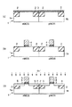
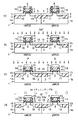
図1〜図3は、本発明の一実施形態に係る半導体装置の製造方法を示す工程断面図である。図4は、従来技術に係る加熱処理が施された比較例としてのシリコン基板の断面を示すTEM写真である。図5は、一実施形態に係る基板予備加熱温度とフラッシュランプの照射エネルギー密度との関係における適正なプロセス条件を示す図である。図6は、比較例に係る基板予備加熱温度とフラッシュランプの照射エネルギー密度との関係における適正なプロセス条件を示す図である。
【0030】
本実施形態では、半導体基板に放射光エネルギーによる加熱処理工程を行う前に、電気的不活性な不純物を半導体基板の全面に対して少なくとも1回イオン注入する。この際、電気的不活性な不純物として、例えばC、Si、Ge、Sn、およびPb等のIV−B族の元素のうち少なくとも1種類の元素を用いる。これにより、半導体基板の転位、欠陥、モフォロジー劣化等のダメージを防ぐ。以下、半導体基板上にCMOSトランジスタを製造する場合を例に挙げて、具体的に説明する。
【0031】
先ず、図1(a)に示すように、通常のCMOSトランジスタの製造方法に従って、半導体基板(シリコン基板)1のnMOS領域1aに図示しないp型well層を、またpMOS領域1bに同じく図示しないn型well層をそれぞれ形成する。続けて、nMOS領域1aおよびpMOS領域1bに素子分離領域2を形成する。この後、素子分離領域2が形成されたシリコン基板(Si基板)1の表面を覆って、例えばシリコン酸化膜(SiO2膜)からなるゲート絶縁膜3を設ける。
【0032】
次に、図1(b)に示すように、ゲート絶縁膜3上の所定の位置にゲート電極となる多結晶シリコン膜(ポリシリコン膜)4を成膜する。続けて、例えばRIE法によりゲート電極4およびゲート絶縁膜3を選択的に加工して、所定の形状に形成する。これにより、シリコン基板1のnMOS領域1a上およびpMOS領域1b上に、ゲート電極4が1個ずつ形成される。
【0033】
次に、図1(c)に示すように、各ゲート電極4の上部およびシリコン基板1の表層部に、シリコン基板1の導電型および導電率に影響を及ぼすおそれが殆ど無い、電気的に不活性な第1の不純物としてのゲルマニウム(Ge)を全面的にイオン注入する。この際、ゲルマニウムイオン(Ge+)は、その加速エネルギーを約1keVに、またドーズ量を約5×1014cm−2に設定される。また、注入されるゲルマニウムの濃度は、1×1019cm−3以上に設定される。これにより、ゲート電極4の上部およびシリコン基板1の表層部に、第1のGe注入領域5が形成される。
【0034】
次に、図2(a)に示すように、Ge注入領域5が形成されたpMOS領域1bおよびpMOS領域1b上のゲート電極4を覆って、レジスト膜6を成膜する。続けて、Ge注入領域5が形成されたnMOS領域1a上のゲート電極4をマスクとして、シリコン基板1のnMOS領域1aの表層部に、第2の不純物としてのn型不純物となる砒素(As)をイオン注入する。この際、砒素イオン(As+)は、その加速エネルギーを約1keVに、またドーズ量を約1×1015cm−2に設定される。このイオン注入により、ゲート電極4に隣接するnMOS領域1aの表層部に、Asを含有するn型の浅い不純物領域7が形成される。この後、pMOS領域1b上のレジスト膜6をエッチングなどにより除去する。
【0035】
次に、図2(b)に示すように、表層部にn型不純物を含有する浅い不純物領域7が形成されたnMOS領域1aおよびnMOS領域1a上のゲート電極4を覆って、レジスト膜8を成膜する。続けて、Ge注入領域5が形成されたpMOS領域1b上のゲート電極4をマスクとして、シリコン基板1のpMOS領域1bの表層部に、第2の不純物としてのp型不純物となるホウ素(B)をイオン注入する。この際、ホウ素イオン(B+)は、その加速エネルギーを約0.2keVに、またドーズ量を約1×1015cm−2に設定される。このイオン注入により、ゲート電極4に隣接するpMOS領域1bの表層部に、Bを含有するp型の浅い不純物領域9が形成される。この後、nMOS領域1a上のレジスト膜8をエッチングなどにより除去する。
【0036】
次に、図2(c)に示すように、シリコン基板1を予め約400℃まで加熱(基板予備加熱)した状態で、シリコン基板1および各ゲート電極4の表面に向けて図示しないキセノン(Xe)フラッシュランプの光を照射する。これにより、シリコン基板1等にアニール処理を施す。このアニール処理により、nMOS領域1aの表層部にイオン注入されたn型不純物(As)、およびpMOS領域1bの表層部にイオン注入されたp型不純物(B)が、それぞれが活性化される。それとともに、nMOS領域1aの表層部に形成された浅い不純物領域7、およびpMOS領域1bの表層部に形成された浅い不純物領域9の、それぞれの内部の結晶欠陥が修復される。この結果、nMOS領域1aの表層部に、ゲート電極4に隣接するn型の浅いソース・ドレイン拡散層(エクステンション領域)10を得る。それとともに、pMOS領域1bの表層部に、ゲート電極4に隣接するp型浅いソース・ドレイン拡散層11を得る。なお、本実施形態では、前述した基板予備加熱を、図示しないホットプレートにより行うこととする。
【0037】
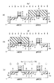
次に、図3(a)に示すように、例えばCVD法により、浅いソース・ドレイン拡散層10,11が形成されたシリコン基板1および各ゲート電極4の表面を覆って、シリコン窒化膜(SiN膜)12およびシリコン酸化膜(SiO2膜)13を順次堆積させる。続けて、例えばRIE法により、SiN膜12およびSiO2膜13を各ゲート電極4の側部付近にのみ選択的に残置させる。これにより、各ゲート電極4の側部を覆って、SiN膜12およびSiO2膜13の2層構造からなる側壁スペーサ(ゲート側壁膜)14が設けられる。
【0038】
次に、図3(b)に示すように、側壁スペーサ14が設けられた各ゲート電極4の上部およびシリコン基板1の表層部などに、Geを全面的にイオン注入する。この際、ゲルマニウムイオン(Ge+)は、その加速エネルギーを約1keVに、またドーズ量を約5×1014cm−2に設定される。また、注入されるゲルマニウムの濃度は、1×1019cm−3以上に設定される。これにより、各ゲート電極4の上部およびシリコン基板1の表層部などに、第2のGe注入領域15が形成される。
【0039】
次に、図3(c)に示すように、各ゲート電極4および側壁スペーサ14などをマスクとして、第2のGe注入領域15が形成されたシリコン基板1のnMOS領域1aおよびpMOS領域1bのそれぞれの表層部に、第3の不純物をイオン注入する。具体的には、nMOS領域1aには、n型不純物となるリン(P)をイオン注入する。この際、リンイオン(P+)は、その加速エネルギーを約15keVに、またドーズ量を約5×1015cm−2に設定される。このイオン注入により、nMOS領域1aの表層部のゲート電極4の端部から離間した位置に、Pを含有する深いn型の不純物領域16が形成される。また、このイオン注入により、nMOS領域1a上のゲート電極4および側壁スペーサ14の上部にも、Pがイオン注入される。
【0040】
また、pMOS領域1bには、p型不純物となるホウ素(B)をイオン注入する。この際、ホウ素イオン(B+)は、その加速エネルギーを約4keVに、またドーズ量を約5×1015cm−2に設定される。このイオン注入により、pMOS領域1bの表層部のゲート電極4の端部から離間した位置に、Bを含有する深いp型の不純物領域17が形成される。また、このイオン注入により、pMOS領域1b上のゲート電極4および側壁スペーサ14の上部にも、Bがイオン注入される。
【0041】
次に、図3(d)に示すように、シリコン基板1を予め約400℃まで加熱(基板予備加熱)した状態で、シリコン基板1および各ゲート電極4の表面に向けて図示しないキセノン(Xe)フラッシュランプの光を照射する。これにより、シリコン基板1等にアニール処理を施す。この際、アニール条件として、Xeフラッシュランプの発光時間(照射時間)、すなわちXeフラッシュランプのパルス幅を約1msに、また照射エネルギー密度を約35J/cm2に設定する。このアニール処理により、nMOS領域1aの表層部にイオン注入されたn型不純物(P)、およびpMOS領域1bの表層部にイオン注入されたp型不純物(B)が、それぞれが活性化される。それとともに、nMOS領域1aの表層部に形成されたn型の深い不純物領域16、およびpMOS領域1bの表層部に形成されたp型の深い不純物領域17の、それぞれの内部の結晶欠陥が修復される。この結果、nMOS領域1aの表層部のゲート電極4の端部から離間した位置に、n型の深いソース・ドレイン拡散層18が形成される。それとともに、pMOS領域1bの表層部のゲート電極4の端部から離間した位置に、p型の深いソース・ドレイン拡散層19が形成される。なお、本実施形態では、前述した基板予備加熱を、図示しないホットプレートにより行うこととする。
【0042】
以後、図示および詳しい説明は省略するが、例えば常圧CVD法により、成膜温度を約400℃に設定して、各ゲート電極4を覆って、シリコン基板1の表面上に全面的に層間絶縁膜としてのシリコン酸化膜(SiO2膜)を形成する。この後、シリコン酸化膜中の所定の箇所に図示しないコンタクトホール等を開孔したり、ソース・ドレイン電極や配線等を形成したりする。これにより、nMOSトランジスタ20aおよびpMOSトランジスタ20bからなる所望のCMOSトランジスタ20を得る。この後、さらに所定の工程を経て、CMOSトランジスタ20を備える所望の半導体装置を得る。
【0043】
次に、以上説明した本実施形態に係る加熱処理が施された半導体基板と、本実施形態に対する比較例として従来技術に係る加熱処理が施された半導体基板とを比較する。比較例としての半導体基板(シリコン基板)は、前述した本実施形態と異なり、図1(c)および図3(b)に示したGe等のIV−B族元素の全面的なイオン注入工程が省略されている。そして、As、B、P等がイオン注入された後、直ちにXeフラッシュランプの光線が本実施形態と同等の条件下で照射されている。
【0044】
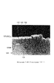
図4に、比較例のサンプルとして、シリコン基板101の断面を図示しない微分干渉顕微鏡および透過型電子顕微鏡(Transmission Electron Microscopy:TEM)によって観察した写真を示す。シリコン基板101の表層部には、能動領域(Active area)102と、シリコン酸化膜(SiO2膜)103が埋め込まれた浅溝の素子分離(Shallow Trench Isolation:STI)領域104とからなる、ライン・アンド・スペースパターン(Line/Space pattern)が形成されている。図4に示す写真によれば、シリコン基板101は、転移、積層欠陥、溶融に伴う表面平坦度の劣化など、様々な損傷を受けていることが分かる。これに対して、本実施形態に係る半導体基板(シリコン基板)1のサンプルは、本発明者らが行った観察によれば、図示は省略するが、比較例のシリコン基板101に見られるような損傷は確認されなかった。
【0045】
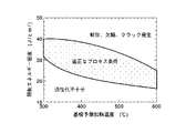
図5に、本実施形態に係る基板予備加熱温度とフラッシュランプの照射エネルギー密度との関係における適正なプロセス条件(プロセスウィンドウ)を示す。また、図6には、比較例に係る基板予備加熱温度とフラッシュランプの照射エネルギー密度との関係における適正なプロセス条件(プロセスウィンドウ)を示す。これら図5および図6によれば、本実施形態および比較例ともに、基板予備加熱温度を高くするにつれて、不純物の活性化に必要な照射エネルギー密度を低く抑えることができることが分かる。ところが、基板予備加熱温度を高くするにつれて、転移、欠陥、あるいはクラックなどが基板中に発生する照射エネルギー密度も小さくなることが分かる。すなわち、本実施形態および比較例ともに、基板予備加熱温度を高くするにつれて、基板が損傷を受け易くなることが分かる。
【0046】
ただし、図5および図6から明らかなように、本実施形態は、比較例に比べてプロセスウィンドウがはるかに広く、プロセスマージンが大きい。すなわち、本実施形態は、比較例に比べて基板が損傷を受け難く、かつ、不純物を活性化させ易い。また、シリコン基板の面内均一性について本発明者らが行った実験によれば、比較例では拡散層抵抗のばらつきが大きく、σ(標準偏差/平均値×100%)が約10%であった。これに対して、本実施形態では、σが1%未満に抑えられていることが分かった。以下、この理由について、詳しく考察する。
【0047】
Xeフラッシュランプは、シリコン(Si)の吸収端よりも短波長側である可視光領域を主要な発光領域(ピーク波長領域:約300〜500nm)とする白色光ランプである。これに加えて、Xeフラッシュランプは、ミリ秒オーダーで高速昇降温が可能である。このため、Xeフラッシュランプによる加熱効率は、基板の表面状態、すなわち基板および基板上に成膜した膜の材質(光吸収係数)などに大きく依存する。前述した比較例では、単結晶のシリコン(Si)からなるSi基板101上に、素子分離領域104を構成するSiO2膜103、ゲート電極となる図示しないpoly−Si層、ならびにゲート電極の側壁スペーサを構成する図示しないSiO2膜およびSiN膜などが存在している。このため、Si基板101上の表面状態や光吸収係数などが場所によって異なっている。このような条件下でフラッシュランプアニールを行うと、異種材質間で局所的な温度むらが生じ、熱応力が局所的に発生する。また、Si基板101と素子分離領域104を構成するSiO2膜103との屈折率の差異により、SiO2膜103がレンズ効果を発揮して、Si基板101を局所的に加熱するおそれもある。これらの理由により、前述した比較例では、Si基板101に転位や積層欠陥等のダメージが入り易いと考えられる。
【0048】
これに対して、本実施形態では、フラッシュランプアニールを行う前に、GeをSi基板1に全面的にイオン注入する。これにより、異種材料間で表面の光吸収係数が略均一化されて、加熱効率の差が縮まると考えられる。それとともに、SiとSiO2との屈折率の差異も縮められて、局所的な加熱が抑制されると考えられる。これらにより、Si基板1の面内における熱特性の均一性が向上されて、異種材料間での温度差による熱応力の発生が抑制されると考えられる。また、Si基板1の表面は、Geがイオン注入されることによって光吸収量が増大する。この結果、エクステンション領域10,11およびソース・ドレイン領域18,19の不純物の活性化が効率良く行われる。これにより、不純物の活性化に必要な照射エネルギーを低減させることができる。ひいては、Si基板1中に熱応力が発生するおそれをさらに抑制して、生産歩留まりを向上させることができる。また、良質な浅いソース・ドレイン拡散層10,11および良質な深いソース・ドレイン拡散層18,19を効率良く容易に形成して、品質および信頼性が向上されたCMOSトランジスタ20を設けることができる。
【0049】
また、レーザーアニール法では、基板にダメージを与えずに光源のエネルギーを基板に均一に吸収させるために、図示は省略するが、例えばpoly−Si膜、Ti膜、あるいはTiN膜等の光吸収膜を基板上に設ける技術が従来から知られている。しかしながら、この方法は、光源から照射されるエネルギーを光吸収膜に一旦吸収させた後、そのエネルギーを下地の膜あるいは基板に熱伝導させて加熱するものである。このため、エネルギーの伝達にロスが多く、過剰なエネルギーが必要となるので、効率的な加熱処理を行うことが困難である。また、アニール終了後、役目を終えた光吸収膜を基板から剥離させる必要があるため、工程数の増加に繋がる。さらに、仮に基板からの光吸収膜の剥離工程が適正に実行されず、膜残りやオーバーエッチングなどが生じた場合には、その基板を備える製品の品質や信頼性の劣化を招くおそれが大きい。
【0050】
これに対して、本実施形態では、シリコン基板1等に加熱処理を施すのに先立って、Geをシリコン基板1等に全面的にイオン注入する。Geは電気的に不活性であるため、他の物質の電気特性に悪影響を及ぼす心配が殆ど無い。それとともに、Geのイオン注入工程を、不純物拡散領域へ不純物をイオン注入する際のプリアモルファス化工程として、そのまま適用することができる。すなわち、本実施形態によれば、レーザーアニール法においても効率的な加熱処理を行うことが可能となり、光源の照射エネルギーを節約することができる。それとともに、浅い不純物拡散領域における不純物の適正なプロファイルを、容易に得ることができる。
【0051】
このように、本実施形態によれば、加熱用の光源の種類に拘らず、転位、欠陥、スリップ、クラック、モフォロジー劣化、および溶融等のダメージを半導体基板1に殆ど与えること無く光線を用いる加熱処理を行って、基板1内に浅い不純物拡散層を高濃度で形成することができる。ひいては、基板1上に設けられるデバイス特性の面内均一性の改善、およびデバイスの製造プロセスの安定化などを図って、次世代LSIの性能を十分に発揮させることができる微細なMOSトランジスタを、容易に製造することができる。
【0052】
以上説明したように、この一実施形態によれば、光線を用いる加熱処理を行うのに先立って、シリコン基板1およびその上に設けられている様々な異種材料に、シリコン基板1の導電型および導電率に影響を及ぼすおそれが殆ど無い、電気的に不活性なGeを全面的にイオン注入する。これにより、シリコン基板1等の電気的特性を劣化させることなく、各種のデバイスパターン等を構成している複数の膜等の表層部における光の吸収係数を略均一化できる。この結果、各種素子の疎密などによる加熱むらや、そのような加熱むらにより発生する熱応力を抑制することができる。また、半導体基板1等の表層部は、電気的に不活性な不純物がドーピングされることによって、光吸収量すなわち光りの吸収効率が増大する。これにより、電気的に活性な不純物を活性化させる際に必要な光源の照射エネルギーを低減させることができる。この結果、半導体基板1内に熱応力が発生するおそれをさらに抑制して、半導体基板1を具備する半導体装置の品質、信頼性、および生産歩留まりを向上させることができる。
【0053】
また、この一実施形態によれば、半導体基板1等のアニール処理を効率良く行うことができるので、プロセスウィンドウを広げることができる。すなわち、半導体基板1への加熱処理を含めた半導体装置の製造プロセスを安定化させることができる。さらに、電気的に活性な不純物を十分に活性化させて半導体素子の電気特性のばらつきを抑制できるとともに、半導体素子の微細化も容易になる。これにより、高性能、高品質、かつ信頼性が高いCMOSトランジスタ20を高い集積度で製造することができる。
【0054】
このように、本実施形態に係る半導体装置は、これが備える半導体基板に熱応力による変形や損傷が生じたり、加熱むらによる品質劣化が生じたりするおそれが殆ど無くされているとともに、半導体基板等の電気的特性の劣化が殆ど無いので、品質、信頼性、および歩留まりが向上されている。また、本実施形態に係る半導体装置の製造方法によれば、半導体基板等の電気的特性が劣化されたり、半導体基板に熱応力による変形や損傷が生じたり、あるいは半導体基板に加熱むらによる品質劣化が生じたりするおそれを殆ど無くして、品質、信頼性、および歩留まりが向上された半導体装置を容易に製造することができる。さらに、良質な浅いソース・ドレイン拡散層10,11および良質な深いソース・ドレイン拡散層18,19を効率良く容易に形成して、品質および信頼性が向上されたCMOSトランジスタ20を具備するとともに、歩留まりが向上された半導体装置を効率良く容易に製造することができる。
【0055】
なお、本発明に係る半導体装置およびその製造方法は、前述した一実施形態には制約されない。本発明の趣旨を逸脱しない範囲で、それらの構成または工程などの一部を種々様々な設定に変更したり、あるいはそれらの構成や工程などを適宜、適当に組み合わせて用いたりして実施することができる。
【0056】
例えば、前述した一実施形態では、深いソース・ドレイン拡散層18,19を形成する際に、基板予備加熱温度を約400℃に設定した。それとともに、Xeフラッシュランプの照射エネルギー密度を約35J/cm2に設定してアニール処理を行い、不純物を活性化させた。しかし、この場合の基板予備加熱温度および照射エネルギー密度は、その値には限定されない。本発明者らが行った実験によれば、基板予備加熱温度が約600℃以下、かつ、照射エネルギー密度が約100J/cm2以下であれば、基板予備加熱温度および照射エネルギー密度を適宜、適正な温度に設定しても、前述した一実施形態と同等の効果を得ることができることが分かっている。この際、フラッシュランプのパルス幅(発光時間、照射時間)も、約1msには限定されない。フラッシュランプのパルス幅は、約100ms以下であれば適宜、適正な値に設定しても、前述した一実施形態と同等の効果を得ることができることが分かっている。
【0057】
ただし、本発明者らが行った実験によれば、基板予備加熱温度を約200〜550℃、フラッシュランプの照射エネルギー密度を約10〜60J/cm2の範囲内に設定すると、より良い効果を得ることができることが分かっている。具体的には、基板予備加熱温度を約550℃以下に設定することにより、アモルファス状態である不純物注入領域がフラッシュランプの照射前に中途半端に結晶化するのを抑制することができる。これにより、不純物注入領域内の残留欠陥の発生を防ぐことができる。また、基板予備加熱温度を200℃以下に設定すると、不純物を十分に活性化させるために約60J/cm2以上の照射エネルギー密度が必要となる。すると、Si基板1内に熱によるダメージが発生し易くなる。したがって、基板予備加熱温度を約200℃以上に設定することにより、Si基板1内に熱によるダメージが発生するおそれを殆ど無くすことができる。その上で、フラッシュランプの照射エネルギー密度を約10〜60J/cm2内に設定することにより、熱によるSi基板1内のダメージ発生を防ぐことができるとともに、フラッシュランプの寿命劣化を抑制することができる。
【0058】
また、半導体基板1の予備加熱は、前述したホットプレートより行う必要は無い。例えば、各種加熱ランプ、あるいはレーザー光線などを用いても、ホットプレートと同様の効果を得ることができる。この際、加熱ランプとしては、例えば水素ランプ、キセノンランプ、あるいはハロゲンランプなどを用いることができる。
【0059】
また、電気的に不活性な第1の不純物は、電気的に活性な第2の不純物(導電型を決定する不純物)をシリコン基板1にイオン注入する前に、シリコン基板1に全面的にイオン注入されるとは限らない。第2の不純物を活性化させる加熱処理を施す前であれば、第2の不純物をシリコン基板1にイオン注入した後に、第1の不純物をシリコン基板1に全面的にイオン注入しても、前述した一実施形態と同等の効果を得ることができる。また、第1の不純物のイオン注入は、1回の加熱処理に対して1回行うとは限らない。1回の加熱処理に対して、第1の不純物を複数回イオン注入することにより、前述した一実施形態と同等もしくはそれ以上の効果を得ることができる。また、第1の不純物は、Geには限定されない。電気的に不活性な第1の不純物としては、例えばC、Si、Sn、あるいはPb等、IV−B族の元素のうち少なくとも1種類の元素を用いれば、前述した一実施形態と同等の効果を得ることができる。また、第1の不純物のイオン注入を複数回行う場合、IV−B族の元素のうち少なくとも1種類の元素であれば、各回ごとに注入する不純物の種類を変えても前述した一実施形態と同等の効果を得ることができる。
【0060】
また、電気的に不活性な第1の不純物をシリコン基板1にイオン注入する際の濃度は、前述した1×1019cm−3以上には限られない。シリコン基板1の表層部をアモルファス化できる濃度であれば、より高い濃度に設定しても構わない。本発明者らが行った実験によれば、第1の不純物をシリコン基板1にイオン注入する際の濃度を、前述した1×1020cm−3以上に設定することにより、シリコン基板1の表層部をより良質なアモルファス状態にできることが分かっている。なお、第1の不純物をシリコン基板1にイオン注入する際の加速条件は、pn接合のリーク特性を劣化させない範囲であれば適宜、適正な値に設定して構わない。
【0061】
また、前述した一実施形態では、シリコン基板1上にCMOSトランジスタ20を設ける場合を例に挙げて説明したが、それだけには限られない。例えば、シリコン基板1上にnMOSトランジスタ20aのみを設ける場合には、導電型を考慮する必要が無い。この場合、電気的に活性な不純物であるAsやP等のV−B族の元素のうち少なくとも1種類の元素のみをシリコン基板1に全面的にイオン注入しても構わない。また、シリコン基板1上にpMOSトランジスタ20bのみを設ける場合にも、導電型を考慮する必要が無い。この場合、電気的に活性な不純物であるB等のIII−B族の元素のうち少なくとも1種類の元素のみをシリコン基板1に全面的にイオン注入しても構わない。これらのように、導電型を考慮する必要が無い場合、導電型が同じであれば、電気的に活性な不純物をシリコン基板1に全面的にイオン注入しても、前述した一実施形態と同等の効果を得ることができる。
【0062】
また、前述した一実施形態において、nMOS領域1aに注入されるn型不純物となる元素は、AsやPには限られない。n型不純物として、V−B族の元素のうち少なくとも1種類の元素を用いれば、前述した一実施形態と同等の効果を得ることができる。同様に、pMOS領域1bに注入されるp型不純物となる元素は、Bには限られない。p型不純物として、III−B族の元素のうち少なくとも1種類の元素を用いれば、前述した一実施形態と同等の効果を得ることができる。
【0063】
また、浅いソース・ドレイン拡散層10,11を形成する際のアニール工程は、前述したフラッシュランプアニールには限定されない。フラッシュランプの代わりに、ハロゲンランプを用いたRTA処理でも前述した一実施形態と同等の効果を得ることができる。また、本発明者らが行った実験によれば、浅いソース・ドレイン拡散層10,11を形成する際のアニール条件として、基板温度を900℃以下に、加熱時間を10秒以下に設定すると、より良質な拡散層10,11を形成できることが分かっている。これは、シリコン基板1を短時間で高温に加熱することにより、不純物元素が基板1の深い位置まで拡散されること無く活性化されるとともに、不純物領域10,11中の結晶欠陥が回復されるためであると考えられる。
【0064】
また、前述した一実施形態では、加熱光源(アニール装置)としてXeフラッシュランプを使ったフラッシュランプアニール法について説明したが、これに限定されるものでは無い。加熱光源としては、例えば水銀ランプ、水素ランプ、メタルハライドランプ、希ガスランプ、エキシマレーザー、あるいはYAGレーザー等、近赤外領域から紫外領域に亘って発光する光源を用いることができる。また、従来のハロゲンランプを加熱光源として用いることができるのはもちろんである。
【0065】
さらに、前述した一実施形態では、浅いソース・ドレイン拡散層10,11、すなわちエクステンション領域10,11の形成と、深いソース・ドレイン拡散層18,19の形成とを例に挙げて説明したが、これらに限定されるものでは無い。本発明は、チャネル領域の形成やゲート酸化膜の形成、あるいは極めて短時間の加熱処理が必要な、その他の様々な加熱工程にも十分に適用可能であるのはもちろんである。
【0066】
【発明の効果】
本発明の一態様に係る半導体装置の製造方法によれば、半導体基板に光による加熱処理を施すのに先立って、電気的に不活性な第1の不純物を半導体基板に全面的に注入する。これにより、半導体基板等の電気的特性が劣化されたり、熱応力による変形や損傷が生じたり、あるいは加熱むらによる品質劣化が生じたりするおそれを殆ど無くして、半導体基板に光による加熱処理を施すことができる。したがって、本発明の一態様に係る半導体装置の製造方法によれば、電気的特性が殆ど劣化されること無く、加熱処理に用いられる光の吸収効率の向上および均一化が図られ、加熱むらや熱応力の発生を抑制されて光による加熱処理が施された半導体基板を具備し、品質、信頼性、および歩留まりが向上された半導体装置を効率良く容易に製造できる。
【0067】
また、本発明の他の態様に係る半導体装置の製造方法によれば、半導体基板に光による加熱処理を施してソース・ドレイン拡散層を形成するのに先立って、電気的に不活性な第1の不純物を半導体基板に全面的に注入するとともに、半導体基板の所定の領域に電気的に活性な第2の不純物を注入する。これにより、半導体基板等の電気的特性が劣化されたり、熱応力による変形や損傷が生じたり、あるいは加熱むらによる品質劣化が生じたりするおそれを殆ど無くして、光による加熱処理により良質なソース・ドレイン拡散層を効率良く容易に形成することができる。したがって、本発明の他の態様に係る半導体装置の製造方法によれば、電気的特性が殆ど劣化されること無く、加熱処理に用いられる光の吸収効率の向上および均一化が図られて加熱むらや熱応力の発生を抑制された半導体基板に、光による加熱処理により良質なソース・ドレイン拡散層を効率良く容易に形成して、品質および信頼性が向上されたトランジスタを具備するとともに、歩留まりが向上された半導体装置を効率良く容易に製造できる。
【0068】
また、本発明の他の態様に係る半導体装置においては、これが備える半導体基板に電気的に不活性な第1の不純物が半導体基板に全面的に注入されて、半導体基板の光の吸収係数や屈折率が全面的に略均一化された後、半導体基板に加熱処理が施されている。すなわち、半導体基板等の電気的特性が劣化されたり、熱応力による変形や損傷が生じたり、あるいは加熱むらによる品質劣化が生じたりするおそれを殆ど無くされて、半導体基板に光による加熱処理が施されている。したがって、本発明の一態様に係る半導体装置は、電気的特性が殆ど劣化されること無く、加熱処理に用いられる光の吸収効率の向上および均一化が図られ、加熱むらや熱応力の発生を抑制されて光による加熱処理が施された半導体基板を具備し、品質、信頼性、および歩留まりが向上されている。
【0069】
さらに、本発明の他の態様に係る半導体装置においては、これが備える半導体基板に電気的に不活性な第1の不純物が全面的に注入されるとともに、所定の導電型を有する電気的に活性な第2の不純物が注入された後、光による加熱処理が施されて第2の不純物が活性化され、ソース・ドレイン拡散層が形成されている。すなわち、半導体基板等の電気的特性が劣化されたり、熱応力による変形や損傷が生じたり、加熱むらによる品質劣化が生じたりするおそれを殆ど無くされて、光による加熱処理により良質なソース・ドレイン拡散層が形成されている。したがって、本発明の他の態様に係る半導体装置は、電気的特性が殆ど劣化されること無く、加熱処理に用いられる光の吸収効率の向上および均一化が図られて加熱むらや熱応力の発生を抑制された半導体基板に、光による加熱処理により良質なソース・ドレイン拡散層が形成されて、品質および信頼性が向上されたトランジスタを具備するとともに、歩留まりが向上されている。
【図面の簡単な説明】
【図1】一実施形態に係る半導体装置の製造方法を示す工程断面図。
【図2】一実施形態に係る半導体装置の製造方法を示す工程断面図。
【図3】一実施形態に係る半導体装置の製造方法を示す工程断面図。
【図4】従来技術に係る加熱処理が施された比較例としてのシリコン基板の断面を示すTEM写真。
【図5】一実施形態に係る基板予備加熱温度とフラッシュランプの照射エネルギー密度との関係における適正なプロセス条件を示す図。
【図6】比較例に係る基板予備加熱温度とフラッシュランプの照射エネルギー密度との関係における適正なプロセス条件を示す図。
【符号の説明】
1…シリコン基板(半導体基板)、3…ゲート絶縁膜(シリコン酸化膜、SiO2膜)、4…ゲート電極(多結晶シリコン膜、ポリシリコン膜)、7…n型の浅い不純物領域(ゲート電極に隣接する領域)、9…p型の浅い不純物領域(ゲート電極に隣接する領域)、10…n型の浅いソース・ドレイン拡散層(n型のエクステンション領域)、11…p型の浅いソース・ドレイン拡散層(p型のエクステンション領域)、12…シリコン窒化膜(SiN膜、ゲート側壁膜)、13…シリコン酸化膜(SiO2膜、ゲート側壁膜)、14…ゲート側壁膜(側壁スペーサ)、16…n型の深い不純物領域(ゲート側壁膜に隣接する領域)、17…p型の深い不純物領域(ゲート側壁膜に隣接する領域)、18…n型の深いソース・ドレイン拡散層、19…p型の深いソース・ドレイン拡散層、20…CMOSトランジスタ、20a…nMOSトランジスタ、20b…pMOSトランジスタ[0001]
BACKGROUND OF THE INVENTION
The present invention relates to a semiconductor device including a semiconductor substrate subjected to heat treatment and a method for manufacturing the same, and more particularly to a semiconductor device including a semiconductor substrate in which an impurity diffusion region or the like is formed in a surface layer portion by heat treatment and the manufacture thereof. Regarding the method.
[0002]
[Prior art]
The performance improvement of LSI can be realized by increasing the degree of integration, that is, by miniaturizing elements constituting a semiconductor. In recent years, the scale of integrated circuits has been increasing, and along with this, miniaturization of elements has been further increased. As the device size is reduced, the formation of a shallow pn junction is becoming more important.
[0003]
As a method for forming a shallow impurity diffusion region, for example, a method in which a predetermined ion is implanted into a silicon (Si) substrate with low acceleration energy and then an annealing process optimized for the Si substrate is performed (for example,
[0004]
Therefore, in recent years, in order to solve these problems, laser annealing and flash lamp annealing have been studied as methods for instantaneously supplying energy necessary for impurity activation. However, since the laser beam has good directivity, interference easily occurs and the irradiation area is also limited. For this reason, it is difficult to maintain the uniformity and reproducibility of the irradiation energy for a wafer (substrate) having a large area. Further, it is difficult to adjust the intensity of the laser beam, and it is difficult to obtain an intensity suitable for annealing. For this reason, there is a possibility that the energy density per unit time or unit area becomes too high and the surface of the semiconductor substrate is melted. Thus, it has been pointed out that the general laser annealing method may deteriorate the morphology of the semiconductor substrate surface after the impurity activation treatment.
[0005]
On the other hand, in the flash lamp annealing method that has recently attracted attention, the light emission of the Xe flash lamp, which is a heat source, is completed within an extremely short time of several hundred μmsec to several msec. As a result, the impurity ions can be activated without substantially changing the distribution of the impurity ions implanted into the semiconductor layer. In addition, heat treatment can be performed all over the entire surface of the semiconductor substrate having a large area, and throughput is high. However, in the flash lamp annealing method, there is a concern that a large irradiation area and a high-speed temperature increase / decrease feature cause a large thermal stress on the semiconductor substrate. In particular, poly-Si, SiO 2 In the case of a wafer in which a pattern is formed on the surface by a plurality of types of films such as SiN, uneven heating tends to occur between the types of films. When such heating unevenness occurs, damage such as dislocations and defects is likely to occur on the wafer. As a result, the production yield tends to decrease. In such a case, damage to the substrate can be avoided by lowering the substrate preheating temperature or the irradiation energy of the flash lamp, but sufficient activation of impurities cannot be expected. As described above, the general flash lamp annealing method has a problem in that the process window (process margin) in the manufacturing process of the semiconductor element is narrow.
[0006]
[Patent Document 1]
JP 2002-141298 A
[0007]
[Patent Document 2]
JP 2002-246328 A
[0008]
[Patent Document 3]
JP 2002-198322 A
[0009]
[Patent Document 4]
Japanese Patent Laid-Open No. 2002-175772
[0010]
[Patent Document 5]
JP 10-26772 A
[0011]
[Patent Document 6]
USP 6,417,515
[0012]
[Problems to be solved by the invention]
As described above, when the impurity diffusion layer is formed in the surface layer portion of the substrate, various problems may occur in the substrate regardless of the heat treatment method. In particular, the problem that deformation or damage due to thermal stress occurs in the substrate or quality deterioration due to uneven heating occurs in the substrate or the like is not limited to the case where an impurity diffusion layer is formed on the substrate, but when the substrate is subjected to heat treatment. It can happen at any time.
[0013]
The present invention has been made to solve the problems as described above, and the object of the present invention is to improve the absorption efficiency of light used for heat treatment without almost deteriorating electrical characteristics. To provide a semiconductor device that has a semiconductor substrate that is uniformized and that is subjected to heat treatment with light while suppressing generation of uneven heating and thermal stress, and has improved quality, reliability, and yield. is there. In addition, heat treatment with light is applied to a semiconductor substrate in which the generation efficiency and uniformity of light used for heat treatment are improved and the generation of uneven heating and thermal stress is suppressed with almost no deterioration in electrical characteristics. It is an object of the present invention to provide a semiconductor device in which a high-quality source / drain diffusion layer is formed, a transistor with improved quality and reliability, and a yield is improved. At the same time, it is an object of the present invention to provide a method for manufacturing a semiconductor device capable of manufacturing such a semiconductor device efficiently and easily.
[0014]
[Means for Solving the Problems]
In order to solve the above problems, a method for manufacturing a semiconductor device according to one embodiment of the present invention includes a step of entirely implanting an electrically inactive first impurity into one main surface of a semiconductor substrate; And a step of performing heat treatment with light on the semiconductor substrate into which one impurity has been implanted.
[0015]
In this method of manufacturing a semiconductor device, a first impurity that is electrically inactive is implanted into the entire surface of the semiconductor substrate prior to heat treatment of the semiconductor substrate with light. That is, prior to performing heat treatment with light on the semiconductor substrate, the first impurity which hardly affects the conductivity type and conductivity of the semiconductor substrate or the like is implanted into the semiconductor substrate over the entire surface. As a result, the semiconductor substrate can be subjected to heat treatment with light in a state in which the light absorption coefficient and refractive index of the semiconductor substrate are substantially uniform over the entire surface without substantially degrading the electrical characteristics of the semiconductor substrate or the like. . In other words, the heat treatment by light is applied to the semiconductor substrate in a state in which the generation of thermal stress due to uneven heating and local heating is suppressed with almost no deterioration in electrical characteristics of the semiconductor substrate and the like, and almost no difference in heating efficiency. Can be applied. In addition, by implanting the first impurity into the semiconductor substrate, the semiconductor substrate can be made amorphous to increase the light absorption efficiency (absorption amount). Thereby, the irradiation energy of light required for the heat treatment can be reduced, the heat stress generated in the semiconductor substrate can be suppressed, and the heat treatment with light can be performed.
[0016]
As described above, in the method for manufacturing a semiconductor device according to one embodiment of the present invention, the electrical characteristics of the semiconductor substrate or the like are hardly deteriorated, the semiconductor substrate is deformed or damaged by thermal stress, or the heating is uneven. The heat treatment by light can be efficiently and easily performed on the semiconductor substrate with almost no risk of quality degradation due to.
[0017]
In order to solve the above problems, a method of manufacturing a semiconductor device according to another aspect of the present invention includes a step of providing a gate electrode having a gate insulating film on one main surface of a semiconductor substrate, and the gate electrode is provided. A first impurity that is electrically inactive is entirely injected into one main surface of the semiconductor substrate, and a predetermined area is formed in a region adjacent to the gate electrode of the semiconductor substrate using the gate electrode as a mask. A step of implanting an electrically active second impurity having a conductivity type, and a heat treatment by light on the semiconductor substrate into which the first impurity and the second impurity have been implanted, thereby performing the second treatment. Activating impurities to form a shallow source / drain diffusion layer having the predetermined conductivity type; providing a gate sidewall film around the gate electrode; and providing the gate sidewall film. In addition, the first impurity is entirely implanted into one main surface of the semiconductor substrate, and the gate electrode and the gate sidewall film are used as a mask in a region adjacent to the gate sidewall film in the semiconductor substrate. A step of injecting the second impurity, and applying the heat treatment to the semiconductor substrate into which the first impurity and the second impurity have been implanted to activate the second impurity, and thereby the predetermined conductivity And a step of forming a deep source / drain diffusion layer continuous with the shallow source / drain diffusion layer.
[0018]
In this method of manufacturing a semiconductor device, a first impurity that is electrically inactive is formed prior to forming a shallow source / drain diffusion layer and a deep source / drain diffusion layer by subjecting a semiconductor substrate to heat treatment with light. Is implanted into the entire surface of the semiconductor substrate, and an electrically active second impurity is implanted into a predetermined region of the semiconductor substrate. That is, there is almost no risk of affecting the conductivity type and conductivity of the semiconductor substrate or the like prior to forming the shallow source / drain diffusion layer and the deep source / drain diffusion layer by subjecting the semiconductor substrate to heat treatment with light. A first impurity is implanted into the entire surface of the semiconductor substrate, and an electrically active second impurity is implanted into a predetermined region of the semiconductor substrate. As a result, the semiconductor substrate is subjected to heat treatment with light in a state where the light absorption coefficient and refractive index of the semiconductor substrate are substantially uniform over the entire surface without substantially degrading the electrical characteristics of the semiconductor substrate, etc. A drain diffusion layer can be formed. In other words, the heat treatment by light is applied to the semiconductor substrate in a state in which the generation of thermal stress due to uneven heating and local heating is suppressed with almost no deterioration in electrical characteristics of the semiconductor substrate and the like, and almost no difference in heating efficiency. As a result, a source / drain diffusion layer can be formed.
[0019]
In addition, by implanting the first impurity into the semiconductor substrate, the semiconductor substrate can be made amorphous to increase the light absorption efficiency (absorption amount). Thereby, the irradiation energy of light required for the heat treatment can be reduced, the thermal stress generated in the semiconductor substrate can be suppressed, and the heat treatment with light can be performed to form the source / drain diffusion layers. That is, while suppressing the thermal stress generated in the semiconductor substrate, the electrically active second impurity can be efficiently activated to form a high-quality source / drain diffusion layer.
[0020]
As described above, the method for manufacturing a semiconductor device according to another aspect of the present invention hardly deteriorates the electrical characteristics of the semiconductor substrate or the like, causes deformation or damage due to thermal stress in the semiconductor substrate, or causes uneven heating. Therefore, it is possible to efficiently and easily form a high-quality source / drain diffusion layer on the semiconductor substrate by heat treatment with light.
[0021]
In order to solve the above-described problem, a semiconductor device according to another aspect of the present invention is a semiconductor in which an electrically inactive first impurity is entirely implanted and then subjected to heat treatment with light. A substrate is provided.
[0022]
In this semiconductor device, before the heat treatment with light is performed on the semiconductor substrate, the electrically inactive first impurity is entirely implanted into the semiconductor substrate. That is, prior to performing heat treatment with light on the semiconductor substrate, the first impurity having almost no possibility of affecting the conductivity type and conductivity of the semiconductor substrate or the like is implanted into the semiconductor substrate. As a result, the semiconductor substrate or the like is subjected to heat treatment with light in a state in which the light absorption coefficient and refractive index are substantially uniform over the entire surface with almost no deterioration in electrical characteristics. In other words, semiconductor substrates and the like are heated by light in a state in which the electrical characteristics are hardly deteriorated, the difference in heating efficiency is almost eliminated, and the generation of thermal stress due to uneven heating and local heating is suppressed. Processing is performed. Further, the semiconductor substrate is made amorphous by the implantation of the first impurity, and the light absorption efficiency (absorption amount) is increased. Thereby, the irradiation energy of light required for heat processing can be reduced and the thermal stress which generate | occur | produces in a semiconductor substrate can be suppressed.
[0023]
As described above, in the semiconductor device according to another aspect of the present invention, the electrical characteristics of the semiconductor substrate and the like included in the semiconductor device are almost deteriorated, deformation or damage due to thermal stress occurs, or quality deterioration occurs due to uneven heating. Therefore, the heat treatment with light is almost eliminated, and the quality, reliability, and yield are improved.
[0024]
Furthermore, in order to solve the above-described problem, a semiconductor device according to another aspect of the present invention is an electrically active first impurity which is electrically inactive and which has a predetermined conductivity type. After the second impurity is implanted, the semiconductor substrate on which the source / drain diffusion layer having the predetermined conductivity type is formed by performing heat treatment with light and activating the second impurity And a gate electrode having a gate insulating film and a gate sidewall film and provided on the source / drain diffusion layer.
[0025]
In this semiconductor device, the electrically inactive first impurity is entirely injected into the semiconductor substrate, and the electrically active second impurity having a predetermined conductivity type is injected, and then the light is emitted. The second impurity is activated by the heat treatment by the above, and the source / drain diffusion layer is formed. That is, prior to the semiconductor substrate being subjected to heat treatment with light to form the source / drain diffusion layer, the first impurity having almost no possibility of affecting the conductivity type and conductivity of the semiconductor substrate or the like is added to the semiconductor. In addition to being implanted into the entire surface of the substrate, a second impurity that is electrically active is implanted into a predetermined region of the semiconductor substrate. As a result, the semiconductor substrate and the like are subjected to heat treatment with light in a state where the light absorption coefficient and refractive index are substantially uniform over the entire surface, with almost no deterioration in the electrical characteristics, and the source / drain A diffusion layer is formed. In other words, semiconductor substrates and the like are heated by light in a state in which the electrical characteristics are hardly deteriorated, the difference in heating efficiency is almost eliminated, and the generation of thermal stress due to uneven heating and local heating is suppressed. Processing is performed to form a source / drain diffusion layer.
[0026]
Further, the semiconductor substrate is made amorphous by the implantation of the first impurity, and the light absorption efficiency (absorption amount) is increased. Thereby, the irradiation energy of light required for heat processing can be reduced and the thermal stress which generate | occur | produces in a semiconductor substrate can be suppressed. That is, while the thermal stress generated in the semiconductor substrate is suppressed, the electrically active second impurity is efficiently activated, and a high-quality source / drain diffusion layer is formed.
[0027]
As described above, the semiconductor device according to another aspect of the present invention hardly deteriorates the electrical characteristics of the semiconductor substrate and the like included in the semiconductor device, and the semiconductor substrate is deformed or damaged by thermal stress, or due to uneven heating. A high-quality source / drain diffusion layer is formed by eliminating the possibility of quality degradation and performing heat treatment with light.
[0028]
DETAILED DESCRIPTION OF THE INVENTION
The details of the present invention will be described below with reference to the illustrated embodiments.
[0029]
1 to 3 are process cross-sectional views illustrating a method for manufacturing a semiconductor device according to an embodiment of the present invention. FIG. 4 is a TEM photograph showing a cross section of a silicon substrate as a comparative example subjected to heat treatment according to the prior art. FIG. 5 is a diagram showing appropriate process conditions in the relationship between the substrate preheating temperature and the irradiation energy density of the flash lamp according to an embodiment. FIG. 6 is a diagram showing appropriate process conditions in the relationship between the substrate preheating temperature and the irradiation energy density of the flash lamp according to the comparative example.
[0030]
In the present embodiment, before the heat treatment process using radiant light energy is performed on the semiconductor substrate, an electrically inactive impurity is ion-implanted at least once on the entire surface of the semiconductor substrate. At this time, as an electrically inactive impurity, for example, at least one element of IV-B group elements such as C, Si, Ge, Sn, and Pb is used. This prevents damage such as dislocations, defects, and morphology deterioration of the semiconductor substrate. Hereinafter, a case where a CMOS transistor is manufactured on a semiconductor substrate will be described as an example.
[0031]
First, as shown in FIG. 1A, a p-type well layer (not shown) is formed in an
[0032]
Next, as shown in FIG. 1B, a polycrystalline silicon film (polysilicon film) 4 to be a gate electrode is formed at a predetermined position on the
[0033]
Next, as shown in FIG. 1 (c), the upper portion of each
[0034]
Next, as shown in FIG. 2A, a resist
[0035]
Next, as shown in FIG. 2B, the resist
[0036]
Next, as shown in FIG. 2C, in a state where the
[0037]
Next, as shown in FIG. 3A, a silicon nitride film (SiN) is formed by covering the surfaces of the
[0038]
Next, as shown in FIG. 3B, Ge is entirely ion-implanted into the upper portion of each
[0039]
Next, as shown in FIG. 3C, each of the
[0040]
Further, boron (B), which is a p-type impurity, is ion-implanted into the
[0041]
Next, as shown in FIG. 3D, in a state in which the
[0042]
Thereafter, although illustration and detailed explanation are omitted, for example, an atmospheric pressure CVD method is used to set the film forming temperature to about 400 ° C., cover each
[0043]
Next, the semiconductor substrate that has been subjected to the heat treatment according to the present embodiment described above and a semiconductor substrate that has been subjected to the heat treatment according to the related art as a comparative example for the present embodiment will be compared. A semiconductor substrate (silicon substrate) as a comparative example is different from the above-described embodiment in that the entire ion implantation process of an IV-B group element such as Ge shown in FIGS. 1C and 3B is performed. It is omitted. And after As, B, P, etc. are ion-implanted, the Xe flash lamp is immediately irradiated under the same conditions as in this embodiment.
[0044]
FIG. 4 shows a photograph of a cross section of the
[0045]
FIG. 5 shows an appropriate process condition (process window) in the relationship between the substrate preheating temperature and the irradiation energy density of the flash lamp according to this embodiment. FIG. 6 shows an appropriate process condition (process window) in the relationship between the substrate preheating temperature and the irradiation energy density of the flash lamp according to the comparative example. According to FIGS. 5 and 6, it can be seen that, in both the present embodiment and the comparative example, as the substrate preheating temperature is increased, the irradiation energy density required for impurity activation can be reduced. However, it can be seen that as the substrate preheating temperature is increased, the irradiation energy density at which dislocations, defects, cracks, etc. occur in the substrate also decreases. That is, it can be seen that in both the present embodiment and the comparative example, the substrate is more easily damaged as the substrate preheating temperature is increased.
[0046]
However, as is apparent from FIGS. 5 and 6, the present embodiment has a much wider process window and a larger process margin than the comparative example. That is, in this embodiment, the substrate is less likely to be damaged than the comparative example, and the impurities are easily activated. Further, according to an experiment conducted by the present inventors on the in-plane uniformity of the silicon substrate, in the comparative example, the variation in diffusion layer resistance is large, and σ (standard deviation / average value × 100%) is about 10%. It was. On the other hand, in this embodiment, it was found that σ was suppressed to less than 1%. Hereinafter, this reason will be considered in detail.
[0047]
The Xe flash lamp is a white light lamp whose main light emission region (peak wavelength region: about 300 to 500 nm) is a visible light region shorter than the absorption edge of silicon (Si). In addition to this, the Xe flash lamp is capable of rapid temperature rise and fall in the order of milliseconds. For this reason, the heating efficiency by the Xe flash lamp largely depends on the surface state of the substrate, that is, the material of the substrate and the film formed on the substrate (light absorption coefficient). In the comparative example described above, the SiO constituting the
[0048]
On the other hand, in the present embodiment, Ge is ion-implanted in the entire surface of the
[0049]
Further, in the laser annealing method, in order to uniformly absorb the energy of the light source without damaging the substrate, illustration is omitted, but a light absorbing film such as a poly-Si film, a Ti film, or a TiN film is omitted. Conventionally, a technique for providing a substrate on a substrate is known. However, in this method, once the energy irradiated from the light source is absorbed by the light absorption film, the energy is thermally conducted to the underlying film or substrate and heated. For this reason, there are many losses in transmission of energy, and since excessive energy is required, it is difficult to perform an efficient heat treatment. Moreover, since it is necessary to peel off the light absorption film that has finished its role from the substrate after the annealing, the number of processes is increased. Furthermore, if the process of removing the light absorption film from the substrate is not properly performed and a film residue or over-etching occurs, the quality and reliability of a product including the substrate are likely to deteriorate.
[0050]
On the other hand, in this embodiment, Ge is ion-implanted into the
[0051]
As described above, according to the present embodiment, regardless of the type of the light source for heating, heating using light rays hardly causes damage such as dislocation, defect, slip, crack, morphological degradation, and melting to the
[0052]
As described above, according to this embodiment, prior to performing the heat treatment using the light beam, the conductivity type of the
[0053]
In addition, according to this embodiment, since the annealing process of the
[0054]
As described above, in the semiconductor device according to the present embodiment, there is almost no possibility that the semiconductor substrate included in the semiconductor device is deformed or damaged due to thermal stress or quality deterioration due to uneven heating. Since there is almost no degradation of electrical characteristics, quality, reliability, and yield are improved. In addition, according to the method for manufacturing a semiconductor device according to the present embodiment, the electrical characteristics of the semiconductor substrate or the like are deteriorated, the semiconductor substrate is deformed or damaged by thermal stress, or the semiconductor substrate is deteriorated in quality due to uneven heating. Thus, it is possible to easily manufacture a semiconductor device with improved quality, reliability, and yield. Furthermore, the high-quality shallow source / drain diffusion layers 10 and 11 and the high-quality deep source / drain diffusion layers 18 and 19 are formed easily and efficiently, and the
[0055]
The semiconductor device and the manufacturing method thereof according to the present invention are not limited to the above-described embodiment. Within the scope of the present invention, a part of the configuration or process is changed to various settings, or the configuration or process is appropriately combined and used. Can do.
[0056]
For example, in the embodiment described above, the substrate preheating temperature is set to about 400 ° C. when the deep source / drain diffusion layers 18 and 19 are formed. At the same time, the irradiation energy density of the Xe flash lamp is about 35 J / cm. 2 An annealing process was performed to set the impurities to activate the impurities. However, the substrate preheating temperature and irradiation energy density in this case are not limited to these values. According to experiments conducted by the present inventors, the substrate preheating temperature is about 600 ° C. or less and the irradiation energy density is about 100 J / cm. 2 If it is below, it has been found that even if the substrate preheating temperature and the irradiation energy density are appropriately set to appropriate temperatures, the same effects as those of the above-described embodiment can be obtained. At this time, the pulse width (light emission time, irradiation time) of the flash lamp is not limited to about 1 ms. It has been found that if the pulse width of the flash lamp is about 100 ms or less, the same effect as that of the above-described embodiment can be obtained even if it is appropriately set to an appropriate value.
[0057]
However, according to experiments conducted by the present inventors, the substrate preheating temperature is about 200 to 550 ° C., and the irradiation energy density of the flash lamp is about 10 to 60 J / cm. 2 It has been found that a better effect can be obtained when the value is set within the range. Specifically, by setting the substrate preheating temperature to about 550 ° C. or lower, it is possible to suppress the crystallization of the impurity-implanted region that is in an amorphous state halfway before irradiation with the flash lamp. Thereby, the occurrence of residual defects in the impurity implantation region can be prevented. Further, when the substrate preheating temperature is set to 200 ° C. or lower, about 60 J / cm is required to sufficiently activate the impurities. 2 The above irradiation energy density is required. Then, heat damage is likely to occur in the
[0058]
Further, the preheating of the
[0059]
Further, the first electrically inactive impurity is ionized entirely in the
[0060]
The concentration when the first electrically inactive impurity is ion-implanted into the
[0061]
In the above-described embodiment, the case where the
[0062]
In the above-described embodiment, the element that becomes an n-type impurity implanted into the
[0063]
Further, the annealing process for forming the shallow source / drain diffusion layers 10 and 11 is not limited to the flash lamp annealing described above. An RTA process using a halogen lamp instead of the flash lamp can achieve the same effect as that of the above-described embodiment. Further, according to experiments conducted by the present inventors, as annealing conditions for forming the shallow source / drain diffusion layers 10 and 11, when the substrate temperature is set to 900 ° C. or less and the heating time is set to 10 seconds or less, It has been found that better quality diffusion layers 10, 11 can be formed. This is because when the
[0064]
In the above-described embodiment, the flash lamp annealing method using the Xe flash lamp as the heating light source (annealing device) has been described. However, the present invention is not limited to this. As the heating light source, a light source that emits light from the near infrared region to the ultraviolet region such as a mercury lamp, a hydrogen lamp, a metal halide lamp, a rare gas lamp, an excimer laser, or a YAG laser can be used. Of course, a conventional halogen lamp can be used as a heating light source.
[0065]
Further, in the above-described embodiment, the shallow source / drain diffusion layers 10 and 11, that is, the
[0066]
【The invention's effect】
According to the method for manufacturing a semiconductor device of one embodiment of the present invention, the electrically inactive first impurity is implanted into the entire surface of the semiconductor substrate prior to performing heat treatment with light on the semiconductor substrate. As a result, there is almost no risk that the electrical characteristics of the semiconductor substrate or the like are deteriorated, deformation or damage due to thermal stress, or quality deterioration due to uneven heating is performed, and the semiconductor substrate is subjected to heat treatment with light. be able to. Therefore, according to the method for manufacturing a semiconductor device of one embodiment of the present invention, the light absorption efficiency used for the heat treatment is improved and uniformed with almost no deterioration in electrical characteristics, and uneven heating is achieved. It is possible to efficiently and easily manufacture a semiconductor device that includes a semiconductor substrate that is subjected to heat treatment with light while suppressing generation of thermal stress and has improved quality, reliability, and yield.
[0067]
In addition, according to the method of manufacturing a semiconductor device according to another aspect of the present invention, the first electrically inactive first is formed before the semiconductor substrate is subjected to heat treatment with light to form the source / drain diffusion layer. Are implanted into the entire surface of the semiconductor substrate, and an electrically active second impurity is implanted into a predetermined region of the semiconductor substrate. As a result, there is almost no risk of deterioration of electrical characteristics of the semiconductor substrate, deformation or damage due to thermal stress, or quality deterioration due to uneven heating. The drain diffusion layer can be formed efficiently and easily. Therefore, according to the method for manufacturing a semiconductor device according to another aspect of the present invention, the light absorption efficiency used for the heat treatment is improved and uniformed with almost no deterioration in electrical characteristics, and uneven heating is achieved. In addition, a high-quality source / drain diffusion layer is efficiently and easily formed on a semiconductor substrate in which generation of thermal stress is suppressed by heat treatment with light, and a transistor with improved quality and reliability is provided. An improved semiconductor device can be manufactured efficiently and easily.
[0068]
Further, in the semiconductor device according to another aspect of the present invention, the first impurity which is electrically inactive in the semiconductor substrate included in the semiconductor device is entirely injected into the semiconductor substrate, so that the light absorption coefficient and refraction of the semiconductor substrate are increased. After the rate is substantially uniform over the entire surface, the semiconductor substrate is subjected to heat treatment. In other words, there is almost no risk of deterioration of electrical characteristics of the semiconductor substrate, deformation or damage due to thermal stress, or quality deterioration due to uneven heating, and the semiconductor substrate is subjected to heat treatment with light. Has been. Therefore, in the semiconductor device according to one embodiment of the present invention, the absorption efficiency of light used for heat treatment is improved and uniformed with almost no deterioration in electrical characteristics, and uneven heating and thermal stress are generated. A semiconductor substrate that is suppressed and heat-treated with light is provided, and quality, reliability, and yield are improved.
[0069]
Furthermore, in the semiconductor device according to another aspect of the present invention, the electrically inactive first impurity is entirely injected into the semiconductor substrate included in the semiconductor device, and the electrically active semiconductor having a predetermined conductivity type is provided. After the second impurity is implanted, a heat treatment with light is performed to activate the second impurity, and a source / drain diffusion layer is formed. In other words, there is almost no risk of deterioration of electrical characteristics of the semiconductor substrate, deformation or damage due to thermal stress, or quality deterioration due to uneven heating. A diffusion layer is formed. Therefore, in the semiconductor device according to another aspect of the present invention, the electrical characteristics are hardly deteriorated, and the absorption efficiency of light used for the heat treatment is improved and uniformed, so that uneven heating and thermal stress are generated. In addition, a high-quality source / drain diffusion layer is formed by heat treatment with light on a semiconductor substrate in which the above is suppressed, and a transistor with improved quality and reliability is provided, and the yield is improved.
[Brief description of the drawings]
FIG. 1 is a process cross-sectional view illustrating a method for manufacturing a semiconductor device according to an embodiment.
FIG. 2 is a process cross-sectional view illustrating a method for manufacturing a semiconductor device according to an embodiment.
FIG. 3 is a process cross-sectional view illustrating a method for manufacturing a semiconductor device according to an embodiment.
FIG. 4 is a TEM photograph showing a cross section of a silicon substrate as a comparative example subjected to a heat treatment according to the prior art.
FIG. 5 is a view showing appropriate process conditions in the relationship between the substrate preheating temperature and the irradiation energy density of the flash lamp according to one embodiment.
FIG. 6 is a view showing an appropriate process condition in a relationship between a substrate preheating temperature and an irradiation energy density of a flash lamp according to a comparative example.
[Explanation of symbols]
DESCRIPTION OF
Claims (15)
前記第1の不純物が注入された前記半導体基板に光による加熱処理を施す工程と、
を含むことを特徴とする半導体装置の製造方法。Injecting a first electrically inactive impurity into one main surface of the semiconductor substrate entirely;
Applying a heat treatment with light to the semiconductor substrate into which the first impurity has been implanted;
A method for manufacturing a semiconductor device, comprising:
前記ゲート電極が設けられた前記半導体基板の一主面に電気的に不活性な第1の不純物を全面的に注入するとともに、前記ゲート電極をマスクとして、前記半導体基板の前記ゲート電極に隣接する領域に、所定の導電型を有する電気的に活性な第2の不純物を注入する工程と、
前記第1の不純物および前記第2の不純物が注入された前記半導体基板に光による加熱処理を施すことにより前記第2の不純物を活性化させて、前記所定の導電型を有する浅いソース・ドレイン拡散層を形成する工程と、
前記ゲート電極の周囲にゲート側壁膜を設ける工程と、
前記ゲート側壁膜が設けられた前記半導体基板の一主面に前記第1の不純物を全面的に注入するとともに、前記ゲート電極および前記ゲート側壁膜をマスクとして、前記半導体基板の前記ゲート側壁膜に隣接する領域に、前記第2の不純物を注入する工程と、
前記第1の不純物および前記第2の不純物が注入された前記半導体基板に前記加熱処理を施すことにより前記第2の不純物を活性化させて、前記所定の導電型を有するとともに、前記浅いソース・ドレイン拡散層に連続する深いソース・ドレイン拡散層を形成する工程と、
を含むことを特徴とする半導体装置の製造方法。Providing a gate electrode having a gate insulating film on one main surface of a semiconductor substrate;
First, an electrically inactive first impurity is implanted into one main surface of the semiconductor substrate provided with the gate electrode, and adjacent to the gate electrode of the semiconductor substrate using the gate electrode as a mask. Implanting an electrically active second impurity having a predetermined conductivity type into the region;
Shallow source / drain diffusion having the predetermined conductivity type by activating the second impurity by subjecting the semiconductor substrate implanted with the first impurity and the second impurity to a heat treatment with light. Forming a layer;
Providing a gate sidewall film around the gate electrode;
The first impurity is entirely implanted into one main surface of the semiconductor substrate on which the gate sidewall film is provided, and the gate sidewall film of the semiconductor substrate is formed on the gate electrode and the gate sidewall film as a mask. Injecting the second impurity into an adjacent region;
The semiconductor substrate into which the first impurity and the second impurity have been implanted is subjected to the heat treatment to activate the second impurity to have the predetermined conductivity type and the shallow source Forming a deep source / drain diffusion layer continuous to the drain diffusion layer;
A method for manufacturing a semiconductor device, comprising:
ゲート絶縁膜およびゲート側壁膜を有して前記ソース・ドレイン拡散層上に設けられたゲート電極と、
を具備することを特徴とする半導体装置。The first electrically inactive impurity is implanted all over the surface and the second electrically active impurity having a predetermined conductivity type is implanted, and then the second heat treatment is performed. A semiconductor substrate on which a source / drain diffusion layer having the predetermined conductivity type is formed by activating the impurities
A gate electrode provided on the source / drain diffusion layer having a gate insulating film and a gate sidewall film;
A semiconductor device comprising:
Priority Applications (2)
| Application Number | Priority Date | Filing Date | Title |
|---|---|---|---|
| JP2003209618A JP2005079110A (en) | 2003-08-29 | 2003-08-29 | Semiconductor device and manufacturing method thereof |
| US10/694,046 US20050048779A1 (en) | 2003-08-29 | 2003-10-28 | Semiconductor device and method of manufacturing the same |
Applications Claiming Priority (1)
| Application Number | Priority Date | Filing Date | Title |
|---|---|---|---|
| JP2003209618A JP2005079110A (en) | 2003-08-29 | 2003-08-29 | Semiconductor device and manufacturing method thereof |
Publications (1)
| Publication Number | Publication Date |
|---|---|
| JP2005079110A true JP2005079110A (en) | 2005-03-24 |
Family
ID=34209037
Family Applications (1)
| Application Number | Title | Priority Date | Filing Date |
|---|---|---|---|
| JP2003209618A Pending JP2005079110A (en) | 2003-08-29 | 2003-08-29 | Semiconductor device and manufacturing method thereof |
Country Status (2)
| Country | Link |
|---|---|
| US (1) | US20050048779A1 (en) |
| JP (1) | JP2005079110A (en) |
Families Citing this family (2)
| Publication number | Priority date | Publication date | Assignee | Title |
|---|---|---|---|---|
| US7906405B2 (en) * | 2007-12-24 | 2011-03-15 | Texas Instruments Incorporated | Polysilicon structures resistant to laser anneal lightpipe waveguide effects |
| US11251268B2 (en) | 2020-01-28 | 2022-02-15 | Taiwan Semiconductor Manufacturing Co., Ltd. | Semiconductor device with doped structure |
Family Cites Families (9)
| Publication number | Priority date | Publication date | Assignee | Title |
|---|---|---|---|---|
| JPS5750427A (en) * | 1980-09-12 | 1982-03-24 | Ushio Inc | Annealing device and annealing method |
| JPH0656887B2 (en) * | 1982-02-03 | 1994-07-27 | 株式会社日立製作所 | Semiconductor device and manufacturing method thereof |
| DE69424717T2 (en) * | 1993-03-17 | 2001-05-31 | Canon K.K., Tokio/Tokyo | Connection method of wiring to a semiconductor region and semiconductor device manufactured by this method |
| JP3173926B2 (en) * | 1993-08-12 | 2001-06-04 | 株式会社半導体エネルギー研究所 | Method of manufacturing thin-film insulated gate semiconductor device and semiconductor device thereof |
| JP3371875B2 (en) * | 2000-01-11 | 2003-01-27 | 日本電気株式会社 | Method for manufacturing semiconductor device |
| US6594446B2 (en) * | 2000-12-04 | 2003-07-15 | Vortek Industries Ltd. | Heat-treating methods and systems |
| US6849831B2 (en) * | 2002-03-29 | 2005-02-01 | Mattson Technology, Inc. | Pulsed processing semiconductor heating methods using combinations of heating sources |
| US6680250B1 (en) * | 2002-05-16 | 2004-01-20 | Advanced Micro Devices, Inc. | Formation of deep amorphous region to separate junction from end-of-range defects |
| US6989302B2 (en) * | 2003-05-05 | 2006-01-24 | Texas Instruments Incorporated | Method for fabricating a p-type shallow junction using diatomic arsenic |
-
2003
- 2003-08-29 JP JP2003209618A patent/JP2005079110A/en active Pending
- 2003-10-28 US US10/694,046 patent/US20050048779A1/en not_active Abandoned
Also Published As
| Publication number | Publication date |
|---|---|
| US20050048779A1 (en) | 2005-03-03 |
Similar Documents
| Publication | Publication Date | Title |
|---|---|---|
| CN100353497C (en) | Method of fabrication of semiconductor device | |
| US8211785B2 (en) | Fabrication method for semiconductor device including flash lamp annealing processes | |
| US7091114B2 (en) | Semiconductor device and method of manufacturing the same | |
| KR100535847B1 (en) | Method of manufacturing semiconductor device and annealing device | |
| US7825016B2 (en) | Method of producing a semiconductor element | |
| JP2008192924A (en) | Manufacturing method of semiconductor device | |
| US7501332B2 (en) | Doping method and manufacturing method for a semiconductor device | |
| JP2010021525A (en) | Manufacturing method for semiconductor device | |
| US7972947B2 (en) | Method for fabricating a semiconductor element, and semiconductor element | |
| US20090137107A1 (en) | Method of manufacturing semiconductor device | |
| JP2006278532A (en) | Heat treatment method and semiconductor device manufacturing method | |
| JP4455441B2 (en) | Manufacturing method of semiconductor device | |
| US8084338B2 (en) | Semiconductor device and manufacturing method thereof | |
| US20050124129A1 (en) | Method of fabrication of silicon-gate MIS transistor | |
| JP2005322893A (en) | Impurity adding method and semiconductor device manufacturing method | |
| JP2005079110A (en) | Semiconductor device and manufacturing method thereof | |
| JP2006245338A (en) | Method for manufacturing field effect transistor | |
| KR100594324B1 (en) | Dual polysilicon gate formation method of semiconductor device | |
| JP4047322B2 (en) | Manufacturing method of semiconductor device | |
| KR101017042B1 (en) | Manufacturing Method of Semiconductor Device | |
| JP4073171B2 (en) | Manufacturing method of semiconductor device | |
| KR100824661B1 (en) | Manufacturing method of semiconductor device | |
| JP4795759B2 (en) | Method for manufacturing field effect transistor | |
| KR100720405B1 (en) | Manufacturing method of semiconductor device |
Legal Events
| Date | Code | Title | Description |
|---|---|---|---|
| A977 | Report on retrieval |
Free format text: JAPANESE INTERMEDIATE CODE: A971007 Effective date: 20060224 |
|
| A131 | Notification of reasons for refusal |
Free format text: JAPANESE INTERMEDIATE CODE: A131 Effective date: 20060322 |
|
| A521 | Request for written amendment filed |
Free format text: JAPANESE INTERMEDIATE CODE: A523 Effective date: 20060510 |
|
| A02 | Decision of refusal |
Free format text: JAPANESE INTERMEDIATE CODE: A02 Effective date: 20061212 |
|
| A521 | Request for written amendment filed |
Free format text: JAPANESE INTERMEDIATE CODE: A523 Effective date: 20070205 |
|
| A911 | Transfer to examiner for re-examination before appeal (zenchi) |
Free format text: JAPANESE INTERMEDIATE CODE: A911 Effective date: 20070308 |
|
| A912 | Re-examination (zenchi) completed and case transferred to appeal board |
Free format text: JAPANESE INTERMEDIATE CODE: A912 Effective date: 20070330 |