JP2005051202A - Lithographic apparatus and method for manufacturing device - Google Patents
Lithographic apparatus and method for manufacturing device Download PDFInfo
- Publication number
- JP2005051202A JP2005051202A JP2004147188A JP2004147188A JP2005051202A JP 2005051202 A JP2005051202 A JP 2005051202A JP 2004147188 A JP2004147188 A JP 2004147188A JP 2004147188 A JP2004147188 A JP 2004147188A JP 2005051202 A JP2005051202 A JP 2005051202A
- Authority
- JP
- Japan
- Prior art keywords
- gas
- loading device
- lithographic
- pressure
- door
- Prior art date
- Legal status (The legal status is an assumption and is not a legal conclusion. Google has not performed a legal analysis and makes no representation as to the accuracy of the status listed.)
- Pending
Links
Images


Classifications
-
- G—PHYSICS
- G03—PHOTOGRAPHY; CINEMATOGRAPHY; ANALOGOUS TECHNIQUES USING WAVES OTHER THAN OPTICAL WAVES; ELECTROGRAPHY; HOLOGRAPHY
- G03F—PHOTOMECHANICAL PRODUCTION OF TEXTURED OR PATTERNED SURFACES, e.g. FOR PRINTING, FOR PROCESSING OF SEMICONDUCTOR DEVICES; MATERIALS THEREFOR; ORIGINALS THEREFOR; APPARATUS SPECIALLY ADAPTED THEREFOR
- G03F7/00—Photomechanical, e.g. photolithographic, production of textured or patterned surfaces, e.g. printing surfaces; Materials therefor, e.g. comprising photoresists; Apparatus specially adapted therefor
- G03F7/70—Microphotolithographic exposure; Apparatus therefor
- G03F7/708—Construction of apparatus, e.g. environment aspects, hygiene aspects or materials
- G03F7/70908—Hygiene, e.g. preventing apparatus pollution, mitigating effect of pollution or removing pollutants from apparatus
- G03F7/70933—Purge, e.g. exchanging fluid or gas to remove pollutants
-
- G—PHYSICS
- G03—PHOTOGRAPHY; CINEMATOGRAPHY; ANALOGOUS TECHNIQUES USING WAVES OTHER THAN OPTICAL WAVES; ELECTROGRAPHY; HOLOGRAPHY
- G03F—PHOTOMECHANICAL PRODUCTION OF TEXTURED OR PATTERNED SURFACES, e.g. FOR PRINTING, FOR PROCESSING OF SEMICONDUCTOR DEVICES; MATERIALS THEREFOR; ORIGINALS THEREFOR; APPARATUS SPECIALLY ADAPTED THEREFOR
- G03F7/00—Photomechanical, e.g. photolithographic, production of textured or patterned surfaces, e.g. printing surfaces; Materials therefor, e.g. comprising photoresists; Apparatus specially adapted therefor
- G03F7/70—Microphotolithographic exposure; Apparatus therefor
- G03F7/70691—Handling of masks or workpieces
- G03F7/70733—Handling masks and workpieces, e.g. exchange of workpiece or mask, transport of workpiece or mask
- G03F7/70741—Handling masks outside exposure position, e.g. reticle libraries
-
- G—PHYSICS
- G03—PHOTOGRAPHY; CINEMATOGRAPHY; ANALOGOUS TECHNIQUES USING WAVES OTHER THAN OPTICAL WAVES; ELECTROGRAPHY; HOLOGRAPHY
- G03F—PHOTOMECHANICAL PRODUCTION OF TEXTURED OR PATTERNED SURFACES, e.g. FOR PRINTING, FOR PROCESSING OF SEMICONDUCTOR DEVICES; MATERIALS THEREFOR; ORIGINALS THEREFOR; APPARATUS SPECIALLY ADAPTED THEREFOR
- G03F7/00—Photomechanical, e.g. photolithographic, production of textured or patterned surfaces, e.g. printing surfaces; Materials therefor, e.g. comprising photoresists; Apparatus specially adapted therefor
- G03F7/70—Microphotolithographic exposure; Apparatus therefor
- G03F7/70691—Handling of masks or workpieces
- G03F7/70733—Handling masks and workpieces, e.g. exchange of workpiece or mask, transport of workpiece or mask
- G03F7/7075—Handling workpieces outside exposure position, e.g. SMIF box
-
- G—PHYSICS
- G03—PHOTOGRAPHY; CINEMATOGRAPHY; ANALOGOUS TECHNIQUES USING WAVES OTHER THAN OPTICAL WAVES; ELECTROGRAPHY; HOLOGRAPHY
- G03F—PHOTOMECHANICAL PRODUCTION OF TEXTURED OR PATTERNED SURFACES, e.g. FOR PRINTING, FOR PROCESSING OF SEMICONDUCTOR DEVICES; MATERIALS THEREFOR; ORIGINALS THEREFOR; APPARATUS SPECIALLY ADAPTED THEREFOR
- G03F7/00—Photomechanical, e.g. photolithographic, production of textured or patterned surfaces, e.g. printing surfaces; Materials therefor, e.g. comprising photoresists; Apparatus specially adapted therefor
- G03F7/70—Microphotolithographic exposure; Apparatus therefor
- G03F7/708—Construction of apparatus, e.g. environment aspects, hygiene aspects or materials
- G03F7/70808—Construction details, e.g. housing, load-lock, seals or windows for passing light in or out of apparatus
-
- G—PHYSICS
- G03—PHOTOGRAPHY; CINEMATOGRAPHY; ANALOGOUS TECHNIQUES USING WAVES OTHER THAN OPTICAL WAVES; ELECTROGRAPHY; HOLOGRAPHY
- G03F—PHOTOMECHANICAL PRODUCTION OF TEXTURED OR PATTERNED SURFACES, e.g. FOR PRINTING, FOR PROCESSING OF SEMICONDUCTOR DEVICES; MATERIALS THEREFOR; ORIGINALS THEREFOR; APPARATUS SPECIALLY ADAPTED THEREFOR
- G03F7/00—Photomechanical, e.g. photolithographic, production of textured or patterned surfaces, e.g. printing surfaces; Materials therefor, e.g. comprising photoresists; Apparatus specially adapted therefor
- G03F7/70—Microphotolithographic exposure; Apparatus therefor
- G03F7/708—Construction of apparatus, e.g. environment aspects, hygiene aspects or materials
- G03F7/70975—Assembly, maintenance, transport or storage of apparatus
-
- H—ELECTRICITY
- H01—ELECTRIC ELEMENTS
- H01L—SEMICONDUCTOR DEVICES NOT COVERED BY CLASS H10
- H01L21/00—Processes or apparatus adapted for the manufacture or treatment of semiconductor or solid state devices or of parts thereof
- H01L21/67—Apparatus specially adapted for handling semiconductor or electric solid state devices during manufacture or treatment thereof; Apparatus specially adapted for handling wafers during manufacture or treatment of semiconductor or electric solid state devices or components ; Apparatus not specifically provided for elsewhere
- H01L21/67005—Apparatus not specifically provided for elsewhere
- H01L21/67011—Apparatus for manufacture or treatment
- H01L21/67017—Apparatus for fluid treatment
-
- H—ELECTRICITY
- H01—ELECTRIC ELEMENTS
- H01L—SEMICONDUCTOR DEVICES NOT COVERED BY CLASS H10
- H01L21/00—Processes or apparatus adapted for the manufacture or treatment of semiconductor or solid state devices or of parts thereof
- H01L21/67—Apparatus specially adapted for handling semiconductor or electric solid state devices during manufacture or treatment thereof; Apparatus specially adapted for handling wafers during manufacture or treatment of semiconductor or electric solid state devices or components ; Apparatus not specifically provided for elsewhere
- H01L21/67005—Apparatus not specifically provided for elsewhere
- H01L21/67011—Apparatus for manufacture or treatment
- H01L21/67155—Apparatus for manufacturing or treating in a plurality of work-stations
- H01L21/67201—Apparatus for manufacturing or treating in a plurality of work-stations characterized by the construction of the load-lock chamber
Abstract
Description
本発明はリトグラフ投影装置に係わり、この装置は、
放射投影ビームを供給するための放射系と、
以下の部材を含むリトグラフ・パターン形成室と、
・所望のパターンに従って投影ビームをパターン化する働きをするパターン形成手段を支持する支持構造、
・基板を保持する基板テーブル、および
・パターン化したビームを基板のターゲット箇所へ投影する投影系、
リトグラフ・パターン形成室から第二の環境に、または、その逆に、対象物を搬送するための装填装置(ロード・ロック:load lock)であり、室を形成し、リトグラフ・パターン形成室に面する第一ドアと、第二の環境に面する第二ドアと、装填装置内を通気するためのガス入口とを含む前記装填装置とを含む。
The present invention relates to a lithographic projection apparatus, which comprises:
A radiation system for providing a radiation projection beam;
A lithographic pattern forming chamber including the following members:
A support structure that supports patterning means that serves to pattern the projection beam according to a desired pattern;
A substrate table that holds the substrate, and a projection system that projects the patterned beam onto a target location on the substrate,
A loading device (load lock) for transporting objects from a lithographic patterning chamber to a second environment or vice versa, forming a chamber and facing the lithographic patterning chamber A first door to face, a second door facing the second environment, and the loading device including a gas inlet for venting the loading device.
また、本発明は、デバイス製造方法に関するものである。 The present invention also relates to a device manufacturing method.
本明細書で使用する用語「パターン形成手段」は、基板のターゲット箇所に形成すべきパターンに対応してパターン化された横断面を入射する放射ビームに対して付与するために使用される手段を示すものとして広く解釈すべきである。用語「光弁」も、これに関連して使用することができる。一般に、前記パターンはターゲット箇所に形成されるべきデバイス、例えば集積回路その他のデバイス(以下を参照のこと)の特別な機能層に対応する。例えば、そのようなパターン形成手段の例として、以下のものが含まれる。 As used herein, the term “patterning means” refers to means used to impart to an incident radiation beam a patterned cross section corresponding to a pattern to be formed at a target location on a substrate. It should be interpreted broadly as an indication. The term “light valve” can also be used in this context. In general, the pattern corresponds to a special functional layer of a device to be formed at a target location, for example an integrated circuit or other device (see below). For example, the following are included as examples of such pattern forming means.
マスク: マスクの概念はリトグラフの分野で良く知られており、それには二元形式、交番位相変位形式および減衰位相変位形式のマスク、および各種形式のハイブリッド・マスクが含まれる。放射ビーム内にそれらのマスクを配置すると、マスクのパターンに応じてマスクに当たる放射線の選択的な伝達(伝達式マスクの場合)または反射(反射式マスクの場合)を生じる。マスクの場合、支持構造は一般にマスク・テーブルであり、これは、入射する放射ビーム内の所望位置にマスクが保持され得ること、および、必要に応じて、ビームに対して相対的にマスクを動かし得ることを保証する。 Masks: The concept of masks is well known in the field of lithographs, including binary forms, alternating phase displacement type and attenuated phase displacement type masks, and various types of hybrid masks. Placing these masks in the radiation beam results in selective transmission (in the case of a transfer mask) or reflection (in the case of a reflection mask) of radiation hitting the mask depending on the pattern of the mask. In the case of a mask, the support structure is typically a mask table, which allows the mask to be held in a desired position within the incident radiation beam and, if necessary, moves the mask relative to the beam. Guarantee to get.
プログラム可能なミラー配列: 本デバイスの一例は、粘弾性制御層と反射面とを有するマトリックス・アドレス指定可能面である。そのような装置の基本原理は、(例えば)反射面のアドレス指定された領域が入射光を回折光として反射し、これに対してアドレス指定されない領域が入射光を非回折光として反射することである。適当なフィルタを使用して、前記非回折光がフィルタによって反射ビームから除外されて回折光のみを残すことができる。このようにして、ビームはマトリックス・アドレス指定可能面のアドレス指定したパターンにしたがってパターン化されることになる。プログラム可能なミラー配列の他の例は、複数の微小ミラーのマトリックス配列を使用するもので、各ミラーは、適当な局所電界を付与することにより、または、圧電駆動手段を用いて軸線の周囲で個別に傾動可能である。再び述べるが、ミラーは、マトリックス・アドレス指定可能であり、アドレス指定されたミラーは、アドレス指定されないミラーとは異なる方向に入射する放射ビームを反射する。かくして、マトリックス・アドレス指定可能なミラーのアドレス指定パターンに従って反射ビームがパターン化され。必要なマトリックス・アドレス指定は、適切な電子手段を用いて行うことができる。前記いずれの場合においても、パターン形成手段は、一つ以上のプログラム可能なミラー配列を含むことができる。ここで言及したミラー配列に関するその他の情報は、例えば、米国特許第5296891号、米国特許第5523193号、PCT特許出願WO98/38597、および、WO98/33096から得ることができ、それらの全記載内容を本明細書の記載として援用する。プログラム可能なミラー配列の場合には、前記支持構造は、例えばフレームまたはテーブルとして具現でき、それらは必要に応じて、固定式でも可動式でもよい。 Programmable mirror array: An example of the device is a matrix-addressable surface having a viscoelastic control layer and a reflective surface. The basic principle of such a device is that (for example) the addressed area of the reflective surface reflects incident light as diffracted light, whereas the non-addressed area reflects incident light as non-diffracted light. is there. Using a suitable filter, the non-diffracted light can be excluded from the reflected beam by the filter, leaving only diffracted light. In this way, the beam will be patterned according to the addressed pattern of the matrix addressable surface. Another example of a programmable mirror array is to use a matrix array of multiple micromirrors, each mirror being applied around the axis by applying an appropriate local electric field or using piezoelectric drive means. Can be tilted individually. Again, the mirror is matrix addressable, and the addressed mirror reflects a radiation beam incident in a different direction than the non-addressed mirror. Thus, the reflected beam is patterned according to the addressing pattern of the matrix-addressable mirror. The required matrix addressing can be done using suitable electronic means. In either case, the patterning means can include one or more programmable mirror arrays. Other information regarding the mirror arrangement referred to herein can be obtained, for example, from U.S. Pat. No. 5,296,891, U.S. Pat. No. 5,523,193, PCT Patent Applications WO 98/38597, and WO 98/33096, the entire contents of which are described. It uses as description of this specification. In the case of a programmable mirror arrangement, the support structure can be embodied as a frame or a table, for example, which can be fixed or movable as required.
プログラム可能なLCD配列: この構造の例は、米国特許第5229872号で示されており、その全記載内容を本明細書の記載として援用する。前記のとおり、この場合の支持構造は、例えばフレームまたはテーブルとして具現でき、それらは必要に応じて、固定式でも可動式でもよい。 Programmable LCD Array: An example of this structure is shown in US Pat. No. 5,229,872, the entire contents of which are incorporated herein by reference. As described above, the support structure in this case can be embodied as a frame or a table, for example, which may be fixed or movable as required.
簡略化のために、この後の説明は、適宜、特にマスクおよびマスク・テーブルを含む例によるものとする。しかしながら、それらの例で議論される普遍的な原理は、前記のパターン形成手段に関する広義の文脈で理解しなければならない。 For the sake of simplicity, the following description will be based on examples including masks and mask tables as appropriate. However, the universal principles discussed in these examples must be understood in the broad context of the patterning means described above.
リトグラフ投影装置は、例えば集積回路(IC)の製造に使用できる。この場合、パターン形成手段がICの個々の層に対応する回路パターンを形成し、このパターンが、放射線感応材料(レジスト)の層を被覆されている基板(シリコン・ウェーハ)上のターゲット箇所(例えば一つ以上のダイを含む)上に結像可能である。一般に、一つのウェーハは投影系によって一度に一つずつ連続して照射される隣接したターゲット箇所のネットワークの全体を含む。マスク・テーブル上のマスクによってパターン化する現在の装置において、二つの異なる形式の機械に区別できる。一方の形式のリトグラフ投影装置では、一回の行程でターゲット箇所に全マスク・パターンを露光することで各ターゲット箇所が照射される。このような装置は一般にウェーハ・ステッパまたはステップ繰返し装置(ステップ・アンド・リピート装置)と称される。一般にステップ・アンド・スキャン装置と称される他の装置では、与えられた基準方向(走査方向)に投影ビームでマスク・パターンを順次走査することで各ターゲット箇所が照射され、この間、基板テーブルが同期してその方向と平行または非平行に走査される。一般に投影系は倍率係数M(一般に1よりも小さい)を有するので、基板テーブルが走査される速度Vはマスク・テーブルが走査される速度のM倍である。本明細書に記載するリトグラフ投影装置に関するその他の情報は、例えば米国特許第6046792号から得ることができ、その全記載内容を本明細書の記載として援用する。 A lithographic projection apparatus can be used, for example, in the manufacture of integrated circuits (ICs). In this case, the pattern forming means forms a circuit pattern corresponding to each layer of the IC, and this pattern is a target location (for example, a silicon wafer) coated with a layer of radiation-sensitive material (resist) (for example, (Including one or more dies). In general, a single wafer will contain a whole network of adjacent target locations that are successively irradiated via the projection system, one at a time. In current devices that pattern by a mask on a mask table, one can distinguish between two different types of machines. In one type of lithographic projection apparatus, each target spot is irradiated by exposing the entire mask pattern to the target spot in one stroke. Such an apparatus is commonly referred to as a wafer stepper or step repeater (step and repeat apparatus). In another apparatus generally called a step-and-scan apparatus, each target location is irradiated by sequentially scanning a mask pattern with a projection beam in a given reference direction (scanning direction). It is scanned in parallel or non-parallel to the direction synchronously. Since the projection system typically has a magnification factor M (generally less than 1), the speed V at which the substrate table is scanned is M times the speed at which the mask table is scanned. Other information regarding the lithographic projection apparatus described herein can be obtained, for example, from US Pat. No. 6,046,792, the entire contents of which are incorporated herein by reference.
リトグラフ投影装置を使用した製造処理において、パターン(例えばマスクのパターン)が少なくとも部分的に放射線感応材料(レジスト)の層を被覆されている基板に結像される。この結像段階に先立って、基板は、各種の処理、例えばプライミング処理、レジスト被覆および軽い焼成を受けるだろう。露光後に、基板に対して、他の処理、例えば露光後焼成(PEB)、現像、強い焼成および結像状態の測定/検査が施されるだろう。この一連の処理は、素子(例えばIC)の個々の層をパターン形成するための基本として使用される。このようにしてパターン形成された層は、その後、各種の処理、例えばエッチング、イオン移入(ドーピング)、金属化処理、酸化処理、化学機械研磨などを受けるだろう。これらの全処理は個々の層を仕上げるために行われる。幾つかの層が必要とされるならば、各々の新たな層に対してこの手順の全てまたはその変形手順を繰返して行わなければならない。最終的に、素子の配列が基板(ウェーハ)に与えられる。これらの素子はその後ダイシングまたはソーイングのような技法でに互いに分離され、そこから個々の素子はキャリヤに対して取付けられ、ピンに対して連結されるなどを行われることができる。このような処理に関するその他の情報は、例えば「マイクロチップの製造:半導体の処理への実際的なガイド」第三版、ピーター・ファン・ツァント、マグロー・ヒル出版社、1997年、ISBN0−07−067250−4の書物から得ることができ、その全記載内容を本明細書の記載として援用する。 In a manufacturing process using a lithographic projection apparatus, a pattern (eg, a mask pattern) is imaged onto a substrate that is at least partially coated with a layer of radiation-sensitive material (resist). Prior to this imaging step, the substrate will undergo various processes such as priming, resist coating and light baking. After exposure, the substrate will be subjected to other processes such as post-exposure baking (PEB), development, strong baking and imaging state measurement / inspection. This series of processes is used as a basis for patterning individual layers of the device (eg, IC). The layer patterned in this way will then undergo various processes such as etching, ion transfer (doping), metallization, oxidation, chemical mechanical polishing, and the like. All these treatments are performed to finish the individual layers. If several layers are required, all of this procedure or a variation thereof must be repeated for each new layer. Eventually, an array of elements is applied to the substrate (wafer). These elements can then be separated from each other by techniques such as dicing or sawing, from which the individual elements can be attached to the carrier, connected to the pins, and so forth. Other information on such processing can be found, for example, in “Microchip Manufacturing: A Practical Guide to Semiconductor Processing”, 3rd edition, Peter van Zant, McGraw-Hill Publishing Company, 1997, ISBN 0-07- No. 067250-4, the entire contents of which are incorporated herein by reference.
簡略化のために、以下、この投影系を「レンズ」と称する。しかしながら、この用語はさまざまな形式の投影系を包含するものとして広義に解釈すべきであり、そのような投影系には、例えば屈折光学装置、反射光学装置、カタディオプトリック(反射屈折)系が含まれる。放射系は放射投影ビームの方向定め、成形、または制御を行うためにそれらのいずれかの設計によって作動される部材も含む。それらの部材は以下に集合体として、または単独で「レンズ」と称されることもある。さらに、リトグラフ装置は二つ以上の基板テーブル(および/または二つ以上のマスク・テーブル)を有する形式のものとすることができる。そのような「多段」装置では、付加テーブルは平行して使用されることができ、または準備段階が一つ以上のテーブルで実行される間に一つ以上の他のテーブルを露光に使用することができる。二段リトグラフ装置は、例えば米国特許第5969441号およびWO98/40791に記載されており、その全記載内容を本明細書の記載として援用する。 For the sake of simplicity, this projection system is hereinafter referred to as a “lens”. However, this term should be interpreted broadly as encompassing various types of projection systems, such as refractive optical devices, reflective optical devices, catadioptric systems. included. The radiation system also includes members that are actuated by any of their designs to direct, shape, or control the radiation projection beam. These members may be referred to below as aggregates or alone as “lenses”. Further, the lithographic apparatus may be of a type having two or more substrate tables (and / or two or more mask tables). In such a “multi-stage” apparatus, additional tables can be used in parallel, or one or more other tables can be used for exposure while the preparation stage is performed on one or more tables. Can do. A two-stage lithographic apparatus is described, for example, in US Pat. No. 5,969,441 and WO 98/40791, the entire contents of which are incorporated herein by reference.
本明細書では、「放射線」および「ビーム」なる用語は全ての電磁放射線を包含するように使用され、紫外(UV)線(例えば365,248,193,157または126nmの波長を有する)および極紫外(EUV)線(例えば5〜20nmの波長を有する)、並びにイオン・ビームや電子ビームのような粒子ビームを含む。 As used herein, the terms “radiation” and “beam” are used to encompass all electromagnetic radiation, including ultraviolet (UV) radiation (eg, having a wavelength of 365, 248, 193, 157 or 126 nm) and polar Includes ultraviolet (EUV) radiation (eg, having a wavelength of 5-20 nm), as well as particle beams such as ion beams and electron beams.
リトグラフ投影装置は二つ以上の異なる室、すなわち操作室およびパターン形成室を含む。特にEUV放射線を使用する応用例においては、それらの室の幾つかまたは全てにおいて真空状態が保持される。 The lithographic projection apparatus includes two or more different chambers: an operation chamber and a patterning chamber. Particularly in applications that use EUV radiation, a vacuum is maintained in some or all of the chambers.
その結果、このような基板および/またはマスクのような対象物は、装填装置を経てリトグラフ投影装置に装填され、また、取外される。装填装置は、少なくとも二つのドアーを含む室であって、第一ドアは圧力Pvacの真空状態に典型的に面し、第二ドアは圧力Patmの大気圧状態に典型的に面する。両ドアが閉成されている時、装填装置内の圧力は所望の圧力レベルとなるように装填装置をポンプ排気または通気することで調整できる。 As a result, objects such as substrates and / or masks are loaded into and removed from the lithographic projection apparatus via the loading apparatus. The loading device is a chamber containing at least two doors, the first door typically facing a vacuum condition at a pressure P vac and the second door typically facing an atmospheric pressure condition at a pressure P atm . When both doors are closed, the pressure in the loading device can be adjusted by pumping or venting the loading device to a desired pressure level.
例えば、装填装置を経て大気圧環境から真空環境へ向けて基板を移動させるには、通常は以下の段階を含む:すなわち
大気圧状態Patmに面する第二ドアを開く段階、
大気圧状態Patmから装填装置内へ基板を搬送する段階、
第二ドアを閉じる段階、
装填装置を真空状態Pvacにするためにポンプ排気する段階、
真空状態Pvacに面する第一ドアを開く段階、および
基板を装填装置から真空状態Pvacへ搬送する段階である。
For example, moving a substrate from an atmospheric environment to a vacuum environment via a loading device typically includes the following steps: opening a second door facing the atmospheric pressure state Patm ,
Transferring the substrate from the atmospheric pressure state Patm into the loading device;
Closing the second door,
Pumping the loading device to a vacuum state P vac ,
The step of opening the first door facing the vacuum state P vac, and a step of transporting the substrate from the loading device to a vacuum state P vac.
これとは反対の方向、すなわち真空状態から大気圧状態へ向かう基板の移動は、通常は以下の段階を含む:すなわち
真空状態Pvacに面する第一ドアを開く段階、
真空状態Pvacから装填装置内へ基板を搬送する段階、
第一ドアを閉じる段階、
装填装置を大気圧状態Patmとするように通気する段階、
大気圧状態Patmに面する第二ドアを開く段階、および
基板を装填装置から大気圧状態Patmへ搬送する段階である。
The movement of the substrate in the opposite direction, i.e. from the vacuum state to the atmospheric pressure state, usually comprises the following steps: opening the first door facing the vacuum state Pvac ,
Transporting the substrate from the vacuum state P vac into the loading device;
Closing the first door,
Venting the loading device to atmospheric pressure P atm ,
The step of opening the second door facing the atmospheric pressure P atm, and a step of transporting the substrate from the loading device to the atmospheric pressure state P atm.
勿論、一つ以上の基板を同時に移動させることができる。 Of course, one or more substrates can be moved simultaneously.
しかしながら、そのような装填装置の使用は幾つかの欠点を有する。例えば、生産量を高めるために装填装置のポンプ排気はできるだけ素早く行うことが好ましい。その結果、装填装置内のガス温度が低下する(断熱行程)。装填装置内のガスは水分を含有するので、温度低下の結果として凝縮を生じる。凝縮核は粒子であり、真空状態のもとへ移送される基板上に落下する。それらの粒子は基板を汚損し、従って、例えば基板操作室および露光室を汚損する。 However, the use of such a loading device has several drawbacks. For example, the pumping of the loading device is preferably performed as quickly as possible to increase production. As a result, the gas temperature in the loading device decreases (adiabatic stroke). Since the gas in the loading device contains moisture, condensation occurs as a result of the temperature drop. Condensation nuclei are particles that fall onto a substrate that is transferred to a vacuum. These particles contaminate the substrate, and thus, for example, the substrate operation chamber and the exposure chamber.
また、装填装置が水分を含有するガスを含んでいると、その水分分子は付着力によって装填装置の壁面に付着する傾向を示す。これは装填装置のポンプ排気時間に悪影響を及ぼす。 Further, when the loading device contains a gas containing moisture, the moisture molecules tend to adhere to the wall surface of the loading device due to adhesion force. This adversely affects the pumping time of the loading device.
さらに、真空状態に面するドアーが開かれるとき、装填装置の内有物質(ガス)が装填室から真空空間、例えばウェーハ操作室や露光室へ移動してしまう。この空間が酸素および/または炭化水素および/またはH2Oを収容していると、EUV放射線と組み合って汚損した光学系のような処理関連部材の劣化を生じることになる。装填装置の容積内に粒子が含まれていると、それらの粒子は装填装置で移送される基板、並びに処理関連部材を汚損することになる。 Further, when the door facing the vacuum state is opened, the internal substance (gas) of the loading apparatus moves from the loading chamber to a vacuum space such as a wafer operation chamber or an exposure chamber. If this space contains oxygen and / or hydrocarbons and / or H 2 O, then processing-related components such as contaminated optics will be degraded in combination with EUV radiation. If particles are contained within the volume of the loading device, the particles will contaminate the substrate being transferred by the loading device, as well as processing related components.
最後に、移送される基板は酸素、炭化水素および/またはH2Oを吸収するか、化学結合する。基板が真空中にあれば、基板はガスを排出して、処理関連部材の劣化を生じる。 Finally, the transferred substrate absorbs or chemically bonds with oxygen, hydrocarbons and / or H 2 O. If the substrate is in a vacuum, the substrate exhausts gas, causing degradation of the processing related members.
本発明の目的は、前記欠点のない改良されたリトグラフ投影装置を提供することである。この目的およびその他の目的は、以下のリトグラフ投影装置によって達成される。すなわち、
本発明によって対象物の移送の間の少なくとも一部でガス入口がガス供給部に連結されてガス入口にガスが供給され、そのガスには基本的に粒子、酸素、炭化水素およびH2Oの少なくとも一つが含まれないことを特徴とするリトグラフ投影装置。
It is an object of the present invention to provide an improved lithographic projection apparatus that does not have the aforementioned drawbacks. This and other objects are achieved by the following lithographic projection apparatus. That is,
According to the invention, the gas inlet is connected to the gas supply at least partly during the transfer of the object and the gas is supplied to the gas inlet, which basically consists of particles, oxygen, hydrocarbons and H 2 O. A lithographic projection apparatus characterized in that at least one is not included.
かかるガスについて装填装置の排気を行なうことは、装填装置への危険粒子の侵入を減らし、また、例えば酸素、炭化水素およびH2Oによる装填装置内の分子汚染を減らす。それらの粒子および/または分子が存在しなければ装填装置のポンプ排気時間に良好な影響が与えられる。また、それらの粒子および/または分子のリトグラフ投影装置内へのさらなる侵入を制限できることになる。 Exhausting the loading device for such gases reduces the invasion of hazardous particles into the loading device and also reduces molecular contamination within the loading device, for example by oxygen, hydrocarbons and H 2 O. The absence of these particles and / or molecules has a positive effect on the pumping time of the loading device. It would also be possible to limit further penetration of those particles and / or molecules into the lithographic projection apparatus.
本発明の別の例では、リトグラフのパターン形成室は第一圧力を有し、第二の環境は第二圧力を有し、第一圧力は第二圧力よりも低い。装填装置は、対象物を第一圧力と第二圧力の間で移送するために有利に使用される。 In another example of the present invention, the lithographic patterning chamber has a first pressure, the second environment has a second pressure, and the first pressure is lower than the second pressure. The loading device is advantageously used to transfer the object between the first pressure and the second pressure.
装填装置が第一圧力から第二圧力へ回復されるとき、これは前記ガスによって好適に行われる。 This is preferably done with the gas when the loading device is restored from the first pressure to the second pressure.
本発明のさらに別の例では、装填装置は第二圧力よりも高い第三圧力となるように通気される。このような過大圧力は危険粒子が環境から装填装置へ侵入するのを制限し、また分子汚損を減少する。 In yet another example of the invention, the loading device is vented to a third pressure that is higher than the second pressure. Such excessive pressure limits the entry of hazardous particles from the environment into the loading device and reduces molecular fouling.
本発明のさらに別の例では、第二ドアが開成される時に装填装置の通気が行なわれる。これは装填装置への危険粒子および汚損分子の侵入をさらに減少させる。このような継続通気は装填装置から環境へ向かう流れを形成し、環境から装填装置内へ向かう危険ガス粒子および汚損分子の侵入を減少させる。 In yet another example of the invention, the loading device is vented when the second door is opened. This further reduces the penetration of hazardous particles and fouling molecules into the loading device. Such continuous ventilation creates a flow from the loading device to the environment and reduces the entry of hazardous gas particles and fouling molecules from the environment into the loading device.
本発明のさらに別の例では、対象物は、リトグラフに使用されるマスクやウェーハを含む対象物の群から選ばれる。圧力の異なるリトグラフ・パターン形成室と第二の環境との間での対象物の移送は、装填装置を経て、しばしばリトグラフ投影装置内で行われる。そのような装置では粒子量および分子汚損を最少限に抑えることも必要であり、本明細書で与えられる方法がそのような装置で有利に使用できる。 In yet another example of the present invention, the object is selected from the group of objects including masks and wafers used in lithographs. The transfer of the object between the lithographic patterning chamber and the second environment at different pressures is often carried out in the lithographic projection apparatus via a loading device. Such devices also need to minimize particle volume and molecular fouling, and the methods provided herein can be advantageously used with such devices.
本発明の他の実施例では、ガスはN2ガス、Arガス、合成空気のいずれか一つである。これらのガスは汚損粒子を含まず、また炭化水素およびH2Oのような汚損分子も含まない。これらのガスは容易に入手できる。 In another embodiment of the present invention, the gas is any one of N 2 gas, Ar gas, and synthetic air. These gases do not contain fouling particles and do not contain fouling molecules such as hydrocarbons and H 2 O. These gases are readily available.
本発明の他の実施例では、ガス出口がガス供給部に連結される。これは、酸素および/または炭化水素および/またはH2Oを本質的に含まないガスの再使用を可能にする。ガス出口はフィルタ・システムを経て供給部に連結されることが好ましい。 In another embodiment of the invention, the gas outlet is connected to a gas supply. This allows the reuse of gases that are essentially free of oxygen and / or hydrocarbons and / or H 2 O. The gas outlet is preferably connected to the supply via a filter system.
さらに他の概念によれば、本発明は、以下のデバイス製造方法に係わる。すなわち、
放射線感応材料の層で少なくとも部分的に覆われた基板をリトグラフ・パターン形成室内に装填する段階、
放射系を使用して放射投影ビームを形成する段階、
投影ビームの横断面にパターンを付与するためにパターン形成手段を使用する段階、
放射線感応材料の層のターゲット箇所に放射投影ビームを投影する段階、および
室を形成し、リトグラフ・パターン形成室側の第一ドアと、第二環境側の第二ドアとを含む装填装置を経て、前記リトグラフ・パターン形成室に対して基板を搬出入する段階を含むデバイス製造方法であって、
前記搬送の少なくとも一部の間において、粒子、酸素、炭化水素およびH2Oの少なくとも一つを基本的に含まないガスによって装填装置の排気を行なう段階を含むことを特徴とするデバイス製造方法。
According to yet another concept, the present invention relates to the following device manufacturing method. That is,
Loading a substrate at least partially covered with a layer of radiation-sensitive material into a lithographic patterning chamber;
Forming a radiation projection beam using a radiation system;
Using a patterning means to impart a pattern to the cross-section of the projection beam;
Projecting a radiation projection beam onto a target location of a layer of radiation sensitive material, and through a loading device that forms a chamber and includes a first door on a lithographic patterning chamber side and a second door on a second environment side A device manufacturing method including a step of carrying a substrate in and out of the lithographic pattern forming chamber,
A device manufacturing method comprising the step of evacuating the loading device with a gas that is essentially free of at least one of particles, oxygen, hydrocarbons, and H 2 O during at least a portion of the transfer.
本明細書では、ICの製造に本発明装置を使用することについて特に触れているが、そのような装置は、その他の多くの可能な応用例があることを明確に理解しなければならない。例えば、一体型光学系、磁気定義域メモリのガイダンスおよび検出パターン、液晶表示パネル、薄膜磁気ヘッドなどの製造に使用できる。当業者は、かかるその他の応用例に関して本明細書での「焦点板」、「ウェーハ」または「ダイ」という用語のどのような使用も、それぞれより一般的な用語「マスク」、「基板」および「ターゲット箇所」で置き換えられると考えるべきである。 Although the specification specifically refers to the use of the device of the present invention in the manufacture of ICs, it should be clearly understood that such a device has many other possible applications. For example, it can be used to manufacture integrated optical systems, guidance and detection patterns for magnetic domain memories, liquid crystal display panels, thin film magnetic heads, and the like. Those skilled in the art will recognize that any use of the terms “focal plate”, “wafer” or “die” herein with respect to such other applications is the more general terms “mask”, “substrate” and Should be considered to be replaced by “target location”.
本発明の実施例について、添付図面を見ながら説明する。添付図面で同一符号は同一部分を示す。 Embodiments of the present invention will be described with reference to the accompanying drawings. In the accompanying drawings, the same reference numerals denote the same parts.
図1は、本発明の特定の実施例によるリトグラフ投影装置1を模式的に示している。この装置は、
放射線(例えばEUV放射線)の投影ビームPBを供給する放射系であって、この特別な例では放射源LAも含む放射系Ex,ILと、
マスクMA(例えば焦点板)を保持するためのマスク・ホルダーを備え、部材PLに対してマスクを正確に位置決めするための第一の位置決め手段PMに連結された第一の物品テーブルMT(マスク・テーブル)と、
基板W(例えばレジストを被覆したシリコン・ウェーハ)を保持するための基板ホルダーを備え、部材PLに対して基板を正確に位置決めするための第二の位置決め手段PWに連結された第二の物品テーブルMT(基板テーブル)と、
マスクMAの照射された部分を基板Wのターゲット箇所C(例えば1つ以上のダイを含む)に結像させるための投影系(レンズ)PL(例えばEUV放射線に対してはミラー)とを含む。
FIG. 1 schematically shows a lithographic projection apparatus 1 according to a particular embodiment of the invention. This device
A radiation system Ex, IL which supplies a projection beam PB of radiation (eg EUV radiation), which in this particular example also includes a radiation source LA;
A first article table MT (mask mask) having a mask holder for holding a mask MA (for example, a focusing screen) and connected to first positioning means PM for accurately positioning the mask with respect to the member PL Table)
A second article table having a substrate holder for holding the substrate W (for example, a resist-coated silicon wafer) and connected to second positioning means PW for accurately positioning the substrate with respect to the member PL MT (substrate table);
A projection system (lens) PL (for example, a mirror for EUV radiation) for forming an image of the irradiated portion of the mask MA on a target location C (for example, including one or more dies) of the substrate W is included.
本明細書に記載するように、この装置は反射式(すなわち反射マスクを有する)である。しかしながら一般に、例えば透過マスクを有する透過式とすることもできる。これに代えてこの装置は他の形式のパターン形成手段、例えば上述で引用した形式のプログラム可能なミラー配列を使用することもできる。 As described herein, the apparatus is reflective (ie, has a reflective mask). However, in general, for example, a transmission type having a transmission mask can also be used. Alternatively, the apparatus may use other types of patterning means, such as a programmable mirror array of the type cited above.
放射源LA(例えばEUV放射源)が放射ビームを発生する。このビームは直接に、または例えばビーム拡張機Exのような調整手段を経た後に照射系(照射装置)ILへ送られる。照射装置ILはビームの強度分配の外側および/または内側の半径方向範囲(一般にそれぞれ外側σおよび内側σと称する)を設定する調整手段AMを含むことができる。さらに、一般に、例えば集積光学装置INおよびコンデンサCOのような他のさまざまな要素を含む。このようにしてマスクMAに当たるビームPBは横断面において所望の均等性および強度分配を有する。 A radiation source LA (eg, an EUV radiation source) generates a radiation beam. This beam is sent to the irradiation system (irradiation device) IL directly or after passing through adjusting means such as a beam expander Ex. The illuminator IL may include adjusting means AM for setting the outer and / or inner radial extent (commonly referred to as outer σ and inner σ, respectively) of the beam intensity distribution. In addition, it typically includes various other elements such as, for example, an integrated optical device IN and a capacitor CO. The beam PB hitting the mask MA in this way has the desired uniformity and intensity distribution in the cross section.
図1に関して、放射源LAはリトグラフ投影装置のハウジングの内部に位置されるが(しばしばそうであるように放射源LAが例えば水銀ランプとされた場合)、リトグラフ投影装置から離れて位置されて、その放射ビームが装置内へ導かれるようになされる(例えば適当な方向決めミラーによる)ことに留意しなければならない。後者の方法は、放射源LAが励起レーザーの場合にしばしば採用される。本発明および特許請求の範囲はそれら両方法を包含する。 With reference to FIG. 1, the radiation source LA is located inside the housing of the lithographic projection apparatus (if the radiation source LA is for example a mercury lamp as is often the case), but is located away from the lithographic projection apparatus, It must be noted that the radiation beam is directed into the device (eg by means of a suitable directing mirror). The latter method is often employed when the source LA is an excitation laser. The present invention and claims encompass both methods.
ビームPBは、実質的にマスクMAに遮断される。マスクMAは、マスク・ホルダーMTに保持されている。マスクMAを横断したビームPBはレンズPLを通る。このレンズPLは、ビームPBを基板Wのターゲット箇所Cに焦点合わせする。第二の位置決め手段PW(および干渉式測定手段IF)によって基板テーブルWTは、例えばビームPBの経路内に別のターゲット箇所Cを位置決めするように正確に移動することができる。同様に第一の位置決め手段PMは、例えばマスク保管部からマスクMAを機械的に取出した後、または走査の間にマスクMAをビームPBの経路に対して正確に位置決めするために使用できる。一般に物品テーブルMT,WTの動きは、長ストロークのモジュール(粗い位置決め)と、短ストロークのモジュール(微細な位置決め)とで実現され、それらは図1に明確には示されていない。しかしながら、ウェーハ・ステッパの場合には(ステップ走査装置とは逆に)、マスク・テーブルMTは、短ストロークのアクチュエータに連結されるか、固定されることができる。マスクMAおよび基板Wはマスク整合マークM1,M2および基板整合マークP1,P2使用して整合することができる。 The beam PB is substantially blocked by the mask MA. The mask MA is held by a mask holder MT. The beam PB crossing the mask MA passes through the lens PL. The lens PL focuses the beam PB on the target location C of the substrate W. By means of the second positioning means PW (and the interferometric measuring means IF), the substrate table WT can be moved precisely so as to position another target location C in the path of the beam PB, for example. Similarly, the first positioning means PM can be used to accurately position the mask MA with respect to the path of the beam PB, for example after mechanical removal of the mask MA from the mask storage or during scanning. In general, the movement of the article tables MT, WT is realized by a long stroke module (coarse positioning) and a short stroke module (fine positioning), which are not clearly shown in FIG. However, in the case of a wafer stepper (as opposed to a step scanning device), the mask table MT can be connected to or fixed to a short stroke actuator. Mask MA and substrate W may be aligned using mask alignment marks M1, M2 and substrate alignment marks P1, P2.
記載した装置は二つの異なる方法で使用できる。 The described apparatus can be used in two different ways.
1.ステップ・モードでは、マスク・テーブルMTは基本的に静止され、マスク像の全体が1行程(すなわち一回の「フラッシュ」)でターゲット箇所Cに投影される。その後に基板テーブルWTはX方向および/またはY方向へ変位され、別のターゲット箇所CがビームPBで照射されるようになされる。 1. In step mode, the mask table MT is essentially stationary and the entire mask image is projected onto the target location C in one stroke (ie, one “flash”). Thereafter, the substrate table WT is displaced in the X direction and / or the Y direction, and another target portion C is irradiated with the beam PB.
2.走査モードでは、所定のターゲット箇所Cが一回の「フラッシュ」で露光されない以外は、基本的に同じ手順が適用される。これに代えてマスク・テーブルMTは、ビームPBがマスク像を走査するように速度vで所定の方向(いわゆる「走査方向」、例えばY方向)へ移動させることができる。同時に、マスク・テーブルMTは速度V=Mvで同じ方向または反対方向へ移動される。ここで、MはレンズPLの倍率(典型的にM=1/4または1/5)である。このようにして比較的大きなターゲット箇所Cを解像度を落とさずに露出することができるのである。 2. In the scanning mode, basically the same procedure is applied except that the predetermined target portion C is not exposed by one “flash”. Instead, the mask table MT can be moved in a predetermined direction (so-called “scanning direction”, for example, Y direction) at a speed v so that the beam PB scans the mask image. At the same time, the mask table MT is moved in the same direction or in the opposite direction at a speed V = Mv. Here, M is the magnification of the lens PL (typically M = 1/4 or 1/5). In this way, a relatively large target portion C can be exposed without reducing the resolution.
図2は、本発明の一実施例による装填装置LLを示す。装填装置LLは、2つのドアー11,12を含む。第一ドア11は、圧力Pvacの真空状態が保持される操作室HCおよびリトグラフ・パターン形成室PCを含むリトグラフ投影装置1の内側に面する。第二ドア12は、例えば大気圧Patmに等しい圧力の大気状態に面する。しかしながら本発明は、他の圧力値にも好適に適用することができる。
FIG. 2 shows a loading device LL according to one embodiment of the present invention. The loading device LL includes two
装填装置LLは、内部空間を形成する壁を含む。装填装置LLは、当業者に知られているように基板のような一つ以上の対象物を支持する支持手段(図示せず)をさらに備えている。 The loading device LL includes a wall that forms an internal space. The loading device LL further comprises support means (not shown) for supporting one or more objects, such as a substrate, as known to those skilled in the art.
図2に見られるように、装填装置LLはガス入口13およびガス出口15も備えている。ガス出口15は、例えば実質的にPvac以下の10−3〜10−5Paの圧力の真空状態まで装填装置LLをポンプ排気するためにポンプ16を備えることができる。例えば大気圧環境から装填装置LLを経て真空状態へ向かう基板Wの移動は、通常は以下の段階を含む:すなわち
大気圧状態Patmに面する第二ドア12を開く段階、
大気圧状態Patmから装填装置LL内へ基板Wを移送する段階、
第二ドア12を閉じる段階、
装填装置LLを実質的に真空状態Pvac以下とするようにポンプ16を使用してガス出口15から装填装置LLをポンプ排気する段階、
真空状態Pvacに面する第一ドア11を開く段階、および
基板Wを装填装置LLから真空状態Pvacへ移送する段階。
As can be seen in FIG. 2, the loading device LL also includes a
Transferring the substrate W from the atmospheric pressure state Patm into the loading device LL;
Closing the
Pumping the loading device LL from the
The step of opening the
装填装置の内部圧力をPvacからPatmへ上昇させるように装填装置に通気するためにガス入口13が使用できる。装填装置LLを経て真空状態から大気圧環境へ向かう基板の移動は、通常は以下の段階を含む:すなわち
実質的に真空状態Pvac以下の圧力となるように装填装置LLをポンプ排気する段階、
真空状態Pvacに面する第一ドア11を開く段階、
真空状態Pvacから装填装置内へ基板Wを移送する段階、
第一ドア11を閉じる段階、
実質的に大気圧状態Patm以上の圧力とするようにガス入口13を経て装填装置LLを通気する段階、
大気圧状態Patmに面する第二ドア12を開く段階、および
基板Wを大気圧状態Patmへ取出す段階。
Opening the
Transferring the substrate W from the vacuum state P vac into the loading device;
Closing the
Venting the loading device LL through the
The step of opening the
従って、酸素、炭化水素および/またはH2Oのような危険粒子および汚損分子を含まない特別に選ばれたガスで装填装置LLを充填することにより、それらの粒子または分子の装填装置LLへの侵入は制限される。当業者は理解されるように、N2ガス、Arガスまたは合成空気のようなガス、および勿論その他の適当なガスも使用することができる。 Thus, by filling the loading device LL with a specially selected gas that does not contain hazardous particles and fouling molecules such as oxygen, hydrocarbons and / or H 2 O, those particles or molecules into the loading device LL Intrusion is restricted. As those skilled in the art will appreciate, gases such as N 2 gas, Ar gas or synthetic air, and of course other suitable gases may be used.
ガス入口13を通して装填装置LLにガスを供給することにより、装填装置LLが、PvacからPatmへ回復される時、通常の環境空気に代えて特別なガスが典型的に使用される。図2は、N2ガスを含むガス供給部17を示す。ガス供給部17は高圧タンクであってよい。
By supplying gas to the loading device LL through the
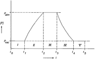
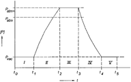
図3aは、装填装置LLのポンプ排気および通気のサイクルにおける装填装置LLの圧力の時間に対するグラフを示す。この場合、例えばウェーハWは、第一および第二環境の間で交換される。このグラフは、5つの部分I,II,III,IV,Vに分けられる。 FIG. 3a shows a graph of loading device LL pressure versus time during the pumping and venting cycle of loading device LL. In this case, for example, the wafer W is exchanged between the first and second environments. This graph is divided into five parts I, II, III, IV and V.
t0〜t1の段階Iの間、装填装置LL内の圧力は実質的にPvac以下である。この段階の間、真空状態に面する第一ドア11は基板W等を装填装置へ、または装填装置から移送するために開くことができる。時刻t1に第一ドア11が閉じられる。t1〜t2の段階IIの間、装填装置LL内の圧力はガス入口13を通して適当なガスを装填装置LLに通気することで実質的にPatmへ回復される。この実施例では、装填装置LLはN2ガスを通気される。ガス入口13はガス供給部17に連結される。時刻t2において、装填装置は実質的に大気圧となり、N2ガスで充満され、大気状態に面する第二ドア12は開くことができる。t2〜t3の段階IIIの間、装填装置LLに対して基板W等を搬出入できる。
During stage I from t 0 to t 1 , the pressure in the loading device LL is substantially less than or equal to P vac . During this phase, the
装填装置LLはN2ガスで充満されるので、第二ドア12が開かれたときに危険粒子や汚損分子が段階IIIの間に装填装置へ流入することはほとんどない。しかしながら幾分かの粒子および/または分子は装填装置LLへ侵入し得る。
Since the loading device LL is filled with N 2 gas, dangerous particles and fouling molecules rarely flow into the loading device during stage III when the
従って、本発明の他の実施例によれば、図3bに見られるように段階IIIの間は過大圧力Patm+が装填装置LL内に形成される。この過大圧力Patm+は、第二ドア12が開かれたときも段階IIIの間にガス入口13を通してN2ガスを流入し続けることによって実現できる。この過大圧力は装填装置LLから大気環境へ向かうガスの流れを生じて、大気環境から装填装置LLへの粒子および/または分子の侵入を最少限に抑える。
Therefore, according to another embodiment of the present invention, an overpressure Patm + is created in the loading device LL during stage III, as seen in FIG. 3b. This overpressure P atm + can be achieved by continuing to flow N 2 gas through the
時刻t3に第二ドア12が閉じられ、また段階IVの間に装填装置LLは実質的にPvac以下になるまでポンプ16によりガス出口15を通してポンプ排気される。装填装置LLからポンプ排気されたガスは、実質的に装填装置LLに供給したガス、すなわちN2ガスである。好ましい実施例では、N2ガスを再使用するために、ガス出口15は例えばフィルタ・システム(図示せず)を経てガス供給部17に連結できる。
At time t 3 the
以上、本発明の具体例について説明したが、本発明は、前記説明以外についても実現できるものである。この説明は、本発明を限定することを意図していない。例えば、本発明は実質的に同圧である第一および第二の環境の間で対象物を移送する方法にも適用されることが理解されるであろう。 As mentioned above, although the specific example of this invention was demonstrated, this invention is realizable also about things other than the said description. This description is not intended to limit the invention. For example, it will be appreciated that the present invention also applies to a method of transferring an object between first and second environments that are substantially at the same pressure.
AM 調整手段
C ターゲット箇所
CO コンデンサ
Ex,IL 放射系
HC 操作室
IN 集積光学装置
LA 放射源
LL 装填装置
MA マスク
MT マスク・テーブル
M1,M2 マスク整合マーク
Patm 大気圧
Patm+ 過大圧力
Pvac 真空圧
PB 放射投影ビーム
PC リトグラフ・パターン形成室
PL 投影系
PM 第一の位置決め手段
PW 第二の位置決め手段
P1,P2 基板整合マーク
W 基板
WT 基板テーブル
1 リトグラフ投影装置
11 第一ドア
12 第二ドア
13 ガス入口
15 ガス出口
16 ポンプ
17 ガス供給部
AM adjustment means C target location CO condenser Ex, IL radiation system HC operation room IN integrated optical device LA radiation source LL loading device MA mask MT mask table M1, M2 mask alignment mark P atm atmospheric pressure P atm + overpressure P vac vacuum pressure PB Radiation projection beam PC Lithographic pattern forming chamber PL Projection system PM First positioning means PW Second positioning means P1, P2 Substrate alignment mark W Substrate WT Substrate table 1
Claims (15)
以下の部材を含むリトグラフ・パターン形成室と、
・所望のパターンに従って投影ビーム(PB)をパターン化する働きをするパターン形成手段(MA)を保持する支持構造(MT)、
・基板(W)を保持する基板テーブル(WT)、および
・パターン化したビームを基板(W)のターゲット箇所に投影する投影系(PL)、
リトグラフ・パターン形成室(PC)から第二の環境に、または、その逆に、対象物(MA,W)を搬送するための装填装置(LL)であり、室を形成し、リトグラフ・パターン形成室に面する第一ドア(11)と、第二の環境に面する第二ドア(12)と、装填装置内を通気するためのガス入口とを含む前記装填装置とを含むリトグラフ投影装置において、
前記ガス入口(13)がガス供給部(17)に連結され、このガス供給部は対象物の搬送の少なくとも一部の間にガス入口(13)にガスを供給し、そのガスには基本的に粒子、酸素、炭化水素およびH2Oの少なくとも一つが含まれていないことを特徴とするリトグラフ投影装置。 A radiation system forming a radiation projection beam (PB);
A lithographic pattern forming chamber including the following members:
A support structure (MT) holding pattern forming means (MA) which serves to pattern the projection beam (PB) according to the desired pattern;
A substrate table (WT) that holds the substrate (W), and a projection system (PL) that projects the patterned beam onto a target location on the substrate (W),
A loading device (LL) for transporting an object (MA, W) from a lithographic pattern forming chamber (PC) to a second environment or vice versa, forming a chamber and forming a lithographic pattern In a lithographic projection apparatus comprising: a first door (11) facing the chamber; a second door (12) facing the second environment; and the loading device including a gas inlet for venting the loading device. ,
The gas inlet (13) is connected to a gas supply part (17), which supplies gas to the gas inlet (13) during at least part of the transport of the object, the gas basically A lithographic projection apparatus characterized in that at least one of particles, oxygen, hydrocarbons and H 2 O is not contained in the lithographic projection apparatus.
放射系を使用して放射投影ビーム(PB)を形成する段階、
投影ビーム(PB)の横断面にパターンを形成するためにパターン形成手段(MA)を使用する段階、
放射線感応材料の層のターゲット箇所(C)に放射投影ビームを投影する段階、および
室を形成し、リトグラフ・パターン形成室(PC)に面する第一ドア(11)と、第二間の環境に面する第二ドア(12)とを含む装填装置(LL)を経て、前記リトグラフ・パターン形成室(PC)に対して基板(W)を搬出入する段階を含むデバイス製造方法において、
搬送の少なくとも一部の間において粒子、酸素、炭化水素およびH2Oの少なくとも一つを事実上含まないガスを装填装置(LL)に通気する段階を含むことを特徴とするデバイス製造方法。 Loading a substrate (W) at least partially covered with a layer of radiation-sensitive material into a lithographic patterning chamber (PC);
Forming a radiation projection beam (PB) using a radiation system;
Using patterning means (MA) to form a pattern in a cross section of the projection beam (PB);
Projecting a radiation projection beam onto a target location (C) of a layer of radiation sensitive material; and a first door (11) forming a chamber and facing a lithographic patterning chamber (PC) and a second environment In a device manufacturing method including a step of carrying a substrate (W) in and out of the lithographic pattern forming chamber (PC) through a loading device (LL) including a second door (12) facing the substrate,
A device manufacturing method comprising: venting a loading device (LL) with a gas that is substantially free of at least one of particles, oxygen, hydrocarbons, and H 2 O during at least a portion of the transfer.
実質的に真空状態(Pvac)以下の圧力となるように装填装置(LL)をポンプ排気する段階、
第一ドア(11)を開く段階、
リトグラフ・パターン形成室(PC)から装填装置(LL)に基板(W)を搬送する段階、
第一ドア(11)を閉成する段階、
実質的に第二圧力(Patm)以上の圧力とするように粒子、酸素、炭化水素およびH2Oの少なくとも一つを事実上含まないガスを装填装置(LL)に通気する段階、
第二ドア(12)を開く段階、および
基板(W)を第二の環境(Patm)へ搬送する段階を含む請求項9に記載されたデバイス製造方法。 Transfer from the lithographic patterning chamber (PC) to the second environment
Pumping the loading device (LL) to a pressure substantially below the vacuum state (P vac );
Opening the first door (11),
Transferring the substrate (W) from the lithographic pattern forming chamber (PC) to the loading device (LL);
Closing the first door (11);
Venting a loading device (LL) with a gas that is substantially free of at least one of particles, oxygen, hydrocarbons, and H 2 O to a pressure substantially equal to or greater than a second pressure (P atm );
10. A device manufacturing method according to claim 9, comprising the steps of opening a second door (12) and transporting the substrate (W) to a second environment (P atm ).
放射系を使用して放射投影ビーム(PB)を形成する段階、
投影ビーム(PB)の横断面にパターンを形成するためにパターン形成手段(MA)を使用する段階、
放射線感応材料の層のターゲット箇所(C)に放射投影ビームを投影する段階、および
室を形成し、リトグラフ・パターン形成室(PC)に面する第一ドア(11)と、第二間の環境に面する第二ドア(12)とを含む装填装置(LL)を経て、前記リトグラフ・パターン形成室(PC)から、および前記リトグラフ・パターン形成室(PC)へ、対象物を搬送する段階を含むデバイス製造方法において、
搬送の少なくとも一部の間において粒子、酸素、炭化水素およびH2Oの少なくとも一つを事実上含まないガスを装填装置(LL)に通気する段階を含むことを特徴とするデバイス製造方法。 Providing in a lithographic patterning chamber (PC) a substrate (W) at least partially covered with a layer of radiation sensitive material;
Forming a radiation projection beam (PB) using a radiation system;
Using patterning means (MA) to form a pattern in a cross section of the projection beam (PB);
Projecting a radiation projection beam onto a target location (C) of a layer of radiation sensitive material; and a first door (11) forming a chamber and facing a lithographic patterning chamber (PC) and a second environment Conveying the object from the lithographic pattern forming chamber (PC) to and into the lithographic pattern forming chamber (PC) via a loading device (LL) including a second door (12) facing In a device manufacturing method including:
A device manufacturing method comprising: venting a loading device (LL) with a gas that is substantially free of at least one of particles, oxygen, hydrocarbons, and H 2 O during at least a portion of the transfer.
Applications Claiming Priority (1)
| Application Number | Priority Date | Filing Date | Title |
|---|---|---|---|
| EP03076498 | 2003-05-19 |
Publications (1)
| Publication Number | Publication Date |
|---|---|
| JP2005051202A true JP2005051202A (en) | 2005-02-24 |
Family
ID=33547676
Family Applications (1)
| Application Number | Title | Priority Date | Filing Date |
|---|---|---|---|
| JP2004147188A Pending JP2005051202A (en) | 2003-05-19 | 2004-05-18 | Lithographic apparatus and method for manufacturing device |
Country Status (6)
| Country | Link |
|---|---|
| US (1) | US20050002003A1 (en) |
| JP (1) | JP2005051202A (en) |
| KR (1) | KR20040100948A (en) |
| CN (1) | CN100565345C (en) |
| SG (1) | SG141228A1 (en) |
| TW (1) | TWI289733B (en) |
Families Citing this family (5)
| Publication number | Priority date | Publication date | Assignee | Title |
|---|---|---|---|---|
| US7151589B2 (en) * | 2004-06-24 | 2006-12-19 | Asml Netherlands B.V. | Lithographic apparatus and patterning device transport |
| US7638385B2 (en) * | 2005-05-02 | 2009-12-29 | Semiconductor Components Industries, Llc | Method of forming a semiconductor device and structure therefor |
| JP4325715B2 (en) * | 2007-09-28 | 2009-09-02 | セイコーエプソン株式会社 | Pattern forming device |
| US10627728B2 (en) * | 2017-06-14 | 2020-04-21 | Taiwan Semiconductor Manufacturing Co., Ltd. | Method for creating vacuum in load lock chamber |
| DE102019117484B4 (en) * | 2019-06-28 | 2021-07-08 | Carl Zeiss Smt Gmbh | Method and arrangement for loading a component into a loading position in an optical system for microlithography |
Family Cites Families (14)
| Publication number | Priority date | Publication date | Assignee | Title |
|---|---|---|---|---|
| US5523193A (en) * | 1988-05-31 | 1996-06-04 | Texas Instruments Incorporated | Method and apparatus for patterning and imaging member |
| DE59105735D1 (en) * | 1990-05-02 | 1995-07-20 | Fraunhofer Ges Forschung | EXPOSURE DEVICE. |
| US5314541A (en) * | 1991-05-28 | 1994-05-24 | Tokyo Electron Limited | Reduced pressure processing system and reduced pressure processing method |
| US5229872A (en) * | 1992-01-21 | 1993-07-20 | Hughes Aircraft Company | Exposure device including an electrically aligned electronic mask for micropatterning |
| US5981399A (en) * | 1995-02-15 | 1999-11-09 | Hitachi, Ltd. | Method and apparatus for fabricating semiconductor devices |
| WO1997033205A1 (en) * | 1996-03-06 | 1997-09-12 | Philips Electronics N.V. | Differential interferometer system and lithographic step-and-scan apparatus provided with such a system |
| US20020104206A1 (en) * | 1996-03-08 | 2002-08-08 | Mitsuhiro Hirano | Substrate processing apparatus |
| US5855681A (en) * | 1996-11-18 | 1999-01-05 | Applied Materials, Inc. | Ultra high throughput wafer vacuum processing system |
| EP0890136B9 (en) * | 1996-12-24 | 2003-12-10 | ASML Netherlands B.V. | Two-dimensionally balanced positioning device with two object holders, and lithographic device provided with such a positioning device |
| US6375746B1 (en) * | 1998-07-10 | 2002-04-23 | Novellus Systems, Inc. | Wafer processing architecture including load locks |
| US6486444B1 (en) * | 1999-06-03 | 2002-11-26 | Applied Materials, Inc. | Load-lock with external staging area |
| SG106599A1 (en) * | 2000-02-01 | 2004-10-29 | Tokyo Electron Ltd | Substrate processing apparatus and substrate processing method |
| US7076920B2 (en) * | 2000-03-22 | 2006-07-18 | Mks Instruments, Inc. | Method of using a combination differential and absolute pressure transducer for controlling a load lock |
| JP4689064B2 (en) * | 2000-03-30 | 2011-05-25 | キヤノン株式会社 | Exposure apparatus and device manufacturing method |
-
2004
- 2004-05-14 SG SG200402613-4A patent/SG141228A1/en unknown
- 2004-05-18 TW TW093114009A patent/TWI289733B/en not_active IP Right Cessation
- 2004-05-18 CN CNB2004100639083A patent/CN100565345C/en not_active Expired - Fee Related
- 2004-05-18 KR KR1020040035063A patent/KR20040100948A/en active Search and Examination
- 2004-05-18 JP JP2004147188A patent/JP2005051202A/en active Pending
- 2004-05-18 US US10/847,656 patent/US20050002003A1/en not_active Abandoned
Also Published As
| Publication number | Publication date |
|---|---|
| TWI289733B (en) | 2007-11-11 |
| CN100565345C (en) | 2009-12-02 |
| US20050002003A1 (en) | 2005-01-06 |
| CN1550890A (en) | 2004-12-01 |
| SG141228A1 (en) | 2008-04-28 |
| KR20040100948A (en) | 2004-12-02 |
| TW200510952A (en) | 2005-03-16 |
Similar Documents
| Publication | Publication Date | Title |
|---|---|---|
| JP4743440B2 (en) | Lithographic projection apparatus and device manufacturing method | |
| JP4021419B2 (en) | Temperature controlled load lock, lithographic apparatus with load lock, and method of manufacturing a substrate using the load lock | |
| JP2006179906A (en) | Lithography device and device manufacturing method | |
| JP2009246375A (en) | Lithographic apparatus and device manufacturing method | |
| JP4035510B2 (en) | Lithographic apparatus including a gas cleaning system | |
| KR100695555B1 (en) | Lithographic apparatus and device manufacturing method | |
| JP2005020009A (en) | Lithography projection equipment and device manufacturing method | |
| JP4073904B2 (en) | Method and apparatus for supplying a dynamic protective layer to a mirror | |
| JP4846583B2 (en) | Adaptive temperature control system for lithography chemical process | |
| US20070188723A1 (en) | Lithographic apparatus and device manufacturing method | |
| JP3836751B2 (en) | Lithographic projection apparatus, element manufacturing method, and element manufactured thereby | |
| JP2005051202A (en) | Lithographic apparatus and method for manufacturing device | |
| JP2003229358A (en) | Lithographic device, device manufacturing method, device manufactured thereby, and computer program | |
| US7230673B2 (en) | Lithographic apparatus, reticle exchange unit and device manufacturing method | |
| JP4339377B2 (en) | Gas laser apparatus and method | |
| JP4048205B2 (en) | Lithographic apparatus and device manufacturing method | |
| US7088421B2 (en) | Lithographic apparatus, device manufacturing method, and device manufactured thereby | |
| JP2004247731A (en) | Lithography apparatus and method of detecting accurate fixing of object | |
| JP4331099B2 (en) | Lithographic apparatus and device manufacturing method | |
| EP1596421A2 (en) | Lithographic apparatus and device manufacturing method | |
| KR20100100921A (en) | A lithographic apparatus, a projection system and a device manufacturing method | |
| EP1396759A2 (en) | Lithographic apparatus, device manufacturing method, and device manufactured thereby | |
| JP2007251133A (en) | Lithographic apparatus and device manufacturing method | |
| JP2005020007A (en) | Sealing assembly, lithography projection apparatus and device manufacturing method |
Legal Events
| Date | Code | Title | Description |
|---|---|---|---|
| RD03 | Notification of appointment of power of attorney |
Free format text: JAPANESE INTERMEDIATE CODE: A7423 Effective date: 20060904 |
|
| RD05 | Notification of revocation of power of attorney |
Free format text: JAPANESE INTERMEDIATE CODE: A7425 Effective date: 20070530 |
|
| A977 | Report on retrieval |
Free format text: JAPANESE INTERMEDIATE CODE: A971007 Effective date: 20070608 |
|
| A131 | Notification of reasons for refusal |
Free format text: JAPANESE INTERMEDIATE CODE: A131 Effective date: 20070615 |
|
| A521 | Written amendment |
Free format text: JAPANESE INTERMEDIATE CODE: A523 Effective date: 20070918 |
|
| A131 | Notification of reasons for refusal |
Free format text: JAPANESE INTERMEDIATE CODE: A131 Effective date: 20080107 |
|
| A521 | Written amendment |
Free format text: JAPANESE INTERMEDIATE CODE: A523 Effective date: 20080402 |
|
| A02 | Decision of refusal |
Free format text: JAPANESE INTERMEDIATE CODE: A02 Effective date: 20080930 |
|
| A521 | Written amendment |
Free format text: JAPANESE INTERMEDIATE CODE: A523 Effective date: 20110126 |