JP2004519666A - Method and apparatus for detecting and measuring accumulation of magnetic particles - Google Patents
Method and apparatus for detecting and measuring accumulation of magnetic particles Download PDFInfo
- Publication number
- JP2004519666A JP2004519666A JP2002566677A JP2002566677A JP2004519666A JP 2004519666 A JP2004519666 A JP 2004519666A JP 2002566677 A JP2002566677 A JP 2002566677A JP 2002566677 A JP2002566677 A JP 2002566677A JP 2004519666 A JP2004519666 A JP 2004519666A
- Authority
- JP
- Japan
- Prior art keywords
- magnetic field
- sensor
- excitation current
- sample
- particles
- Prior art date
- Legal status (The legal status is an assumption and is not a legal conclusion. Google has not performed a legal analysis and makes no representation as to the accuracy of the status listed.)
- Pending
Links
Images


Classifications
-
- G—PHYSICS
- G01—MEASURING; TESTING
- G01N—INVESTIGATING OR ANALYSING MATERIALS BY DETERMINING THEIR CHEMICAL OR PHYSICAL PROPERTIES
- G01N27/00—Investigating or analysing materials by the use of electric, electrochemical, or magnetic means
- G01N27/72—Investigating or analysing materials by the use of electric, electrochemical, or magnetic means by investigating magnetic variables
- G01N27/74—Investigating or analysing materials by the use of electric, electrochemical, or magnetic means by investigating magnetic variables of fluids
- G01N27/745—Investigating or analysing materials by the use of electric, electrochemical, or magnetic means by investigating magnetic variables of fluids for detecting magnetic beads used in biochemical assays
-
- G—PHYSICS
- G01—MEASURING; TESTING
- G01R—MEASURING ELECTRIC VARIABLES; MEASURING MAGNETIC VARIABLES
- G01R33/00—Arrangements or instruments for measuring magnetic variables
- G01R33/12—Measuring magnetic properties of articles or specimens of solids or fluids
- G01R33/1215—Measuring magnetisation; Particular magnetometers therefor
Abstract
Description
【0001】
【技術分野】
本発明は、一般的には磁性粒子の存在の検出に関し、特にDC磁気励起および粒子の磁気モーメントにもたらされた励起の大きさ検出によるこのような粒子の蓄積の定量的測度に関する。
【0002】
【背景技術および発明解決しようとする課題】
分子が存在する混合体あるいは溶液の中でその粒子の存在を確定し、またできれば濃度を測定する技術へ高い関心が寄せられてきた。ある種の有機化合物の極めて低い濃度を測定することは状況によって望ましい。たとえば、医学では生理的流体(例:血液や尿)にもともと存在する、あるいは生物系に導入された(例:薬剤や汚染物質)特定の分子の濃度を通常は溶液中で確定することは非常に有用である。
【0003】
対象である特定の化合物の存在を検出するのに普及している1つの方法は免疫学的検定方法である。この方法では、一般的にリガンドと呼ばれる特定の分子を検出するために、特に対象のリガンドと結合する非リガンドあるいは受容体とも呼ばれる第二の分子種を利用する。リガンドと非リガンドの結合状態を直接的あるいは間接的に測定あるいは推測することにより対象のリガンドの存在を検出する。
【0004】
米国特許第4,537,861号でElings らはいくつかの検出法および測定法を開示している。この特許は、典型的には抗原および抗体であるリガンドと非リガンドとの結合反応の溶液中で同種免疫学的検定を実行するいくつかの方法に関係している。Elingsは固体基板に付着させた非リガンド物質の分離部位の立体配列から成る立体パターンの作成を教示している。特有の物理的特性を有する分子や粒子を取り付けることによってラベル処理された対応リガンドは、標識(labeled)リガンドが立体パターン中で非リガンドと結合反応できるように固体基板に分散させられる。望ましい免疫学的検定は、標識結合複合体の立体パターン中での蓄積後、装置で固体基板をスキャンしてラベルの物理的特性を測定する。このスキャナは蛍光性、光学濃度、光散乱、色および反射率等を利用することができる。さらにElingsによると、磁性粒子は標識結合複合体を溶液中あるいは固体基板上に蓄積させるためにリガンドあるいは標識リガンドに付着させることができ、その後に上記のスキャン技術を利用する。
【0005】
実際、磁鉄鉱と不活性マトリクス材から成る磁性粒子は、生物化学分野で長い間使用されている。磁性粒子のサイズの範囲は直径数ナノメーターから数ミクロンで、15%から100%の磁鉄鉱を含む。これらはよく超常磁性粒子と呼ばれ、サイズが大きいものは磁気ビーズと呼ばれる。通常の手順は、粒子を特定のミクロ物体あるいは対象の粒子(例:蛋白質、ウィルス、細胞、DNA断片)と堅く結合させる生物学的活性物質で粒子表面を塗装する。それにより磁性粒子は“ハンドル”となり、通常は高強度の永久磁石によって提供される磁気傾斜を用いて物体を移動させたり、固定することが可能になる。Elingsの特許は磁性粒子のこのような使用の一例である。希土類磁石および鉄極を使用した特製組立構造物は市販されており、利用可能である。
【0006】
これらの磁性粒子は主として結合物体を移動あるいは固定させるために使用されてきたが、いくつかの実験研究では結合複合体の存在を検出するためのタグとして使用されている。従来の結合複合物の検出と数量化では、対象の複合物に結合した放射能、蛍光あるいはリン光分子を使用してきた。これらの従来のタギング方法はさまざまな重大な弱点を持つ。放射能方法は発生する低レベル放射能廃棄物のもたらす健康面および処理面の問題があり、また処理が比較的遅い。蛍光あるいはリン光方法は、放射される光子がサンプル内の他の物質に吸収されるため量的精度および動的範囲において限定的である。(日本特許公開第63−90765号、1988年4月21日、藤沢ほか)さらに、蛍光あるいはリン光分子からの信号は、通常は数時間から最長数日で崩壊する。
【0007】
一方で、小量の磁性粒子からの信号は極度に小さいため、多くの利用法において最も感度の高い磁界検出器であると考えられている超伝導量子干渉素子(スキッド)に基づく検出器を多くの研究者が開発しようと試みてきたことは当然である。しかしながら、この方法には実質的な難点がいくつか含まれている。スキッドのピックアップループは低温で維持されなければならないため、サンプルはこれらのループと非常に緊密にカップリングするよう冷却されなければならない。これによって測定は許容できないほど長くなり、多くのバイオテクノロジー分野での利用法には不適切である。さらにこの方法はスキッドの通常の複雑性とその関連極低温部品のために非常に高価となり、安価なデスクトップ装置での使用には通常は不適切である。高Tc超伝導体に基づく設計でもこの難点を完全には解決できず、藤沢らにより記述されているように新たないくつかの問題を生じる。
【0008】
より伝統的な磁性粒子の検出および測量方法は、サンプルを強磁気傾斜に置き、サンプル上に発生する強度を測定するという強度磁気測定(force magnetometry)のいくつかの形態を典型的に含んできた。たとえば強度平衡磁気測定では、傾度が変化した際のサンプル重量の外見上の変化として強度を測定する。この方法の一例はロール特許第5,445,970 号および第5,445,971号に開示されている。より複雑な技術は、マイクロマシンカンチレバーの偏向あるいは振動への粒子の影響を測定する(Baselt et al., A Biosensor Based on Force Microscope Technology, NaVal Research Lab., J. Vac. Science Tech. B., Vol14, No.2, 5頁, 1996年4月号参照)。これらの方法は本質的には磁気効果を機械反応に変換することによるため、振動、粘度、および浮力といったその他の機械効果の類と区別しなければならず、対象の測定が実質的に干渉されるために限定的である。
【0009】
米国特許第6,046,585号で、Simmonsはトロイダルマグネタイザーに小領域(隙間部)を提供した技術について記述している。その技術ではその隙間部内に1対(あるいは複数対)の誘導検出コイルが配置され、高周波振動磁場(ドライブ磁場)を発生させる。この場合個別の検出コイルのサイズは厳密に一致しているが巻き方向が反対であるため、その他の磁性体(例:磁気結合複合物に含まれる磁性粒子)の不在下ではコイル対の出力電圧はゼロとなる。すなわち、ドライブ磁場は同強度であるが対極でそれぞれの逆巻きコイルと結合するため、個別のコイルからの電圧は計算上合計ゼロになる。
【0010】
固体基板上の磁性粒子の蓄積が検出コイルに近接した隙間部に置かれると、振動ドライブ磁場は磁性粒子中に対応する振動磁化を形成し、検出コイルにより検出可能になる。Simmonsの特許では粒子蓄積の物理的なサイズは検出コイルの1つのサイズとほぼ等しいため、基板が検出コイル配列を通過した時に蓄積粒子は1コイル中で信号を発する。磁性この意味で粒子の蓄積は検出コイルを通過する時に検出コイル配列の有効バランスを変化させると考えられる。Simmonsによると、蓄積の物理的サイズが検出コイル配列中の個別の1コイルのサイズと一致すれば、いかなる特定の磁性粒子蓄積からでも最大信号を得られる。
【0011】
Simmonsの方法では(典型的には500から1000エルステッドの最大振幅を有する)高周波振動磁場は2つの機能を提供する。第一に、磁性粒子中に大きな磁化を形成し、第二に、振動磁場の高周波特性は磁性粒子の誘導された磁化をドライブ磁場と同周波数で振動させる(典型的には100KHz規模)。誘導検出コイル中に誘導された電圧は検出された信号の周波数に比例するため、誘導検出コイルに高周波ドライブ磁場を利用することにより装置の感度は増加して極めて微量の磁性粒子を検出することができる。
【0012】
Simmonsの開示した発明に関する係属中の特許出願は、基本的な概念をいろいろと応用している。第一に、隙間部の形成において高度な対称性を提供するE状磁気コアの使用について記述している。それによって検出コイルに対する高度なバランスを維持する一方で、大ドライブ磁場を形成することができる。第二にフラックスゲート、巨大磁気抵抗(GMR)、巨大磁気抵抗(CMR)、ならびにホール効果センサーなどの他のセンサーの使用を含む別検出システムが開示されており、上述のセンサーはすべて未だにACドライブ磁場を採用している。
【0013】
Simmonsの記述した検出システムは、磁性粒子の磁化を検出および測定するために磁性粒子を含んだ物質の基本的な磁気の性質を利用している。これに使用されているビーズは典型的には超常磁性と呼ばれ、印加磁場に配置された場合のみ磁性である。より具体的には、外的印加磁場の不在下ではビーズは磁性ではない。すなわちビーズは残留磁気を有していない。事実、バイオテクノロジー分野の利用法で使用されるビーズは、むしろ残留磁気を有さないように設計される。残留磁気を有するビーズは溶液中で塊になり、様々な問題を引き起こすためである。それゆえ、バイオテクノロジー分野で典型的に使用されるビーズの磁化の検出あるいは測定装置は、何れも測定中にビーズに外的磁場が加えられる場合のみ機能できる。この状況はテープやディスクの磁気フィルムが高残留磁気および大保磁磁場を有するように設計される磁気録音に使用される技術と区別されなければならない。(物質の保磁磁場は物質を完全に消磁するために加えられる磁場の値を提供する。)実際、録音での利用では大きな残留磁気は情報を実際に保存する手段である。
【0014】
バイオテクノロジー分野での利用法で典型的に使用される磁性粒子は酸化鉄を含んで成り、典型的にはFe3O4とFe2O3の混合物である。様々なメーカーの粒子の測定からこれらの粒子の飽和磁化はサイズに関わらず常に約300エルステッドであることが判明した。これはこの種のフェライト物質にとって非常に典型的な飽和磁場である。より具体的に述べると、これは500エルステッド未満で粒子により大きな磁場を加えると粒子の磁化はさらに増加し、検出される信号が増加する可能性があることを意味している。しかしながら、飽和磁場を超える磁場ではこの効果は激減され、ゆえに印加磁場でのさらなる増加は粒子の磁化の増加をほとんどあるいは全く提供しない。さらに、ほぼすべての磁気検出装置には周囲磁場に比例して増加する雑音源が存在する。それゆえ、飽和レベル以上に印加磁場を増やすことは、その信号対雑音比を減少させることにより測定の質を実際に下げる。また印加磁場での増加によって強磁性汚染物質からの信号への不都合な影響がより明白化する可能性もある。それゆえ、磁化を測定することによって存在する粒子の数量を確定したい場合は、通常は粒子の飽和磁場とほぼ等しい磁場を加えることでこのような測定への信号対雑音比を最良化できる。磁場は我々の場合は500エルステッドである。
【0015】
上記のようにSimmonsの特許は粒子に大振動磁場を加え、また粒子内に誘導された振動磁化を検出することによって結合複合物中の超常磁気粒子の定量的測度を行う技術を記述している。ここで使用されるセンサーは大振動磁場の存在下で良的に機能するタイプのものでなければならない。Simmonsの装置は感度が非常に高く、非常に良く機能する。しかしながらSimmonsの設計をさらに複雑化する要因がいくつかある。最も重要なことに、Simmonsの検出システムは高周波(典型的には100KHz)において機能するため、サンプル/基板の組み合わせと検出コイルとの間に静電結合効果が発生する。さらに、そのような高周波システムは常に印加ACドライブ磁場と検出された信号との間の位相シフトに影響される。このような検出システムを100KHzで操作する場合にはこれらの影響は多大であり、システムが粒子の磁化を正確に測定するためには対処されなければならない。さらに、トロイダルマグネタイザーの隙間部に高周波AC磁場を発生させるには大量の電力を必要とするが、検出器内の熱ドリフトを引き起こす可能性が特に装置が始めに加圧された直後に発生する。ACドライブ磁場が高電力を必要とするため、この種のシステムが電池で作動する時には作動時間の長さも制限される。最終的に、磁石およびコイル内のACドライブは防止すべきRF排出を発生させる可能性がある。
【0016】
【課題を解決するための手段】
本発明は磁性粒子(例:磁鉄鉱)の微小な蓄積および対象の結合複合物を直接的に検出および測定する非常に単純化された安価な方法および装置を提供する。
【0017】
本発明の主眼点は、磁性粒子中に磁化を誘導するために(従来技術の時間的に変化するドライブ磁場に代わる)DC磁場を使用し、それをホールセンサーと組み合わせて誘導された磁化を検出することである。経時変化する磁場の代わりにDC磁場を使用することの利点は大きい。
【0018】
本発明においてDC磁場を発生させるには磁場発生源は必要なく、従来技術のAC被駆動システムに比べて非常に単純であり、部品のコストを約2桁引き下げることができる。必要なDC磁場は、電力を消費せずに、適切な磁場特性を提供する安価な永久磁石と単数あるいは複数の鉄片を用いて発生させることができる。プロトタイプではDC磁場を発生させるために使用される部品は約25セント未満であった。それに比べて既存の装置に使用されている高周波AC磁場を発生させるための部品は20ドルを超え、その上多大な電力を要する。
【0019】
また、100KHzのAC磁場を発生させるために必要な電力は隙間部の容積に従って増加するため、ACドライブ磁場を用いた装置内の測定領域(隙間部)の容積を限定する。隙間部の高さに対する領域比を増加させることにより隙間部内の磁場均一性は高められるが、そのためにACドライブ磁場を使用するシステムでは電力消費が増加するという欠点がある。DC磁場を使用した場合では、隙間部の容積を増加する時にはそれに対応したさらに大きな永久磁石の使用のみが必要である。プロトタイプシステムは隙間部内でSimmonsのACシステムでの容積を倍以上上回る1000エルステッド規模の磁場を達成した。
【0020】
これらの測定を最適化するのに必要とされるやや大きな磁場(500エルステッド規模)は、いくつかのタイプのセンサーと互換性がない。しかしながら、強磁界においてホールセンサーの感度はほとんど落ちない。実際に、センサーはこの規模の磁場で最適に機能するように設計できる。また測定感度を最大限にするために、センサー領域をサンプルのサイズに一致させるべきである。GMRやCMRを含む別タイプのホールセンサーを上記の基準に準拠するように設計することができるが、基準に準ずるホールセンサーは市販されており、安価である。
【0021】
この種の技術に使用される典型的なホールセンサーは、約10から20ミリアンペアの電流が流される。センサーの出力電圧は印加磁場とバイアス電流の両方に比例する。ゆえにバイアス電流の変動は対応する出力信号中の変動を引き起こすため、非常に安定したDC電流を形成するのは難しいだろう。しかしながら、典型的には数キロヘルツでホールセンサーにAC電流を流すことより非常に安定したピーク振幅が発生するので、この問題は容易に対処できる。この方法でホールセンサーにバイアスをかけることによりこの検出システムは数キロヘルツで機能することもでき、達成可能信号対雑音レベルを大幅に高めるために位相検出システムを有効利用できる。(しかしながら、AC電流は本発明に必要ではない。この場合は、センサーにバイアス電流を供給する電子回路の安定性にさらに強い必要性が存在する。)
DC磁場を使用した検出システムはまた、サンプルとセンサーとの間の静電効果に対して非常に免疫性が高い。Simmonsの高周波ACシステムでは、サンプル基板中の誘電特性は誘導性検出コイルの大きな静電結合を引き起こし、見せかけの信号を発生させる可能性もある。適切な位相検出スキームを使用してこれらを拒絶できるが、ホールセンサーを用いたDCシステムはAC静電結合効果への抵抗性が高い。
【0022】
この好適実施例では2体の個別のホール効果センサーは並んで印加磁場に配置され、対応センサー対を形成する。センサーはそれぞれ検出した磁場を示す信号を発生する。一方のセンサーからの信号は他方から減算され、一方のセンサーで他方のセンサー中の信号に対するその一方のセンサーの磁場の差を示す信号を形成する。これらの信号を電子的に減算することにより印加磁場のもたらす不適切な信号を激減させる。そのようなセンサーの構成は、地磁気検出産業ではグラジオメーターと呼ばれている。
【0023】
この測定は、粒子がDC磁場に同時に露出される時に、磁気に影響される粒子の定義されたパターンをホールセンサーに通過および接近させて実行する。Simmonsの従来技術によると、磁性粒子パターンの空間規模をホールセンサーの物理的規模にほぼ一致させることは重要である。この場合、磁性粒子のパターンは通過の際に第一ホールセンサーによって検出され、第一センサーの検出領域から離れた後に引き続き第二ホールセンサーに検出される。2体のホールセンサーは対極性の信号を発生するように接続されているため、2体のセンサー間の差信号は2体のセンサーを通過する際の立体パターンの位置の関数であり、存在する粒子の数量を表す。
【0024】
【発明を実施するための最良の形態】
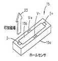
以下の詳細な説明では図面を利用して本発明の目的、特徴および利点をより明確に説明してゆく。図1は本発明による装置10を示している。永久磁石構造体11は中脚部分13、14の間に形成される隙間部12を含んだE状構造を持つ。磁石は磁石要素11a、11bと鉄柱片11c,11dを含んでいる。ホールセンサー15,16は面17に搭載される。この面はホールセンサーとそれらが尾部18のリード線によって接続されている回路との間に必要なすべての外部接続を提供する柔軟なプリント基板でもよい。
【0025】
サンプル21は基板22の定義されたパターン(通常は1ミリx2ミリ)中に配置され、隙間部12内にホールセンサー15,16を通って移動され、後述のようにたとえば図4の回路から出力信号を提供する。この動作とセンサー出力は後に図7と図8を利用してさらに詳述される。
【0026】
別形態として、基板22は上面にバーコード19のプリントされている延長部20を有することができる。バーコードは光学検出器か、あるいは適切な導線29とともに図示されているバーコードリーダー28に読みとられる。バーコードはサンプルパターン21から所定の間隔をおいて配置され、リーダー28はホールセンサーに対する固定位置を有する。そのためリーダーからの信号は、ホールセンサーに対するサンプルパターンの位置情報を提供できる。
【0027】
光学検出器はかなり精密な装置であり、1本のバーコード線が検出器を通過する度に2パルスを発する。第一パルスはバーコード線の最前線に対応し、第二パルスは(方形)バーコード線の最後線に対応する。ここではこれらのパルスは2体のホールセンサーの電圧出力を測定および保存するデータ収集電子機器を作動させるために使われる。またAC電流がホールセンサーにバイアスをかけるのに使われた場合に電流逆流を制御するために使用される。これに似た方法で、光学検波器(または第二光学検波器)からのパルスはデータ収集プロセスを作動および終了させるために利用できる。ゆえに、バーコード情報は電子制御システムにデータ収集を開始あるいは終了する時を知らせ、またサンプルが通過する時のホールセンサーからの信号の各測定に対する位置情報を提供する。
【0028】
図2はホールセンサーの作動原理を示している。低周波ACはホールセンサー15をバイアスあるいは励磁するためにI+あるいはI−で加えられ、センサーの
検出領域15bは基板15a上にある。後にさらに詳述されるように、図4と図5の回路には出力電圧V+およびV−が加えられる。磁石11からの印加磁場は矢印23で示されている。
【0029】
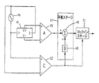
図4の回路は図1の実施例に関する。この好適実施例は低周波交流24に励磁されるホールセンサー対を有する。センサー対からの出力電圧信号は、増幅器25,26によって高インピーダンス法で検出される。続いて回路は2体のセンサー信号の合計と差を表す信号を発生する。センサー近隣での磁性サンプルの不在下で平衡ステージ27の出力信号を最小化するために要素30を用いて平衡増幅率を調節することで、ステージはさらなる信号処理を行う。次に平衡ステージからの利得信号はロックインステージ31への信号入力として利用される。ロックインステージへの基準入力は、好適には信号増幅器32を介して励振源24から同期的にカップリングされる。ロックインステージの出力は存在する粒子物質の量を示す。適切な出力はロックインステージに同期的にカップリングされた励振源を使用しない別方法でも得ることができる。
【0030】
ロックインステージはロックイン技術による信号処理に使用される。この技術は一般的であり、信号処理技術では“位相弁別検出”、“ミキシング”、あるいは“ヘテロダイニング”とも呼ばれる。それは2つの出力と1つの入力を持つ信号処理ステージとして記述されている。この技術は測定装置をAC信号で励磁させ、交流励起と同期の出力信号を検索する。この技術は検出装置に存在する信号雑音および干渉を拒絶する。図4の実施例では、交流励起手段24はホールセンサーを励磁する電流である。励起信号と同期の信号は当該分野では広く認識され、また前述されたように、ロックイン信号処理ステージへの基準入力信号として使用される。センサーからの差信号は、ロックインステージへの別の入力として形成される。この差信号はオプションとして、上記平衡ステージにより調節される。ここで記述されている装置の場合は、ロックインステージの出力信号は存在する粒子物質21の量を示す。センサー雑音と干渉が最小化される周波数スペースの領域で信号検出が実行されるような励起周波数を選択することが望ましい。励起周波数の倍数である周波数で検出することもまた望ましい。
【0031】
上記の信号処理は、能動的および受動的アナログ電子機器、デジタル信号処理、あるいはこれらの併用を含む多くの利用可能な手段によって原則的には実行できる。またアナログ・デジタル変換器、デジタル・アナログ変換器、あるいはその両方を含んでよい。
【0032】
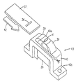
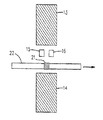
測定するサンプルを図1のような非常に狭い隙間部を通過させるための必要条件はいくつかの利用法では不可能だろう。たとえば、サンプルパターンが非常に厚い基板あるいは体積の大きな物質の表面上に置かれた時に、そのような固体表面を非常に小さな隙間部に通すことは不可能であろう。この種の利用法では必須DC磁場は図3のような構成によって発生させることができる。この構成では鋭く加工された鉄柱先端はDC磁場をホールセンサーの背側から発生させる。このいわゆる片面磁石構造により、より大きくて厚い基板が使用できるが、ホールセンサー(およびサンプル)の位置における磁場が不均一となる不利点も提供される。そのため装置の口径測定は困難になり、定量的測度の精度を低下させ得る。たとえば、不均一な磁場のために測定はサンプルとセンサーの分離に大きく影響されることになり、そのためサンプルの小さな位置変動は測定の不確実性を高める。しかしながら、図3の装置の出力は、図1の実施例が使用できず粒子数の正しい予測が必要な場合には有用である。
【0033】
図3の装置でこの測定を実行するには、基板37上の磁気感応粒子36の定義されたパターンを矢印42の方向でセンサー41の近隣に移動させ、同時に永久磁石構造体43の印加磁場の近隣に移動させる。磁石構造体43は永久磁石38と鋭い形の柱片39を含み、それらは搭載装置40により互いに固定されている。搭載装置はプラスチックのごとき非導電性素材でよい。ホールセンサー41を搭載する面を提供するために、柱片39と磁石38の間の空間はプラスチック40aで充填できる。分離したプラスチック要素でも良いし、搭載装置40と一体構造でも良い。搭載装置40は面40aに固定できるように提供され、固定を補助するために孔部40bが提供される。パターン化粒子とセンサー間との距離の関数としての結果の信号は、サンプル粒子が存在していない時の信号と比較して粒子物質36の量を示す。
【0034】
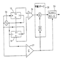
図5は図3の実施例の回路図である。ここではホールセンサー41は低周波交流電流44で励磁される。センサーからの出力電圧信号は、増幅器45によって高インピーダンス法で検出される。励起に比例する信号は46にてセンサーの電圧を示すこの信号と合計される。センサー近隣で磁性サンプルが存在しない場合、平衡ステージ47の出力信号を最小化するために、このステージで平衡化装置48によって平衡増幅率を調整することによって信号は平衡化される。続いてこの結果の合計信号は、上記の好適グラジオメーター実施例で記述された方法と同様に、増幅器52を通る励起信号と同期の基準信号を利用してロックインステージ51で検出される。ロックインステージの出力は存在する粒子物質36の量を示す。
【0035】
図6は本発明はホールセンサーにバイアスをかける2つの方法を規定していることを示す。図4ではホールセンサー15,16は直列接続されているため、両方に同じバイアス電流が流れている。バイアス電流のいかなる変動によっても出力電圧での変化が生じるため、一方のセンサーで変化があった場合にはその変化は他方のセンサーからの(異符号の)同一の変化によって正確に相殺される。しかしながら、それぞれのホールセンサーの長さに沿った大きな電圧降下も存在するため、2体のホールセンサーでV+とラベルされている電圧点はむしろ異なる電位差である。これで第一センサーのV −接続を第二センサーのV+接続に単純に接続することが防止される。(これらの2点を結合させると、バイアス電流の短絡電流経路が第一センサーのV−点から第二電流のV+点まで効果的に形成される。)図4に示すように、それぞれのホールセンサーに分離した差動増幅器25,26を取り付けて使用することで、この問題を避けることができる。またACバイアス電流を使用する場合に2体のセンサー間の電圧差が大きい場合は、両センサー上の電圧点での電位はかなり大きな電位間で急速に切り換わるため不利でもある。
【0036】
図6は別の構成を示しており、ここでは2体のホールセンサー15,16へのバイアス電流55は並列接続されている。この構成は一つのセンサーを通過するバイアス電流中の変動に起因する誤信号の影響をさらに受けやすい。それはこのような変動は他方のセンサーの類似変動に必ずしも正確に一致しないためである。しかしながら、この構成では2体のセンサーのV+点およびV−点での電位はすべてがほぼ同じ電圧である。実際、センサーが完全に一致していると仮定するなら、(ホール電圧がゼロであるような)磁場の不在下では2体のセンサーの4電圧タップは完全に同様の電圧になるだろう。ゆえに、この構成では2体のホールセンサーの電圧タップは互いに接続され、一体の差動増幅器56を用いて2センサーのホール電圧の差が検出される。増幅器57、平衡ステージ58およびロックインステージ59を通過する基準入力は前記同様に機能する。
【0037】
これらの2構成はどちらもその他の測定システムの特定構造次第で好適実施例になりうる。たとえば、AC電流バイアスを使用する際には並列接続バイアススキームは好適であり、センサーが直列に配線されたACバイアスを用いる場合の大きな電圧の揺れを除去することができる。
【0038】
反対に、DC電流バイアスを使用する場合には直列接続バイアススキームはより望ましい。どのような場合でも、直列接続/並列接続、AC/DCのどのような組み合わせでも強調されるべき特徴に応じて利用できる。
【0039】
図7と図8はセンサー反応およびサンプルとセンサーの相対動作のさらなる詳細を示す。磁気信号を背景から区別ができるものとするために、電子センサー信号を録音している間にサンプルをセンサーに対して移動させることは有利である。これは図7に示されている。単数あるいは複数のセンサー15,16上にサンプル21が移動すると、サンプルの磁束はセンサー内にカップリングする。位置関数として録音されるセンサー信号(図8)は、サンプルパターンの形状およびセンサーの空間反応を示す。図1のようにグラジオメーター構造に2体のセンサーが含まれる場合、サンプルは一方のセンサーに近接した時に一極の信号を発生させ、他方のセンサーに近接した時に対極の信号を発生させる。
【0040】
図8はサンプル位置に対して座標で示された測定値集合を示す。実線曲線は最小二乗法を用いて理想的反応関数に適合した曲線を示している。位置および信号電圧の情報を両方使用して、サンプルの磁気モーメントの完全な計算値を導くことができることは明白である。これは磁気背景のレベルから独立的であり、信号電圧のいかなる電子的ずれあるいは不均衡のずれからも独立的である。
【0041】
好適には、鉄柱片は鉄製であるが、高透磁率を有する必要がある。それらはコバルト、ニッケルあるいは必要な特性を有する適切な合金で提供できる。柱片はカーブさせて、隙間部12のような隙間部を正面にすることができる。図1のように2つの磁石ではなく、ひとつのC型磁石を使用できる。基板22は対象領域21を持った横方向フロー膜でよい。好適には、基板は非導電性であって非電磁素材により構成され、プラスチック、木材、あるいは上記の必要条件を満たすその他の素材で構成できる。基材22は手動でセンサーを通過させることができる。あるいはステッピングモーター、サーボモーター、あるいはサンプルをセンサーに対して移動させることのできる別手段を用いて動作を機械化しても良い。本発明にとって動作方法は決定的ではない。
【0042】
本発明のシステムは、1ナノボルトから10ミクロボルトの範囲で優れた感度を持つ。すなわち、本発明は大きな磁場(500〜1000エルステッド)の存在下で極小信号を検出する高感度磁性センサーに利用できる。検出された信号は対象の粒子の存在に起因する磁場中の変化であり、変化はミリエルステッド規模である。ここで有効な等式は、
V=IB/end
である。
式中のVは検出された電圧変動、
Iはバイアス電流、
nはキャリヤ密度、。
Bは印加磁場、
dは検出面の厚み、
eはキャリヤ電荷。
【0043】
変更や改善が当業者によって発明の範囲内で加えられることは明白である。したがって本発明は「請求の範囲」およびその均等物によってのみ限定される。
【図面の簡単な説明】
【図1】図1は本発明の装置の好適実施例の斜視図である。
【図2】図2は図1の実施例に使用されているホールセンサーを示している。
【図3】図3は本発明の別実施例の斜視図である。
【図4】図4は図1の実施例で利用可能な例示回路のブロック図である。
【図5】図5は図3の実施例で利用可能な例示回路のブロック図である。
【図6】図6は図1のホールセンサーをバイアスさせる別方法を組み込んだブロック図である。
【図7】図7は図1のセンサーに対するサンプルの動きを示す概略断面図である。
【図8】図8は図7に示される動作に従うセンサー出力の曲線グラフである。[0001]
【Technical field】
The present invention relates generally to the detection of the presence of magnetic particles, and more particularly to DC magnetic excitation and a quantitative measure of the accumulation of such particles by detecting the magnitude of the excitation imparted to the magnetic moment of the particles.
[0002]
BACKGROUND ART AND PROBLEMS TO BE SOLVED
There has been a great deal of interest in techniques for determining the presence of, and preferably for determining the concentration of, particles in a mixture or solution in which the molecules are present. It may be desirable in some situations to measure very low concentrations of certain organic compounds. For example, in medicine it is very difficult to determine the concentration of certain molecules that are naturally present in physiological fluids (eg, blood or urine) or introduced into biological systems (eg, drugs or contaminants), usually in solution. Useful for
[0003]
One popular method for detecting the presence of a particular compound of interest is an immunoassay. This method utilizes a second molecular species, also called a non-ligand or receptor, that specifically binds the ligand of interest to detect a particular molecule, commonly called a ligand. The presence or absence of the target ligand is detected by directly or indirectly measuring or estimating the binding state between the ligand and the non-ligand.
[0004]
Elings et al. In U.S. Pat. No. 4,537,861 disclose several detection and measurement methods. This patent relates to several methods of performing alloimmunological assays in solution of the binding reaction of a ligand with a non-ligand, typically antigens and antibodies. Elings teaches the creation of a three-dimensional pattern consisting of a three-dimensional array of separation sites for non-ligand material attached to a solid substrate. The corresponding ligand, which has been labeled by attaching molecules or particles with unique physical properties, is dispersed on a solid substrate so that the labeled ligand can react with the non-ligand in a steric pattern. A preferred immunoassay measures the physical properties of the label by scanning the solid substrate with an instrument after accumulation of the label binding complex in a three-dimensional pattern. This scanner can utilize fluorescence, optical density, light scattering, color and reflectivity, and the like. Further, according to Elings, magnetic particles can be attached to a ligand or labeled ligand to allow the labeled binding complex to accumulate in solution or on a solid substrate, and then utilize the scanning techniques described above.
[0005]
In fact, magnetic particles composed of magnetite and an inert matrix material have long been used in the field of biochemistry. Magnetic particles range in size from a few nanometers to a few microns in diameter and contain 15% to 100% magnetite. These are often called superparamagnetic particles, and those with a large size are called magnetic beads. The usual procedure is to coat the particle surface with a biologically active substance that tightly binds the particle to a particular micro-object or particle of interest (eg, proteins, viruses, cells, DNA fragments). The magnetic particles then become "handles" and allow the object to be moved or fixed using a magnetic gradient, usually provided by a high strength permanent magnet. The Elings patent is an example of such a use of magnetic particles. Specially assembled structures using rare earth magnets and iron poles are commercially available and available.
[0006]
Although these magnetic particles have been used primarily to move or immobilize binding entities, some experimental studies have used them as tags to detect the presence of binding complexes. Conventional detection and quantification of bound complexes have used radioactive, fluorescent or phosphorescent molecules bound to the complex of interest. These conventional tagging methods have various significant weaknesses. Radioactive methods suffer from health and processing problems caused by the low level radioactive waste generated and are relatively slow to process. Fluorescence or phosphorescence methods are limited in quantitative accuracy and dynamic range because the emitted photons are absorbed by other substances in the sample. (Japanese Patent Publication No. 63-90765, Apr. 21, 1988, Fujisawa et al.) Furthermore, signals from fluorescent or phosphorescent molecules usually decay in hours to days.
[0007]
On the other hand, since the signal from a small amount of magnetic particles is extremely small, many detectors based on superconducting quantum interference devices (skids) are considered to be the most sensitive magnetic field detectors in many applications. Not surprisingly, some researchers have tried to develop it. However, this method has some substantial difficulties. Since the skid pickup loops must be maintained at a low temperature, the sample must be cooled to couple very tightly with these loops. This makes the measurement unacceptably long and unsuitable for use in many biotechnology applications. Moreover, this method is very expensive due to the usual complexity of skids and their associated cryogenic components, and is usually unsuitable for use in inexpensive desktop devices. Even designs based on high Tc superconductors cannot completely solve this difficulty, and create some new problems as described by Fujisawa et al.
[0008]
More traditional methods of magnetic particle detection and surveying have typically included some form of force magnetometry in which a sample is placed on a strong magnetic gradient and the intensity generated on the sample is measured. . For example, in the intensity equilibrium magnetic measurement, the intensity is measured as an apparent change in the sample weight when the inclination changes. One example of this method is disclosed in Roll Patent Nos. 5,445,970 and 5,445,971. A more complex technique measures the effect of particles on the deflection or vibration of a micromachined cantilever (Baselt et al., A Biosensor Based on Force Microscope Technology, NaVal Research Lab., J. Vec. , No. 2, page 5, April 1996). Because these methods essentially rely on converting magnetic effects into mechanical reactions, they must be distinguished from other types of mechanical effects such as vibration, viscosity, and buoyancy, and the measurement of the object is substantially interfered with. To be limited.
[0009]
In U.S. Patent No. 6,046,585, Simmons describes a technique that provided a small area (gap) to a toroidal magnetizer. In that technique, a pair (or a plurality of pairs) of inductive detection coils are arranged in the gap to generate a high-frequency oscillating magnetic field (drive magnetic field). In this case, the sizes of the individual detection coils are exactly the same, but the winding directions are opposite, so that the output voltage of the coil pair in the absence of other magnetic substances (eg, magnetic particles contained in the magnetic coupling composite). Becomes zero. That is, since the drive magnetic field has the same strength but is coupled to each counter-wound coil at the opposite pole, the voltages from the individual coils are calculated to total zero.
[0010]
When the accumulation of magnetic particles on the solid substrate is placed in the gap adjacent to the detection coil, the oscillating drive magnetic field forms a corresponding oscillating magnetization in the magnetic particles, which can be detected by the detection coil. In Simmons, since the physical size of the particle accumulation is approximately equal to the size of one of the detection coils, the accumulation particles emit a signal in one coil as the substrate passes through the detection coil array. Magnetism In this sense, the accumulation of particles is thought to change the effective balance of the detector coil array as it passes through the detector coil. According to Simmons, the maximum signal can be obtained from any particular magnetic particle accumulation if the physical size of the accumulation matches the size of one individual coil in the sensing coil array.
[0011]
In the Simmons method, a high frequency oscillating magnetic field (typically having a maximum amplitude of 500 to 1000 Oe) provides two functions. First, a large magnetization is formed in the magnetic particles, and second, the high frequency characteristics of the oscillating magnetic field cause the induced magnetization of the magnetic particles to oscillate at the same frequency as the drive magnetic field (typically on the order of 100 KHz). Since the voltage induced in the induction detection coil is proportional to the frequency of the detected signal, the use of a high-frequency drive magnetic field in the induction detection coil increases the sensitivity of the device to detect very small amounts of magnetic particles. it can.
[0012]
Pending patent applications relating to the invention disclosed by Simmons apply various basic concepts. First, the use of an E-shaped magnetic core that provides a high degree of symmetry in the formation of the gap is described. Thereby, a high drive magnetic field can be formed while maintaining a high balance for the detection coil. Secondly, alternative detection systems have been disclosed, including the use of fluxgates, giant magnetoresistance (GMR), giant magnetoresistance (CMR), and other sensors such as Hall effect sensors, all of which are still AC-driven. Uses a magnetic field.
[0013]
The detection system described by Simmons utilizes the basic magnetic properties of the material containing the magnetic particles to detect and measure the magnetization of the magnetic particles. The beads used for this are typically called superparamagnetic and are only magnetic when placed in an applied magnetic field. More specifically, the beads are not magnetic in the absence of an externally applied magnetic field. That is, the beads have no remanence. In fact, beads used in applications in the biotechnology field are rather designed to have no remanence. This is because beads having remanent magnetism clump in a solution and cause various problems. Therefore, any device for detecting or measuring the magnetization of beads, which is typically used in the field of biotechnology, can only work if an external magnetic field is applied to the beads during the measurement. This situation must be distinguished from the technology used for magnetic recording in which magnetic films on tapes and disks are designed to have high remanence and coercivity. (The coercive field of a material provides the value of the magnetic field applied to completely demagnetize the material.) In fact, in recording applications, large remanence is a means of actually storing information.
[0014]
Magnetic particles typically used in applications in the biotechnology field comprise iron oxide, typically Fe 3 O 4 And Fe 2 O 3 Is a mixture of Measurements of particles from various manufacturers have shown that the saturation magnetization of these particles is always about 300 Oersted regardless of size. This is a very typical saturation field for this type of ferrite material. More specifically, this means that applying a larger magnetic field to the particle below 500 Oe will further increase the magnetization of the particle and may increase the detected signal. However, at magnetic fields above the saturation field, this effect is severely diminished, so that further increases in the applied magnetic field provide little or no increase in the magnetization of the particles. In addition, almost all magnetic sensing devices have noise sources that increase in proportion to the ambient magnetic field. Therefore, increasing the applied magnetic field above the saturation level actually reduces the quality of the measurement by reducing its signal-to-noise ratio. The adverse effect on the signal from ferromagnetic contaminants may also become more apparent with an increase in the applied magnetic field. Therefore, if one wants to determine the number of particles present by measuring the magnetization, the signal-to-noise ratio for such measurements can usually be optimized by applying a magnetic field that is approximately equal to the saturation field of the particles. The magnetic field is 500 Oersted in our case.
[0015]
As described above, Simmons describes a technique for applying a large oscillating magnetic field to a particle and detecting the oscillating magnetization induced in the particle to provide a quantitative measure of superparamagnetic particles in a bound composite. . The sensors used here must be of a type that performs well in the presence of large oscillating magnetic fields. The Simmons device is very sensitive and works very well. However, there are several factors that further complicate Simmons' design. Most importantly, the Simmons detection system works at high frequencies (typically 100 KHz), creating an electrostatic coupling effect between the sample / substrate combination and the detection coil. Further, such high frequency systems are always subject to a phase shift between the applied AC drive field and the detected signal. These effects are significant when operating such a detection system at 100 KHz and must be addressed for the system to accurately measure the magnetization of the particles. Furthermore, generating a high-frequency AC magnetic field in the gap of the toroidal magnetizer requires a large amount of power, but the possibility of causing thermal drift in the detector occurs especially immediately after the device is first pressurized. . Due to the high power requirements of the AC drive magnetic field, the length of time that this type of system runs on batteries is also limited. Eventually, AC drives in magnets and coils can generate RF emissions that should be prevented.
[0016]
[Means for Solving the Problems]
The present invention provides a very simplified and inexpensive method and apparatus for directly detecting and measuring minute accumulations of magnetic particles (eg, magnetite) and binding complexes of interest.
[0017]
The focus of the present invention is to use a DC magnetic field (instead of the time-varying drive field of the prior art) to induce magnetization in magnetic particles and combine it with a Hall sensor to detect the induced magnetization. It is to be. The advantages of using a DC magnetic field instead of a time-varying magnetic field are significant.
[0018]
Generating a DC magnetic field in the present invention does not require a magnetic field source, is much simpler than prior art AC driven systems, and can reduce component costs by about two orders of magnitude. The required DC magnetic field can be generated without power consumption using inexpensive permanent magnets and one or more iron pieces that provide the appropriate magnetic field characteristics. In the prototype, the components used to generate the DC magnetic field were less than about 25 cents. In comparison, the components used to generate high-frequency AC magnetic fields used in existing devices are in excess of $ 20 and require significant power.
[0019]
Further, since the power required to generate an AC magnetic field of 100 KHz increases in accordance with the volume of the gap, the volume of the measurement region (gap) in the apparatus using the AC drive magnetic field is limited. Increasing the area ratio to the height of the gap increases the magnetic field uniformity in the gap, but has the disadvantage of increasing power consumption in systems using AC drive magnetic fields. When a DC magnetic field is used, when the volume of the gap is increased, it is only necessary to use a correspondingly larger permanent magnet. The prototype system achieved a magnetic field on the order of 1000 Oersteds in the gap more than double the volume of the Simmons AC system.
[0020]
The rather large magnetic fields (500 Oersted scale) required to optimize these measurements are not compatible with some types of sensors. However, the sensitivity of the Hall sensor hardly decreases in a strong magnetic field. In fact, sensors can be designed to work optimally with magnetic fields of this magnitude. Also, the sensor area should be matched to the size of the sample to maximize the measurement sensitivity. Other types of Hall sensors, including GMR and CMR, can be designed to comply with the above criteria, but Hall sensors that meet the criteria are commercially available and inexpensive.
[0021]
A typical Hall sensor used in this type of technology draws about 10 to 20 milliamps. The output voltage of the sensor is proportional to both the applied magnetic field and the bias current. Therefore, it will be difficult to form a very stable DC current, since variations in the bias current will cause variations in the corresponding output signal. However, this problem can be easily addressed because passing a current through the Hall sensor at typically several kilohertz produces a much more stable peak amplitude. By biasing the Hall sensor in this manner, the detection system can also function at several kilohertz, and the phase detection system can be exploited to significantly increase the achievable signal to noise level. (However, AC current is not required for the present invention, in which case there is a greater need for stability in the electronics that provide the bias current to the sensor.)
Detection systems using DC magnetic fields are also very immune to electrostatic effects between the sample and the sensor. In Simmons' high frequency AC systems, the dielectric properties in the sample substrate can cause large capacitive coupling of the inductive sensing coil, which can also generate spurious signals. These can be rejected using appropriate phase detection schemes, but DC systems with Hall sensors are more resistant to AC capacitive coupling effects.
[0022]
In this preferred embodiment, two individual Hall effect sensors are placed side by side in the applied magnetic field to form a corresponding sensor pair. The sensors each generate a signal indicating the detected magnetic field. The signal from one sensor is subtracted from the other to form a signal at one sensor that indicates the difference in the magnetic field of that one sensor with respect to the signal in the other sensor. By electronically subtracting these signals, inappropriate signals caused by the applied magnetic field are drastically reduced. Such a sensor configuration is called a gradiometer in the geomagnetic detection industry.
[0023]
This measurement is performed by passing and approaching a defined pattern of magnetically affected particles to a Hall sensor when the particles are simultaneously exposed to a DC magnetic field. According to Simmons' prior art, it is important to make the spatial scale of the magnetic particle pattern approximately match the physical scale of the Hall sensor. In this case, the pattern of the magnetic particles is detected by the first Hall sensor during the passage, and is subsequently detected by the second Hall sensor after leaving the detection area of the first sensor. Since the two Hall sensors are connected to generate opposite polarity signals, the difference signal between the two sensors is a function of the position of the three-dimensional pattern as it passes through the two sensors and exists. Indicates the number of particles.
[0024]
BEST MODE FOR CARRYING OUT THE INVENTION
In the following detailed description, objects, features and advantages of the present invention will be more clearly described with reference to the drawings. FIG. 1 shows a
[0025]
The
[0026]
Alternatively, the
[0027]
Optical detectors are fairly precise devices, emitting two pulses each time a bar code line passes through the detector. The first pulse corresponds to the front line of the bar code line, and the second pulse corresponds to the last line of the (square) bar code line. Here, these pulses are used to activate data acquisition electronics that measure and store the voltage output of the two Hall sensors. Also used to control current backflow when AC current is used to bias the Hall sensor. In a similar manner, pulses from the optical detector (or the second optical detector) can be used to activate and terminate the data acquisition process. Thus, the bar code information informs the electronic control system when to start or stop data collection and provides position information for each measurement of the signal from the Hall sensor as the sample passes.
[0028]
FIG. 2 shows the operating principle of the Hall sensor. Low frequency AC is applied at I + or I- to bias or excite
The detection area 15b is on the substrate 15a. As will be described in further detail below, output voltages V + and V- are applied to the circuits of FIGS. The applied magnetic field from the
[0029]
The circuit of FIG. 4 relates to the embodiment of FIG. This preferred embodiment has a Hall sensor pair that is energized to
[0030]
The lock-in stage is used for signal processing by lock-in technology. This technique is common and is also called "phase discrimination detection", "mixing", or "heterodining" in signal processing techniques. It is described as a signal processing stage with two outputs and one input. This technique excites the measurement device with an AC signal and searches for an output signal synchronized with the AC excitation. This technique rejects signal noise and interference present in the detector. In the embodiment of FIG. 4, the AC excitation means 24 is a current for exciting the Hall sensor. A signal synchronous with the excitation signal is widely recognized in the art and is used as a reference input signal to the lock-in signal processing stage, as described above. The difference signal from the sensor is formed as another input to the lock-in stage. This difference signal is optionally adjusted by the balancing stage. In the case of the device described here, the output signal of the lock-in stage indicates the amount of
[0031]
The above signal processing can be performed in principle by any number of available means, including active and passive analog electronics, digital signal processing, or a combination thereof. It may also include an analog-to-digital converter, a digital-to-analog converter, or both.
[0032]
The requirement for passing the sample to be measured through a very narrow gap as in FIG. 1 may not be possible in some applications. For example, when a sample pattern is placed on the surface of a very thick substrate or a large volume of material, it may not be possible to pass such a solid surface through a very small gap. In this type of application, the essential DC magnetic field can be generated by a configuration as shown in FIG. In this configuration, the sharply processed iron pole tip generates a DC magnetic field from behind the Hall sensor. This so-called single-sided magnet structure allows the use of larger and thicker substrates, but also offers the disadvantage of a non-uniform magnetic field at the location of the Hall sensor (and sample). This makes it difficult to measure the caliber of the device and can reduce the accuracy of the quantitative measure. For example, a non-uniform magnetic field will cause the measurement to be greatly affected by the separation of the sample from the sensor, so small positional variations of the sample will increase the measurement uncertainty. However, the output of the apparatus of FIG. 3 is useful when the embodiment of FIG. 1 cannot be used and a correct prediction of the number of particles is required.
[0033]
In order to carry out this measurement with the device of FIG. 3, a defined pattern of magnetically
[0034]
FIG. 5 is a circuit diagram of the embodiment of FIG. Here, the
[0035]
FIG. 6 shows that the present invention defines two ways to bias the Hall sensor. In FIG. 4, since the
[0036]
FIG. 6 shows another configuration, in which the bias current 55 to the two
[0037]
Both of these two configurations can be preferred embodiments depending on the specific structure of the other measurement system. For example, a parallel bias scheme is preferred when using an AC current bias, and can eliminate large voltage swings when the sensor uses an AC bias wired in series.
[0038]
Conversely, a series connected bias scheme is more desirable when using DC current bias. In any case, any combination of series connection / parallel connection, AC / DC can be used depending on the feature to be emphasized.
[0039]
7 and 8 show further details of the sensor response and the relative operation of the sample and the sensor. It is advantageous to move the sample relative to the sensor while recording the electronic sensor signal so that the magnetic signal can be distinguished from the background. This is shown in FIG. As the
[0040]
FIG. 8 shows a set of measured values indicated by coordinates with respect to the sample position. The solid curve shows the curve fitted to the ideal response function using the least squares method. Obviously, both position and signal voltage information can be used to derive a complete calculation of the magnetic moment of the sample. It is independent of the level of the magnetic background and independent of any electronic or imbalance deviation of the signal voltage.
[0041]
Preferably, the iron pole pieces are made of iron, but need to have high magnetic permeability. They can be provided in cobalt, nickel or a suitable alloy with the required properties. The column pieces can be curved so that a gap, such as
[0042]
The system of the present invention has excellent sensitivity in the range of 1 nanovolt to 10 microvolts. That is, the present invention can be used for a high-sensitivity magnetic sensor that detects a minimal signal in the presence of a large magnetic field (500 to 1000 Oe). The detected signal is a change in the magnetic field due to the presence of the particle of interest, the change being on the milli Oersted scale. The valid equation here is
V = IB / end
It is.
V in the equation is the detected voltage fluctuation,
I is the bias current,
n is the carrier density.
B is the applied magnetic field,
d is the thickness of the detection surface,
e is carrier charge.
[0043]
Obviously, changes and modifications can be made by those skilled in the art without departing from the scope of the invention. Accordingly, the invention is limited only by the following claims and their equivalents.
[Brief description of the drawings]
FIG. 1 is a perspective view of a preferred embodiment of the device of the present invention.
FIG. 2 shows a Hall sensor used in the embodiment of FIG.
FIG. 3 is a perspective view of another embodiment of the present invention.
FIG. 4 is a block diagram of an exemplary circuit that can be used in the embodiment of FIG.
FIG. 5 is a block diagram of an exemplary circuit that can be used in the embodiment of FIG.
FIG. 6 is a block diagram incorporating another method for biasing the Hall sensor of FIG. 1;
FIG. 7 is a schematic sectional view showing movement of a sample with respect to the sensor of FIG. 1;
FIG. 8 is a curve graph of a sensor output according to the operation shown in FIG. 7;
Claims (32)
定義されたパターンの未知量である磁性粒子を拭くんだ凝集物のサンプルを受領するように形状化された基板であって、該サンプル内の磁性粒子は既知サイズと既知磁性特性を有して前記対象分子と結合している状態の基板と、
前記磁化可能粒子が磁場に存在する時に該粒子を磁化するDC磁場を提供する磁石と、
出力信号用導線を有し、前記サンプルと作用関係にある時に出力信号を発生させる前記磁場中の少なくとも一つの検出要素と、
サンプルパターンの前記対象分子の量を示す信号を提供するために前記少なくとも一つの検出要素からの前記出力信号を変換する手段と、
を含むことを特徴とする装置。An apparatus for performing a quantitative measure of agglomerates of magnetic particles including a composite of magnetizable particles and a target molecule in a non-magnetized state,
A substrate shaped to receive a sample of agglomerates wiped with magnetic particles that are unknown quantities of a defined pattern, wherein the magnetic particles in the sample have a known size and known magnetic properties. A substrate in a state of binding to the target molecule,
A magnet that provides a DC magnetic field that magnetizes the magnetizable particles when the particles are in a magnetic field;
At least one sensing element in the magnetic field having an output signal conductor and generating an output signal when in operational relationship with the sample;
Means for converting the output signal from the at least one detection element to provide a signal indicative of the amount of the molecule of interest in a sample pattern;
An apparatus comprising:
サンプルが少なくとも1つの検出要素と作用関係に入る時に該コード要素を読み込む位置に搭載されたコードリーダー(28)と、
をさらに含むことを特徴とする請求項1記載の装置。A code element (19) on the substrate;
A code reader (28) mounted to read the code element when the sample enters the operational relationship with the at least one detection element;
The apparatus of claim 1, further comprising:
少なくとも一つの検出要素の出力と接続した増幅器(25)と、
該増幅器と接続した平衡ステージ(27)と、
サンプルパターンの対象分子の量を示す信号を出力するロックインステージ(31)と、
を含んだシグナルプロセッサを含むことを特徴とする請求項1,4または5に記載の装置。The output signal conversion means includes:
An amplifier (25) connected to the output of at least one detection element;
A balance stage (27) connected to the amplifier;
A lock-in stage (31) for outputting a signal indicating the amount of the target molecule in the sample pattern;
An apparatus according to claim 1, 4 or 5, comprising a signal processor comprising:
少なくとも一つの検出要素の出力と接続した増幅器(25)と、
該増幅器と接続した平衡ステージ(27)と、
サンプルパターンの対象分子の量を示す信号を出力するロックインステージ(31)と、
該ロックインステージと励起電流を同期的にカップリングさせる手段と、
を含んだシグナルプロセッサを含むことを特徴とする請求項4または5に記載の装置。The output signal conversion means includes:
An amplifier (25) connected to the output of at least one detection element;
A balance stage (27) connected to the amplifier;
A lock-in stage (31) for outputting a signal indicating the amount of the target molecule in the sample pattern;
Means for synchronously coupling the lock-in stage and the excitation current,
The device according to claim 4 or 5, further comprising a signal processor comprising:
基板状に所定の形状で未知量の前記対象分子を有した少なくとも一つのサンプルパターンを適用するステップであって、該サンプルパターンは前記対象分子にカップリングした既知サイズと既知磁性特性の粒子を含んでおり、磁性結合複合物サンプルを提供するステップと、
DC磁場を提供するステップと、
前記サンプルパターンを磁場内に配置するために前記基板と磁場との間の相対動作を引き起こすステップと、
前記DC磁場によって前記パターンの前記磁化可能粒子を励起して磁化し、その磁性粒子に磁場を乱させるステップと、
磁場における前記磁化された粒子の存在による磁場変化を検出するステップと、
磁場内の前記対象分子の量を示す信号を発生させるステップと、
を含むことを特徴とする方法。A method for quantitatively determining a target molecule in a sample pattern,
Applying at least one sample pattern having an unknown amount of the target molecule in a predetermined shape on a substrate, wherein the sample pattern includes particles of known size and known magnetic properties coupled to the target molecule. Providing a magnetically bound composite sample;
Providing a DC magnetic field;
Causing relative movement between the substrate and the magnetic field to place the sample pattern in the magnetic field;
Exciting and magnetizing the magnetizable particles of the pattern with the DC magnetic field, disturbing the magnetic particles with a magnetic field;
Detecting a magnetic field change due to the presence of the magnetized particles in the magnetic field;
Generating a signal indicative of the amount of the molecule of interest in the magnetic field;
A method comprising:
Applications Claiming Priority (2)
| Application Number | Priority Date | Filing Date | Title |
|---|---|---|---|
| US09/785,403 US6518747B2 (en) | 2001-02-16 | 2001-02-16 | Method and apparatus for quantitative determination of accumulations of magnetic particles |
| PCT/US2002/005116 WO2002067004A1 (en) | 2001-02-16 | 2002-02-12 | Method and apparatus for detection and measurement of accumulations of magnetic particles |
Publications (2)
| Publication Number | Publication Date |
|---|---|
| JP2004519666A true JP2004519666A (en) | 2004-07-02 |
| JP2004519666A5 JP2004519666A5 (en) | 2005-07-28 |
Family
ID=25135405
Family Applications (1)
| Application Number | Title | Priority Date | Filing Date |
|---|---|---|---|
| JP2002566677A Pending JP2004519666A (en) | 2001-02-16 | 2002-02-12 | Method and apparatus for detecting and measuring accumulation of magnetic particles |
Country Status (9)
| Country | Link |
|---|---|
| US (1) | US6518747B2 (en) |
| EP (1) | EP1360515B1 (en) |
| JP (1) | JP2004519666A (en) |
| CN (1) | CN1300598C (en) |
| AT (1) | ATE339696T1 (en) |
| CA (1) | CA2438423C (en) |
| DE (1) | DE60214674T2 (en) |
| HK (1) | HK1058550A1 (en) |
| WO (1) | WO2002067004A1 (en) |
Cited By (3)
| Publication number | Priority date | Publication date | Assignee | Title |
|---|---|---|---|---|
| JP2007187572A (en) * | 2006-01-13 | 2007-07-26 | Asahi Kasei Corp | Measuring instrument using magnetic sensor and measuring method |
| JP2008522151A (en) * | 2004-11-30 | 2008-06-26 | コーニンクレッカ フィリップス エレクトロニクス エヌ ヴィ | Means and method for sensing stray magnetic fields in biosensors |
| WO2012011477A1 (en) * | 2010-07-21 | 2012-01-26 | 株式会社日立製作所 | Magnetic-field measurement device |
Families Citing this family (117)
| Publication number | Priority date | Publication date | Assignee | Title |
|---|---|---|---|---|
| US6897654B2 (en) * | 2002-04-12 | 2005-05-24 | California Institute Of Technology | System and method of magnetic resonance imaging |
| US8697029B2 (en) * | 2002-04-18 | 2014-04-15 | The Regents Of The University Of Michigan | Modulated physical and chemical sensors |
| JP4066716B2 (en) * | 2002-05-28 | 2008-03-26 | アイシン精機株式会社 | Position detection sensor |
| AU2003239963A1 (en) * | 2002-05-31 | 2003-12-19 | The Regents Of The University Of California | Method and apparatus for detecting substances of interest |
| WO2005111597A1 (en) * | 2004-05-17 | 2005-11-24 | The Circle For The Promotion Of Science And Engineering | Sensor for magnetic fine particle |
| EP1679524A1 (en) * | 2005-01-11 | 2006-07-12 | Ecole Polytechnique Federale De Lausanne Epfl - Sti - Imm - Lmis3 | Hall sensor and method of operating a Hall sensor |
| US7648844B2 (en) * | 2005-05-02 | 2010-01-19 | Bioscale, Inc. | Method and apparatus for detection of analyte using an acoustic device |
| US7300631B2 (en) * | 2005-05-02 | 2007-11-27 | Bioscale, Inc. | Method and apparatus for detection of analyte using a flexural plate wave device and magnetic particles |
| US7749445B2 (en) * | 2005-05-02 | 2010-07-06 | Bioscale, Inc. | Method and apparatus for analyzing bioprocess fluids |
| US7611908B2 (en) * | 2005-05-02 | 2009-11-03 | Bioscale, Inc. | Method and apparatus for therapeutic drug monitoring using an acoustic device |
| GB0522968D0 (en) | 2005-11-11 | 2005-12-21 | Popovich Milan M | Holographic illumination device |
| JP4676361B2 (en) * | 2006-03-09 | 2011-04-27 | 株式会社日立製作所 | Magnetic immunoassay device |
| JP2009530602A (en) * | 2006-03-15 | 2009-08-27 | コーニンクレッカ フィリップス エレクトロニクス エヌ ヴィ | Sensor device using AC excitation magnetic field |
| WO2007107858A1 (en) * | 2006-03-21 | 2007-09-27 | Legastelois Stephane | Magnetic immunochromatographic test method and device |
| GB0718706D0 (en) | 2007-09-25 | 2007-11-07 | Creative Physics Ltd | Method and apparatus for reducing laser speckle |
| JP2009536345A (en) * | 2006-05-10 | 2009-10-08 | コーニンクレッカ フィリップス エレクトロニクス エヌ ヴィ | Magnetoresistive detector with improved output signal characteristics |
| US8133439B2 (en) | 2006-08-01 | 2012-03-13 | Magic Technologies, Inc. | GMR biosensor with enhanced sensitivity |
| US7729093B1 (en) * | 2006-09-28 | 2010-06-01 | Headway Technologies, Inc. | Detection of magnetic beads using a magnetoresistive device together with ferromagnetic resonance |
| JP5970153B2 (en) * | 2006-12-19 | 2016-08-17 | コーニンクレッカ フィリップス エヌ ヴェKoninklijke Philips N.V. | Aggregation parameter measurement |
| US8970215B2 (en) * | 2007-01-12 | 2015-03-03 | Koninklijkle Philips N.V. | Sensor device for and a method of sensing particles |
| US9068977B2 (en) * | 2007-03-09 | 2015-06-30 | The Regents Of The University Of Michigan | Non-linear rotation rates of remotely driven particles and uses thereof |
| ES2360143T3 (en) * | 2007-03-19 | 2011-06-01 | Sumitomo Dow Limited | IGNÍFUGA POLYCARBONATE RESIN COMPOSITION. |
| US8283912B2 (en) * | 2007-04-03 | 2012-10-09 | Koninklijke Philips Electronics N.V. | Sensor device with magnetic washing means |
| US9752615B2 (en) | 2007-06-27 | 2017-09-05 | Brooks Automation, Inc. | Reduced-complexity self-bearing brushless DC motor |
| US8283813B2 (en) | 2007-06-27 | 2012-10-09 | Brooks Automation, Inc. | Robot drive with magnetic spindle bearings |
| CN101790673B (en) * | 2007-06-27 | 2013-08-28 | 布鲁克斯自动化公司 | Position feedback for self bearing motor |
| US8659205B2 (en) | 2007-06-27 | 2014-02-25 | Brooks Automation, Inc. | Motor stator with lift capability and reduced cogging characteristics |
| US8823294B2 (en) * | 2007-06-27 | 2014-09-02 | Brooks Automation, Inc. | Commutation of an electromagnetic propulsion and guidance system |
| JP5663304B2 (en) | 2007-06-27 | 2015-02-04 | ブルックス オートメーション インコーポレイテッド | Multi-dimensional position sensor |
| US20100188076A1 (en) * | 2007-07-09 | 2010-07-29 | Koninklijke Philips Electronics N.V. | Microelectronic sensor device with magnetic field generator and carrier |
| JP2011514652A (en) | 2007-07-17 | 2011-05-06 | ブルックス オートメーション インコーポレイテッド | Substrate processing apparatus with motor integrated in chamber wall |
| US8354280B2 (en) * | 2007-09-06 | 2013-01-15 | Bioscale, Inc. | Reusable detection surfaces and methods of using same |
| FR2922472B1 (en) * | 2007-10-22 | 2010-04-02 | Snecma | DEVICE AND METHOD FOR DETECTING, LOCATING AND COUNTING SPRAYING BALLS IN A HOLLOW MECHANICAL PIECE |
| CN101281191B (en) * | 2007-11-14 | 2012-10-10 | 石西增 | Instrument for performing automatic measurement for magnetic-sensing biological chips |
| US8154273B2 (en) * | 2008-10-10 | 2012-04-10 | Beckman Coulter, Inc. | Detecting and handling coincidence in particle analysis |
| EP2219033B1 (en) | 2008-12-30 | 2016-05-25 | MicroCoat Biotechnologie GmbH | Device, instrument and process for detecting magnetically labeled analytes |
| US9335604B2 (en) | 2013-12-11 | 2016-05-10 | Milan Momcilo Popovich | Holographic waveguide display |
| US11726332B2 (en) | 2009-04-27 | 2023-08-15 | Digilens Inc. | Diffractive projection apparatus |
| DE102010009161A1 (en) | 2010-02-24 | 2011-08-25 | Technische Hochschule Mittelhessen, 35390 | Improvement of the detection limit of magnetically labeled samples |
| WO2012027747A2 (en) | 2010-08-27 | 2012-03-01 | The Regents Of The University Of Michigan | Asynchronous magnetic bead rotation sensing systems and methods |
| WO2012136970A1 (en) | 2011-04-07 | 2012-10-11 | Milan Momcilo Popovich | Laser despeckler based on angular diversity |
| US9816993B2 (en) | 2011-04-11 | 2017-11-14 | The Regents Of The University Of Michigan | Magnetically induced microspinning for super-detection and super-characterization of biomarkers and live cells |
| DE102011017096A1 (en) | 2011-04-14 | 2012-10-18 | Austriamicrosystems Ag | Hall sensor semiconductor device and method of operating the Hall sensor semiconductor device |
| DK2732027T3 (en) | 2011-07-12 | 2017-05-22 | Foodchek Systems Inc | CULTIVATION MEDIUM, METHOD OF CULTIVATING SALMONELLA AND E. COLI AND METHOD OF DETERMINING SALMONELLA AND E. COLI |
| US10670876B2 (en) | 2011-08-24 | 2020-06-02 | Digilens Inc. | Waveguide laser illuminator incorporating a despeckler |
| US20140204455A1 (en) | 2011-08-24 | 2014-07-24 | Milan Momcilo Popovich | Wearable data display |
| WO2016020630A2 (en) | 2014-08-08 | 2016-02-11 | Milan Momcilo Popovich | Waveguide laser illuminator incorporating a despeckler |
| EP2800970B1 (en) | 2012-01-04 | 2016-09-28 | Magnomics, S.A. | Monolithic device combining cmos with magnetoresistive sensors |
| WO2013102759A2 (en) | 2012-01-06 | 2013-07-11 | Milan Momcilo Popovich | Contact image sensor using switchable bragg gratings |
| EP2842003B1 (en) | 2012-04-25 | 2019-02-27 | Rockwell Collins, Inc. | Holographic wide angle display |
| US9797817B2 (en) | 2012-05-03 | 2017-10-24 | The Regents Of The University Of Michigan | Multi-mode separation for target detection |
| WO2013167864A1 (en) | 2012-05-11 | 2013-11-14 | Milan Momcilo Popovich | Apparatus for eye tracking |
| EP2685273A1 (en) * | 2012-07-13 | 2014-01-15 | Université Montpellier 2, Sciences et Techniques | Micromagnetometry detection system and method for detecting magnetic signatures of magnetic materials |
| US20140028305A1 (en) * | 2012-07-27 | 2014-01-30 | International Business Machines Corporation | Hall measurement system with rotary magnet |
| US9933684B2 (en) * | 2012-11-16 | 2018-04-03 | Rockwell Collins, Inc. | Transparent waveguide display providing upper and lower fields of view having a specific light output aperture configuration |
| WO2014188149A1 (en) | 2013-05-20 | 2014-11-27 | Milan Momcilo Popovich | Holographic waveguide eye tracker |
| US9727772B2 (en) | 2013-07-31 | 2017-08-08 | Digilens, Inc. | Method and apparatus for contact image sensing |
| US9360294B2 (en) * | 2013-10-31 | 2016-06-07 | Ascension Technology Corporation | Magnetic sensors |
| US9983110B2 (en) | 2013-11-04 | 2018-05-29 | The Regents Of The University Of Michigan | Asynchronous magnetic bead rotation (AMBR) microviscometer for analysis of analytes |
| JP6679482B2 (en) | 2013-11-13 | 2020-04-15 | ブルックス オートメーション インコーポレイテッド | Control method and apparatus for brushless electric machine |
| TWI695447B (en) | 2013-11-13 | 2020-06-01 | 布魯克斯自動機械公司 | Transport apparatus |
| WO2015073647A1 (en) | 2013-11-13 | 2015-05-21 | Brooks Automation, Inc. | Sealed robot drive |
| WO2015073658A1 (en) | 2013-11-13 | 2015-05-21 | Brooks Automation, Inc. | Sealed switched reluctance motor |
| US9541610B2 (en) | 2015-02-04 | 2017-01-10 | Lockheed Martin Corporation | Apparatus and method for recovery of three dimensional magnetic field from a magnetic detection system |
| US10520558B2 (en) | 2016-01-21 | 2019-12-31 | Lockheed Martin Corporation | Diamond nitrogen vacancy sensor with nitrogen-vacancy center diamond located between dual RF sources |
| US9614589B1 (en) | 2015-12-01 | 2017-04-04 | Lockheed Martin Corporation | Communication via a magnio |
| US10338162B2 (en) | 2016-01-21 | 2019-07-02 | Lockheed Martin Corporation | AC vector magnetic anomaly detection with diamond nitrogen vacancies |
| US9910105B2 (en) | 2014-03-20 | 2018-03-06 | Lockheed Martin Corporation | DNV magnetic field detector |
| US9274041B2 (en) * | 2014-04-15 | 2016-03-01 | Spectro Scientific, Inc. | Particle counter and classification system |
| WO2016020632A1 (en) | 2014-08-08 | 2016-02-11 | Milan Momcilo Popovich | Method for holographic mastering and replication |
| US10241330B2 (en) | 2014-09-19 | 2019-03-26 | Digilens, Inc. | Method and apparatus for generating input images for holographic waveguide displays |
| US10423222B2 (en) | 2014-09-26 | 2019-09-24 | Digilens Inc. | Holographic waveguide optical tracker |
| CN104502242A (en) * | 2014-11-20 | 2015-04-08 | 北京航空航天大学 | On-line abrasive particle monitoring method and monitoring sensor based on bilateral symmetric structure of the radial magnetic field |
| US20180275402A1 (en) | 2015-01-12 | 2018-09-27 | Digilens, Inc. | Holographic waveguide light field displays |
| CN111323867A (en) | 2015-01-12 | 2020-06-23 | 迪吉伦斯公司 | Environmentally isolated waveguide display |
| JP6867947B2 (en) | 2015-01-20 | 2021-05-12 | ディジレンズ インコーポレイテッド | Holographic waveguide rider |
| KR20170108055A (en) | 2015-01-23 | 2017-09-26 | 록히드 마틴 코포레이션 | Apparatus and method for high-sensitivity magnetic force measurement and signal processing in a magnetic detection system |
| US9632226B2 (en) | 2015-02-12 | 2017-04-25 | Digilens Inc. | Waveguide grating device |
| WO2016146963A1 (en) | 2015-03-16 | 2016-09-22 | Popovich, Milan, Momcilo | Waveguide device incorporating a light pipe |
| WO2016156776A1 (en) | 2015-03-31 | 2016-10-06 | Milan Momcilo Popovich | Method and apparatus for contact image sensing |
| US9678040B2 (en) | 2015-04-09 | 2017-06-13 | International Business Machines Corporation | Rotating magnetic field hall measurement system |
| JP6598269B2 (en) | 2015-10-05 | 2019-10-30 | ディジレンズ インコーポレイテッド | Waveguide display |
| US10983340B2 (en) | 2016-02-04 | 2021-04-20 | Digilens Inc. | Holographic waveguide optical tracker |
| EP3208627B1 (en) * | 2016-02-19 | 2021-09-01 | Université de Montpellier | Measurement system and method for characterizing at least one single magnetic object |
| JP6895451B2 (en) | 2016-03-24 | 2021-06-30 | ディジレンズ インコーポレイテッド | Methods and Devices for Providing Polarized Selective Holography Waveguide Devices |
| EP3433658B1 (en) | 2016-04-11 | 2023-08-09 | DigiLens, Inc. | Holographic waveguide apparatus for structured light projection |
| US10359479B2 (en) | 2017-02-20 | 2019-07-23 | Lockheed Martin Corporation | Efficient thermal drift compensation in DNV vector magnetometry |
| US10677953B2 (en) | 2016-05-31 | 2020-06-09 | Lockheed Martin Corporation | Magneto-optical detecting apparatus and methods |
| US10317279B2 (en) | 2016-05-31 | 2019-06-11 | Lockheed Martin Corporation | Optical filtration system for diamond material with nitrogen vacancy centers |
| US10338163B2 (en) | 2016-07-11 | 2019-07-02 | Lockheed Martin Corporation | Multi-frequency excitation schemes for high sensitivity magnetometry measurement with drift error compensation |
| US10345396B2 (en) | 2016-05-31 | 2019-07-09 | Lockheed Martin Corporation | Selected volume continuous illumination magnetometer |
| US10408890B2 (en) | 2017-03-24 | 2019-09-10 | Lockheed Martin Corporation | Pulsed RF methods for optimization of CW measurements |
| US10571530B2 (en) | 2016-05-31 | 2020-02-25 | Lockheed Martin Corporation | Buoy array of magnetometers |
| US10527746B2 (en) | 2016-05-31 | 2020-01-07 | Lockheed Martin Corporation | Array of UAVS with magnetometers |
| US10345395B2 (en) | 2016-12-12 | 2019-07-09 | Lockheed Martin Corporation | Vector magnetometry localization of subsurface liquids |
| US10371765B2 (en) | 2016-07-11 | 2019-08-06 | Lockheed Martin Corporation | Geolocation of magnetic sources using vector magnetometer sensors |
| US10330744B2 (en) | 2017-03-24 | 2019-06-25 | Lockheed Martin Corporation | Magnetometer with a waveguide |
| US11513350B2 (en) | 2016-12-02 | 2022-11-29 | Digilens Inc. | Waveguide device with uniform output illumination |
| US10545346B2 (en) | 2017-01-05 | 2020-01-28 | Digilens Inc. | Wearable heads up displays |
| GB2558905A (en) * | 2017-01-19 | 2018-07-25 | Mids Medical Ltd | Device and method for accurate measurement of magnetic particles in assay apparatus |
| US10338164B2 (en) | 2017-03-24 | 2019-07-02 | Lockheed Martin Corporation | Vacancy center material with highly efficient RF excitation |
| US10459041B2 (en) | 2017-03-24 | 2019-10-29 | Lockheed Martin Corporation | Magnetic detection system with highly integrated diamond nitrogen vacancy sensor |
| US10371760B2 (en) | 2017-03-24 | 2019-08-06 | Lockheed Martin Corporation | Standing-wave radio frequency exciter |
| US20180275207A1 (en) * | 2017-03-24 | 2018-09-27 | Lockheed Martin Corporation | Magneto-optical defect center sensor with vivaldi rf antenna array |
| US10379174B2 (en) | 2017-03-24 | 2019-08-13 | Lockheed Martin Corporation | Bias magnet array for magnetometer |
| WO2019079350A2 (en) | 2017-10-16 | 2019-04-25 | Digilens, Inc. | Systems and methods for multiplying the image resolution of a pixelated display |
| WO2019136476A1 (en) | 2018-01-08 | 2019-07-11 | Digilens, Inc. | Waveguide architectures and related methods of manufacturing |
| KR20200108030A (en) | 2018-01-08 | 2020-09-16 | 디지렌즈 인코포레이티드. | System and method for high throughput recording of holographic gratings in waveguide cells |
| WO2019178614A1 (en) | 2018-03-16 | 2019-09-19 | Digilens Inc. | Holographic waveguides incorporating birefringence control and methods for their fabrication |
| US11402801B2 (en) | 2018-07-25 | 2022-08-02 | Digilens Inc. | Systems and methods for fabricating a multilayer optical structure |
| DE102018008519A1 (en) * | 2018-10-30 | 2020-04-30 | Giesecke+Devrient Currency Technology Gmbh | Magnetic verification of documents of value |
| WO2020168348A1 (en) | 2019-02-15 | 2020-08-20 | Digilens Inc. | Methods and apparatuses for providing a holographic waveguide display using integrated gratings |
| KR20210134763A (en) | 2019-03-12 | 2021-11-10 | 디지렌즈 인코포레이티드. | Holographic waveguide backlights and related manufacturing methods |
| US20200386947A1 (en) | 2019-06-07 | 2020-12-10 | Digilens Inc. | Waveguides Incorporating Transmissive and Reflective Gratings and Related Methods of Manufacturing |
| KR20220038452A (en) | 2019-07-29 | 2022-03-28 | 디지렌즈 인코포레이티드. | Method and apparatus for multiplying the image resolution and field of view of a pixelated display |
| JP2022546413A (en) | 2019-08-29 | 2022-11-04 | ディジレンズ インコーポレイテッド | Vacuum grating and manufacturing method |
| ES2927494B2 (en) * | 2021-12-22 | 2023-07-20 | Univ Madrid Politecnica | Apparatus for measuring the magnetic susceptibility of mineral samples |
Family Cites Families (26)
| Publication number | Priority date | Publication date | Assignee | Title |
|---|---|---|---|---|
| US3195043A (en) * | 1961-05-19 | 1965-07-13 | Westinghouse Electric Corp | Hall effect proximity transducer |
| DE1498531C3 (en) * | 1963-11-27 | 1973-11-29 | Varian Mat Gmbh, 2800 Bremen | Device for determining the mass number from the field strength prevailing in the gap of the separating magnet of a mass spectrometer |
| US4037150A (en) * | 1973-05-30 | 1977-07-19 | Sergei Glebovich Taranov | Method of and apparatus for eliminating the effect of non-equipotentiality voltage on the hall voltage |
| US4518919A (en) * | 1981-01-16 | 1985-05-21 | Tokyo Shibaura Denki Kabushiki Kaisha | Detecting device for detecting a magnetic strip embedded in a sheet |
| AT373174B (en) * | 1982-06-23 | 1983-12-27 | Voest Alpine Ag | DEVICE FOR FEEDING SHEET PANELS TO A BENDING MACHINE |
| US4537861A (en) | 1983-02-03 | 1985-08-27 | Elings Virgil B | Apparatus and method for homogeneous immunoassay |
| GB8408529D0 (en) | 1984-04-03 | 1984-05-16 | Health Lab Service Board | Concentration of biological particles |
| DE3564784D1 (en) * | 1984-07-05 | 1988-10-13 | De La Rue Giori Sa | Method of converting webs or sheets of securities into bundles of securities |
| JPS6390765A (en) | 1986-10-03 | 1988-04-21 | Nippon Telegr & Teleph Corp <Ntt> | Squid immunoassay |
| GB8717201D0 (en) | 1987-07-21 | 1987-08-26 | Manchester Lasers Ltd | Magnetic sensor |
| JPH0619469B2 (en) | 1988-04-13 | 1994-03-16 | 大和製衡株式会社 | Foreign matter contamination detector such as metal |
| US4913863A (en) | 1989-01-30 | 1990-04-03 | Hoechst Celanese Corporation | Split extrusion die assembly for thermoplastic materials and methods of using the same |
| US5001424A (en) | 1989-02-03 | 1991-03-19 | Product Resources, Inc. | Apparatus for measuring magnetic particles suspended in a fluid based on fluctuations in an induced voltage |
| TW199858B (en) | 1990-03-30 | 1993-02-11 | Fujirebio Kk | |
| DE4022739A1 (en) * | 1990-07-17 | 1992-01-23 | Gao Ges Automation Org | DEVICE FOR TESTING MEASURING OBJECTS EQUIPPED WITH MAGNETIC PROPERTIES |
| IL100866A (en) * | 1991-02-06 | 1995-10-31 | Igen Inc | Method and apparatus for magnetic microparticulate based luminescence assay including plurality of magnets |
| FR2679660B1 (en) | 1991-07-22 | 1993-11-12 | Pasteur Diagnostics | METHOD AND MAGNETIC DEVICE FOR IMMUNOLOGICAL ANALYSIS ON A SOLID PHASE. |
| US5445970A (en) | 1992-03-20 | 1995-08-29 | Abbott Laboratories | Magnetically assisted binding assays using magnetically labeled binding members |
| US5445971A (en) | 1992-03-20 | 1995-08-29 | Abbott Laboratories | Magnetically assisted binding assays using magnetically labeled binding members |
| CA2123644C (en) | 1993-05-17 | 2002-03-26 | Tomoo Saito | Method and apparatus for indirect agglutination immunoassay |
| US5486457A (en) | 1993-08-25 | 1996-01-23 | Children's Medical Center Corporation | Method and system for measurement of mechanical properties of molecules and cells |
| JPH07210833A (en) * | 1994-01-11 | 1995-08-11 | Murata Mfg Co Ltd | Magnetic sensor device |
| US5656429A (en) | 1994-10-03 | 1997-08-12 | Adelman; Lonnie W. | Polynucleotide and protein analysis method using magnetizable moieties |
| CN2207510Y (en) * | 1994-11-11 | 1995-09-13 | 钱淑俊 | Multifunctional searchlight apparatus |
| US6046585A (en) | 1997-11-21 | 2000-04-04 | Quantum Design, Inc. | Method and apparatus for making quantitative measurements of localized accumulations of target particles having magnetic particles bound thereto |
| JP4024964B2 (en) * | 1998-07-28 | 2007-12-19 | キヤノン電子株式会社 | Magnetic sensor for magnetic ink detection, signal processing method thereof, and magnetic ink detection device |
-
2001
- 2001-02-16 US US09/785,403 patent/US6518747B2/en not_active Expired - Lifetime
-
2002
- 2002-02-12 DE DE60214674T patent/DE60214674T2/en not_active Expired - Lifetime
- 2002-02-12 AT AT02719038T patent/ATE339696T1/en not_active IP Right Cessation
- 2002-02-12 JP JP2002566677A patent/JP2004519666A/en active Pending
- 2002-02-12 CN CNB028003187A patent/CN1300598C/en not_active Expired - Fee Related
- 2002-02-12 EP EP02719038A patent/EP1360515B1/en not_active Expired - Lifetime
- 2002-02-12 WO PCT/US2002/005116 patent/WO2002067004A1/en active IP Right Grant
- 2002-02-12 CA CA002438423A patent/CA2438423C/en not_active Expired - Fee Related
-
2004
- 2004-01-20 HK HK04100451A patent/HK1058550A1/en not_active IP Right Cessation
Cited By (4)
| Publication number | Priority date | Publication date | Assignee | Title |
|---|---|---|---|---|
| JP2008522151A (en) * | 2004-11-30 | 2008-06-26 | コーニンクレッカ フィリップス エレクトロニクス エヌ ヴィ | Means and method for sensing stray magnetic fields in biosensors |
| JP2007187572A (en) * | 2006-01-13 | 2007-07-26 | Asahi Kasei Corp | Measuring instrument using magnetic sensor and measuring method |
| WO2012011477A1 (en) * | 2010-07-21 | 2012-01-26 | 株式会社日立製作所 | Magnetic-field measurement device |
| JP5560334B2 (en) * | 2010-07-21 | 2014-07-23 | 株式会社日立製作所 | Magnetic field measuring device |
Also Published As
| Publication number | Publication date |
|---|---|
| HK1058550A1 (en) | 2004-05-21 |
| CA2438423A1 (en) | 2002-08-29 |
| CA2438423C (en) | 2009-09-15 |
| DE60214674T2 (en) | 2007-09-13 |
| CN1457434A (en) | 2003-11-19 |
| WO2002067004B1 (en) | 2002-10-24 |
| EP1360515B1 (en) | 2006-09-13 |
| WO2002067004A1 (en) | 2002-08-29 |
| CN1300598C (en) | 2007-02-14 |
| US20020135358A1 (en) | 2002-09-26 |
| DE60214674D1 (en) | 2006-10-26 |
| ATE339696T1 (en) | 2006-10-15 |
| US6518747B2 (en) | 2003-02-11 |
| EP1360515A1 (en) | 2003-11-12 |
Similar Documents
| Publication | Publication Date | Title |
|---|---|---|
| US6518747B2 (en) | Method and apparatus for quantitative determination of accumulations of magnetic particles | |
| EP1036328B1 (en) | Method and apparatus for making quantitave measurements of localized accumulations of magnetic particles | |
| US7504262B2 (en) | High sensitivity biomolecule detection with magnetic particles | |
| AU775690B2 (en) | Method and apparatus for making measurements of accumulations of magnetic particles | |
| EP2115468B1 (en) | A sensor device for and a method of sensing magnetic particles | |
| US20090224755A1 (en) | Means and method for sensing a magnetic stray field in biosensors | |
| US20090102465A1 (en) | Magneto-resistive sensors with improved output signal characteristics | |
| CN101454683A (en) | Sensor device with adaptive field compensation | |
| CN101315429B (en) | Target matter detection external member and target matter detection method | |
| JP2005084023A (en) | Analyzer utilizing magnetic particle | |
| KR20120016344A (en) | System for signal detection of specimen using magnetic resistance sensor and detecting method of the same |
Legal Events
| Date | Code | Title | Description |
|---|---|---|---|
| RD02 | Notification of acceptance of power of attorney |
Free format text: JAPANESE INTERMEDIATE CODE: A7422 Effective date: 20051018 |
|
| RD04 | Notification of resignation of power of attorney |
Free format text: JAPANESE INTERMEDIATE CODE: A7424 Effective date: 20051021 |
|
| A521 | Request for written amendment filed |
Free format text: JAPANESE INTERMEDIATE CODE: A523 Effective date: 20051028 |
|
| RD02 | Notification of acceptance of power of attorney |
Free format text: JAPANESE INTERMEDIATE CODE: A7422 Effective date: 20051028 |
|
| A521 | Request for written amendment filed |
Free format text: JAPANESE INTERMEDIATE CODE: A821 Effective date: 20051021 |
|
| A521 | Request for written amendment filed |
Free format text: JAPANESE INTERMEDIATE CODE: A523 Effective date: 20051028 |
|
| A521 | Request for written amendment filed |
Free format text: JAPANESE INTERMEDIATE CODE: A821 Effective date: 20051202 |
|
| A521 | Request for written amendment filed |
Free format text: JAPANESE INTERMEDIATE CODE: A821 Effective date: 20051202 |
|
| A521 | Request for written amendment filed |
Free format text: JAPANESE INTERMEDIATE CODE: A821 Effective date: 20051228 |
|
| A131 | Notification of reasons for refusal |
Free format text: JAPANESE INTERMEDIATE CODE: A131 Effective date: 20061031 |
|
| A521 | Request for written amendment filed |
Free format text: JAPANESE INTERMEDIATE CODE: A523 Effective date: 20070130 |
|
| A131 | Notification of reasons for refusal |
Free format text: JAPANESE INTERMEDIATE CODE: A131 Effective date: 20070306 |
|
| A02 | Decision of refusal |
Free format text: JAPANESE INTERMEDIATE CODE: A02 Effective date: 20070710 |