JP2004514302A - Method and apparatus for a multi-band voltage controlled oscillator resistant to noise - Google Patents
Method and apparatus for a multi-band voltage controlled oscillator resistant to noise Download PDFInfo
- Publication number
- JP2004514302A JP2004514302A JP2001513809A JP2001513809A JP2004514302A JP 2004514302 A JP2004514302 A JP 2004514302A JP 2001513809 A JP2001513809 A JP 2001513809A JP 2001513809 A JP2001513809 A JP 2001513809A JP 2004514302 A JP2004514302 A JP 2004514302A
- Authority
- JP
- Japan
- Prior art keywords
- circuit
- capacitor
- vco
- inductor
- oscillator
- Prior art date
- Legal status (The legal status is an assumption and is not a legal conclusion. Google has not performed a legal analysis and makes no representation as to the accuracy of the status listed.)
- Pending
Links
Images


Classifications
-
- H—ELECTRICITY
- H03—ELECTRONIC CIRCUITRY
- H03B—GENERATION OF OSCILLATIONS, DIRECTLY OR BY FREQUENCY-CHANGING, BY CIRCUITS EMPLOYING ACTIVE ELEMENTS WHICH OPERATE IN A NON-SWITCHING MANNER; GENERATION OF NOISE BY SUCH CIRCUITS
- H03B5/00—Generation of oscillations using amplifier with regenerative feedback from output to input
- H03B5/08—Generation of oscillations using amplifier with regenerative feedback from output to input with frequency-determining element comprising lumped inductance and capacitance
- H03B5/12—Generation of oscillations using amplifier with regenerative feedback from output to input with frequency-determining element comprising lumped inductance and capacitance active element in amplifier being semiconductor device
-
- H—ELECTRICITY
- H03—ELECTRONIC CIRCUITRY
- H03L—AUTOMATIC CONTROL, STARTING, SYNCHRONISATION, OR STABILISATION OF GENERATORS OF ELECTRONIC OSCILLATIONS OR PULSES
- H03L7/00—Automatic control of frequency or phase; Synchronisation
- H03L7/06—Automatic control of frequency or phase; Synchronisation using a reference signal applied to a frequency- or phase-locked loop
- H03L7/08—Details of the phase-locked loop
- H03L7/099—Details of the phase-locked loop concerning mainly the controlled oscillator of the loop
-
- H—ELECTRICITY
- H03—ELECTRONIC CIRCUITRY
- H03J—TUNING RESONANT CIRCUITS; SELECTING RESONANT CIRCUITS
- H03J5/00—Discontinuous tuning; Selecting predetermined frequencies; Selecting frequency bands with or without continuous tuning in one or more of the bands, e.g. push-button tuning, turret tuner
- H03J5/24—Discontinuous tuning; Selecting predetermined frequencies; Selecting frequency bands with or without continuous tuning in one or more of the bands, e.g. push-button tuning, turret tuner with a number of separate pretuned tuning circuits or separate tuning elements selectively brought into circuit, e.g. for waveband selection or for television channel selection
- H03J5/242—Discontinuous tuning; Selecting predetermined frequencies; Selecting frequency bands with or without continuous tuning in one or more of the bands, e.g. push-button tuning, turret tuner with a number of separate pretuned tuning circuits or separate tuning elements selectively brought into circuit, e.g. for waveband selection or for television channel selection used exclusively for band selection
- H03J5/244—Discontinuous tuning; Selecting predetermined frequencies; Selecting frequency bands with or without continuous tuning in one or more of the bands, e.g. push-button tuning, turret tuner with a number of separate pretuned tuning circuits or separate tuning elements selectively brought into circuit, e.g. for waveband selection or for television channel selection used exclusively for band selection using electronic means
-
- H—ELECTRICITY
- H03—ELECTRONIC CIRCUITRY
- H03L—AUTOMATIC CONTROL, STARTING, SYNCHRONISATION, OR STABILISATION OF GENERATORS OF ELECTRONIC OSCILLATIONS OR PULSES
- H03L2207/00—Indexing scheme relating to automatic control of frequency or phase and to synchronisation
- H03L2207/06—Phase locked loops with a controlled oscillator having at least two frequency control terminals
Abstract
電源ノイズに対する強さを改善したRF電圧制御発振器(VCO)設計。より詳細には、高い回路Q、ノイズに対する強さを提供し、且つ、複数の別個のバンドで同調可能なVCO共振回路。共振回路は、動作周波数を決定するための同調回路を必要とする集積回路発振器と共に、実現される。上記集積回路発振器は、それが無線電話内の局部発振器(LO)として使用されるとき、多数の電源ノイズ源にさらされる。符号分割多元接続(CDMA)無線電話システムにおいては、RF送信経路の部分への電源は、送信データ・レートに依存して、オン/オフが繰り返される。本発明は、上記電源の繰り返しのため上記電源に誘発されたノイズに対する強さを増大した発振器を提供する。RF voltage controlled oscillator (VCO) design with improved power noise immunity. More specifically, a VCO resonant circuit that provides high circuit Q, immunity to noise, and is tunable in a number of separate bands. The resonant circuit is implemented with an integrated circuit oscillator that requires a tuning circuit to determine the operating frequency. The integrated circuit oscillator is exposed to multiple sources of power noise when it is used as a local oscillator (LO) in a radiotelephone. In a code division multiple access (CDMA) radiotelephone system, power to the portion of the RF transmission path is cycled on and off depending on the transmission data rate. The present invention provides an oscillator having increased immunity to noise induced in the power supply due to the repetition of the power supply.
Description
【0001】
発明の背景
1.発明の分野
本発明は、電子回路に関する。より詳細には、本発明は、ノイズに強い新規且つ改善されたバンド切換電圧制御発振器(VCO)に関する。
【0002】
2.従来の技術
無線通信システムは、無線による無線周波数(RF)リンクの予測できる性能に頼っている。無線電話システムは、同時に多数のRFリンクをモニタし制御することを要求される。
【0003】
移動ユニット即ち無線電話は、多数の複雑な回路の合体である。基地局との無線通信リンクを提供するために、RFトランシーバが使用されている。このRFトランシーバは、受信機と送信機とから成っている。受信機は、当該移動ユニットにインタフェースされたアンテナによって、上記基地局からのRF送信を受信する。受信機は、その受信信号を増幅し、フィルタリングし、ベースバンド信号にダウンコンバートする。そして、このベースバンド信号は、ベースバンド処理回路に送られる。ベースバンド処理回路は、その信号を復調し、それをスピーカを通したユーザへの放送に適合させる。
【0004】
キー操作によるユーザ入力又はマイクロホンへの音声入力は、該ベースバンド処理回路において適合させられる。この信号は、変調され、送信機に送られる。送信機は、該移動ユニットで生成されたベースバンド信号を受け取り、その信号をアップコンバートし、フィルタリングし、増幅する。アップコンバートされたRF信号は、上記受信機で使用されたのと同じアンテナにより、基地局に送信される。
【0005】
受信機でのダウンコンバート及び送信機でのアップコンバートを成し遂げるのに必要とされる局部発振器信号を生成するために、周波数シンセサイザが使用されている。上記局部発振器信号を生成するのには、シンセサイザの周波数安定性、得られる信号のスペクトルの純粋性、及びデジタル制御の能力のため、周波数合成が使用されている。
【0006】
周波数シンセサイザは、ダイレクト型とインダイレクト型とに分類される。ダイレクト・デジタル合成(Direct Digital Synthesis)においては、複数の論理回路が所望の信号のデジタル表記を生成し、このデジタル表記をアナログ波形に変換するためにD/Aコンバータが使用される。DDSを実現する一般的な方法の一つは、波形位相のテーブルをメモリに格納しておくことである。そして、位相がメモリから読み出されるレートは、出力信号の周波数と直接的に比例する。DDSが正弦波の非常に正確な表現を生成することができるのに対して、出力周波数は上記読み出しレートによって制限される。
【0007】
インダイレクト合成は、発振器の出力にロックされた位相ロックループを利用する。高周波数発振器の出力が位相ロックループの動作範囲内の周波数まで分周することができるので、インダイレクト周波数合成は、高周波数設計のためにより一般に普及している。
【0008】
図1は、位相ロックループを利用したインダイレクト周波数シンセサイザのブロック図である。LO出力112を提供するために、所望の周波数範囲以上の同調が可能なVCO110が使用されている。このVCO110の出力は、また、分周回路120の入力に送られるものであり、なおここで、Nは分周比を表すことに注意されたい。分周出力は、位相検波器130に、その第一の入力として提供される。この位相検波器130への第二の入力は、基準発振器140の出力である。位相ロックループは、分周器120の出力が上記基準発振器140の出力に等しくなるように、VCO110の出力を調整するよう動作する。位相検波器130は、二つの入力信号の間の位相誤差に対応する出力信号を提供する。上記位相検波器130の出力は、それがVCO110の周波数制御入力端に供給される前に、低域通過フィルタ(LPF)を通して調整される。而して、VCO110は、上記基準発振器140との位相ロックを維持するように制御される。上記分周比Nの値を増加或いは減少させることは、上記基準発振器140の周波数に等しい上記LO出力112の周波数を変更させることになるということは、容易にこのブロック図から推論されることができる。上記基準発振器140の周波数は、上記LOの周波数ステップ・サイズを決定する。
【0009】
周波数変化のレートがループ帯域幅より小さいならば、VCO110の出力における周波数変化のみが、この位相ロックループによって訂正される。位相ロックループは、ループ帯域幅よりも高いレートで生じるVCO周波数変化は訂正することができない。位相ロックループの整定時間は、初期周波数オフセット及びループ帯域幅に依存するだろう。ループ帯域幅がより広ければ、整定時間はより短くなる。ノイズに強いVCOは、周波数変動を減らし、これにより、位相ロックループの整定時間を短くするだろう。したがって、周波数同調特性を維持しつつ、ノイズに強いVCOを設計することが重要である。
【0010】
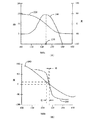
VCOは、単に同調可能な発振器でしかない。典型的な発振器回路はアンプと共振回路とから成るものであるが、一般には、共振回路と呼ばれている。結果の発振器は、利得が1よりも大きく且つ位相がゼロに等しい周波数出力を持つ。共振回路は、この発振周波数を設定する。その関係は、ボード線図で最も簡単に参照される。図2(A)は、典型的な発振器のためのボード線図を示している。曲線210は、左側の縦軸にデシベル表記で参照される発振器の利得であり、曲線220は、右側の縦軸に度表記で参照される位相である。点230で示されるように、発振は、発振器利得が約14dBであり且つ位相が約124MHzで発振を生じるゼロであるときに、発生する。
【0011】
VCOを構成するために、共振回路は、少なくとも一つの可変コンポーネントから成るもので、ここで、該可変コンポーネントのリアクタンスは、制御信号(典型的に電圧レベル)の関数であり、そのため、0位相の周波数、従って発信周波数もまた、変化する。VCOが広い周波数範囲にわたって同調させることを要求されるとき、上記可変コンポーネントは、広い周波数レンジにわたって共振回路を同調させることができなければならない。広い周波数範囲をカバーすることができる可変共振回路のため可能な回路構成は、非常に敏感な可変コンポーネントを組み込んだ共振回路、又は、広範な制御電圧レンジを必要とする共振回路を含む。MHz/Vで測定されるVCO利得が非常に高くなるので、第一の選択肢は幾つか問題点がある。これは、比較的小さな制御電圧の変化で大きく周波数を変化させてしまうこととなり、同調ライン上に誘発されたノイズに、より影響され易いVCOとなってしまう。また、要求される制御電圧レンジが非常に広いので、第二の選択肢も問題がある。大きな制御電圧は、限られた利用可能供給電圧レンジしか持たない移動式バッテリ駆動電子機器において問題となる。
【0012】
独特の周波数バンドがサポートされなければならない応用においては、広い同調レンジをカバーするようVCOを設計する第三の選択肢がとられることができる。この状況は、一般にデュアル・バンド無線電話の設計において発生する。無線電話は、セルラ・バンド(送信バンド824〜849MHz、受信バンド869〜894MHz)及びパーソナル通信システム(PCS)バンド(送信バンド1850〜1910MHz、受信バンド1930〜1990MHz)で動作するのが最も一般的である。一台の電話が、セルラ・バンドとPCSバンドの両方で動作するよう設計されることができる。電話内部の周波数計画は、典型的に、発振器の数を最小にし、それによって、電話のコストを最小にするように設計される。しかしながら、最も賢明な周波数計画でさえも、一方のバンドで動作するときと他方のバンドで動作するときでは、異なるL0周波数を必要とする。セルラ動作バンドとPCS動作バンドの両方をサポートするために、発振器の共振回路中で、複数のコンポーネントが選択的に切り換えられる。そのような複数コンポーネントは、発振器の共振回路内に含められるものであり、ダイオード・スイッチを使用して切り換えられる。回路の動作周波数は、そのようなスイッチのために使用されるダイオードの種類を制限する。スイッチが閉位置にあるときには、ダイオードは、最小の抵抗を維持すると同時に、変化するRF電流を流すことができなければならない。スイッチが開位置にあるときには、ダイオードは、RF電圧を絶縁し且つ高い抵抗を維持することができなければならない。一般には、他の種類のダイオードがスイッチとして使用されることができるとはいえ、PINダイオード・スイッチがRF周波数でのスイッチのために使用されている。さらに、上記回路はダイオード・スイッチの使用に限られるものではない。閉位置でRF電流を流すことができ且つ開位置でRF絶縁ができるいかなるスイッチも、上記回路内に組み込まれることができる。
【0013】
ダイオード・スイッチが順方向バイアスされると、切換型コンポーネントが、共振回路内でアクティブになる。ダイオード・スイッチが順方向バイアスされないときには、上記コンポーネントは、共振回路に電気的に寄与しない。共振回路内のコンポーネントの切り換えは、VCO利得を対応して増加させることなしに、発振器の同調レンジを大きく広げる。
【0014】
共振回路は、所望の動作周波数に発振器を同調させるには十分なものでない。共振回路のQは、所定の制御電圧レベルで特定の出力周波数を維持するのに重要である。図2(B)は、異なるQ値を持つ二つの共振回路の位相応答を示すものである。より低い回路Qは、よりゆるやかな位相応答を生成するのに対し、より高い回路Qは、より鋭い位相応答を生成する。より高い回路Qは、出力周波数の小さい位相変動の影響を最小にすることを要求される。比較的低い回路Qを持つ回路の位相応答は、曲線240で示される。曲線250は、より高い回路Qを持つ回路を示している。ある位相変動のために、より低い回路Qを持つ回路で周波数変化がより大きいということが参照されることができる。ある位相変動のための低いQの回路の周波数変化f2の大きさは、同じ位相変動のための高いQの回路の周波数変化f1の大きさよりも大きい。
【0015】
特定用途向け集積回路は、多くの無線電話機能を一つのICに組み込むのに有効なものである。周波数シンセサイザICは、必要とされたシンセサイザ回路のほとんど全てを一つのチップ上に組み込むのに有効である。典型的に、これらのICの一つのユーザは、合成されたLOを生成するために、当該ICに加えて、共振回路、ループ・フィルタ及び基準発振器を提供する必要があるだけである。シンセサイザの残りの構成要素である、VCOのアンプ部分、分周器、及び位相検波器が、一つのICへ組み込まれる。ユーザは、所望の出力周波数を発生するのに必要とされる共振回路を提供する。ユーザは、また、所望のループ・バンド幅を発生する低域通過フィルタ設計を提供する。
【0016】
特定用途向けICが、無線電話内部でのLOの発生を単純化するとはいえ、無線電話操作環境は、熟考されなければならない追加のノイズ源を提供する。無線電話のコスト及びスペースの制限は、有効なノイズ・フィルタリング解法をさらに束縛する。
【0017】
移動式電話の設計は、それがサポートする特定の移動式システムに依存して、非常に異なるものである。移動式電話設計を概説している仕様は、通信工業会(TIA)/電子工業会(EIA)IS−95−B、デュアルモード・スペクトル拡散方式のための移動局‐基地局互換性基準(MOBILE STATION−BASE STATION COMPATABILITY STANDARD FOR DUAL−MODE SPREAD SPECTRUM SYSTEMS)や、TIA/EIA IS−98−B、デュアルモード・スペクトル拡散セルラ移動局のための勧告された最小限の性能基準(RECOMMENDED MINIMUM PERFORMANCE STANDARDS FOR DUAL−MODE SPREAD SPECTRUM CELLULAR MOBILE STATIONS)を含む。パーソナル通信システム(PCS)バンドでのCDMAシステムの動作をカバーする仕様は、アメリカ規格協会(ANSI)J−STD−008、1.8〜2.0GHz符号分割多元接続(CDMA)パーソナル通信システムのための個人局‐基地局互換性要件(PERSONAL STATION−BASE STATION COMPATIBILITY REQUIREMENTS FOR 1.8 TO 2.0 GHZ CODE DIVISION MULTIPLE ACCESS (CDMA) PERSONAL COMMUNICATIONS SYSTEMS)である。同様に、電話即ち個人局は、ANSI J−STD−018、1.8〜2.0GHz符号分割多元接続(CDMA)個人局のための勧告された最小限の性能要件(RECOMMENDED MINIMUM PERFORMANCE REQUIREMENTS FOR 1.8 TO 2.0 GHZ CODE DIVISION MULTIPLE ACCESS (CDMA) PERSONAL STATIONS)で定められている。さらに、移動式電話の仕様は、電話ハードウェアで実現されるとき、電話内部のノイズ源を増加させる傾向があるという特徴を顕著にする。
【0018】
IS−95及びJ−STD−008で定められたようなCDMA電話システムで利用される1つの有益な特徴は、複数のデータ・レート・セットである。無線電話通信リンクの可変の性質の利点を受け取るために、CDMA仕様は、減じられたレートでのデータ送信を提供する。人が電話で会話しているとき、一方の当事者だけが話している期間が多くある。減じられたスピーチ活動の期間の間、電話は、送信のデータ・レートを減らし、平均送信パワー・レベルをより低くすることができる。
【0019】
無線電話から基地局への通信リンクは、逆方向リンクと呼ばれる。上記逆方向リンク上では、平均送信パワーの減少は、活動が低い期間の間、その時間の一部で送信機をオフにすることによって成し遂げられる。CDMA逆方向リンクでは、電話は常に最大限のデータ・レートで送信するが、しかしながら、内部構造が減じられたデータ・レートでの動作を許すときには、データは多数回繰り返される。一例として、電話が最大限のデータ・レートの半分で動作することができるとき、情報は、送信されたデータ・レートを最大限のデータ・レートまで持ってくるために、二回繰り返される。同様に、1/4のレート・データは、最大限のデータ・レートを成し遂げるために、4回繰り返される。
【0020】
逆方向リンクで節電するために、各20mSデータ・フレームは、16個の1.25mS時間グループに細分される。電話が最大限のデータ・レートで動作しているとき、フレーム内の16個全てのグループが送信される。しかしながら、電話が減じられたデータ・レートで動作するときには、16個のグループの一部分だけが送信される。送信されたグループの部分は、データ・レートにおける減少と等しい。電話が半分で動作するとき、最大限のデータ・レートの半分のグループが送信される。しかしながら、データがデータ・レート減少に反比例で繰り返されるので、データは消失しないという点に注意されたい。半分のレート・データが二回繰り返されるが、しかし、半分のデータだけが送信される。データの重複した部分は、送信されない。同様に、1/8のレート・データは8回繰り返されるが、しかし、1/8のデータだけが送信される。
【0021】
電話が減じられたデータ・レートで動作するとき、電力は送信経路上のアクティブ回路を選択するためにゲート制御される。データが送信されていないときには、上記回路への電力はオフにゲート制御される。電力は、所望のデータ・グループの送信に先立って、上記回路をオンに戻すようゲート制御される。電力ゲート制御は、無線電話内部の電力を節約するために働く。これは、非常に切望されている延長したバッテリ寿命になる。
【0022】
電力ゲート制御の逆の影響は、電話の電源に突然の負荷変化を与えるということである。オン/オフ切り換えされるRF送信経路の部分は、電源に対して最も大きな負荷を与える。従って、電力ゲート制御の間、電話の電源は、それが経験するだろう最も大きな負荷変動を受ける。電源が負荷変動に無感応ではないので、電力ゲート制御が発生するレートで、電源の出力は電圧リップルを見せるだろう。給電ライン上の実際の電圧リップルは、電源負荷除去と、電力ゲート制御のレートと、電力ゲート制御のための電源負荷の変化との関数である。電源負荷の変化は、当該電話が基地局と維持しているRF通信リンクに関して変化する。負荷電流の変化は、電話が減少されたRF電力レベルで送信しているときよりも、電話がより高いRF電力レベルで送信しているときのほうが大きいだろう。電力ゲート制御は、逆方向リンク上で各データ・フレームのために使用される各1.25のmS時間グループで発生することができる。これは、重要な800のHz周波数コンポーネントで、電源負荷変動を引き起こす。
【0023】
一定の制御電圧の印加で、安定した出力周波数を維持する電圧制御発振器設計が望まれている。VCOは、二つの別個の周波数バンドで同調されるように切り換えられることができなければならない。さらに、VCO出力は、電源ノイズに無感応でなければならない。特に、VCOがCDMA電話内部に組み込まれるとき、VCO出力は、RF送信経路の電源ゲート制御によって発生する電源ノイズに無感応でなればならない。本発明の別の目的は、VCO内の共振回路として使用するための、高いQ、低コスト、少コンポーネント数の、コンポーネント切り換え型の、ノイズに無感応な回路の設計である。
【0024】
発明の要約
本発明は、よりノイズに強い、新規且つ改善された複数バンド電圧制御発振器(VCO)である。さらに、本発明は、切換型コンポーネントを含み、高いQを持ち、且つ、ノイズに無感応である、新規な共振回路構成と見られることができる。新規な共振回路は、複数バンドのカバーレージ、ノイズ無感応、及び周波数安定性の特徴を持つVCOを構成するために、アンプ又は特定用途向けICで実現されることができる。
【0025】
第一の実施形態においては、共振回路の構成要素の全ては、インダクタを除いて、バランス型構成で接続される。第一及び第二の結合コンデンサは、共振回路への正及び負平衡接続を含む。上記第一及び第二の結合コンデンサの出力は、スイッチト・キャパシタと直列のインダクタとを使用して、互いに接続されている。第一の同調コンデンサは、第一の結合コンデンサの出力を第一の可変コンデンサに接続する。第二の同調コンデンサは、第二の結合コンデンサの出力を第二の可変コンデンサに接続する。第一及び第二の可変コンデンサの反対側は共に接続され、それによって、共振回路の平衡接続に関してバランス型構成を維持する。ダイオード・スイッチは、該ダイオード・スイッチが順方向バイアスされないときに、上記スイッチト・キャパシタが共振回路に電気的に接続されるように、上記スイッチ・キャパシタに並列接続されている。上記ダイオード・スイッチが順方向バイアスされたときには、上記スイッチト・キャパシタは上記共振回路に電気的に接続されない。
【0026】
第一の実施形態においては、第一及び第二の同調コンデンサは、電圧制御型可変回路として利用される。第一の実施形態においては、上記可変回路の静電容量値は、制御電圧の印加で変化させられる。制御電圧を使用して共振周波数を同調できるように、そのインピーダンスが印加された電圧に従って変化する種類の可変回路が共振回路中に使用されることができる。本発明で述べられた好ましい実施形態は、そのような可変回路として、可変コンデンサを利用する。
【0027】
上記スイッチの動作によって、上記VCOの中心周波数が二つの値、f1とf2、の間でシフトするようになる。より詳細には、上記スイッチの駆動によって、共振回路の共振周波数が変化するようになり、それによって、f1とf2の間でVCOの中心周波数をシフトする。
【0028】
第一の実施形態は、回路Qを最大にするという効果を持つ。これは、一つのインダクタだけが回路中で利用されるからである。インダクタQは、高い回路Qを成し遂げることへの制約である。回路中の多数のインダクタの除去は、回路Qを最大にする。しかしながら、この回路は、第二の実施形態ほどノイズに無感応なものではない。
【0029】
第二の実施形態においては、共振回路の構成要素の全てが、バランス型構成で接続される第一及び第二の結合コンデンサは、まさに第一の実施形態におけるように、共振回路へ正及び負平衡接続を含む。上記第一及び第二の結合コンデンサの出力は、第一及び第二のインダクタに接続される。上記第一及び第二のインダクタは、上記結合コンデンサの一方とグラウンドとにそれぞれ接続している。第一の同調コンデンサは、上記第一の結合コンデンサの出力を第一の可変コンデンサに接続する。第二の同調コンデンサは、上記第二の結合コンデンサの出力を第二の可変コンデンサに接続する。上記第一及び第二の可変コンデンサの反対側は共に接続され、それによって、共振回路の平衡接続に関してバランス型構成を維持する。第二の実施形態は、後述するように、共振回路の入力に関して完全にバランスされている。スイッチト・キャパシタの一端は、上記第二の結合コンデンサの出力に接続されている。このスイッチト・キャパシタは、上記第一の結合コンデンサの出力に接続されたダイオード・スイッチに直列に接続されている。上記第一の結合コンデンサの出力は、上記ダイオード・スイッチと直列の上記スイッチト・キャパシタを使用して、上記第二の結合コンデンサの出力に接続されている。共振回路は、上記スイッチト・キャパシタが、上記第二の結合コンデンサの出力に接続された上記ダイオード・スイッチと共に上記第一の結合コンデンサの出力に接続されているかどうか、即ち、上記スイッチト・キャパシタの位置と上記ダイオード・スイッチの位置が置き換えられるかどうかは、重要なものでない。
【0030】
上記スイッチの動作によって、VCOの中心周波数が二つの値、f1とf2、の間でシフトするようになる。より詳細には、上記スイッチの駆動によって、共振回路と関連した静電容量が変化するようになり、それによって、共振回路の共振周波数をシフトし、従って、VCOの中心周波数をf1からf2へ変化させる。
【0031】
また、第二の実施形態は、高域通過フィルタの追加のポールのため、よりノイズに強い。入力側から見ると、平衡入力の各々は、高域通過フィルタを効果的に持つ。これは、インダクタに関する結合コンデンサの構成による。この高域通過フィルタは、共振回路上に誘発されたノイズの大多数を除去するのに効果的に機能する。ノイズが、可変コンデンサに影響を及ぼすことから除去され、それによって、共振回路の動作に対する誘発されたノイズの影響を除去する。
【0032】
好ましい実施形態の詳細な説明
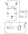
図3は、無線電話中で使用される一般的な局部発振器の構成を示すブロック図である。合成発振器IC300は、位相同期ループ(PLL)302と、発振器304として構成されたアンプとを組み込んだものである。合成発振器IC300は、動作するために、外部の共振回路とループ・フィルタ310とを必要とする。上記共振回路が制御電圧の印加によって同調されることができるならば、発振器304は電圧制御発振器(VCO)として構成される。
【0033】
上記共振回路は、容量性ネットワークと、それに並列なインダクタ320とから成る。上記容量性ネットワークは、直列に接続された第一及び第二の可変コンデンサ342及び344を利用する。上記第一の可変コンデンサ342は、第一の同調コンデンサ332を介して、上記インダクタ320の第一の端部に接続されている。上記第二の可変コンデンサ344は、第二の同調コンデンサ334を介して、上記インダクタ320の第二の端部に接続されている。上記第一の可変コンデンサ342と上記第二の可変コンデンサ344との接続点は、信号用グラウンドに連結されている。
【0034】
上記合成発振器IC300内の上記発振器304は、上記共振回路の周波数で動作する。上記発振器304の出力のサンプルが、上記PLL302に送られる。上記PLL302は、上記発振器304の出力信号の位相を基準信号(図示せず)と比較する。結果として生じる誤差信号が、ループ・フィルタ310に渡され、そこから上記共振回路に印加される。上記ループ・フィルタ310の出力は、第一及び第二のバイアス抵抗器352及び354を介して、上記可変コンデンサ342及び344に印加される。上記第一のバイアス抵抗器352は、上記ループ・フィルタ310の出力端を、上記第一の可変コンデンサ342の上記第一の同調コンデンサ332に接続された端子に接続する。同様に、上記第二のバイアス抵抗器354は、上記ループ・フィルタ310の出力端を、上記第二の可変コンデンサ344の上記第二の同調コンデンサ334に接続された端子に接続するのに使用される。上記第一の可変コンデンサ342及び上記第二の可変コンデンサ344は、バラクタ・ダイオードとして実現されることができる。上記ループ・フィルタ310の出力は、これらバラクタ・ダイオードの逆バイアスに使用される。バラクタ・ダイオードは、印加された逆バイアスのレベルに基づいてその静電容量値を変化させるものである。従って、上記バラクタ・ダイオードの逆バイアス電圧を制御することによって、上記発振器の周波数が制御されることができる。上記制御電圧は、上記PLL302の位相同期を維持するために変えられる。
【0035】
図3に示されるように無線電話LOが構成されるとき、上記発振器304は、上記共振回路のレンジで同調することができるだけである。電話が複数の周波数バンドをカバーすることができるような広い周波数スパンで同調することを上記発振器304が必要とされるならば、上記共振回路は上記全レンジで同調可能でなければならない。広いレンジでの図3の共振回路の同調は、二つの方法で成し遂げられることができる。
【0036】
第一の方法は、非常に高感度の可変コンデンサ342及び344を利用するものである。非常に高感度な可変コンデンサが使用されると、制御電圧レンジは最小限の値に維持される。しかしながら、上記可変コンデンサの感度は、上記共振回路を、当該回路上で誘発されたノイズに敏感にする。上記可変コンデンサ・バイアスで誘発されたノイズのいかなる源も、上記回路の共振周波数にシフトを引き起こす。誘発されたノイズのレートがループ帯域幅より高いならば、上記PLL302は、誤差を訂正することができない。
【0037】
第二の方法は、広げた制御電圧レンジで、低感度の可変コンデンサを利用するものである。しかしながら、上記広げた制御電圧レンジは、バッテリ電力で動作する無線電話のためには問題となる。バッテリによって提供される電圧は比較的低いので、上記制御電圧レンジの拡大は、使用可能な電圧のステップ・アップを必要とする。電圧のステップ・アップは、DC−DCコンバータで成し遂げられる。DC−DCコンバータは、100%効率で動作するものではない。上記ステップ・アップ電圧変換での損失は、浪費されたバッテリ電力である。バッテリ電力消費を最小にすることは、無線電話では重大なプライオリティである。無線電話における別の重大なプライオリティは、物理的なサイズを最小にすることである。これらプライオリティの高い設計制約は両方とも、無線電話での広げた制御電圧レンジの使用を妨げる。
【0038】
代わりの共振回路構成は、切換型コンポーネントを上記共振回路に組み込むものである。上記コンポーネントは、第一の周波数帯での動作のためには上記共振回路から切換切断され、また、第二の周波数帯での動作のためには、上記コンポーネントは上記共振回路に切換接続される。
【0039】
本発明の第一の実施形態は、図4に示されている。上記LO構成は、図3で述べられたのと同様の合成発振器IC300とループ・フィルタ310とを利用する。しかしながら、図4における共振回路の構成は、図3で示されたものとは異なっている。図4に示された共振回路は、上記回路に対し、ダイオード・スイッチ420のバイアスに従って、切換接続及び切換切断されることができるスイッチト・キャパシタ414を含む。しかしながら、図4に示される共振回路は、図3の共振回路には組み込まれていない追加の構成要素を含んでいる。
【0040】
図4に示された共振回路は、第一及び第二の結合コンデンサ402及び404を組み込んでいる。これらの結合コンデンサは、上記発振器のピンから上記共振回路までのいかなるノイズのレベルをも減少させるだろう。各結合コンデンサの第一の端子は、上記共振回路を上記発振器304のそれぞれの端子に接続するために使用される。各結合コンデンサ402及び404の第二の端子は、上記共振回路の残りの反対側の端部に接続されている。上記第一の結合コンデンサ402の上記第二の端子は、スイッチト・キャパシタ414と直列に配置されているインダクタ410に接続されている。上記スイッチト・キャパシタ414の上記インダクタに接続されていない側の端部は、上記第二の結合コンデンサ404の上記第二の端子に接続されている。
【0041】
ダイオード・スイッチ420が、上記スイッチト・キャパシタ414と並列に接続されている。上記ダイオード・スイッチ420のアノードは、上記第二の結合コンデンサ404の上記第二の端子に接続され、上記ダイオード・スイッチ420のカソードは、上記インダクタ410と上記スイッチト・キャパシタ414との接合部に接続されている。上記ダイオード・スイッチ420のアノードは、プル・アップ抵抗器462を使用して給電レールにプル・アップされている。上記第一の結合コンデンサ402と上記インダクタ410の接合部に接続されているのは、上記ダイオード・スイッチ420の順方向バイアスを制御するために使用される回路である。この回路は、DCスイッチ466に接続されたプル・ダウン抵抗器464を含む。上記DCスイッチ466が閉じられると、上記プル・ダウン抵抗器464は、上記インダクタ410からのDC経路を開放し、電流は該DC経路を流れない。上記DCスイッチ466に接続された制御抵抗468を駆動する帯域選択信号が、上記DCスイッチ466を制御する。上記スイッチト・キャパシタ414に並列に配置された上記スイッチの構成は、重要ではない。図4に示された上記順方向バイアスされたダイオード・スイッチ420は、一例でしかなく、上記共振回路で使用されることができるスイッチ構成を何ら限定するものではない。上記スイッチト・キャパシタ414と並列に配置されるいかなる類似のスイッチも許される。
【0042】
図4の共振回路の残りのものは、図3に示されたものと非常に類似の構成である。第一の同調コンデンサ432は、上記第一の結合コンデンサ402の上記第二の端子を第一の可変コンデンサ442に接続する。第二の同調コンデンサ434は、上記第二の結合コンデンサ404の上記第二の端子を第二の可変コンデンサ444に接続する。上記二つの可変コンデンサ442及び443の上記同調コンデンサ432及び434と反対側の端部は、共に接続され、グラウンドに連結されている。上記ループ・フィルタ310からの上記制御電圧信号は、バイアス抵抗器452及び454を介して、上記可変コンデンサ442及び444の各々に印加される。第一のバイアス抵抗器452は、上記ループ・フィルタ310からの上記制御電圧信号を、上記第一の可変コンデンサ442と第一の同調コンデンサ432との接合部に接続する。第二のバイアス抵抗器454は、上記ループ・フィルタ310からの上記制御電圧信号を、上記第二の可変コンデンサ444と第二の同調コンデンサ434との接合部に接続する。上記バイアス抵抗器452及び454は、上記可変コンデンサ442及び444がバラクタ・ダイオードとして実現されるとき、上記制御電圧信号を上記可変コンデンサに逆バイアスで印加する。本実施形態においては、上記制御電圧は、0〜3ボルトに変えられることができる。上記制御電圧信号は、コンポーネント中の変動や温度変動のために本発明を調節するのに使用される。
【0043】
本第一の実施形態の周波数バンド・スイッチの能力は、以下のように述べられる。上記DCスイッチ466が閉じられると、上記ダイオード・スイッチ420は、順方向にバイアスされ、導通する。上記ダイオード・スイッチ420が導通すると、上記スイッチト・キャパシタ414は短絡され、電気的に上記共振回路に寄与しない。そして、上記共振周波数f1は、上記可変コンデンサ442及び444に関して、上記同調コンデンサ432及び434から成る容量性の同調回路と並列な上記インダクタの値によって決定される。上記帯域選択信号が上記DCスイッチ466を開放状態に制御するとき、上記ダイオード・スイッチ420はもはや導通しない。
【0044】
上記ダイオード・スイッチ420が導通していないとき、上記スイッチト・キャパシタ414は、電気的に上記共振回路に接続される。上記スイッチト・キャパシタ414が電気的に上記共振回路に寄与するとき、上記回路の上振周波数f2は増大される。上記スイッチト・キャパシタ414が上記インダクタ410と直列に現れるので、上記共振周波数f2は増大される。上記直列の組合せは、各リアクタンスの合計であるリアクタンスになる。インダクタのリアクタンスがコンデンサのリアクタンスとは反対であるので、直列の組合せの効果は、上記二つのリアクタンスのうちの大きい方よりも小さいリアクタンスである。上記スイッチト・キャパシタ414のリアクタンスは、上記二つの構成要素の直列の組合せが、同等により小さいインダクタのリアクタンスを持つように、上記インダクタ410のリアクタンスよりも小さくなるよう選択される。上記共振回路中のインダクタが小さくなれば、上記共振周波数がより高くなる。
【0045】
図4に示された本発明の第一の実施形態は、いくつかの効果を奏する。一つ効果は、本実施形態が回路Qを最大にするということである。上記回路が最小限の数のインダクタで実現されるので、上記回路Qは最大にされる。その物理的な構造のため、インダクタは、コンデンサよりも非常に低いコンポーネントQと、コンデンサよりも大きなサイズを持つ。インダクタの追加及び除去によってバンド切り換えを成し遂げる共振回路は、コンデンサの追加及び除去によってバンド切り換えを成し遂げる共振回路よりも低い回路Qを持つだろう。また、回路Qは、上記インダクタ410とスイッチト・キャパシタ414の直列組合せによって、最大にされる。より大きいインダクタ410の値が使用されるので、上記回路Qは、上記インダクタ410とスイッチト・キャパシタ414の上記直列組合せで、より高い。インダクタ410のコンポーネントQがXL/RLとして決定されるので、インダクタンスがより大きな値となれば、コンポーネントQはより大きくなる。また、コンデンサ値がインダクタ値よりも細かい階調で使用可能であるので、インダクタとそれより高いコンデンサとを使用する二つの動作周波数の中心を見出すことは、より簡単である。
【0046】
本第一の実施形態の別の効果は、ノイズに対する強さをより強くするということである。CDMA無線電話システムにおける減じられたレートでの送信の間、電力を節約するために、送信経路の回路がゲート制御でパワー・オン/オフされるとき、上記電源負荷の突然の変化は、上記電源出力の変動を引き起こす。上記電源出力の変動は、全ての能動部分に影響を及ぼす。上記合成発振器IC300は、上記電源変動によって影響を受け、全ての出力ライン上に、対応する電圧リップルを現すことがある。上記電圧リップルは、上記ループ・フィルタ310への上記制御電圧ライン上に加えて、上記共振回路につながる端子上に現れるだろう。
【0047】
上記二つの結合コンデンサ402及び404は、発振器ピンを介して上記共振回路上に誘発されたいかなるノイズの影響も減少させるのを助ける。上記結合コンデンサ402及び404は、上記可変コンデンサ442及び444に最終的に到達する電圧リップルのレベルを減らすのに役立つ追加のリアクタンスを提供する。
【0048】
上記共振回路のバンド切換構成は、上記VCO利得を最小にすることによって、よりノイズに強いものとなる。上記VCO利得は、上記VCOの同調感度の尺度であり、Kvで表され、一般にMHz/Vの測定単位である。上記バンド切換構成は、上記共振回路中の上記可変コンデンサの必要とされる静電容量変化を制限することによって、上記VCO利得を最小にする。周波数バンドを切り換えるのに必要とされる大規模な変更が上記スイッチト・キャパシタ414の包含によって行われるので、静電容量レンジは最小にされる。従って、制限された電圧制御レンジは、Kvの値を増大することなしに両方のバンドで発振器周波数を正確に制御することができる。本第一の実施形態においては、L及びCの値は、上記Kv値が、動作周波数f1及びf2でほぼ同じであるように、選択される。
【0049】
図5に示される本発明の第二の実施形態は、回路Qのわずかな低下で、より一層、ノイズに強くするものである。また、この第二の実施形態は、バンド切換共振回路構成を利用する。本第二の実施形態は、上記第一の実施形態と非常に同様のものである。
【0050】
本第二の実施形態は、共振回路への入力として、第一及び第二の結合コンデンサ502及び504を組み込んでいる。上記合成発振器IC300は、外部の共振回路のために、一対の平衡接続を持っている。上記第一の結合コンデンサ502の第一の端子は、上記合成発振器IC300の正共振回路インタフェース結合部に接続している。上記第一の結合コンデンサの第二の端子は、第一のインダクタ512に接続している。上記第一のインダクタ512は、グラウンドへの回路経路を提供する。同様に、上記第二の結合コンデンサ504の第一の端子は、上記合成発振器IC300の負共振回路インタフェース結合部に接続している。上記第二の結合コンデンサ504の第二の端子は、第二のインダクタ514に接続している。上記第二のインダクタ514は、グラウンドへの回路経路を提供する。
【0051】
ダイオード・スイッチ520とそれに直列なスイッチト・キャパシタ522は、上記第一の結合コンデンサ502の上記第二の端子を、上記第二の結合コンデンサ504の上記第二の端子に接続する。上記ダイオード・スイッチ520のアノードは、直列接続で上記スイッチト・キャパシタ522に接続されている。図5は、上記スイッチト・キャパシタ522が、上記第二の結合コンデンサ504の上記第二の端子に接続され、上記ダイオード・スイッチ520のカソードが、上記第一の結合コンデンサ502の上記第二の端子に接続されていることを示している。しかしながら、上記スイッチト・キャパシタ522とダイオード・スイッチ520の直列接続は、当該回路の動作に影響を及ぼすことなく、逆にすることができる。即ち、回路動作の変化なしで、上記ダイオード・スイッチ520のカソードが、上記第二の結合コンデンサ504の上記第二の端子に接続され、上記スイッチト・キャパシタが、上記第一の結合コンデンサ502の上記第二の端子に接続される。
【0052】
上記ダイオード・スイッチ520をバイアスするのに必要とされる回路は、一端が上記ダイオード・スイッチ520のアノードに接続され、他端がDCスイッチ566に接続された、プル・アップ抵抗器564を含む。上記DCスイッチ566は、閉じられた状態で上記プル・アップ抵抗器564を電源レールに接続する。上記DCスイッチ566が閉じられたとき、DC電流の流れは、上記プル・アップ抵抗器564、順方向バイアスされた上記ダイオード・スイッチ520、及び上記第一のインダクタ512を介してグラウンドへの経路をたどる。上記DCスイッチ566が開状態にあるときには、上記プル・アップ抵抗器564は開放とされ、電流は上記プル・アップ抵抗器564を流れない。上記DCスイッチ566の制御端子に接続された制御抵抗568を駆動する帯域選択信号が、上記DCスイッチ566の動作を制御する。
【0053】
共振回路の残りの部分は、上記第一の実施形態におけるものと同様の手段で構成されている。第一の同調コンデンサ532は、上記第一の結合コンデンサ502の上記第二の端子を、第一の可変のコンデンサ542に接続する。第二の同調コンデンサ534は、上記第二の結合コンデンサ504の上記第二の端子を、第二の可変コンデンサ544に接続する。上記二つの可変コンデンサ542及び544の、上記同調コンデンサ532及び534とは反対側の端部は、共に接続され、グラウンドに連結される。上記ループ・フィルタ310からの制御電圧信号は、バイアス抵抗器552及び554を介して、上記可変コンデンサ542及び544の各々に印加される。第一のバイアス抵抗器552は、上記ループ・フィルタ310からの上記制御電圧信号を、上記第一の可変コンデンサ542と第一の同調コンデンサ532との接合部に接続する。第二のバイアス抵抗器554は、上記ループ・フィルタ310からの上記制御電圧信号を、上記第二の可変コンデンサ544と第二の同調コンデンサ534との接合部に接続する。上記バイアス抵抗器552及び554は、上記可変コンデンサ542及び544がバラクタ・ダイオードとして実現されるとき、上記制御電圧信号を上記可変コンデンサに逆バイアスで印加する本実施形態においては、上記制御電圧は、0〜3ボルトに変えられることができる。上記制御電圧信号は、コンポーネント中の変動や温度変動のために本発明を調節するのに使用される。
【0054】
本発明の第二の実施形態も、バンド切換発振器を実現する。上記ダイオード・スイッチ520が順方向バイアスされると、上記スイッチト・キャパシタ522は、電気的に上記共振回路に接続される。上記スイッチト・キャパシタ522は、上記共振回路中で、上記同調コンデンサ532及び534と上記可変コンデンサ542及び544とから成る容量性ネットワークと並列に現れる。従って、上記スイッチト・キャパシタ522は、上記共振回路における静電容量値を増大する。その効果は、上記共振回路の共振周波数をf1に下げることである。ダイオードがオフのときには、上記回路はより高い共振周波数f2で動作する。本第二の実施形態における共振回路は、バンド切換共振回路の使用を通しての両方の発振器周波数バンドでのカバーレージを提供することによって、低い値のVCO利得Kvを維持する。
【0055】
本第二の実施形態の共振回路の主要な効果は、ノイズに対する強さに関してである。上記第一の実施形態の場合と同様に、本第二の実施形態は、バンド切換構成を利用していない広帯域発振器と比較されるとき、より強いノイズに対する強さを提供する。上記バンド切換発振器におけるより低いVCO利得Kvの値は、そのバンド切換発振器を、制御電圧ライン上に誘発されたノイズに、より敏感にする。上記ループ・フィルタ310が上記制御電圧ライン上に誘発されたノイズの大多数を除去するだろうとはいえ、上記ノイズの全てが除去されるというわけではないだろう。上記広帯域発振器の制御電圧ライン上の同等の電圧リップルは、より大きい周波数逸脱になるだろうし、そして、上記バンド切換発振器の制御電圧ライン上に同様の電圧リップルを誘発することになるだろう。バンド切換設計のためのノイズに対する強さの改良は、二つの発振器設計のためのVCO利得の比率である。
【0056】
上記共振回路の完全な平衡設計はまた、共振回路への入力に誘発されたノイズに対する増大された強さを生ずる。どちらの入力端子から見ても、上記共振回路は高域通過フィルタとして構成される。分路中の上記第一又は第二のインダクタ512又は514の何れかに関連する直列結合コンデンサ502又は504の組合せは、二つのポール高域通過フィルタを生ずる。上記高域通過フィルタ構成は、上記合成発振器IC300からノイズを除去する際に特に役に立つ。上記合成発振器IC300からのノイズの一つの特定の源は、送信信号経路中のアクティブ装置の電力サイクリングに対応する電源電圧変動に起因している。上記送信信号経路中のアクティブ装置の電力サイクリングは、CDMA無線電話が減じられたデータ・レートで動作するときに発生する。上記CDMA電話が減じられたデータ・レートで動作しているときには、多数繰り返されるデータ期間のうちの一つのコピーだけが送信される。これは、上記電話の節電になるだけでなく、上記電話から送信される平均RF電力の減少にもなる。上記減じられた平均電話RF送信電力は、同じバンドで動作している他の電話に対し、より小さい妨害にしかならない。送信電力サイクリングは、重要な800Hz周波数コンポーネントで、電源ノイズになる。上記電源ノイズは、上記合成発振器IC300のインタフェース結合部を通して上記共振回路上に誘発される。上記共振回路の設計に組み込まれた高域通過フィルタは、上記可変コンデンサ542及び544からノイズを除去する。その結果は、上記共振回路中の他のいかなるコンポーネントも電圧変動によって影響を受けないので、上記共振回路は上記合成発振器IC300から誘発されたノイズに影響されないということである。そして、上記共振回路がノイズによって影響を受けないので、上記発振器304の出力は、より良好な位相ノイズを現す。
【0057】
本発明は、要求された特徴の大多数を持つ発振器を提供する。上記共振回路の高いQは、上記発振器が所定の制御電圧のために安定した動作周波数を維持することを確実にする。上記バンド切換設計は、VCO利得の低い値を維持すると同時に、上記発振器が複数の周波数バンドをカバーするのを許す。これは、制御電圧ライン上のノイズに対し上記VCO出力の感度を下げることによって、上記発振器出力の位相ノイズを改善する。最も重大なのは、上記共振回路設計は、誘発されたノイズに比較的強いということである。合成発振器ICのようなアクティブ発振器回路から誘発されたノイズは、それが共振回路内の同調構成要素上で影響を持つことができる前に、上記共振回路中でフィルタリングされる。上記フィルタは、高域通過構成に上記共振回路の構成要素を組み立てることによって構成される。従って、上記共振回路を構成するまさしくその構成要素は、同時に、いかなるノイズもフィルタリングするのに役立つ。その結果は、上記発振器回路の雑音が多い操作環境に関係なく、純粋な発振器出力である。
【0058】
以上の好ましい実施形態の説明は、いかなる当業者も本発明を実施即ち使用できるようにするために提供されたものである。これらの実施形態への種々の修正は、当業者には容易であることは明らかであり、ここで定義された包括的な原理は、発明能力の使用なしで、他の態様に適用することができる。従って、本発明は、ここで示された上記実施形態に限定されるものではなく、ここに開示された原理及び新規な特徴と一致した最も広い範囲に一致させられるべきである。
【図面の簡単な説明】
【図1】
合成局部発振器のブロック図である。
【図2】
(A)及び(B)はそれぞれ発振器回路を特徴づける振幅プロット及び位相プロットを示す図である。
【図3】
集積回路合成発振器のブロック図である。
【図4】
集積回路発振器に組み込まれた本発明の第一の実施形態を示すブロック図である。
【図5】
集積回路発振器に組み込まれた本発明の第二の実施形態を示すブロック図である。
【符号の説明】
300 合成発振器IC
302 位相同期ループ(PLL)
304 発振器
310 ループ・フィルタ
402,404,502,504 結合コンデンサ
410,512,514 インダクタ
414,522 スイッチト・キャパシタ
420,520 ダイオード・スイッチ
432,434,532,534 同調コンデンサ
442,444,542,544 可変コンデンサ
452,454,552,554 バイアス抵抗器
462,564 プル・アップ抵抗器
464 プル・ダウン抵抗器
466,566 DCスイッチ
468,568 制御抵抗[0001]
Background of the Invention
1. Field of the invention
The present invention relates to an electronic circuit. More particularly, the present invention relates to a new and improved band switched voltage controlled oscillator (VCO) that is robust against noise.
[0002]
2. Conventional technology
Wireless communication systems rely on the predictable performance of wireless radio frequency (RF) links. Wireless telephone systems are required to monitor and control multiple RF links simultaneously.
[0003]
A mobile unit or radiotelephone is the union of many complex circuits. RF transceivers have been used to provide wireless communication links with base stations. This RF transceiver consists of a receiver and a transmitter. A receiver receives an RF transmission from the base station via an antenna interfaced to the mobile unit. The receiver amplifies, filters, and downconverts the received signal to a baseband signal. Then, the baseband signal is sent to the baseband processing circuit. The baseband processing circuit demodulates the signal and adapts it for broadcast to the user through speakers.
[0004]
A user input by a key operation or a voice input to a microphone is adapted in the baseband processing circuit. This signal is modulated and sent to the transmitter. A transmitter receives the baseband signal generated by the mobile unit, upconverts, filters, and amplifies the signal. The up-converted RF signal is transmitted to the base station by the same antenna used in the receiver.
[0005]
Frequency synthesizers have been used to generate the local oscillator signals needed to achieve down-conversion at the receiver and up-conversion at the transmitter. Frequency synthesis is used to generate the local oscillator signal because of the frequency stability of the synthesizer, the spectral purity of the resulting signal, and the ability to control digitally.
[0006]
Frequency synthesizers are classified into a direct type and an indirect type. In Direct Digital Synthesis, a plurality of logic circuits generate a digital representation of a desired signal, and a D / A converter is used to convert the digital representation into an analog waveform. One of the general methods for implementing DDS is to store a table of waveform phases in a memory. Then, the rate at which the phase is read from the memory is directly proportional to the frequency of the output signal. Whereas DDS can produce a very accurate representation of a sine wave, the output frequency is limited by the readout rate.
[0007]
Indirect synthesis utilizes a phase locked loop locked to the output of an oscillator. Indirect frequency synthesis is more prevalent for high frequency designs because the output of the high frequency oscillator can be divided down to a frequency within the operating range of the phase locked loop.
[0008]
FIG. 1 is a block diagram of an indirect frequency synthesizer using a phase locked loop. To provide the
[0009]
If the rate of frequency change is less than the loop bandwidth, only frequency changes at the output of
[0010]
A VCO is simply a tunable oscillator. A typical oscillator circuit includes an amplifier and a resonance circuit, but is generally called a resonance circuit. The resulting oscillator has a frequency output with a gain greater than one and a phase equal to zero. The resonance circuit sets this oscillation frequency. The relationship is most easily referenced in Bode diagrams. FIG. 2A shows a Bode diagram for a typical oscillator.
[0011]
To construct a VCO, the resonant circuit is comprised of at least one variable component, where the reactance of the variable component is a function of the control signal (typically a voltage level), and therefore has zero phase. The frequency, and thus the transmission frequency, also changes. When a VCO is required to tune over a wide frequency range, the variable component must be able to tune the resonant circuit over a wide frequency range. Possible circuit configurations for a variable resonant circuit that can cover a wide frequency range include a resonant circuit that incorporates very sensitive variable components, or a resonant circuit that requires a wide control voltage range. The first option has some disadvantages because the VCO gain, measured in MHz / V, is very high. This results in a large change in frequency with a relatively small change in control voltage, resulting in a VCO that is more susceptible to noise induced on the tuning line. Also, since the required control voltage range is very wide, the second option is problematic. Large control voltages are problematic in mobile battery-powered electronics that have only a limited available supply voltage range.
[0012]
In applications where unique frequency bands must be supported, a third option can be taken to design the VCO to cover a wide tuning range. This situation generally occurs in dual band wireless telephone designs. Wireless telephones most commonly operate in the cellular band (transmit band 824-849 MHz, receive band 869-894 MHz) and personal communication system (PCS) band (transmit band 1850-1910 MHz, receive band 1930-1990 MHz). is there. One phone can be designed to operate in both the cellular and PCS bands. The frequency plan inside the phone is typically designed to minimize the number of oscillators, and thereby the cost of the phone. However, even the smartest frequency plans require different L0 frequencies when operating in one band and when operating in the other band. Multiple components are selectively switched in the resonant circuit of the oscillator to support both the cellular and PCS operating bands. Such components are included in the resonant circuit of the oscillator and are switched using diode switches. The operating frequency of the circuit limits the type of diode used for such a switch. When the switch is in the closed position, the diode must be able to carry varying RF current while maintaining minimal resistance. When the switch is in the open position, the diode must be able to isolate the RF voltage and maintain a high resistance. In general, PIN diode switches are used for switches at RF frequencies, although other types of diodes can be used as switches. Furthermore, the above circuit is not limited to the use of diode switches. Any switch capable of conducting RF current in the closed position and providing RF isolation in the open position can be incorporated into the circuit.
[0013]
When the diode switch is forward biased, the switching component becomes active in the resonant circuit. When the diode switch is not forward biased, the components do not contribute electrically to the resonant circuit. Switching components in the resonant circuit greatly extends the tuning range of the oscillator without a corresponding increase in VCO gain.
[0014]
Resonant circuits are not enough to tune an oscillator to a desired operating frequency. The Q of the resonant circuit is important to maintain a particular output frequency at a given control voltage level. FIG. 2B shows the phase response of two resonance circuits having different Q values. A lower circuit Q produces a slower phase response, while a higher circuit Q produces a sharper phase response. Higher circuits Q are required to minimize the effects of small phase variations in output frequency. The phase response of a circuit with a relatively low circuit Q is shown by
[0015]
Application specific integrated circuits are useful for incorporating many wireless telephone functions into a single IC. Frequency synthesizer ICs are useful for incorporating almost all of the required synthesizer circuitry on a single chip. Typically, a user of one of these ICs only needs to provide a resonant circuit, a loop filter, and a reference oscillator in addition to the IC to generate a synthesized LO. The remaining components of the synthesizer, the amplifier section of the VCO, the divider, and the phase detector are integrated into one IC. The user provides the required resonant circuit to generate the desired output frequency. Users also provide low pass filter designs that produce the desired loop bandwidth.
[0016]
Although an application specific IC simplifies LO generation inside a wireless telephone, the wireless telephone operating environment provides additional noise sources that must be considered. The cost and space limitations of wireless telephones further restrict effective noise filtering solutions.
[0017]
Mobile phone designs are very different, depending on the particular mobile system that they support. Specifications outlining mobile phone design are provided by the Telecommunications Industry Association (TIA) / Electronic Industries Association (EIA) IS-95-B, Mobile Station-Base Station Compatibility Standard (MOBILE) for Dual Mode Spread Spectrum Systems STATION-BASE STATION COMPATIBILITY STANDARD FOR DUAL-MODE SPREAD SPECTRUM SYSTEMS, TIA / EIA IS-98-B, and Recommended Minimum Performance Standards for Dual Mode Spread Spectrum Cellular Mobile Stations DUAL-MODE SPREAD SPECTRUM CELLULAR MOBILE STATIONS). The specification covering operation of the CDMA system in the personal communication system (PCS) band is for the American National Standards Institute (ANSI) J-STD-008, 1.8-2.0 GHz code division multiple access (CDMA) personal communication system. PERSONAL STATION-BASE STATION COMPATIBILITY REQUIREMENTS FOR 1.8 TO 2.0 GHZ CODE DIVISION MULTIPLE ACCESS ACCESS (CDMA) PERSONAL COMMUNICATION. Similarly, the telephone or personal station may be in accordance with the recommended minimum performance requirements for ANSI J-STD-018, 1.8-2.0 GHz code division multiple access (CDMA) personal stations. .8 TO 2.0 GHZ CODE DIVISION MULTIPLE ACCESS (CDMA) PERSONAL STATIONS. In addition, the specifications of mobile phones, when implemented in phone hardware, highlight the feature that they tend to increase noise sources inside the phone.
[0018]
One useful feature utilized in CDMA telephony systems as defined in IS-95 and J-STD-008 is the multiple data rate sets. To take advantage of the variable nature of wireless telephony links, the CDMA specification provides for data transmission at a reduced rate. When a person is talking on the phone, there are many periods when only one party is talking. During periods of reduced speech activity, the telephone may reduce the data rate of the transmission and lower the average transmit power level.
[0019]
The communication link from a wireless telephone to a base station is called a reverse link. On the reverse link, a reduction in average transmit power is achieved during periods of low activity by turning off the transmitter for a portion of that time. On the CDMA reverse link, the phone always transmits at the maximum data rate; however, the data is repeated many times when the internal structure allows operation at the reduced data rate. As an example, when the phone can operate at half the maximum data rate, the information is repeated twice to bring the transmitted data rate up to the maximum data rate. Similarly, quarter rate data is repeated four times to achieve the maximum data rate.
[0020]
To save power on the reverse link, each 20 ms data frame is subdivided into 16 1.25 ms time groups. When the phone is operating at full data rate, all 16 groups in the frame are transmitted. However, when the phone operates at a reduced data rate, only a portion of the 16 groups is transmitted. The portion of the transmitted group is equal to the reduction in data rate. When the phone operates at half, half the maximum data rate group is transmitted. Note, however, that the data is not lost since the data is repeated in inverse proportion to the data rate decrease. Half rate data is repeated twice, but only half the data is transmitted. Duplicate parts of the data are not transmitted. Similarly, 1 / rate data is repeated eight times, but only 8 data is transmitted.
[0021]
When the phone operates at a reduced data rate, power is gated to select an active circuit on the transmission path. When no data is being transmitted, power to the circuit is gated off. Power is gated to turn the circuit back on prior to transmitting the desired data group. Power gating works to conserve power inside the radiotelephone. This results in a much-coveted extended battery life.
[0022]
The opposite effect of power gating is that it causes a sudden load change on the telephone power supply. The portion of the RF transmission path that is turned on and off places the most load on the power supply. Thus, during power gating, the telephone's power supply experiences the largest load changes it will experience. Because the power supply is not insensitive to load changes, the output of the power supply will exhibit voltage ripple at the rate at which power gating occurs. The actual voltage ripple on the feed line is a function of the power load rejection, the rate of power gating, and the change in power load for power gating. The change in power load changes with respect to the RF communication link that the telephone maintains with the base station. The change in load current will be greater when the phone is transmitting at a higher RF power level than when the phone is transmitting at a reduced RF power level. Power gating can occur in each 1.25 mS time group used for each data frame on the reverse link. This causes power load fluctuations at the important 800 Hz frequency component.
[0023]
There is a demand for a voltage controlled oscillator design that maintains a stable output frequency by applying a constant control voltage. The VCO must be able to be switched to be tuned on two separate frequency bands. In addition, the VCO output must be insensitive to power supply noise. In particular, when the VCO is embedded inside a CDMA phone, the VCO output must be insensitive to power noise generated by power gating of the RF transmission path. Another object of the present invention is the design of a high Q, low cost, low component count, component switched, noise insensitive circuit for use as a resonant circuit in a VCO.
[0024]
Summary of the Invention
The present invention is a new and improved multi-band voltage controlled oscillator (VCO) that is more robust to noise. Further, the present invention can be viewed as a novel resonant circuit configuration that includes switching components, has a high Q, and is insensitive to noise. The novel resonant circuit can be implemented with an amplifier or application specific IC to construct a VCO with multi-band coverage, noise insensitivity, and frequency stability characteristics.
[0025]
In the first embodiment, all of the components of the resonance circuit, except for the inductor, are connected in a balanced configuration. The first and second coupling capacitors include positive and negative balanced connections to the resonant circuit. The outputs of the first and second coupling capacitors are connected together using a switched capacitor and an inductor in series. A first tuning capacitor connects the output of the first coupling capacitor to a first variable capacitor. A second tuning capacitor connects the output of the second coupling capacitor to a second variable capacitor. The opposite sides of the first and second variable capacitors are connected together, thereby maintaining a balanced configuration with respect to the balanced connection of the resonant circuit. A diode switch is connected in parallel with the switched capacitor such that the switched capacitor is electrically connected to the resonant circuit when the diode switch is not forward biased. When the diode switch is forward biased, the switched capacitor is not electrically connected to the resonant circuit.
[0026]
In the first embodiment, the first and second tuning capacitors are used as a voltage-controlled variable circuit. In the first embodiment, the capacitance value of the variable circuit is changed by applying a control voltage. A variable circuit of a type whose impedance varies according to the applied voltage can be used in the resonant circuit so that the control voltage can be used to tune the resonant frequency. The preferred embodiment described in the present invention utilizes a variable capacitor as such a variable circuit.
[0027]
By the operation of the switch, the center frequency of the VCO becomes two values, f 1 And f 2 , Will shift between. More specifically, the driving of the switch causes the resonance frequency of the resonance circuit to change, whereby f 1 And f 2 Between the center frequencies of the VCOs.
[0028]
The first embodiment has the effect of maximizing the circuit Q. This is because only one inductor is used in the circuit. The inductor Q is a constraint on achieving a high circuit Q. Elimination of multiple inductors in the circuit maximizes circuit Q. However, this circuit is not as insensitive to noise as the second embodiment.
[0029]
In the second embodiment, the first and second coupling capacitors, in which all of the components of the resonant circuit are connected in a balanced configuration, are positive and negative to the resonant circuit, just as in the first embodiment. Includes balanced connections. Outputs of the first and second coupling capacitors are connected to first and second inductors. The first and second inductors are respectively connected to one of the coupling capacitors and ground. A first tuning capacitor connects the output of the first coupling capacitor to a first variable capacitor. A second tuning capacitor connects the output of the second coupling capacitor to a second variable capacitor. The opposite sides of the first and second variable capacitors are connected together, thereby maintaining a balanced configuration with respect to the balanced connection of the resonant circuit. The second embodiment is perfectly balanced with respect to the input of the resonant circuit, as described below. One end of the switched capacitor is connected to the output of the second coupling capacitor. The switched capacitor is connected in series with a diode switch connected to the output of the first coupling capacitor. The output of the first coupling capacitor is connected to the output of the second coupling capacitor using the switched capacitor in series with the diode switch. A resonant circuit for determining whether the switched capacitor is connected to the output of the first coupling capacitor with the diode switch connected to the output of the second coupling capacitor; It is not important whether the position of the diode switch is replaced with the position of the diode switch.
[0030]
By the operation of the switch, the center frequency of the VCO becomes two values, f 1 And f 2 , Will shift between. More specifically, the actuation of the switch causes the capacitance associated with the resonant circuit to change, thereby shifting the resonant frequency of the resonant circuit and thus the center frequency of the VCO to f 1 To f 2 Change to
[0031]
Also, the second embodiment is more immune to noise due to the additional pole of the high pass filter. From the input side, each of the balanced inputs effectively has a high-pass filter. This depends on the configuration of the coupling capacitor with respect to the inductor. This high pass filter works effectively to remove the majority of the noise induced on the resonant circuit. Noise is removed from affecting the variable capacitor, thereby eliminating the effect of induced noise on the operation of the resonant circuit.
[0032]
Detailed Description of the Preferred Embodiment
FIG. 3 is a block diagram showing a configuration of a general local oscillator used in a radio telephone. The
[0033]
The resonant circuit comprises a capacitive network and an
[0034]
The
[0035]
When the radiotelephone LO is configured as shown in FIG. 3, the
[0036]
The first method utilizes very sensitive
[0037]
A second method utilizes a low-sensitivity variable capacitor with an extended control voltage range. However, the extended control voltage range is problematic for battery powered wireless telephones. Since the voltage provided by the battery is relatively low, extending the control voltage range requires a step-up of the available voltage. Voltage step-up is accomplished with a DC-DC converter. DC-DC converters do not operate at 100% efficiency. The loss in the step-up voltage conversion is wasted battery power. Minimizing battery power consumption is a critical priority for wireless telephones. Another important priority in wireless telephones is to minimize physical size. Both of these high priority design constraints prevent the use of extended control voltage ranges in wireless telephones.
[0038]
An alternative resonant circuit configuration incorporates a switching component into the resonant circuit. The component is switched off from the resonant circuit for operation in a first frequency band, and the component is switchably connected to the resonant circuit for operation in a second frequency band. .
[0039]
A first embodiment of the present invention is shown in FIG. The LO configuration utilizes a combined
[0040]
The resonance circuit shown in FIG. 4 incorporates first and
[0041]
A
[0042]
The rest of the resonant circuit of FIG. 4 has a configuration very similar to that shown in FIG. A first tuning capacitor 432 connects the second terminal of the
[0043]
The capabilities of the frequency band switch of the first embodiment are described as follows. When the
[0044]
When the
[0045]
The first embodiment of the present invention shown in FIG. 4 has several effects. One advantage is that the present embodiment maximizes circuit Q. The circuit Q is maximized because the circuit is implemented with a minimum number of inductors. Due to its physical structure, an inductor has a much lower component Q than a capacitor and a larger size than a capacitor. Resonant circuits that accomplish band switching by adding and removing inductors will have a lower circuit Q than resonant circuits that accomplish band switching by adding and removing capacitors. Also, circuit Q is maximized by the series combination of
[0046]
Another effect of the first embodiment is to increase the strength against noise. To save power during transmission at a reduced rate in a CDMA radiotelephone system, when the circuitry of the transmission path is gated on and off, the sudden change in the power supply load is Causes output fluctuations. The fluctuation of the power supply output affects all active parts. The synthesized
[0047]
The two
[0048]
The band switching configuration of the resonance circuit is more resistant to noise by minimizing the VCO gain. The VCO gain is a measure of the tuning sensitivity of the VCO, is expressed in Kv, and is generally a unit of measurement in MHz / V. The band switching configuration minimizes the VCO gain by limiting the required capacitance change of the variable capacitor in the resonance circuit. The capacitance range is minimized because the large changes required to switch frequency bands are made by the inclusion of the switched
[0049]
The second embodiment of the present invention, shown in FIG. 5, makes the circuit Q more robust against noise with a slight reduction. This second embodiment utilizes a band switching resonance circuit configuration. The second embodiment is very similar to the first embodiment.
[0050]
This second embodiment incorporates first and second coupling capacitors 502 and 504 as inputs to the resonant circuit. The
[0051]
A
[0052]
The circuitry required to bias the
[0053]
The rest of the resonance circuit is configured by the same means as in the first embodiment. A
[0054]
The second embodiment of the present invention also realizes a band switching oscillator. When the
[0055]
The main effect of the resonance circuit of the second embodiment is related to the strength against noise. As with the first embodiment above, this second embodiment provides stronger noise immunity when compared to a broadband oscillator that does not utilize a band switching configuration. Lower VCO gain K in the band-switched oscillator v Makes the band-switched oscillator more sensitive to noise induced on the control voltage line. Although the
[0056]
The perfectly balanced design of the resonant circuit also results in increased immunity to noise induced at the input to the resonant circuit. From both input terminals, the resonance circuit is configured as a high-pass filter. The combination of the series coupled capacitors 502 or 504 associated with either the first or
[0057]
The present invention provides an oscillator having a majority of the required features. The high Q of the resonant circuit ensures that the oscillator maintains a stable operating frequency for a given control voltage. The band switching design allows the oscillator to cover multiple frequency bands while maintaining low values of VCO gain. This improves the phase noise of the oscillator output by reducing the sensitivity of the VCO output to noise on the control voltage line. Most importantly, the resonant circuit design is relatively immune to induced noise. Noise induced from an active oscillator circuit, such as a synthetic oscillator IC, is filtered in the resonant circuit before it can have an effect on tuning components in the resonant circuit. The filter is constructed by assembling the components of the resonant circuit in a high-pass configuration. Thus, the very components that make up the resonant circuit simultaneously serve to filter any noise. The result is a pure oscillator output, regardless of the noisy operating environment of the oscillator circuit.
[0058]
The foregoing description of the preferred embodiments has been provided to enable any person skilled in the art to make or use the present invention. Obviously, various modifications to these embodiments will be readily apparent to those skilled in the art, and the generic principles defined herein may be applied to other aspects without the use of inventive capacity. it can. Accordingly, the present invention is not limited to the above embodiments shown, but is to be accorded the widest scope consistent with the principles and novel features disclosed herein.
[Brief description of the drawings]
FIG.
It is a block diagram of a synthetic | combination local oscillator.
FIG. 2
(A) and (B) show an amplitude plot and a phase plot, respectively, which characterize the oscillator circuit.
FIG. 3
It is a block diagram of an integrated circuit synthetic oscillator.
FIG. 4
FIG. 2 is a block diagram illustrating a first embodiment of the present invention incorporated in an integrated circuit oscillator.
FIG. 5
FIG. 4 is a block diagram illustrating a second embodiment of the present invention incorporated in an integrated circuit oscillator.
[Explanation of symbols]
300 Synthetic oscillator IC
302 Phase locked loop (PLL)
304 oscillator
310 Loop Filter
402, 404, 502, 504 Coupling capacitors
410,512,514 Inductor
414,522 Switched capacitor
420,520 Diode switch
432,434,532,534 Tuning Capacitor
442,444,542,544 Variable capacitor
452, 454, 552, 554 Bias resistor
462,564 pull up resistor
464 pull down resistor
466,566 DC switch
468,568 Control resistance
Claims (15)
所望の動作周波数に当該発振器を同調させるために上記アンプに接続された共振回路と、
を具備する電圧制御発振器(VCO)であって、
前記共振回路は、
そのインピーダンスが制御電圧によって決定される可変回路と、
上記共振回路への入力と上記可変回路との間の低周波減衰フィルタと、
を含むVCO。Amplifier and
A resonant circuit connected to the amplifier to tune the oscillator to a desired operating frequency;
A voltage controlled oscillator (VCO) comprising:
The resonance circuit includes:
A variable circuit whose impedance is determined by the control voltage,
A low-frequency attenuation filter between the input to the resonance circuit and the variable circuit,
A VCO containing
可変回路と、共振回路への入力と上記可変回路との間の低周波減衰フィルタとを有する共振回路を実現することと、
上記共振回路をアンプに接続すること、
を含む方法。A method for increasing the immunity of a voltage controlled oscillator (VCO) to noise,
A variable circuit, to realize a resonance circuit having an input to the resonance circuit and a low frequency attenuation filter between the variable circuit,
Connecting the resonance circuit to an amplifier,
A method that includes
インダクタと、
上記インダクタと直列に接続されたスイッチト・キャパシタと、
そのインピーダンスが制御電圧によって決定される可変回路と、
上記インダクタと上記スイッチト・キャパシタとの直列組合せの第一の端部を、上記可変回路の第一の端部に接続する第一の同調コンデンサと、
上記インダクタとスイッチト・キャパシタとの上記直列組合せの第二の端部を、上記可変回路の第二の端部に接続する第二の同調コンデンサと、
上記第一の同調コンデンサと上記インダクタとの接合部に接続された第一の結合コンデンサと、
上記第二の同調コンデンサと上記スイッチト・キャパシタとの接合部に接続された第二の結合コンデンサと、
上記スイッチト・キャパシタに選択的に短絡接続を提供し、それによって、当該共振回路から上記スイッチト・キャパシタを電気的に取り除くために、上記スイッチト・キャパシタに並列に接続されたスイッチと、
を具備する複数バンド共振回路。A multi-band resonant circuit tunable over a range of resonant frequencies in each band,
An inductor,
A switched capacitor connected in series with the inductor,
A variable circuit whose impedance is determined by the control voltage,
A first tuning capacitor connecting a first end of the series combination of the inductor and the switched capacitor to a first end of the variable circuit;
A second tuning capacitor connecting a second end of the series combination of the inductor and the switched capacitor to a second end of the variable circuit;
A first coupling capacitor connected to a junction between the first tuning capacitor and the inductor,
A second coupling capacitor connected to a junction between the second tuning capacitor and the switched capacitor;
A switch connected in parallel with the switched capacitor to selectively provide a shorted connection to the switched capacitor, thereby electrically removing the switched capacitor from the resonant circuit;
A multi-band resonance circuit comprising:
インダクタと、
上記インダクタの第一の端部に接続された第一の結合コンデンサと、
上記インダクタの第二の端部に接続された第二の結合コンデンサと、
スイッチト・キャパシタと、
上記スイッチト・キャパシタと直列に接続されるスイッチであり、それによって、該スイッチと上記スイッチト・キャパシタとの直列組合せが、上記インダクタに並列に接続される、スイッチと、
そのインピーダンスが制御電圧によって決定される可変回路と、
上記インダクタの上記第一の端部を上記可変回路の第一の端部に接続する第一の同調コンデンサと、
上記インダクタの上記第二の端部を上記可変回路の第二の端部に接続する第二の同調コンデンサと、
を具備し、
上記スイッチト・キャパシタは、上記スイッチが入れられたとき、上記共振回路の共振周波数に寄与し、且つ、上記スイッチが切られたときには、上記スイッチト・キャパシタは、上記共振回路の共振周波数に寄与しない、複数バンド共振回路。A multi-band resonant circuit tunable over a range of resonant frequencies in each band,
An inductor,
A first coupling capacitor connected to a first end of the inductor;
A second coupling capacitor connected to a second end of the inductor;
A switched capacitor,
A switch connected in series with the switched capacitor, whereby a series combination of the switch and the switched capacitor is connected in parallel to the inductor;
A variable circuit whose impedance is determined by the control voltage,
A first tuning capacitor connecting the first end of the inductor to a first end of the variable circuit;
A second tuning capacitor connecting the second end of the inductor to a second end of the variable circuit;
With
The switched capacitor contributes to the resonance frequency of the resonance circuit when the switch is turned on, and contributes to the resonance frequency of the resonance circuit when the switch is turned off. Not a multi-band resonant circuit.
Applications Claiming Priority (4)
| Application Number | Priority Date | Filing Date | Title |
|---|---|---|---|
| US14694599P | 1999-08-02 | 1999-08-02 | |
| US15225999P | 1999-09-01 | 1999-09-01 | |
| US45364799A | 1999-12-03 | 1999-12-03 | |
| PCT/US2000/021066 WO2001010025A1 (en) | 1999-08-02 | 2000-08-02 | Method and apparatus for multiple band voltage controlled oscillator with noise immunity |
Publications (2)
| Publication Number | Publication Date |
|---|---|
| JP2004514302A true JP2004514302A (en) | 2004-05-13 |
| JP2004514302A5 JP2004514302A5 (en) | 2007-09-13 |
Family
ID=27386485
Family Applications (1)
| Application Number | Title | Priority Date | Filing Date |
|---|---|---|---|
| JP2001513809A Pending JP2004514302A (en) | 1999-08-02 | 2000-08-02 | Method and apparatus for a multi-band voltage controlled oscillator resistant to noise |
Country Status (9)
| Country | Link |
|---|---|
| US (1) | US6593826B2 (en) |
| EP (1) | EP1203449A1 (en) |
| JP (1) | JP2004514302A (en) |
| KR (1) | KR100877253B1 (en) |
| CN (1) | CN1399814A (en) |
| AU (1) | AU6511400A (en) |
| CA (1) | CA2380923C (en) |
| MX (1) | MXPA02001187A (en) |
| WO (1) | WO2001010025A1 (en) |
Cited By (1)
| Publication number | Priority date | Publication date | Assignee | Title |
|---|---|---|---|---|
| JP2007090477A (en) * | 2005-09-28 | 2007-04-12 | Toshiba Mach Co Ltd | Repairs advance notice method and device for motor-driven injection molding machine |
Families Citing this family (26)
| Publication number | Priority date | Publication date | Assignee | Title |
|---|---|---|---|---|
| US7558557B1 (en) * | 1991-11-12 | 2009-07-07 | Broadcom Corporation | Low-power messaging in a network supporting roaming terminals |
| US7415548B2 (en) | 1991-05-13 | 2008-08-19 | Broadcom Corporation | Communication network having a plurality of bridging nodes which transmits a polling message with backward learning technique to determine communication pathway |
| US6374311B1 (en) * | 1991-10-01 | 2002-04-16 | Intermec Ip Corp. | Communication network having a plurality of bridging nodes which transmit a beacon to terminal nodes in power saving state that it has messages awaiting delivery |
| DE69232639T2 (en) * | 1991-10-01 | 2003-02-20 | Norand Corp | LOCAL RADIO FREQUENCY NETWORK |
| US7917145B2 (en) * | 1992-11-02 | 2011-03-29 | Broadcom Corporation | Radio frequency local area network |
| US8509260B2 (en) | 1993-08-31 | 2013-08-13 | Broadcom Corporation | Modular, portable data processing terminal for use in a communication network |
| US20020127992A1 (en) * | 2001-03-08 | 2002-09-12 | Fransis Bert L. | Wideband local oscillator architecture |
| US20020127985A1 (en) * | 2001-03-08 | 2002-09-12 | Fransis Bert L. | Wideband local oscillator architecture |
| US6993300B2 (en) * | 2002-04-25 | 2006-01-31 | Agere Systems Inc. | Accurate gain direct modulation (KMOD) using a dual-loop PLL |
| US6876266B2 (en) * | 2002-06-10 | 2005-04-05 | Gct Semiconductor, Inc. | LC oscillator with wide tuning range and low phase noise |
| US7302237B2 (en) * | 2002-07-23 | 2007-11-27 | Mercury Computer Systems, Inc. | Wideband signal generators, measurement devices, methods of signal generation, and methods of signal analysis |
| EP1634371B1 (en) * | 2003-06-03 | 2008-08-06 | Nxp B.V. | Low pass filter and electronic device |
| FR2856216A1 (en) * | 2003-06-10 | 2004-12-17 | France Telecom | High rate transmission channel with copper terminal installation impedance matching device, has coupling and adjustment modules coupled together to transform inserted impedance such that plug is transparent to high rate transmission |
| TWI361479B (en) * | 2003-08-28 | 2012-04-01 | Gct Semiconductor Inc | Integrated circuit package having inductance loop formed from a bridge interconnect |
| TWI357651B (en) * | 2003-08-28 | 2012-02-01 | Gct Semiconductor Inc | Integrated circuit package having inductance loop |
| TW200520121A (en) * | 2003-08-28 | 2005-06-16 | Gct Semiconductor Inc | Integrated circuit package having an inductance loop formed from a multi-loop configuration |
| US7403749B2 (en) * | 2005-07-11 | 2008-07-22 | National Semiconductor Corporation | Method and system for integrated circuit RF immunity enhancement |
| KR100691185B1 (en) * | 2005-07-12 | 2007-03-09 | 삼성전기주식회사 | Voltage controlled oscillator having function of auto amplitude control |
| KR100760196B1 (en) * | 2005-12-08 | 2007-09-20 | 한국전자통신연구원 | LC Resonance Voltage-Controlled Oscillator with Adjustable Negative Resistance Cell for Multi-band |
| JP2009194517A (en) * | 2008-02-13 | 2009-08-27 | Alps Electric Co Ltd | Television tuner |
| US8742857B2 (en) * | 2008-05-15 | 2014-06-03 | Analog Devices, Inc. | Inductance enhanced rotary traveling wave oscillator circuit and method |
| US8254849B2 (en) * | 2009-04-02 | 2012-08-28 | Qualcomm Incorporated | FM radio frequency plan using programmable output counter |
| US20150303974A1 (en) * | 2014-04-18 | 2015-10-22 | Skyworks Solutions, Inc. | Independent Multi-Band Tuning |
| US20180083473A1 (en) * | 2016-09-16 | 2018-03-22 | Qualcomm Incorporated | Variable capacitor series tuning configuration |
| CN109428747B (en) * | 2017-08-25 | 2022-03-04 | 展讯通信(上海)有限公司 | Local oscillator bandwidth adjustment method, receiver, computer medium and system |
| US11677433B2 (en) * | 2018-01-04 | 2023-06-13 | Mediatek Inc. | Wireless system having local oscillator signal derived from reference clock output of active oscillator that has no electromechanical resonator |
Family Cites Families (13)
| Publication number | Priority date | Publication date | Assignee | Title |
|---|---|---|---|---|
| US4074209A (en) * | 1976-12-13 | 1978-02-14 | Rca Corporation | Wide range frequency modulation of narrow loop bandwidth phase-locked oscillators |
| GB2120478B (en) * | 1982-04-22 | 1985-10-16 | Standard Telephones Cables Ltd | Voltage controlled oscillator |
| DE4418432A1 (en) * | 1994-05-26 | 1995-11-30 | Siemens Ag | Variable frequency oscillator with feedback network coupled to amplifying network |
| US5686864A (en) * | 1995-09-05 | 1997-11-11 | Motorola, Inc. | Method and apparatus for controlling a voltage controlled oscillator tuning range in a frequency synthesizer |
| KR0153379B1 (en) * | 1995-09-26 | 1998-11-16 | 김광호 | Voltage control oscillator for up-down converter of digital wireless communication system |
| US5625325A (en) * | 1995-12-22 | 1997-04-29 | Microtune, Inc. | System and method for phase lock loop gain stabilization |
| US5739730A (en) * | 1995-12-22 | 1998-04-14 | Microtune, Inc. | Voltage controlled oscillator band switching technique |
| US5856763A (en) * | 1997-03-05 | 1999-01-05 | Motorola Inc. | Dual frequency voltage controlled oscillator |
| CN1113451C (en) * | 1997-09-30 | 2003-07-02 | 皇家菲利浦电子有限公司 | Oscillator |
| JPH11127028A (en) * | 1997-10-21 | 1999-05-11 | Alps Electric Co Ltd | Balanced oscillator |
| JP3938232B2 (en) * | 1997-11-28 | 2007-06-27 | シャープ株式会社 | Tuner for cable modem |
| US6127900A (en) * | 1998-09-30 | 2000-10-03 | Conexant Systems, Inc. | Dual frequency synthesis system |
| JP2000201022A (en) * | 1999-01-06 | 2000-07-18 | Alps Electric Co Ltd | Local oscillation circuit |
-
2000
- 2000-08-02 AU AU65114/00A patent/AU6511400A/en not_active Abandoned
- 2000-08-02 CN CN00813695A patent/CN1399814A/en not_active Withdrawn
- 2000-08-02 EP EP00952409A patent/EP1203449A1/en not_active Withdrawn
- 2000-08-02 JP JP2001513809A patent/JP2004514302A/en active Pending
- 2000-08-02 KR KR1020027001440A patent/KR100877253B1/en not_active IP Right Cessation
- 2000-08-02 WO PCT/US2000/021066 patent/WO2001010025A1/en not_active Application Discontinuation
- 2000-08-02 CA CA002380923A patent/CA2380923C/en not_active Expired - Fee Related
- 2000-08-02 MX MXPA02001187A patent/MXPA02001187A/en unknown
-
2001
- 2001-05-07 US US09/850,508 patent/US6593826B2/en not_active Expired - Lifetime
Cited By (1)
| Publication number | Priority date | Publication date | Assignee | Title |
|---|---|---|---|---|
| JP2007090477A (en) * | 2005-09-28 | 2007-04-12 | Toshiba Mach Co Ltd | Repairs advance notice method and device for motor-driven injection molding machine |
Also Published As
| Publication number | Publication date |
|---|---|
| WO2001010025A1 (en) | 2001-02-08 |
| KR20020026360A (en) | 2002-04-09 |
| CA2380923C (en) | 2008-04-01 |
| AU6511400A (en) | 2001-02-19 |
| US20010017575A1 (en) | 2001-08-30 |
| CA2380923A1 (en) | 2001-02-08 |
| KR100877253B1 (en) | 2009-01-07 |
| EP1203449A1 (en) | 2002-05-08 |
| US6593826B2 (en) | 2003-07-15 |
| MXPA02001187A (en) | 2002-08-20 |
| CN1399814A (en) | 2003-02-26 |
Similar Documents
| Publication | Publication Date | Title |
|---|---|---|
| JP2004514302A (en) | Method and apparatus for a multi-band voltage controlled oscillator resistant to noise | |
| JP5036966B2 (en) | LC oscillator with wide tuning range and low phase noise | |
| US8036619B2 (en) | Oscillator having controllable bias modes and power consumption | |
| US6538521B2 (en) | Voltage controlled oscillator | |
| US6348841B1 (en) | Wideband voltage controlled oscillator with good noise immunity | |
| JP2010114911A (en) | Wideband voltage controlled oscillator with good noise tolerance | |
| US20040012454A1 (en) | Wideband VCO resonant circuit method and apparatus | |
| JPH06314982A (en) | Antenna | |
| US5859573A (en) | Circuit for separating the output of an oscillator from the other parts of a mobile communication system | |
| EP0986856A1 (en) | Communications device | |
| JP2001144535A (en) | Multi-band voltage controlled oscillator | |
| Thirunarayanan et al. | Ultra low-power MEMS based radios for the IoT | |
| JPH10107545A (en) | Voltage controlled oscillator | |
| JPH08125444A (en) | Frequency modulation circuit | |
| JPH04100331A (en) | Cordless telephone set | |
| JP2005285938A (en) | Variable capacity circuit, oscillation circuit, and radio communication device | |
| JPH11298363A (en) | Digital mobile radio equipment |
Legal Events
| Date | Code | Title | Description |
|---|---|---|---|
| A521 | Request for written amendment filed |
Free format text: JAPANESE INTERMEDIATE CODE: A523 Effective date: 20070726 |
|
| A621 | Written request for application examination |
Free format text: JAPANESE INTERMEDIATE CODE: A621 Effective date: 20070726 |
|
| A131 | Notification of reasons for refusal |
Free format text: JAPANESE INTERMEDIATE CODE: A131 Effective date: 20081209 |
|
| A601 | Written request for extension of time |
Free format text: JAPANESE INTERMEDIATE CODE: A601 Effective date: 20090309 |
|
| A602 | Written permission of extension of time |
Free format text: JAPANESE INTERMEDIATE CODE: A602 Effective date: 20090316 |
|
| A02 | Decision of refusal |
Free format text: JAPANESE INTERMEDIATE CODE: A02 Effective date: 20090804 |