JP2004363094A - Image forming apparatus - Google Patents
Image forming apparatus Download PDFInfo
- Publication number
- JP2004363094A JP2004363094A JP2004139393A JP2004139393A JP2004363094A JP 2004363094 A JP2004363094 A JP 2004363094A JP 2004139393 A JP2004139393 A JP 2004139393A JP 2004139393 A JP2004139393 A JP 2004139393A JP 2004363094 A JP2004363094 A JP 2004363094A
- Authority
- JP
- Japan
- Prior art keywords
- spacer
- wiring
- electron
- contact
- substrate
- Prior art date
- Legal status (The legal status is an assumption and is not a legal conclusion. Google has not performed a legal analysis and makes no representation as to the accuracy of the status listed.)
- Granted
Links
Images


Abstract
Description
本発明は、例えば表示パネルなどとして用いられる画像形成装置に関するもので、さらに詳しくは、複数の電子放出素子および該複数の電子放出素子を駆動するための配線を有する第1の基板と、該第1の基板に対向配置され、前記配線よりも高電位に規定された電極を有する第2の基板との間に、前記配線に沿って、表面が高抵抗膜で被覆された板状のスペーサーを挟み込んだ画像形成装置に関する。 The present invention relates to an image forming apparatus used as, for example, a display panel, and more particularly, to a first substrate having a plurality of electron-emitting devices and a wiring for driving the plurality of electron-emitting devices, A plate-like spacer whose surface is coated with a high-resistance film is provided along the wiring between the first substrate and a second substrate having an electrode defined at a higher potential than the wiring. The present invention relates to a sandwiched image forming apparatus.
一般に、電子源側である第1の基板と、表示面側である第2の基板を間隔をあけて対向配置した画像形成装置では、必要な耐大気圧性を得るために、第1の基板と第2の基板間に絶縁材料で構成されたスペーサを挟み込んでいる。しかし、このスペーサが帯電して、スペーサ近傍の電子軌道に影響を及ぼし、発光位置ずれを生じさせるという問題を生じていた。これは、例えばスペーサ近傍画素の発光輝度低下や色滲みなどの画像劣化の原因となる。 Generally, in an image forming apparatus in which a first substrate on the electron source side and a second substrate on the display surface side are arranged to face each other with an interval, the first substrate is required to obtain necessary atmospheric pressure resistance. A spacer made of an insulating material is interposed between the first substrate and the second substrate. However, there has been a problem that the spacer is charged and affects the electron trajectory in the vicinity of the spacer, thereby causing a light emitting position shift. This causes image deterioration such as a decrease in light emission luminance and color bleeding of pixels near the spacer.
従来、上記スペーサの帯電防止のために、高抵抗膜で被覆されたスペーサを用いることが知られている。 Conventionally, it is known to use a spacer coated with a high-resistance film to prevent the spacer from being charged.
具体的には、高抵抗膜で被覆された板状のスペーサを、第1の基板の配線に沿って、高抵抗膜がこの配線と第2の基板の電極に導電性の接着剤によって直接接続されるものや、この高抵抗膜で被覆したスペーサの上下にスペーサ電極を設けておき、高抵抗膜が、このスペーサ電極を介して配線と電極とに接触するように挟み込んだものが知られている(例えば、特許文献1参照)。 Specifically, a high-resistivity film is directly connected to a plate-like spacer covered with a high-resistance film along the wiring of the first substrate with a conductive adhesive between the wiring and an electrode of the second substrate. And the spacer electrodes provided above and below the spacer covered with this high-resistance film, and the high-resistance film is sandwiched between the wiring and the electrode via this spacer electrode. (For example, see Patent Document 1).
また、高抵抗膜で被覆されたスペーサの第1の基板側と第2の基板側にそれぞれ導電性の中間層(スペーサ電極)を設け、これを電子ビーム軌道を制御するための電極として作用させることも提案されている(例えば、特許文献2参照)。 In addition, a conductive intermediate layer (spacer electrode) is provided on each of the first substrate side and the second substrate side of the spacer covered with the high resistance film, and this acts as an electrode for controlling the electron beam trajectory. It has also been proposed (see, for example, Patent Document 2).
特許文献1に記載されている、高抵抗膜で被覆したスペーサの上下にスペーサ電極を設けておき、高抵抗膜を、このスペーサ電極を介して第1の基板の配線と第2の基板の電極とに接続した画像形成装置については、スペーサ電極部近傍に電界分布を生じる。この電界分布は、スペーサの長さ方向にほぼ均一ではあるが、スペーサ電極がない場合に比して強く表れるので、スペーサを設置する際、アライメントのずれが生じた場合には、隣接する電子放出素子から放射される電子ビームの到達位置が大きく乱されやすくなる。また、スペーサ電極は、放電の原因ともなり、画像の品位を大幅に落としやすいことが分かって来た。これを防止するためには、スペーサ電極がスペーサの側面に露出しないようにするか、スペーサを精度よく設置しなければならず、いずれもコストアップの原因となる。
A spacer electrode is provided above and below a spacer covered with a high-resistance film described in
特許文献2に記載の画像形成装置については、中間層(スペーサ電極)をスペーサ側面に露出させることになるので、上記特許文献1のスペーサ電極がスペーサ側面に露出している場合と同様に、スペーサのアライメント精度を高度に維持しなければ意図した制御ができなくなり、やはりコストアップが避けられない問題がある。また、例えば画素ピッチを小さくした場合、電子ビームの放出位置がスペーサに近くなる結果、これに対応した形状のスペーサ電極を新たに設計する必要があり、コストアップの要因となる。
In the image forming apparatus described in
本発明は、上記従来の問題点に鑑みてなされたもので、高抵抗膜で被覆された板状のペーサを用いてスペーサへの帯電防止を図るに際し、隣接する電子放出素子から放出される電子ビームの不規則なずれを防止すると共に、スペーサの設置位置の多少のずれにも拘わらず、隣接する電子放出素子から放出される電子ビームの到達位置の位置ずれを抑制できるようにすることを目的とする。また、同一構成のスペーサを様々な装置形態へ適応できるようにすることをも目的とする。 SUMMARY OF THE INVENTION The present invention has been made in view of the above-described conventional problems, and has been made in consideration of the fact that electrons emitted from an adjacent electron-emitting device are used in preventing the spacer from being charged by using a plate-like pacer coated with a high-resistance film. An object of the present invention is to prevent irregular displacement of a beam and to suppress displacement of an arrival position of an electron beam emitted from an adjacent electron-emitting device regardless of a slight displacement of a spacer installation position. And It is another object of the present invention to allow a spacer having the same configuration to be applicable to various device forms.
本発明は、上記目的のために、複数の電子放出素子および該複数の電子放出素子を駆動するための配線を有する第1の基板と、該第1の基板に対向配置され、前記配線よりも高電位に規定された導電性部材を有する第2の基板と、前記第1の基板と該第2の基板間に、前記配線に沿って配置され、前記配線と導電性部材とに電気的に接続された高抵抗膜で被覆された板状のスペーサとを有する画像形成装置において、前記スペーサの高抵抗膜と前記配線との電気的接続のための接触部が前記配線の長さ方向に沿って所定間隔で設けられていることを特徴とする画像形成装置を提供するものである。尚、ここで板状とは、好ましくはスペーサと配線との間で、離散的な接触をするための十分な長さを有する形状を意味し、十分な長さとは、少なくとも互いに隣接する電子放出素子の間隔(素子ピッチ)と同等もしくはそれ以上の長さを意味する。板状スペーサの一例としては、素子間ピッチよりも長い矩形形状のスペーサが該当する。 According to one embodiment of the present invention, there is provided a first substrate having a plurality of electron-emitting devices and a wiring for driving the plurality of electron-emitting devices; A second substrate having a conductive member defined at a high potential, disposed between the first substrate and the second substrate along the wiring, and electrically connected to the wiring and the conductive member; In an image forming apparatus having a connected plate-shaped spacer covered with a high-resistance film, a contact portion for electrical connection between the high-resistance film of the spacer and the wiring is formed along a length direction of the wiring. And an image forming apparatus provided at predetermined intervals. Here, the term “plate-like” preferably means a shape having a sufficient length for discrete contact between the spacer and the wiring, and the sufficient length means at least an electron emission region adjacent to each other. It means a length equal to or greater than the element spacing (element pitch). As an example of the plate-shaped spacer, a rectangular spacer longer than the pitch between the elements corresponds.
本発明は、スペーサの高抵抗膜と第1の基板の配線の接触位置と非接触位置を積極的に制御することで、スペーサ表面の不規則な電位分布の発生を防止し、隣接する電子放出素子から放出される電子ビームの到達位置を制御しやすくするものである。 The present invention positively controls the contact position and the non-contact position between the high-resistance film of the spacer and the wiring of the first substrate, thereby preventing the occurrence of an irregular potential distribution on the spacer surface and the adjacent electron emission. This is to make it easier to control the arrival position of the electron beam emitted from the element.
これについて、本願発明の構成を有さない、つまり、スペーサの高抵抗膜と第1の基板の配線の接触位置および非接触位置が制御されていない場合を比較して、本願発明の作用を以下説明する。 Regarding this, the operation of the present invention will be described below by comparing the case where the structure of the present invention is not provided, that is, the case where the contact position and the non-contact position between the high resistance film of the spacer and the wiring of the first substrate are not controlled. explain.
高抵抗膜を第1の基板の配線と第2の基板の電極に直接圧接した画像形成装置については、スペーサの帯電が十分に解消されなかったり、スペーサ表面の電位分布が意図しない分布状態を示す場合があることを我々は新たに発見した。 Regarding an image forming apparatus in which a high-resistance film is directly pressed against the wiring of the first substrate and the electrode of the second substrate, the charging of the spacer is not sufficiently eliminated, and the potential distribution on the spacer surface shows an unintended distribution state. We have newly discovered that there are cases.
上記現象が生じる原因は、表示装置の製造工程に依存する部分が多く、一概には言えないが、例えば、第1の基板の配線、第2の基板の電極に予期せぬ歪み等が生じている場合や、これらの上に異物が存在する場合、また配線や電極に意図しないバリが生じているなど、スペーサの高抵抗膜と配線や電極との当接が連続的にならず、部分的に接触しない箇所が発生し、十分な電気的接続が取れないことに起因していることが分かって来た。特に、安価な製造方法で作成された配線では、表面形状が部分的に異なることがあり、上述の電気的な接続不良が発生しやすい。 The cause of the above-mentioned phenomenon largely depends on the manufacturing process of the display device, and cannot be said unconditionally. For example, unexpected distortion or the like occurs in the wiring of the first substrate or the electrode of the second substrate. Contact between the high-resistance film of the spacer and the wiring or electrode is not continuous because It has been found that this is caused by the fact that a portion that does not come into contact with the device occurs, and a sufficient electrical connection cannot be obtained. In particular, in the case of a wiring formed by an inexpensive manufacturing method, the surface shape may be partially different, and the above-described electrical connection failure is likely to occur.
上記のような場合、スペーサの帯電が十分に解決されないだけでなく、スペーサ表面の電位分布に不規則な変化が生じ、電子ビーム軌道が設計通りにならないという不具合を生じる。また、電子ビームは第1の基板から第2の基板に向かって加速されるので、その軌道変化は、第2の基板側よりも、第1の基板側での偏向力による方が顕著に表れる。 In the case described above, not only the charging of the spacer is not sufficiently solved, but also an irregular change occurs in the potential distribution on the surface of the spacer, causing a problem that the electron beam trajectory is not as designed. Further, since the electron beam is accelerated from the first substrate toward the second substrate, the change in the trajectory is more remarkable due to the deflection force on the first substrate side than on the second substrate side. .
第1の基板側でのスペーサ表面の電位分布による電子ビームの偏向について、図21を用いてさらに具体的に説明する。 The deflection of the electron beam due to the potential distribution on the spacer surface on the first substrate side will be described more specifically with reference to FIG.
図21(a)は、高抵抗膜で被覆された板状のスペーサを第1の基板の配線に沿って介在させたときに、高抵抗膜と配線とが意図しない部分接触になった場合のスペーサ表面の電位分布を示した図であり、図21(b)は図21(a)の等価回路図である。 FIG. 21A shows a case where the high-resistance film and the wiring come into unintended partial contact when a plate-like spacer covered with the high-resistance film is interposed along the wiring of the first substrate. FIG. 21B is a diagram showing a potential distribution on the spacer surface, and FIG. 21B is an equivalent circuit diagram of FIG. 21A.
図に示すように、C点とA点間の抵抗がR1であるとすると、非接触部であるB点では、対応するD点とB点間の抵抗がR1となって、接触部であるA点との間の抵抗(B点とA点間の抵抗)であるR2によって生じる電圧降下分だけB点の電位はA点の電位より高くなる。これによって、B点近傍の電子放出素子から放出する電子ビームの軌道は、A点近傍の電子放出素子から放出する電子の軌道とは異なる挙動を示し、その結果、C点とD点では画像が異なる(歪む)ことになる。 As shown, the resistance between the point C and the point A is assumed to be R 1, the point B is a non-contact portion, resistance between the corresponding point D and point B becomes R 1, the contact portion the potential of the voltage drop by point B caused by R 2 is a (resistance between point B and point a) the resistance between the point a is is higher than the potential of the point a. As a result, the trajectory of the electron beam emitted from the electron-emitting device near point B behaves differently from the trajectory of the electron emitted from the electron-emitting device near point A. Will be different (distorted).
これに対し、本願発明は、スペーサの高抵抗膜と第1の基板の配線の接触位置と非接触位置を積極的に制御することで、スペーサ表面の不規則な電位分布の発生を防止し、隣接する電子放出素子から放出される電子ビームの到達位置を制御しやすくするものである。 On the other hand, the present invention prevents the occurrence of an irregular potential distribution on the spacer surface by positively controlling the contact position and the non-contact position between the high resistance film of the spacer and the wiring of the first substrate, This makes it easier to control the arrival position of the electron beam emitted from the adjacent electron-emitting device.
なお、本願発明における、スペーサの高抵抗膜と第1の基板の配線の接触位置と非接触位置を積極的に制御することとは、具体的には、上記スペーサーと配線の接触部の形状を制御することで、接触位置と非接触位置を制御し、スペーサ表面の電位分布を積極的に制御し、所望の電子ビームの到達位置が得やすい電界分布を得ようとするものである。 In the present invention, the active control of the contact position and the non-contact position between the high-resistance film of the spacer and the wiring on the first substrate means, specifically, the shape of the contact portion between the spacer and the wiring. By controlling, the contact position and the non-contact position are controlled, the potential distribution on the spacer surface is positively controlled, and an electric field distribution in which a desired electron beam arrival position is easily obtained is obtained.
上記スペーサーと配線の接触部の形状制御の具体的な態様としては、スペーサーの配線側表面に凹凸を付す方法と、配線に凹凸を付す方法とがあり、配線に凹凸を付す方法としては、配線の下に例えば絶縁材料の枕材(台座)を設け、これによって部分的に配線を突出させる方法と、配線上に導電性の凸部を形成する方法とがある。これらの方法により、製造方法に依存した形状のばらつき(表面の粗さや、部分的な突起など)以上の高さの積極的な凹凸を形成し、積極的に接触箇所と非接触箇所を位置制御することができる。つまり、本発明は、スペーサと配線との接触を全面的に行うのではなく、積極的に制御して部分接触させることで、スペーサ表面に制御された等電位面を形成するという、発想の転換に基づくものである。 Specific modes of controlling the shape of the contact portion between the spacer and the wiring include a method of providing unevenness on the wiring side surface of the spacer and a method of providing unevenness to the wiring. For example, there is a method in which a pillow material (pedestal) made of an insulating material is provided underneath to partially protrude the wiring, and a method in which a conductive protrusion is formed on the wiring. By these methods, aggressive unevenness with a height higher than the variation of the shape (surface roughness, partial protrusions, etc.) depending on the manufacturing method is formed, and the position of the contact and non-contact areas is actively controlled. can do. In other words, according to the present invention, the contact between the spacer and the wiring is not entirely performed, but is controlled positively to make partial contact, thereby forming a controlled equipotential surface on the spacer surface. It is based on.
制御された等電位面として好ましい形態は、等電位面が電子放出素子に対応した周期性を有することである。これを実現する一例としては、スペーサの高抵抗膜と配線の接触箇所間ピッチに周期性を持たせることを挙げることができる。この接触箇所間のピッチは、電子放出素子間のピッチの定数倍などの周期性をもつことが好ましい。但し、必ずしも個々の電子放出素子間ピッチに対する周期性を持たなくても良く、例えば、蛍光体のRGBで形成される1画素分の電子放出素子を1単位とし、この1単位間ピッチを1周期とした周期性を有するものとすることもできる。また、必ずしも個々の接触箇所間の間隔が周期性を持つ必要はなく、上述のとおり、スペーサ近傍の等電位面が制御されることが重要であり、等電位面に周期性が得られれば、十分好ましい形態である。このような形態の一例としては、接触面積の大きな箇所1つと、接触面積の小さな箇所が複数近接してまとまって形成されたものとの間に周期性があるものを挙げることができ、この場合も等電位面には周期性が得られ、好ましい形態といえる。 A preferred form of the controlled equipotential surface is that the equipotential surface has a periodicity corresponding to the electron-emitting device. As an example of realizing this, it is possible to give periodicity to a pitch between contact portions between the high-resistance film of the spacer and the wiring. The pitch between the contact portions preferably has a periodicity such as a constant multiple of the pitch between the electron-emitting devices. However, it is not always necessary to have periodicity with respect to the pitch between individual electron-emitting devices. For example, one pixel is defined as an electron-emitting device for one pixel formed of RGB of a phosphor, and the pitch between one unit is defined as one period. It is also possible to have a periodicity. In addition, it is not necessary that the intervals between the individual contact points have periodicity, and as described above, it is important that the equipotential surface near the spacer is controlled. This is a sufficiently preferable form. As an example of such a form, there can be cited one having periodicity between one large contact area and one formed by a plurality of small contact areas in close proximity. Also, a periodicity can be obtained on the equipotential surface, which is a preferable embodiment.
本発明によれば、スペーサと、リアプレート側の配線やフェースプレート側の電極との接触状態を制御することで所望の電子ビーム到達位置を得ることができる。具体的には、上記接触部の形状制御により、スペーサと配線または電極の接触側に積極的に非接触部を形成し、この非接触部の電位変化を積極的に制御することで、所望の電子ビーム到達位置に適したスペーサ近傍の電界分布を得ることができる。 According to the present invention, a desired electron beam arrival position can be obtained by controlling the contact state between the spacer and the wiring on the rear plate side or the electrode on the face plate side. Specifically, by controlling the shape of the contact portion, a non-contact portion is positively formed on the contact side between the spacer and the wiring or the electrode, and a potential change of the non-contact portion is positively controlled, thereby achieving a desired non-contact portion. An electric field distribution near the spacer suitable for the electron beam arrival position can be obtained.
さらには、所望の電子ビーム到達位置とスペーサとの距離に対応して、電子放出素子の位置を移動することで、所望の電子ビーム到達位置を得る。このような構成としては、例えばリアプレートの配線の形状を、製造方法に依存したばらつき(表面の粗さや、部分的な突起等)以上の積極的な凹凸形状に形成し、積極的に接触部を制御する構成や、スペーサと配線との間の所用の位置に導電部材を挟み込み、積極的に接触箇所を制御する構成などがある。つまり本発明は、スペーサと配線との接触を全面的に行うのではなく、積極的に部分的に接触させることで、スペーサ表面に制御された等電位面を形成するという、発想の転換に基づくものである。 Further, by moving the position of the electron-emitting device in accordance with the distance between the desired electron beam arrival position and the spacer, a desired electron beam arrival position is obtained. As such a configuration, for example, the shape of the wiring of the rear plate is formed into an aggressive irregular shape having a variation (surface roughness, partial protrusion, etc.) depending on the manufacturing method, and the contact portion is aggressively formed. And a configuration in which a conductive member is sandwiched at a desired position between a spacer and a wiring to positively control a contact portion. In other words, the present invention is based on a change in the idea of forming a controlled equipotential surface on the spacer surface by positively making partial contact with the wiring instead of making full contact between the spacer and the wiring. Things.
また、本発明によれば、スペーサ自体の構成に拘わらず、スペーサの高抵抗膜とリアプレート側配線またはフェースプレート側電極との接触状態と、好ましくはさらに電子放出素子のオフセットを制御することで所望の電子ビーム到達位置を達成することができる。具体的には、(1)スペーサのリアプレート側の接触状態、(2)スペーサのフェースプレート側の接触状態のいずれかまたは両方と、好ましくはさらに(3)電子放出素子のオフセットの要件を制御することで、所望の電子ビーム到達位置を達成することができる。より具体的には、(1)スペーサのリアプレート側の非接触部の電位分布を制御し、(2)スペーサのフェースプレート側の非接触部の電位分布を制御し、(3)スペーサのリアプレート側の接触位置と電子放出部の位置の高さの違いと電子放出素子のオフセットによってできる非対称電場を利用して電子放出直後のビーム軌道を制御し、所望の電子ビーム軌道を得ることができる。 Further, according to the present invention, regardless of the configuration of the spacer itself, by controlling the contact state between the high-resistance film of the spacer and the rear plate side wiring or the face plate side electrode, and preferably further controlling the offset of the electron-emitting device. A desired electron beam arrival position can be achieved. Specifically, one or both of (1) the contact state of the spacer on the rear plate side and (2) the contact state of the spacer on the face plate side, and preferably (3) the requirement for the offset of the electron-emitting device is controlled. By doing so, a desired electron beam arrival position can be achieved. More specifically, (1) the potential distribution of the non-contact portion of the spacer on the rear plate side is controlled; (2) the potential distribution of the non-contact portion of the spacer on the face plate side is controlled; A desired electron beam trajectory can be obtained by controlling the beam trajectory immediately after electron emission using an asymmetric electric field generated by the difference in height between the contact position on the plate side and the position of the electron-emitting portion and the offset of the electron-emitting device. .
これらのパラメータは、例えば、パネルの形状で決まる静電界計算と、簡単な電子ビームシミュレーションにより、比較的簡単に設計できる。 These parameters can be designed relatively easily by, for example, calculation of an electrostatic field determined by the shape of the panel and simple electron beam simulation.
さらに言えば、何らかの原因でスペーサ近傍に電子ビーム軌道にずれが生じた場合でも、電子ビーム軌道のずれを補償する機能をスペーサ自身に持たせることなく、所望の電子ビーム到達位置を達成できる。 Furthermore, even if the electron beam trajectory shifts in the vicinity of the spacer for some reason, a desired electron beam arrival position can be achieved without giving the spacer itself a function of compensating for the electron beam trajectory shift.
このようにスペーサ自身とは関係ない3つの独立パラメータを制御することで電子ビーム軌道設計ができるため、本発明によれば設計の自由度が大きくなるメリットがある。 As described above, the electron beam trajectory can be designed by controlling the three independent parameters irrelevant to the spacer itself. Therefore, according to the present invention, there is an advantage that the degree of freedom in design is increased.
スペーサの高抵抗膜を接触させる対象としてパネル固有の部材を利用し、形状制御することもできる。具体的には、リアプレート上の行方向配線と列方向配線の交点や、フェースプレート上の黒色導電体である。この場合、コスト的に有利になる。また、接触位置を制御するために、リアプレートあるいはフェースプレート上に導電性台部を配置することもできる。この場合、電子ビーム軌道を妨げないかぎり任意の位置に配置できるので、設計の自由度がさらに大きくなるメリットがある。 As a target to be brought into contact with the high resistance film of the spacer, a member unique to the panel can be used to control the shape. Specifically, it is an intersection of a row direction wiring and a column direction wiring on the rear plate or a black conductor on the face plate. In this case, it is advantageous in terms of cost. Further, in order to control the contact position, a conductive base can be arranged on the rear plate or the face plate. In this case, since the electron beam trajectory can be arranged at any position as long as the trajectory is not hindered, there is an advantage that the degree of freedom in design is further increased.
本発明によれば、同一構成のスペーサで、様々な表示装置形態に対応可能であることから、例えば高精細化のために画素ピッチを変更したり、高輝度化のために加速電圧を高くしたりといった表示装置形態仕様の変さらに際しても、スペーサーを接触させる対象側の僅かな設計変更で済み、スペーサの設計変更は必要なくなる。また、同一のスペーサ部材で複数の製品に対応することができるようになる。このため、生産性を著しく向上させ、コストの大幅な削減に結びつけることができる。 According to the present invention, it is possible to cope with various display device configurations with the spacer having the same configuration. For example, the pixel pitch is changed for higher definition, or the acceleration voltage is increased for higher brightness. Even in the case of a change in the display device form specification such as a frustration, a slight design change on the target side with which the spacer is brought into contact is sufficient, and the design change of the spacer is not required. In addition, the same spacer member can be used for a plurality of products. For this reason, productivity can be improved remarkably and cost can be reduced significantly.
以下、本発明を図面に基づいて具体的に説明する。 Hereinafter, the present invention will be specifically described with reference to the drawings.
(第1の例)
図1は、本発明に係る画像形成装置の第1の例に係る表示パネルの一部を切り欠いた斜視図、図2はスペーサの長さ方向の断面部分図、図3はスペーサの高抵抗膜と行方向配線の接触部と非接触部の説明図、図4はスペーサに直交方向の断面部分図、図5および図6はそれぞれ電子ビームの軌道の説明図、図7は電子ビーム到達位置のスペーサからの距離とスペーサに対する素子のオフセットの関係を示すグラフ、図8は電子ビーム到達位置のスペーサからの距離とスペーサと配線との接触面積の関係を示すグラフ、図9はスペーサに対する素子のオフセットとスペーサと配線との接触面積との関係を示すグラフである。
(First example)
FIG. 1 is a partially cutaway perspective view of a display panel according to a first example of an image forming apparatus according to the present invention, FIG. 2 is a partial cross-sectional view in the length direction of a spacer, and FIG. FIG. 4 is an explanatory view of a contact portion and a non-contact portion of a film and a row direction wiring, FIG. 4 is a partial sectional view in a direction perpendicular to a spacer, FIGS. 5 and 6 are explanatory views of electron beam trajectories, respectively, and FIG. 8 is a graph showing the relationship between the distance from the spacer and the offset of the device with respect to the spacer, FIG. 8 is a graph showing the relationship between the distance from the spacer at the position where the electron beam arrives and the contact area between the spacer and the wiring, and FIG. 9 is a graph showing a relationship between an offset and a contact area between a spacer and a wiring.
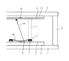
図1に示されるように、本例の表示パネルは、第1の基板であるリアプレート1と、第2の基板であるフェースプレート2を間隔をあけて対向させ、両者間に板状のスペーサ3を挟み込むと共に、周囲を側壁4で封止し、内部を真空雰囲気としたものとなっている。
As shown in FIG. 1, the display panel of the present example has a
リアプレート1上には、行方向配線5、列方向配線6、電極間絶縁層7(図2、図4参照)および電子放出素子8を形成した電子源基板9が固定されている。
On the
図示される電子放出素子8は、一対の素子電極間に電子放出部を有する導電性薄膜が接続された表面伝導型電子放出素子である。本例は、この表面伝導型電子放出素子をN×M個配置し、それぞれ等間隔で形成したM本の行方向配線5とN本の列方向配線6でマトリクス配線したマルチ電子ビーム源を有するものとなっている。また、本例においては、行方向配線5が電極間絶縁層7を介して列方向配線6上に位置しており、しかも行方向配線5には引出端子Dx1〜Dxmを介して走査信号が印加され、列方向配線6には引出端子Dy1〜Dynを介して変調信号(画像信号)が印加されるものとなっている。
The illustrated electron-emitting
行方向配線5および列方向配線電極6は、銀ペーストをスクリーン印刷法により塗布することで形成することができる。また、例えばフォトリソグラフィ法を用いて形成することもできる。
The row wirings 5 and the
行方向配線5および列方向配線電極6の構成材料としては、上記銀ペーストの他に、各種導電材料を適用することができる。例えば、スクリーン印刷法を用いて行方向配線5および列方向配線電極6を形成する場合には、金属とガラスペーストと混合させた塗布材料を用いることができ、めっき法を用いて金属を析出させることで行方向配線5および列方向配線電極6を形成する場合には、めっき浴材料を適用することができる。
As a constituent material of the row-
フェースプレート2の下面(リアプレート1との対向面)には、蛍光膜10が形成されている。本例の表示パネルはカラ−表示であるため、蛍光膜10は赤、緑、青の3原色の蛍光体が塗り分けられている。各色の蛍光体は、例えばストライプ状に塗り分けられており、各色の蛍光体のストライプの間には黒色の導電体(ブラックストライプ)が設けられている。黒色の導電体を設ける目的は、電子ビ−ムの照射位置に多少のずれがあっても表示色にずれが生じないようにすること、外光の反射を防止して表示コントラストの低下を防ぐこと、電子ビ−ムによる蛍光膜のチャ−ジアップを防止することなどである。黒色の導電体としては、黒鉛を主成分とした材料を用いることができるが、上記の目的に適するものであればこれ以外の材料を用いることもできる。また、3原色の蛍光体の塗り分け方は、上記ストライプ状だけでなく、例えばデルタ状配列や、それ以外の配列とすることもできる。
A
上記蛍光膜10の表面には、フェースプレート2に設けられた導電性部材であるメタルバック(加速電極)11が設けられている。このメタルバック11は、電子放出素子8から放出される電子を加速して引き上げるためのもので、高圧端子Hvから高電圧が印加され、前記行方向配線5に比して高電位に規定されるものとなっている。本例のような表面伝導型電子放出素子を用いた表示パネルの場合、通常、行方向配線5とメタルバック11間には5〜20KV程度の電位差が形成される。
On the surface of the
行方向配線5上には、行方向配線5と平行に、板状のスペーサ3が取り付けられている。このスペーサ3は、行方向配線5上に乗せられた状態で、両端がスペーサ固定ブロック12に取り付けられて支持されている。スペーサ固定ブロック12を用いてスペーサ3を固定することで、電子の運動エネルギーが小さく、電子軌道が電場の影響を受けやすい電子放出素子8近傍の電場の乱れを小さくすることができる。
On the
スペーサ3は、表示パネルに耐大気圧性を持たせるために、通常、等間隔で複数設けられ、電子放出素子8、これを駆動するための行方向配線5および列方向配線6が設けられた電子源基板9を有するリアプレート1と、蛍光膜10およびメタルバック11が設けられたフェースプレート2との間に挟み込まれ、上下面がメタルバック11と行方向配線5にそれぞれ圧接されている。また、リアプレート1とフェースプレート2の周縁部には、側壁4が挟み込まれており、リアプレート1と側壁4の接合部およびフェースプレート2と側壁4の接合部は、それぞれフリットガラスなどによって封止されている。
A plurality of
さらにスペーサ3について説明すると、スペーサ3は、リアプレート1側の行方向配線5および列方向配線6とフェースプレート2側のメタルバック11との間に印加される高電圧に耐えるだけの絶縁性を有し、かつスペーサ3の表面への帯電を防止する程度の導電性を有する。スペーサ3は、図4に示されるように、絶縁性材料で構成された基体13と、その表面を被覆する高抵抗膜14で構成されている。
Further, the
スペーサ3の基体13の構成材料としては、例えば石英ガラス、Naなどの不純物含有量を減少したガラス、ソーダライムガラス、アルミナなどのセラミックスなどが挙げられる。この基体13の構成材料は、その熱膨張率が、電子源基板9、リアプレート1、フェイスプレート2などの構成材料と同一または近いものが好ましい。
Examples of the constituent material of the
スペーサ3の表面を被覆する高抵抗膜14には、高電位側となるメタルバック11に印加される加速電圧Vaを高抵抗膜14の抵抗値で除した電流が流され、これによってスペーサ3表面への帯電が防止される。このため、高抵抗膜14の抵抗値は、帯電および消費電力からその望ましい範囲に設定される。高抵抗膜14のシート抵抗は、帯電防止の観点からすると、1014Ω/□以下が好ましく、1012Ω/□以下であることがより好ましく、1011Ω/□以下であることが最も好ましい。高抵抗膜14のシート抵抗の下限は、スペーサ3形状とスペーサ3間に印加される電圧により左右されるが、消費電力を抑制するために、105Ω/□以上であることが好ましく、107Ω/□以上であることがより好ましい。
A current obtained by dividing the acceleration voltage Va applied to the metal back 11 on the high potential side by the resistance value of the high-
高抵抗膜14を構成する材料の表面エネルギーおよび基体13との密着性や基体13の温度によっても異なるが、一般的に10nm以下の薄膜は島状に形成され、抵抗が不安定で再現性に乏しい。一方、膜厚が1μm以上では膜応力が大きくなって膜はがれの危険性が高まり、かつ成膜時間が長くなるため生産性が悪い。従って、基体13上に形成する高抵抗膜14の厚みは10nm〜1μmの範囲が好ましい。より好ましくは、膜厚は50〜500nmである。シート抵抗はρ/t(ρ:比抵抗、t:膜厚)であり、前記シート抵抗と膜厚の好ましい範囲から、高抵抗膜14の比抵抗ρは0.1〜108Ωcmであることが好ましい。さらにシート抵抗と膜厚のより好ましい範囲を実現するためには、比抵抗ρは102〜106Ωcmとするのが好ましい。
Although it depends on the surface energy of the material constituting the high-
スペーサ3は、前記のように、その表面に形成した高抵抗膜14に電流が流れることや、表示パネル全体が動作中に発熱することにより、その温度が上昇する。高抵抗膜14の抵抗温度係数が大きな負の値であると、温度が上昇した時に抵抗値が減少し、高抵抗膜14に流れる電流が増加し、さらなる温度上昇をもたらすことになる。そして、電流は電源の限界を越えるまで増加し続ける。このような電流の暴走が発生する抵抗温度係数の値は、経験的に、負の値でしかも絶対値が1%以上である。すなわち、高抵抗膜14の抵抗温度係数は、−1%より大きい値であることが好ましい。
As described above, the temperature of the
高抵抗膜14の構成材料としては、例えば金属酸化物を用いることができる。金属酸化物の中でも、クロム、ニッケル、銅の酸化物が好ましい。その理由は、これらの酸化物は二次電子放出効率が比較的小さく、電子放出素子8から放出された電子がスペーサ3に当たっても帯電しにくいことにある。これらの金属酸化物以外では、炭素は二次電子放出効率が小さく、好ましい材料である。特に、非晶質カーボンは高抵抗であるため、適切なスペーサ3の表面抵抗が得やすい。
As a constituent material of the
高抵抗膜14の他の構成材料として、アルミニウムと遷移金属の合金の窒化物は、遷移金属の組成を調整することにより、良導電体から絶縁体まで広い範囲に抵抗値を制御できると共に、表示パネルの製造工程における抵抗値の変化が少なく、安定していることから、好適な材料である。遷移金属元素としては、Ti、Cr、Taなどを挙げることができる。
As another constituent material of the high-
上記合金窒化物膜は、窒素ガス雰囲気を利用した、スパッタ、電子ビーム蒸着、イオンプレーテイング、イオンアシスト蒸着法などの薄膜形成手法により形成することができる。前記金属酸化物膜は、酸素ガス雰囲気を利用した薄膜形成手法で形成することができる。その他、CVD法、アルコキシド塗布法でも金属酸化膜を形成することができる。カーボン膜は、蒸着法、スパッタ法、CVD法、プラズマCVD法で作製され、特に非晶質カーボン膜は、成膜中の雰囲気に水素が含まれるようにするか、成膜ガスに炭化水素ガスを使用することで得ることができる。 The alloy nitride film can be formed by a thin film forming technique such as sputtering, electron beam evaporation, ion plating, or ion-assisted evaporation using a nitrogen gas atmosphere. The metal oxide film can be formed by a thin film formation technique using an oxygen gas atmosphere. Alternatively, a metal oxide film can be formed by a CVD method or an alkoxide coating method. The carbon film is formed by a vapor deposition method, a sputtering method, a CVD method, or a plasma CVD method. In particular, an amorphous carbon film is made so that hydrogen is contained in an atmosphere during film formation or a hydrocarbon gas is used as a film formation gas. Can be obtained by using
スペーサ3は、前記のように、リアプレート1とフェースプレート2間に挟み込まれており、その表面を被覆している高抵抗膜14は、リアプレート1側の配線(本例では行方向配線5)と、フェースプレート2側の導電性部材(本例ではメタルバック11)とに圧接され、それぞれ電気的に接続されている。特に行方向配線5との電気的接続は、図2に示されるように、行方向配線5の列方向配線6との交差部が他の箇所に比して列方向配線6の厚み分だけフェースプレート2側に突出していることから、当該部分と高抵抗膜14が接触することで行われている。すなわち、高抵抗膜14と行方向配線5の電気的接続は、図3に示されるように、行方向配線5の列方向配線6との交差部が接触部15、それ以外の箇所が非接触部16となることで、当該交差部の間隔で行われている。このときのスペーサ3表面におけるリアプレート1近傍の等電位線17を模式的に図2に太線で示す。
The
図2に示される等電位線17および図3から分かるように、非接触部16にも高抵抗膜14が存在するため、非接触部16近傍の電位が持ち上がる。これは、メタルバック11から接触部15へと流れる電流の経路のうち、非接触部16を介する電流経路の抵抗値の方が、非接触部16を介さない電流経路(例えば、接触部15の直上部分からの電流経路)の抵抗値より大きいため、この増加抵抗値による電圧降下分だけ電位が持ち上がるために生じる。
As can be seen from the
また、図1および図2に示されるように、列方向配線6は等間隔であることから、上記接触部15と非接触部16は等間隔で形成されており、しかも電子放出素子8は、図1から明らかなように、行方向配線5と列方向配線6の間にあることから、スペーサ3に隣接する電子放出素子8は総て非接触部16に隣接する位置にあり、この電子放出素子8から放出される電子ビームは、総て非接触部16に対応するスペーサ3の表面電位の影響を等しく受けるものとなっている。
As shown in FIGS. 1 and 2, since the column-
図4に模式的に示されるように、本例における電子放出素子8は、スペーサ3に隣接するものを除いて行方向配線5間のほぼ中央に設けられているが、スペーサ3に隣接する電子放出素子8は、距離Lだけスペーサ3側に近付けて設けられている。この距離Lをオフセットという。また、図4に破線で示される電子ビーム軌道18のように、電子放出素子8から放出される電子は、(1)電子放出素子8の電子放出部近傍ではスペーサ3から遠ざかるように飛翔し、(2)スペーサ3の底面近傍に対応する位置では逆にスペーサ3に近付くように飛翔し、最終的に所望の所定照射位置19に到達している。ここで、所望照射位置とは、複数配列形成された電子放出素子の各々から放出された電子ビームの照射位置が、互いに略等間隔となる位置を意味し、上記図4の形態では、隣接する行方向配線間の略中心に対応する位置のフェースプレート部分に想到する。所定照射位置19に電子ビームが到達する理由を以下に詳しく説明する。
As schematically shown in FIG. 4, the electron-emitting
電子放出部近傍
行方向配線5と列方向配線6は、メタルバック11に印加される電子ビーム加速用の電圧と比較するとほぼ同電位(0V)とみることができる。高抵抗膜14と行方向配線5の接触部15(図3参照)が電子放出素子8よりも上方(フェースプレート2側)にあるため、図4に示されるように、電子放出素子8上方の等電位線20は、電子放出素子8の電子放出部近傍では下に凸の曲線となる。電子放出素子8がスペーサ3側に片寄った位置になく、行方向配線5間のほぼ中央である場合は、電位分布の対称性により電子ビームはほぼ垂直な軌道をとるが、本例のようにスペーサ3に近付いていると、電位分布が非対称となり、スペーサ3から遠ざかるような軌道をとる。
The row-
スペーサ3に隣接する電子放出素子8をオフセットLをとらずに、行方向配線5間のほぼ中央に設けた場合の電子ビーム軌道18を図5に示す。また、スペーサ3を取り除いた状態で、電子放出素子8をオフセットL(行方向配線5間の中央から電子放出素子8の電子放出部までの距離)だけ一方の行方向配線5側に近付けた場合の電子ビーム軌道18を図6に示す。
FIG. 5 shows an
スペーサ3から遠ざかる成分はオフセットLの関数であり、本例ではオフセットLが大きくなるほど(電子放出素子8がスペーサ3に近づくほど)電子ビーム軌道18はスペーサ3から遠ざかることになる。オフセットLと、電子ビームが到達する位置のスペーサー3からの距離との関係を図7に示す。
The component moving away from the
スペーサ3の底面近傍対応位置
図2および図3で説明したように、スペーサ3の高抵抗膜14が、列方向配線6との交差部毎に行方向配線5と接触している結果、図3に示す非接触部16の電位が上昇し、図4に示すように、スペーサ3の底面近傍に対応する上に凸の等電位線20を生じ、電子ビームはスペーサ3に近付くように飛翔する。
As described with reference to FIGS. 2 and 3, the
スペーサ3に近付く成分は、高抵抗膜14と行方向配線5の接触状態によって決まる接触部15(図3参照)の面積(接触面積)Sの関数であり、その様子をあらわしたのが図8である。図8に示されるように、接触面積Sが大きくなるほど電子ビームはスペーサから遠ざかる。
The component approaching the
高抵抗膜14と行方向配線5の接触状態は、上記面積Sだけでなく、他にも様々なパラメータで表すことができる。例えば図3に示される接触部15の周囲長、行方向配線5の幅方向の非接触部16の長さGy、行方向配線5の長さ方向の隣接接触部15間距離Gxなどの関数としても表すことができる。接触部15の周囲長が小さくなればなるほど、Gx、Gyが大きくなればなるほど、電子ビームはスペーサ3に近付く。
The contact state between the
以上の説明より、オフセットLや、高抵抗膜14と行方向配線5の接触状態(例えば接触面積S)という、スペーサ3自体とは関係しない別個の独立なパラメータによって電子ビームの到達位置を制御できることが分かる。
According to the above description, the arrival position of the electron beam can be controlled by the independent parameters independent of the
図9は、縦軸にオフセットL、横軸に接触面積Sをとり、電子ビームが所定照射位置19(図4参照)に到達するオフセットLと接触部面積Sの関係を示す曲線を表したものである。 FIG. 9 shows a curve representing the relationship between the offset L at which the electron beam reaches the predetermined irradiation position 19 (see FIG. 4) and the contact area S, with the offset L on the vertical axis and the contact area S on the horizontal axis. It is.
図9から分かるとおり、電子ビームが所定照射位置19に到達するずれの無い条件は複数存在し、例えば図9のA点の条件でもB点の条件でも設計できる。A点の条件に比してオフセットLが大きく、接触面積Sが小さいB点の条件で設計する場合、例えば行方向配線5を蒲鉾断面形状とし、行方向配線5の上面を平面ではなく、曲面とすることで、接触面積Sを小さくすることができる。
As can be seen from FIG. 9, there are a plurality of conditions under which the electron beam does not reach the
実際の設計では、例えば静電界計算と電子ビーム軌道シミュレーションから、所定照射位置19に到達するオフセットLと接触状態(例えば接触面積S)を決定する。また、実測データに基づく条件決定も可能である。
In an actual design, an offset L reaching the
以上説明してきた通り、本発明によれば、スペーサ3自体の構成によらず、高抵抗膜14と行方向配線5の接触状態やオフセットLを制御することで所望の電子ビーム到達位置を達成することができる。このため、本発明によれば、同一構成のスペーサ3で、様々な画像形成装置に対応可能である。例えば高精細化のために画素ピッチを変更したり、高輝度化のために加速電圧を高くしたりすることに基づく仕様変更の場合でも、スペーサ3自体は同一のものを用い、上記高抵抗膜14と行方向配線5の接触状態やオフセットLの変更で対応することができる。従って、本発明によれば、生産性を著しく向上させ、コストの大幅な削減に結び付けることができる。
As described above, according to the present invention, a desired electron beam arrival position is achieved by controlling the contact state and offset L between the high-
本例で説明した表示パネルにつき、スペーサ3の基材として、旭ガラス(株)製のPD200を用い、高抵抗膜14として窒化タングステン・ゲルマニム合金化合物(WGeN)を、タングステンターゲットとゲルマニウムターゲットを窒素ガス中で、同時スパッタリングして成膜した。このときスペーサ3の基体13を回転させながら成膜することで、表面全面にわたり膜厚は200Å、シート抵抗は2.5×10¹²Ω/□であった。
For the display panel described in this example, a PD200 manufactured by Asahi Glass Co., Ltd. was used as a base material of the
また、スペーサ3の総厚を300μm、スペーサー3の総高さを2.4mm、列方向配線6間の間隔(当接点の間隔)を300μm、行方向配線5間の間隔を920μm、行方向配線5の幅を690μm、電子放出素子8の電子放出部から行方向配線5の上面までの高さを75μmとし、メタルバック11への印加電圧を15KV、行方向配線5と列方向配線6間への印加電圧は14Vとした場合の面積SとオフセットLとの関係を表1に示す。なお、表1における条件A,Bは、図9における点A,Bに対応する。
The total thickness of the

(第2の例)
本発明の第2の例について、第1の例と違う点のみ説明する。
(Second example)
In the second example of the present invention, only the differences from the first example will be described.
図10、図11、図13は第1の例の図2、図3、図4に対応する図で、本例と第1の例との違いは、列方向配線6との交差位置の行方向配線5上に導電性台部21を有する点である。このような構成にすることで接触状態を安定させ、電子ビーム到達位置を精度よく制御することができる。
FIGS. 10, 11, and 13 correspond to FIGS. 2, 3, and 4 of the first example. The difference between the present example and the first example is that the row at the intersection position with the column-
導電性台部21は、行方向配線5を形成した後、行方向配線5と同様の方法で行方向配線5上に形成することができる。また、この導電性台部21は、総ての行方向配線5に一括して形成してもよいが、スペーサ3が当接される行方向配線5にのみ形成してもよい。
After forming the
導電性台部21は、スペーサ3の基体13よりも堅い材料で形成することが好ましい。例えば、スペーサ3をガラスを基体13として形成し、導電性台部21をこのガラスよりもヤング率の小さい導電性セラミックスで構成することが挙げられる。この場合、導電性台部21の変形がより小さくなることで、個々の接触部15の形状や位置などのばらつきが少なくなり、電子ビーム到達位置の更なる精度向上が望める。尚、導電性台部を設けた場合に限らず、配線とスペーサが直接接する場合は、配線をスペーサのガラス基体よりも硬くすれば(ヤング率を小さくすれば)、同様の効果が得られる。
The
(第3の例)
本発明の第3の例について、第2の例と違う点のみ説明する。
(Third example)
In the third example of the present invention, only the points different from the second example will be described.
導電性台部21の配置場所は、必ずしも第2の例のように、行方向配線5の列方向配線6と交差する部分上である必要はない。本例においては、図13に示されるように、第2の例の1/2のピッチで導電性台部21が配置されている。
The disposition location of the
第2の例と同様に、導電性台部21はスペーサ3の基体13よりも堅い部材で形成することが好ましい。また、本例のように導電性台部21を配置することで、接触面設計の自由度が大きくなるという利点がある。
As in the second example, the
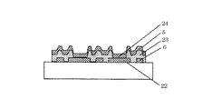
列方向配線6と行方向配線5との交差部以外でスペーサ3と行方向配線5を接触させることは、列方向配線6を形成しない領域に接触点形成用の下地を設けることによっても可能である。以下にその一例を示す。
The contact between the
図14はこの形態の概要を示す部分拡大図であり、図15は、図14のA−A断面図である。 FIG. 14 is a partially enlarged view showing an outline of this embodiment, and FIG. 15 is a sectional view taken along line AA of FIG.
図14および図15に示すとおり、部分電極22を設け、これを絶縁層23に設けられたコンタクトホール24を介して行方向配線5に接続すると共に、部分電極22に、列方向配線6に接続された素子電極25と向き合うもう一つの素子電極26を接続しておくことで、部分電極22とコンタクトホール24による段差を利用して、スペーサ3(図13参照)と行方向配線5の接触部を増やすことができる(行方向配線5の凸部を増やすことができる)。
As shown in FIGS. 14 and 15, a
この構成の具体的製造方法を図16(a)〜(d)を用いて説明する。 A specific manufacturing method of this configuration will be described with reference to FIGS.
まず、図16(a)に示すよう、素子電極25,26を形成した後、図16(b)に示すように、部分電極22および列方向配線6を一括形成し、図16(c)に示すように、この部分電極22と列方向配線6の一部の上に絶縁層23を形成した後、部分電極22上の絶縁層23を部分電極22より一回り小さい形で除去してコンタクトホール24を形成し、さらに図16(d)に示すように、絶縁層23上に行方向配線5を形成し、コンタクトホール24(図16(c)参照)を介して部分電極22に接続する。このようにして形成された行方向配線5上に、スペーサ3(図13参照)を配置することによって、列方向配線6と行方向配線5との交差部以外にもスペーサ3と行方向配線5の接触部が得られる構成を実現することができる。
First, as shown in FIG. 16A, after forming the
(第4の例)
本発明の第4の例について、第1の例と違う点のみ説明する。
(Fourth example)
In the fourth example of the present invention, only the differences from the first example will be described.
図17および図18は第1の例についての図4および図5に対応する図で、図示されるように、本例におけるスペーサ3と行方向配線5の接触面は低い位置にあり、実質的に電子放出素子8の電子放出部と同一平面にある。このため、図17に示される通り、等電位線20として、図4に示されるような下に凸な形状のものがないか、非常に小さいため、オフセットLと電子ビーム到達位置の関係は、第1の例と反対の傾向を示す。
17 and 18 are views corresponding to FIGS. 4 and 5 for the first example. As shown, the contact surface between the
すなわち、電子放出素子8がスペーサに近づくほど、電子ビームはスペーサ3に近づく。さらにスペーサ3と行方向配線5の接触面の高さよりも、電子放出素子8の電子放出部のほうが高い場合も同様の傾向で、電子放出素子8がスペーサ3に近づくほど、電子ビームはスペーサ3に近づく。
That is, the electron beam approaches the
図17に示されるように、オフセットLだけスペーサ3から離れる位置に配置された電子放出素子8から放出された電子ビームは、ゆがんだ等電位線20によりスペーサ3に近づくように飛翔し、所望の電子ビーム到達位置を得る。ゆがんだ等電位線20ができるのは、第1の例で説明した通り、高抵抗膜14と行方向配線5の部分的な接触によるものである。また、スペーサ3を取り除いた状態で、電子放出素子8をオフセットLだけ一方の行方向配線5側に近付けた場合の電子ビーム軌道18を図18に示す。
As shown in FIG. 17, the electron beam emitted from the electron-emitting
以上のように、表示パネルの大きな設計変更の際にも本発明を適用することで電子ビームずれの無い画像形成装置を実現することができる。 As described above, by applying the present invention even when the design of the display panel is largely changed, it is possible to realize an image forming apparatus having no electron beam deviation.
(第5の例)
本発明の第5の例について、第1の例と違う点のみ説明する。
(Fifth example)
In the fifth example of the present invention, only the differences from the first example will be described.
本例は、スペーサ3の接触制御をフェースプレート2側に適用した例である。
This example is an example in which the contact control of the
図19および図20は、第1の例の図2および図4に対応するもので、本例においては、フェースプレート2側に導電性台部21を設け、これによって図3で説明した接触部15と非接触部16をフェースプレート2側にも形成して電位分布を制御し、所望の電子ビーム到達位置を達成しているものである。
FIGS. 19 and 20 correspond to FIGS. 2 and 4 of the first example. In the present example, a
具体的には、図20に示されるように、(1)電子放出素子8の電子放出部近傍で電子ビームをスペーサ3から遠ざけ、(2)スペーサ3の行方向配線5との接触面近傍の高さの位置でスペーサ3に近付け、(3)スペーサ3のメタルバック11との接触面近傍で再びスペーサ3から遠ざけることで、所望の電子ビーム軌道18を得ているものである。
Specifically, as shown in FIG. 20, (1) the electron beam is moved away from the
本例では、導電性台部21を用いる構成にしたが、例えば前述の黒色の導電体(ブラックストライプ)をフェースプレート2側で接触する導電性部材として用いるような構成にしてもよい。また、フェースプレート2側の接触制御においても、第1の例〜第3の例で述べたリアプレート1側における接触制御の考えを適用することができる。
In this example, the
具体的には、スペーサ3のフェースプレート2側接触面近傍で電子ビーム軌道18を遠ざける成分は、高抵抗膜14とフェースプレート2側の導電性台部21の接触状態の関数、例えば接触面積Sの関数であり、接触面積Sが小さいほど電子ビームはスペーサ3から遠ざかる。また、導電性台部21はスペーサ3の基体13より堅いと電子ビーム位置の精密制御に有利であり、さらに導電性台部21は任意の場所に配置設計することができる。
Specifically, a component that keeps the
また、以上の例においては、スペーサ3の高抵抗膜14は、リアプレート1側では行方向配線5に接触させているが、列方向配線6が表面に露出するようにした場合には、列方向配線6に接触させるようにすることもできる。
Further, in the above example, the
1 リアプレート
2 フェースプレート
3 スペーサ
4 側壁
5 行方向配線
6 列方向配線
7 電極間絶縁層
8 電子放出素子
9 電子源基板
10 蛍光膜
11 メタルバック
12 スペーサー固定ブロック
13 基体
14 高抵抗膜
15 接触部
16 非接触部
17 等電位線
18 電子ビーム軌道
19 所定照射位置
20 等電位線
21 導電性台部
22 部分電極
23 絶縁層
24 コンタクトホール
25 素子電極
26 素子電極
DESCRIPTION OF
Claims (8)
前記スペーサの高抵抗膜と前記配線との電気的接続のための接触部分が前記配線の長さ方向に沿って所定間隔で設けられていることを特徴とする画像形成装置。 A first substrate having a plurality of electron-emitting devices and a wiring for driving the plurality of electron-emitting devices; and a conductive member arranged to face the first substrate and having a higher potential than the wiring. A second substrate having a higher resistance than the wiring disposed between the first substrate and the second substrate along the wiring and electrically connected to the wiring and the conductive member. An image forming apparatus having a plate-like spacer covered with a film,
An image forming apparatus, wherein contact portions for electrical connection between the high resistance film of the spacer and the wiring are provided at predetermined intervals along the length direction of the wiring.
Priority Applications (1)
| Application Number | Priority Date | Filing Date | Title |
|---|---|---|---|
| JP2004139393A JP3840233B2 (en) | 2003-05-15 | 2004-05-10 | Image forming apparatus |
Applications Claiming Priority (2)
| Application Number | Priority Date | Filing Date | Title |
|---|---|---|---|
| JP2003136741 | 2003-05-15 | ||
| JP2004139393A JP3840233B2 (en) | 2003-05-15 | 2004-05-10 | Image forming apparatus |
Publications (3)
| Publication Number | Publication Date |
|---|---|
| JP2004363094A true JP2004363094A (en) | 2004-12-24 |
| JP2004363094A5 JP2004363094A5 (en) | 2006-01-05 |
| JP3840233B2 JP3840233B2 (en) | 2006-11-01 |
Family
ID=34067245
Family Applications (1)
| Application Number | Title | Priority Date | Filing Date |
|---|---|---|---|
| JP2004139393A Expired - Fee Related JP3840233B2 (en) | 2003-05-15 | 2004-05-10 | Image forming apparatus |
Country Status (1)
| Country | Link |
|---|---|
| JP (1) | JP3840233B2 (en) |
Cited By (1)
| Publication number | Priority date | Publication date | Assignee | Title |
|---|---|---|---|---|
| WO2006070613A1 (en) * | 2004-12-27 | 2006-07-06 | Kabushiki Kaisha Toshiba | Image display device |
-
2004
- 2004-05-10 JP JP2004139393A patent/JP3840233B2/en not_active Expired - Fee Related
Cited By (4)
| Publication number | Priority date | Publication date | Assignee | Title |
|---|---|---|---|---|
| WO2006070613A1 (en) * | 2004-12-27 | 2006-07-06 | Kabushiki Kaisha Toshiba | Image display device |
| JP2006185723A (en) * | 2004-12-27 | 2006-07-13 | Toshiba Corp | Image display device |
| US7692370B2 (en) | 2004-12-27 | 2010-04-06 | Canon Kabushiki Kaisha | Image display apparatus |
| JP4594076B2 (en) * | 2004-12-27 | 2010-12-08 | キヤノン株式会社 | Image display device |
Also Published As
| Publication number | Publication date |
|---|---|
| JP3840233B2 (en) | 2006-11-01 |
Similar Documents
| Publication | Publication Date | Title |
|---|---|---|
| US7449828B2 (en) | Image forming apparatus provided with resistive-coated spacers contacting protruding sections of wiring elements | |
| JP2010262936A (en) | Electron beam device | |
| JP3507392B2 (en) | Electron beam equipment | |
| KR20060046343A (en) | Image display apparatus | |
| JP2002237268A (en) | Image forming device | |
| US7548017B2 (en) | Surface conduction electron emitter display | |
| JP4481891B2 (en) | Image display device | |
| JP2006019247A (en) | Image display apparatus | |
| KR100661009B1 (en) | Image forming device and a television apparatus having the same | |
| JP3840233B2 (en) | Image forming apparatus | |
| JP4481892B2 (en) | Image display device | |
| JP3944219B2 (en) | Image display device | |
| JP4773812B2 (en) | Manufacturing method of spacer | |
| JP4036417B2 (en) | Image forming apparatus | |
| JP3762414B2 (en) | Electron beam equipment | |
| JP2005209376A (en) | Image formation device | |
| JP3891585B2 (en) | Electron beam apparatus, image display apparatus, and television apparatus | |
| US20080136306A1 (en) | Flat panel display and spacer for use therein | |
| JP2004079359A (en) | Electron beam device and its spacer | |
| JP2007207739A (en) | Image displaying apparatus | |
| JP2000340142A (en) | Electron-beam device and image forming device using the same |
Legal Events
| Date | Code | Title | Description |
|---|---|---|---|
| A621 | Written request for application examination |
Effective date: 20041027 Free format text: JAPANESE INTERMEDIATE CODE: A621 |
|
| A521 | Written amendment |
Effective date: 20051115 Free format text: JAPANESE INTERMEDIATE CODE: A523 |
|
| A977 | Report on retrieval |
Free format text: JAPANESE INTERMEDIATE CODE: A971007 Effective date: 20051222 |
|
| A131 | Notification of reasons for refusal |
Effective date: 20060328 Free format text: JAPANESE INTERMEDIATE CODE: A131 |
|
| A521 | Written amendment |
Free format text: JAPANESE INTERMEDIATE CODE: A523 Effective date: 20060405 |
|
| TRDD | Decision of grant or rejection written | ||
| A01 | Written decision to grant a patent or to grant a registration (utility model) |
Free format text: JAPANESE INTERMEDIATE CODE: A01 Effective date: 20060718 |
|
| A61 | First payment of annual fees (during grant procedure) |
Free format text: JAPANESE INTERMEDIATE CODE: A61 Effective date: 20060804 |
|
| R150 | Certificate of patent (=grant) or registration of utility model |
Free format text: JAPANESE INTERMEDIATE CODE: R150 |
|
| FPAY | Renewal fee payment (prs date is renewal date of database) |
Year of fee payment: 3 Free format text: PAYMENT UNTIL: 20090811 |
|
| FPAY | Renewal fee payment (prs date is renewal date of database) |
Free format text: PAYMENT UNTIL: 20100811 Year of fee payment: 4 |
|
| FPAY | Renewal fee payment (prs date is renewal date of database) |
Year of fee payment: 5 Free format text: PAYMENT UNTIL: 20110811 |
|
| FPAY | Renewal fee payment (prs date is renewal date of database) |
Free format text: PAYMENT UNTIL: 20120811 Year of fee payment: 6 |
|
| FPAY | Renewal fee payment (prs date is renewal date of database) |
Year of fee payment: 6 Free format text: PAYMENT UNTIL: 20120811 |
|
| FPAY | Renewal fee payment (prs date is renewal date of database) |
Free format text: PAYMENT UNTIL: 20130811 Year of fee payment: 7 |
|
| LAPS | Cancellation because of no payment of annual fees |