JP2004362600A - Memory control device and memory system - Google Patents
Memory control device and memory system Download PDFInfo
- Publication number
- JP2004362600A JP2004362600A JP2004212455A JP2004212455A JP2004362600A JP 2004362600 A JP2004362600 A JP 2004362600A JP 2004212455 A JP2004212455 A JP 2004212455A JP 2004212455 A JP2004212455 A JP 2004212455A JP 2004362600 A JP2004362600 A JP 2004362600A
- Authority
- JP
- Japan
- Prior art keywords
- storage
- level device
- frame
- port
- access
- Prior art date
- Legal status (The legal status is an assumption and is not a legal conclusion. Google has not performed a legal analysis and makes no representation as to the accuracy of the status listed.)
- Pending
Links
Images


Abstract
Description
本発明は、上位装置と接続される記憶制御装置、及び記憶制御装置配下の記憶装置から成る記憶システムにおいて、上位装置から記憶制御装置配下の記憶装置へのアクセス要求があった際の、不正アクセス防止手段に関する。 The present invention is directed to a storage system including a storage control device connected to a higher-level device and a storage device under the storage control device. Regarding prevention means.
ネットワーク上の不正アクセス防止に関しては、従来から種々の技術が知られている。
例えば、特開平3−152652号公報には、TCP/IPをサポートするコンピュータシステム間のネットワークセキュリティシステムとして、ログインできるユーザIDをメモリに定義しておくことにより、定義されたユーザID以外でログインしようとすると、そのネットワークを切断する機能を持たせることが開示されている。
また、特開昭63−253450号公報には、中央処理装置のオペレーティングシステムがユーザID、パスワード、回線アドレスをチェックすることにより、ディスク装置のファイルへの不正アクセス防止を行なうことが示されている。
さらに、IBM社のESCONインタフェースでは、上位装置が当該上位装置の論理アドレスをソースアドレスとしてフレームに格納し、送信してくることを利用して、記憶制御装置が事前に記憶制御装置に設定した論理アドレスとフレーム内の論理アドレスが一致するか否かをチェックする機能を設けている。
上述した従来技術は、上位論理層に1種類のレイヤを搭載するインタフェースを対象とした不正アクセス防止手段の域を出ないものである。
しかし、ANSIX3T11で標準化されたファイバチャネルは、ネットワーク形アーキテクチャであり、上位論理層にはTCP/IP、SCSI、ESCON、IPI等の種々のレイヤを搭載可能である。すなわち、データのフォーマットや内容には無関係に一台の装置から別の装置へバッファの内容を移すため、他のインタフェースと論理的に互換性を持ち、物理的に自由にアクセス可能である。特に、このファイバチャネルと、ディスクアレイ装置等の複数の記憶領域を有する記憶装置とを備えた記憶システムにおいては、上記記憶領域は多くの上位装置に共用される。したがって、従来の不正アクセス防止策では不十分であり、ユーザが意識したセキュリティ設定により、機密保持を行なう必要がある。
Various techniques have been known for preventing unauthorized access on a network.
For example, Japanese Patent Laid-Open Publication No. Hei 3-152652 discloses a network security system between computer systems supporting TCP / IP, in which a user ID that can log in is defined in a memory so that a user can log in with a user ID other than the defined user ID. Then, it is disclosed that a function of disconnecting the network is provided.
Japanese Patent Application Laid-Open No. 63-253450 discloses that an operating system of a central processing unit checks a user ID, a password, and a line address to prevent unauthorized access to a file on a disk device. .
Further, in the IBM company's ESCON interface, the storage controller stores the logical address of the host as a source address in a frame and transmits the frame, and the storage controller uses the logical address previously set in the storage controller. A function is provided for checking whether the address matches the logical address in the frame.
The above-described prior art does not go beyond the area of the unauthorized access prevention means for an interface having one type of layer mounted on the upper logical layer.
However, Fiber Channel standardized by ANSIX3T11 has a network type architecture, and various layers such as TCP / IP, SCSI, ESCON, and IPI can be mounted on an upper logical layer. That is, since the contents of the buffer are transferred from one device to another regardless of the format and contents of the data, they are logically compatible with other interfaces and can be freely accessed physically. In particular, in a storage system including this fiber channel and a storage device having a plurality of storage regions such as a disk array device, the storage region is shared by many higher-level devices. Therefore, the conventional measures for preventing unauthorized access are not sufficient, and it is necessary to maintain confidentiality by security settings conscious of the user.
本発明は、ANSIX3T11で標準化されたファイバチャネルを、上位装置と記憶制御装置間のインタフェースとし、上位装置、記憶制御装置、及び、この記憶制御装置配下の記憶装置から成るコンピュータシステムにおいて、物理的にあらゆる上位装置からのアクセスを受け付けることが可能な環境の中で、上位装置からの不正なアクセスを拒絶する手段を持たなかった記憶制御装置に対し、上位装置からの不正なアクセスを防止するセキュリティ機能を設定出来る記憶制御装置及び記憶システムを提供することを目的とする。 According to the present invention, a fiber channel standardized by ANIX3T11 is used as an interface between a host device and a storage control device. In a computer system including a host device, a storage control device, and a storage device under the storage control device, a physical system is physically used. A security function that prevents unauthorized access from a host device to a storage control device that does not have a means to reject unauthorized access from the host device in an environment that can accept access from any host device. It is an object of the present invention to provide a storage control device and a storage system capable of setting the following.
さらに、本発明は、上位装置からの不正アクセス防止のために、アクセス可能な上位装置を容易に設定できる方式を持つ記憶制御装置及び記憶システムを提供することを目的とする。 Still another object of the present invention is to provide a storage control device and a storage system having a method of easily setting an accessible higher-level device for preventing unauthorized access from a higher-level device.
本発明によれば、上記目的は、アクセス可能な上位装置の、上位装置を一意に識別するN_Port_Name情報を当該記憶制御装置に設定し、上位装置から送られてくるフレーム内に格納されたN_Port_Name情報と比較し、アクセスの可否を決定することにより達成される。 According to the present invention, the object is to set N_Port_Name information for uniquely identifying an upper-level device of an accessible upper-level device in the storage controller, and to store N_Port_Name information stored in a frame sent from the upper-level device. This is achieved by determining whether access is possible or not.
上記目的を達成するための本発明の具体的な特徴は、上位装置から発行される、上位装置を一意に識別する情報であるN_Port_Name情報を、パネル等を用いて入力し、入力情報を記憶制御装置の制御メモリに、制御テーブルとして格納する手段を有することである。この際、記憶制御装置は当該情報を再設定されるまで恒久的に保持する手段を有することが望ましい。 A specific feature of the present invention for achieving the above object is that N_Port_Name information, which is information uniquely identifying a higher-level device, issued from a higher-level device is input using a panel or the like, and the input information is stored and controlled. Another feature is to have means for storing a control table in the control memory of the apparatus. At this time, it is desirable that the storage control device has a means for holding the information permanently until it is reset.
そして、上記制御テーブルを不揮発制御メモリに格納するようにすれば、万一の電源瞬断時にも管理情報を守ることができる。 If the control table is stored in the nonvolatile control memory, the management information can be protected even in the event of a momentary power failure.
さらに、本発明の具体的な特徴によれば、上位装置が立ち上がった後、上位装置がN_Port_Name情報を格納したフレームを記憶制御装置に対し発行し、記憶制御装置がこれを受領した際、記憶制御装置は既に設置され、保持されている上位装置を一意に識別するN_Port_Name情報と、受領したフレームに格納されたN_Port_Name情報とを比較する手段を有し、比較により一致した場合は、記憶制御装置は当該フレームの指示に基づく処理を継続し、
不一致の場合は、受領した当該フレームを拒絶するLS_RJTフレームを上位装置に返すようにしたことである。これにより、記憶制御装置は上位装置からの不正アクセスを抑止することができる。
Further, according to a specific feature of the present invention, after the host device starts up, the host device issues a frame storing the N_Port_Name information to the storage control device, and when the storage control device receives the frame, the storage control device issues a frame. The apparatus has a means for comparing the N_Port_Name information that is already installed and uniquely identifies the held higher-level apparatus with the N_Port_Name information stored in the received frame. Continue processing based on the instruction of the frame,
If they do not match, the LS_RJT frame that rejects the received frame is returned to the host device. As a result, the storage control device can prevent unauthorized access from the host device.
さらに、本発明の具体的な特徴によれば、当該記憶制御装置が有する上位インタフェース(ポート)の物理的な数以上のN_Port_Name情報を設定する手段を有することである。すなわち、1ポートで複数のN_Port_Name情報を設定する手段を有することである。これにより、ファイバチャネルファブリック(Fabric)またはスイッチ接続時の論理パス多重構成に対応できる。 Further, according to a specific feature of the present invention, there is provided a means for setting N_Port_Name information equal to or more than the physical number of upper interfaces (ports) of the storage control device. That is, a means for setting a plurality of pieces of N_Port_Name information in one port is provided. Thereby, it is possible to cope with a logical path multiplex configuration at the time of connecting a fiber channel fabric (Fabric) or a switch.
また、当該記憶制御装置の配下に、ディスクアレイ装置のような、多くの磁気ディスクボリュームを有し、複数のチャネルパスルートを有すシステムにおいては、チャネルパスルート毎に、当該記憶制御装置配下のLUN(ロジカルユニットナンバ)による論理ディスク領域、物理ボリューム領域、RAIDグループによる論理ディスク領域等の記憶領域と、記憶制御装置のポート、上位装置のN_Port_Name情報との対応付けを記憶制御装置内で管理する手段を有することである。これにより、ユーザは、記憶領域毎に、不正アクセスを防止することができ、木目細かいアクセス管理が可能となる。 In a system having many magnetic disk volumes under the storage control device, such as a disk array device, and having a plurality of channel path routes, the LUN (LUN) under the storage control device is assigned to each channel path route. A means for managing, in the storage controller, association between storage areas such as a logical disk area, a physical volume area, a logical disk area by a RAID group, and the like, a logical disk area by a logical unit number), a port of the storage controller, and N_Port_Name information of a higher-level device. Is to have. As a result, the user can prevent unauthorized access for each storage area, and can perform fine-grained access management.
さらに、本発明においては、記憶制御装置配下の記憶装置が磁気ディスク装置、
ディスクアレイ装置の代わりに、光ディスク装置、光磁気ディスク装置及び磁気テープ装置並びにこれらの各種ライブラリ装置の何れの場合でも、当該記憶制御装置は、アクセス可能な上位装置のN_Port_Name情報、記憶制御装置のポート、記憶装置の対応付けを行い、ライブラリ装置の場合はさらにドライブ、媒体の対応付けも行って、制御テーブルで管理、保持する手段を有し、フレーム受領の際にフレーム内の情報と制御テーブル内の情報を比較する手段を有し、
上位装置からの不正アクセスの防止を行うことができる。
Further, in the present invention, the storage device under the storage control device is a magnetic disk device,
Instead of the disk array device, in any of the optical disk device, the magneto-optical disk device, the magnetic tape device, and these various library devices, the storage control device can access the N_Port_Name information of the host device that can be accessed, the port of the storage control device. In the case of a library device, the storage device is associated with a drive and a medium, and a control table is provided for managing and holding the information. Means for comparing the information of
It is possible to prevent unauthorized access from a higher-level device.
さらに、本発明では、記憶制御装置が管理する情報を、パネル等を用いて設定する際、パスワードを入力する等により、管理情報を保護する手段を具備する。 Furthermore, the present invention includes means for protecting the management information by inputting a password when setting information managed by the storage control device using a panel or the like.
これにより、ユーザは当該情報の不正な登録、不正な再設定を防止することができる。また、ユーザは管理情報の設定を行うだけで、容易に不正アクセスを防止可能であり、ユーザの負担が少ない。 Thereby, the user can prevent unauthorized registration and unauthorized reset of the information. Further, the user can easily prevent unauthorized access only by setting the management information, and the burden on the user is small.
なお、本発明において、記憶制御装置が管理する情報を設定する手段として、上述のように、パネル等を用いて設定する他に、上位装置のユティリティプログラムを用いて設定することも可能である。 In the present invention, as means for setting information managed by the storage control device, in addition to the setting using the panel or the like as described above, it is also possible to set using a utility program of a higher-level device.
本発明によって、ANSIX3T11で標準化されたファイバチャネルを上位装置と記憶制御装置間のインタフェースとし、上位装置、記憶制御装置、及び記憶制御装置配下の記憶装置から成るコンピュータシステムにおいて、不正な上位装置からのアクセスを抑止することができるので、記憶装置内のデータの機密保護を行うことができる。 According to the present invention, a fiber channel standardized by ANIX3T11 is used as an interface between a higher-level device and a storage controller, and in a computer system including a higher-level device, a storage controller, and a storage device under the storage controller, an unauthorized higher-level device may be used. Since access can be suppressed, the security of data in the storage device can be secured.
また、上位装置、記憶制御装置のポート、記憶領域を対応付けて上位装置からのアクセスを木目細かに管理できるので、記憶領域毎に用途を変える等、記憶装置をニーズに合わせて活用することができる。 In addition, since access from the higher-level device can be finely managed by associating the higher-level device, the port of the storage control device, and the storage area, it is possible to utilize the storage device according to needs, such as changing the application for each storage area. it can.
以下、本発明の実施の形態について図面を用いて説明する。 Hereinafter, embodiments of the present invention will be described with reference to the drawings.
まず、図1ないし図5を用いて、本発明の対象となるファイバチャネル及びそれを用いて構成した記憶システムについて説明する。 First, a fiber channel that is an object of the present invention and a storage system configured using the same will be described with reference to FIGS.
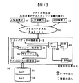
図1は、記憶制御装置配下の記憶装置がディスクアレイ装置の場合の記憶システムのハードウエア構成図である。図1において、10、20、30は、データ処理を行う中央処理装置としての上位装置である。
FIG. 1 is a hardware configuration diagram of a storage system when a storage device under the storage control device is a disk array device. In FIG. 1,
40は、本発明を実施したディスクアレイ装置の記憶制御装置である。図1に示すように、記憶制御装置40は、上位装置10、20、30との間のデータ転送を制御するためのDMA(ダイレクト アクセス メモリ)を含むプロトコルプロセッサであるファイバチャネル制御部41、記憶制御装置全体を制御するマイクロプロセッサ42、制御装置の動作を制御するマイクロプログラム及び制御用データを保存する制御メモリ43、キャッシュへのデータの読み書きを制御するキャッシュ制御部44、書き込みデータ及びディスクドライブからの読み出しデータを一時バッファリングしておくディスクキャッシュ45、ディスクドライブとの間のデータ転送を制御するためのDMAを含むプロトコルプロセッサであるデバイスインタフェース制御部46、装置構成情報を記憶制御装置へ入力するパネル47から構成されている。
Reference numeral 40 denotes a storage control device of the disk array device embodying the present invention. As shown in FIG. 1, the storage control device 40 includes a fiber channel control unit 41 which is a protocol processor including a DMA (direct access memory) for controlling data transfer between the
50は、記憶制御装置40の配下にあるディスクアレイ装置である。ディスクアレイ装置50は、上位装置のデータを格納する装置で、複数台の個別ディスクを冗長性を持つように配置構成したものである。
ディスクアレイ装置50を構成するディスクは、論理的に分割し、分割した区画をそれぞれ異なるRAIDレベルに設定することができる。この区画をRAIDグループという。このRAIDグループをさらに論理的に分割したSCSIのアクセス単位である領域をLU(Logical Unit)といい、その領域は、各々、LUN(Logical Unit Number)という番号を持つ。本実施の形態ではディスクアレイ装置50は、LUN0番のLUである、LU0(51)とLUN1番のLUである、LU1(52)の2個の領域を有する場合を示している。
The disks constituting the
なお、LUの数は、図1に示す2個に限らずもっと多くてもよく、シングルターゲット機能の場合、ターゲット当り最大8個までLUを設定できる。 The number of LUs is not limited to two as shown in FIG. 1, and may be larger. In the case of the single target function, up to eight LUs can be set per target.
また、本実施の形態では、LUなる記憶領域をアクセス単位としているが、アクセス単位とする記憶領域としては、物理ボリューム単位やRAIDグループ単位の記憶領域も可能である。 In the present embodiment, the storage area as an LU is used as an access unit, but a storage area as an access unit may be a storage area in a physical volume unit or a RAID group unit.
上位装置10、20、30と記憶制御装置40は、ファイバチャネル60をインタフェースとし、ファブリック(Fabric)という装置を介して接続されている。
The
図1のシステムの動作を、上位装置10が記憶制御装置40経由でディスクアレイ装置50とデータ転送を行う場合を例にとり、制御の流れ、データの流れを中心に説明する。
The operation of the system shown in FIG. 1 will be described focusing on a control flow and a data flow, taking as an example a case where the host device 10 performs data transfer with the
上位装置10がアクセス要求を出すと、その要求を認識したファイバチャネル制御部41はマイクロプロセッサ42に割り込み要求を発行する。マイクロプロセッサ42は、上位装置からのコマンド情報及び本発明で必要な制御情報を、制御メモリ43に格納する。
When the host device 10 issues an access request, the fiber channel control unit 41 that recognizes the request issues an interrupt request to the
コマンド情報が、ライトコマンドの場合は、マイクロプロセッサ42はファイバチャネル制御部41にデータ転送を指示し、転送されたデータをキャッシュ制御部44を経由してキャッシュ45に格納する。上位装置10に対しては、ファイバチャネル制御部41がライト完了報告を行う。ライト完了報告後、マイクロプロセッサ42がデバイスインタフェース制御部46を制御し、ディスクアレイ装置50に対し、データ及び冗長データを書き込む。この場合、一般のRAID5の動作においては、旧データ、旧パリティ及び新データに基いて新パリティを作成するが、本発明の制御によれば、マイクロプロセッサ42が、デバイスインタフェース制御部46及びキャッシュ制御部44、制御メモリ43、キャッシュ45を用いて行なう。
If the command information is a write command, the
一方、上位装置10からコマンド情報として、リードコマンド情報を受けた場合は、マイクロプロセッサ42は、デバイスインタフェース制御部46に指示を出し、当該アクセス要求のデータブロックが格納されたディスクアレイ装置50へアクセスしてデータを読み出し、キャッシュ制御部44を経由してキャッシュ45へデータを格納する。マイクロプロセッサ42は、ファイバチャネル制御部41に指示を出し、ファイバチャネル制御部41は、キャッシュ45に格納したデータを上位装置10に転送し、転送後上位装置へリード完了報告を行なう。
On the other hand, when receiving read command information as command information from the host device 10, the
次にファイバチャネル60の特長を説明する。ファイバチャネルは最大10kmの距離で100MB/sの転送が可能な高速インタフェースである。ファイバチャネルのアーキテクチャは転送元のバッファから転送先のバッファへデータを送るが、データのフォーマットや内容には無関係に一台の装置から別の装置へバッファの内容を移すため、異なるネットワーク通信プロトコルを処理するオーバヘッドがなく、高速データ転送を実現している。上位論理層にはTCP/IP、SCSI、ESCON、IPI等の種々のレイヤを搭載可能である。すなわち、他のインタフェースと論理的に互換性を持つ。複雑な装置間の接続/交換という機能はFabricと呼ぶ装置が行ない、論理パス多重構成を組むことが可能である。
Next, the features of the
ファイバチャネルがデータをやりとりする基本単位をフレームと言う。次に、このフレームについて、図2を用いて説明する。 A basic unit in which data is exchanged by the Fiber Channel is called a frame. Next, this frame will be described with reference to FIG.
図2に示すように、フレーム70は、スタートオブフレームSOF(Start Of Frame)71、フレームヘッダ72、データフィールド73、サイクリックリダンダンシチェックCRC(Cyclic Redundancy
Check)74及びエンドオブフレームEOF(End Of Frame
)75で構成される。
As shown in FIG. 2, the frame 70 is composed of a start of frame SOF (Start Of Frame) 71, a
Check) 74 and End of Frame EOF (End Of Frame)
) 75.
SOF71は、フレームの先頭に置く4バイトの識別子である。
The
EOF75は、フレームの最後につける4バイトの識別子で、SOF71とEOF75によりフレームの境界を示す。ファイバチャネルではフレームがない時はアイドル(idle)という信号が流れている。
The
フレームヘッダ72は、フレームタイプ、上位プロトコルタイプ、送信元と送信先のN_Port_ID情報、N_Port_Name情報等を含む。N_Port_IDはアドレスを表わし、N_Port_Nameはポートの識別子を表わす情報である。
The
データフィールド73の先頭部には上位レイヤのヘッダを置くことができる。
At the head of the
これにデータそのものを運ぶペイロード部が続く。CRC74は、フレームヘッダとデータフィールドのデータをチェックするための、4バイトのチェックコードである。 This is followed by the payload that carries the data itself. The CRC 74 is a 4-byte check code for checking the data of the frame header and the data field.
上記フレームヘッダ72のフォーマット80を、図3に示す。フレームヘッダフォーマット80において、デスティネーションアイデンティファイアD_ID(Destination ID)81はフレーム受け取り側のアドレス識別子であり、また、ソースアイデンティファイアS_ID(Source ID)82はフレーム送信側のN_Portアドレス識別子であり、各々、N_Port_ID情報等を含む。
The format 80 of the
次に図4を用いて、フレームを構成するデータフィールド73のペイロードの1つである、ファイバチャネルプロトコルコマンドFCP_CMND(Fibre Channel Protocol for SCSI Command)のペイロード90の説明を行なう。
Next, the payload 90 of the Fiber Channel Protocol command FCP_CMND (Fibre Channel Protocol for SCSI Command), which is one of the payloads of the
FCPロジカルユニットナンバFCP_LUN(FCP Logical Unit Number)フィールド91には、コマンドを発行するロジカルユニット番号LUNが指定される。 FCPコントロールFCP_CNTL(FCP Control)フィールド92には、コマンド制御パラメータが指定される。
そして、 FCP コマンドデスクリプタブロックFCP_CDB(FCP Command Discriptor Block)フィールド93には、SCSIコマンドディスクリプタブロック(SCSI Command Descriptor Block)が格納され、リードコマンドRead等のコマンド種類、LUN等のアドレス、ブロック数が示される。FCPデータレングスFCP_DL(FCP Data Length)フィールド94には、当該コマンドにより転送されるデータ量がバイト数で指定される。
In the FCP logical unit number FCP_LUN (FCP Logical Unit Number)
The FCP command descriptor block FCP_CDB (FCP Command Descriptor Block)
以上のように構成されたフレームによってデータのやりとりが行われる。 Data is exchanged by the frame configured as described above.
フレームは機能に基づいてデータフレームとリンク制御フレームとに大別される。データフレームは、情報を転送するために用い、データフィールドのペイロード部に上位プロトコルで使用するデータ、コマンドを搭載する。 Frames are broadly classified into data frames and link control frames based on functions. The data frame is used to transfer information, and carries data and commands used in the upper layer protocol in the payload portion of the data field.
一方、リンク制御フレームは、一般に、フレーム配信の成功あるいは不成功を示すのに使われる。フレームを1個受領したことを示したり、ログインする場合に転送に関するパラメータを通知したりするフレーム等がある。 On the other hand, link control frames are generally used to indicate success or failure of frame distribution. There are frames that indicate that one frame has been received, and that notify parameters related to transfer when logging in.
次に、図5を用いて、「シーケンス」について説明する。ファイバチャネルに
おけるシーケンスは、あるN_Portから別のN_Portへ、一方向に転送される関連するデータフレームの集まりのことを言い、SCSIのフェーズに相当する。シーケンスの集まりをエクスチェンジと呼ぶ。例えばコマンドを発行して、そのコマンドの終了までに、そのコマンド実行のためにやりとりされるシーケンスの集まり(コマンド発行、データ転送、終了報告)がエクスチェンジとなる。このように、エクスチェンジはSCSIのI/Oに相当する。
Next, the “sequence” will be described with reference to FIG. A sequence in Fiber Channel refers to a collection of related data frames that are transferred in one direction from one N_Port to another, and corresponds to a phase of SCSI. A collection of sequences is called an exchange. For example, a set of sequences (command issuance, data transfer, end report) exchanged to execute the command by issuing the command and ending the command is exchanged. Thus, an exchange is equivalent to SCSI I / O.
図5(a)、(b)及び(c)は、それぞれ、ログインシーケンス(100)、
リードコマンドシーケンス(110)及びライトコマンドシーケンス(120)を示す。
FIGS. 5A, 5B and 5C respectively show a login sequence (100),
A read command sequence (110) and a write command sequence (120) are shown.
ファイバチャネルインタフェースでは、上位装置がデバイスに対し、通信パラメータを含むポートログインPLOGI(N_Port Login)フレームを送り、デバイスがこれを受け付けることで通信が可能となる。これをログインと呼ぶ。図5(a)に、ログインシーケンス(100)を示す。 In the fiber channel interface, the host apparatus sends a port login PLOGI (N_Port Login) frame including communication parameters to the device, and the device accepts the frame to enable communication. This is called login. FIG. 5A shows a login sequence (100).
図5(a)のログインシーケンス(100)において、まず、シーケンス101で、上位装置はデバイスに対し、PLOGIフレームを送り、ログインの要求を行なう。デバイスはアクノレッジACK(Acknowledge)フレームを上位装置に送り、PLOGIフレームを受け取ったことを知らせる。
In the login sequence (100) of FIG. 5A, first, in
次いで、シーケンス102において、デバイスは、ログイン要求を受け付ける場合はアクセプトACC(Accept)フレームを、要求を拒絶する場合はリンクサービスリジェクトLS−RJT(Link Service Reject)フレームを、それぞれ、上位装置に送る。
Next, in
次に、図5(b)のリードコマンドのシーケンス(110)を説明する。 Next, the sequence (110) of the read command in FIG. 5B will be described.
シーケンス111において、上位装置はデバイスに対し、FCP_CMNDフレームを送り、リード要求を行なう。デバイスはACKフレームを上位装置に送る。
In
シーケンス102では、デバイスは、FCPトランスファレディFCP_XFER_RDY(FCP Transfer Ready)フレームを上位装置に送り、データ転送の準備ができたことを知らせる。上位装置はACKフレームをデバイスに送る。
In the
シーケンス113に進み、デバイスはFCPデータ(FCP_DATA)フレームを上位装置に送り、データを転送する。上位装置はACKフレームをデバイスに送る。 Proceeding to sequence 113, the device sends an FCP data (FCP_DATA) frame to the higher-level device and transfers the data. The higher-level device sends an ACK frame to the device.
次のシーケンス114では、デバイスはFCP_RSPフレームを上位装置に送り、データの転送が正常終了したことを知らせる。上位装置はACKフレームをデバイスに送る。
In the
次に、図5(c)のライトコマンドのシーケンス(120)を説明する。 Next, the write command sequence (120) in FIG. 5C will be described.
シーケンス121において、上位装置はデバイスに対し、FCP_CMNDフレームを送り、ライト要求を行なう。デバイスはACKフレームを上位装置に送る。
In a
次いで、シーケンス122において、デバイスはFCP_XFER_RDYフレームを上位装置に送り、データ書き込みが可能であることを知らせる。上位装置はACKフレームをデバイスに送る。
Next, in a
さらに、シーケンス123において、上位装置はFCP_DATAフレームをデバイスに送り、データを転送する。デバイスはACKフレームを上位装置に送る。
Further, in the
最後に、シーケンス123において、デバイスは、FCPレスポンスFCP_RSP(FCP Response)フレームを上位装置に送り、データの受け取りが正常終了したことを知らせる。上位装置はACKフレームをデバイスに送る。
Finally, in
以上、図1ないし図5によって、一般的なシステム構成、フォーマット及びシーケンスを説明したが、以下、本発明によるセキュリティチェックについて説明する。 The general system configuration, format, and sequence have been described with reference to FIGS. 1 to 5, and the security check according to the present invention will be described below.
初めに、PLOGI時におけるN_Port_Name情報を用いたセキュリティチェックについて、説明を行なう。 First, a security check using N_Port_Name information at the time of PLOGI will be described.
本発明では、図1において、まず、上位装置10、20、30の立ち上がる以前に、ユーザは記憶制御装置40のマイクロプロセッサ42にアクセス可能な上位装置のリストを設定する。すなわち、上位装置を識別できるN_Port_Name、N_Port_ID等の情報を、パネル47を用いて入力する。この際、パネルへの入力上の機密保護機能を実現するために、入力に際してパスワードを要求し、セキュリティを強化できる。
In the present invention, first, in FIG. 1, before the
パスワードを入力し、既に設定したパスワードとの一致が図られた場合、記憶制御装置のポート毎にアクセス可能な上位装置のN_Port_Name情報を入力し、入力情報を制御テーブルに格納する。 When the password is entered and the password matches the already set password, N_Port_Name information of the host device accessible for each port of the storage control device is entered, and the input information is stored in the control table.
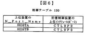
いま、例として、上位装置10、20はディスクアレイ装置50にアクセス可能、上位装置30はディスクアレイ装置50にはアクセス不可能とし、N_Port_Nameを、上位装置10はHOSTA、上位装置20はHOSTB、上位装置30はHOSTCとし、記憶制御装置40のファイバチャネル制御部41のポートをCTL0P0とした場合、ログイン要求制御テーブル130は、図6のようになる。
Now, as an example, the higher-
図6に示すこのログイン要求制御テーブル130を、不揮発メモリ上に設定することにより、万一の電源瞬断時にも管理情報を守ることができる。 By setting the login request control table 130 shown in FIG. 6 in the nonvolatile memory, the management information can be protected even in the event of a momentary power failure.
また、ログイン要求制御テーブル130に格納した情報は、電源を切断した場合はハードディスク領域50へ格納する。または情報の更新時にメモリ43とディスク50へ反映を行なう。これにより記憶制御装置40は、当該情報を再設定されるまで恒久的に保持することができる。
The information stored in the login request control table 130 is stored in the
なお、ファイバチャネルにおいてノードやポートの識別に使用される自ノード情報として、N_Port_Nameの他に、N_Port_IDがあるが、N_Port_IDは変更される可能性があり、ユーザが管理する数値ではないため、N_Port_Name情報をセキュリティのためのチェック対象とするのが望ましい。 In addition, there is N_Port_ID in addition to N_Port_Name as own node information used for identification of a node or a port in the Fiber Channel. However, since N_Port_ID may be changed and is not a numerical value managed by a user, the N_Port_Name information Should be checked for security.
次に、図1及び図7を用いて上位装置のログイン要求に対する記憶制御装置のフレーム処理手順の説明を行なう。 Next, a frame processing procedure of the storage control device in response to a login request from the host device will be described with reference to FIGS.
(ステップS71)
上位装置10、20、30が立ち上がり、各々、N_Port_Name情報を格納したログイン要求フレームであるPLOGIフレームを発行する。記憶制御装置40のマイクロプロセッサ42は、当該フレームを受領すると、まずこのフレームを受領したことを示すACKフレームを各上位装置に返す。
(Step S71)
The
(ステップS72)
そしてマイクロプロセッサ42は、当該フレームに格納されているN_Port_Name情報を切り出し、そのN_Port_Name情報が、既に設定され、保持されている制御テーブル内のN_Port_Nameリストに登録されているかどうか、比較を行なう。
(Step S72)
Then, the
(ステップS73)(ステップS74)(ステップS75)
上位装置10、20の発行した当該フレームに格納されているN_Port_Name情報は、制御テーブル内に登録されているN_Port_Name情報と一致するため、記憶制御装置40のマイクロプロセッサ42は、上位装置10、20に対してはログイン要求を受け付けた印として、ACCフレームを返し、ログイン処理を続行する。
(Step S73) (Step S74) (Step S75)
Since the N_Port_Name information stored in the frame issued by the higher-
(ステップS73)(ステップS76)
一方、上位装置30の発行した当該フレームに格納されているN_Port_Name情報は、制御テーブル内に登録されているN_Port_Name情報と一致しないため、記憶制御装置40のマイクロプロセッサ42は、上位装置30に対しては接続を拒絶するリジェクトパラメータをいれたLS_RJTフレームを返す。
(Step S73) (Step S76)
On the other hand, since the N_Port_Name information stored in the frame issued by the higher-
以上のように、記憶制御装置40が、ログイン要求制御テーブル130を用いて、上位装置と記憶制御装置のポートの対応付けを管理することにより、ユーザはポート毎に上位装置からの不正アクセスを抑止することができ、セキュリティが保持できる。 As described above, the storage control device 40 manages the correspondence between the host device and the port of the storage control device using the login request control table 130, so that the user can prevent unauthorized access from the host device for each port. Security can be maintained.
次に、本発明において、ディスクアレイ装置の記憶領域であるLUN毎に、N_Port_Name情報を用いてセキュリティチェックを実施する方法について説明する。 Next, in the present invention, a method of performing a security check using N_Port_Name information for each LUN that is a storage area of the disk array device will be described.
本発明では、まず上位装置10、20、30の立ち上がる以前に、記憶制御装置40のマイクロプロセッサ42に、LUN毎にアクセス可能な上位装置のリストを設定する。上位装置を識別できるN_Port_Name、N_Port_ID等の情報を、パネル47を用いて入力する。この際、パネル47への入力上の機密保護機能を実現するために、入力に際してパスワードを要求し、セキュリティを強化することができる。
In the present invention, first, before the
パスワードを入力し、既に設定したパスワードとの一致が図られた場合、LUN毎に記憶制御装置のポート及びアクセス可能な上位装置のN_Port_Name情報を入力し、入力情報を制御テーブルに格納する。 When the password is entered and the password matches the already set password, the port of the storage control device and the N_Port_Name information of the accessible higher-level device are input for each LUN, and the input information is stored in the control table.
LU0(51)は、上位装置10から記憶制御装置40のファイバチャネル制御部41のポート経由でアクセス可能、LU1(52)は、上位装置20から記憶制御装置40のファイバチャネル制御部41のポート経由でアクセス可能とし、
N_Port_Nameを、上位装置10はHOSTA、上位装置20はHOSTB、記憶制御装置40のファイバチャネル制御部41のポートをCTL0P0、とした場合、I/O要求制御テーブル140は、図8のようになる。
LU0 (51) can be accessed from the host device 10 via the port of the fiber channel control unit 41 of the storage control device 40, and LU1 (52) can be accessed from the
When N_Port_Name is HOSTA for the host device 10, HOSTB for the
図8に示すこのI/O要求制御テーブル140は不揮発メモリ上に設定すると、
万一の電源瞬断時にも管理情報を守ることができる。
When this I / O request control table 140 shown in FIG. 8 is set in the nonvolatile memory,
Management information can be protected even in the event of a power interruption.
また、図8のI/O要求制御テーブル140に格納した情報は、電源を切断した場合は、ハードディスク領域50へ格納する。または情報の更新時にメモリ43とディスク50へ反映を行なう。これにより記憶制御装置40は当該情報を再設定されるまで恒久的に保持することができる。
The information stored in the I / O request control table 140 of FIG. 8 is stored in the
本実施例ではチャネルパスルートは1通りであるが、複数のチャネルパスルートを有するシステムにおいても同様である。 In this embodiment, there is one channel path route, but the same applies to a system having a plurality of channel path routes.
以下に図1及び図9を用いて、上位装置のI/O要求に対する記憶制御装置のフレーム処理手順の説明を行なう。上記の例ではPLOGI時にセキュリティチェックを行なったが、本実施の形態では、各SCSIコマンド毎にチェックを行なう。 The frame processing procedure of the storage control device in response to an I / O request of a higher-level device will be described below with reference to FIGS. In the above example, the security check was performed at the time of PLOGI, but in the present embodiment, the check is performed for each SCSI command.
(ステップS91)
上位装置10がLU0(51)にI/O要求を出したい場合、上位装置10は記憶制御装置40に対し、SCSI CDBを格納したフレームを発行する。記憶制御装置40がこのフレームを受領した場合、まず、このフレームを受領したことを示すACKフレームを上位装置10に返す。
(Step S91)
When the host device 10 wants to issue an I / O request to the LU 0 (51), the host device 10 issues a frame storing the SCSI CDB to the storage control device 40. When the storage control device 40 receives this frame, it first returns an ACK frame indicating that this frame has been received to the host device 10.
(ステップS92)
そしてマイクロプロセッサ42は、当該フレームに格納されているN_Port_Name情報及びCDB内のLUN番号を切り出し、そのN_Port_Name情報及びLUN番号が、当該マイクロプロセッサ42に既に設定され保持されている制御テーブル内のリストに登録されているかどうか、比較を行なう。
(Step S92)
Then, the
(ステップS93)(ステップS94)(ステップS95)
管理テーブル内には、「上位装置10は、LU0(51)をアクセス可能であ
る」と登録されているため、記憶制御装置40のマイクロプロセッサ42はコマンドを受領し、I/O処理を継続する。
(Step S93) (Step S94) (Step S95)
In the management table, "upper device 10 can access LU0 (51)" is registered, so
(ステップS91)
一方、上位装置20が記憶制御装置40にLU0(51)のI/O要求フレームを発行し、記憶制御装置40がこのSCSI CDBを格納したフレームを受領した場合、マイクロプロセッサ42は、まずこのフレームを受領したことを示すACKフレームを上位装置20に返す。
(Step S91)
On the other hand, when the
(ステップS92)
そしてマイクロプロセッサ42は、当該フレームに格納されているN_Port_Name情報及びCDB内のLUN番号を切り出し、そのN_Port_Name情報及びLUN番号が、管理テーブル内にあるかどうかの検索を行なう。
(Step S92)
Then, the
(ステップS93)(ステップS96)
検索を行なった結果、管理テーブル内に、該当するLUNおよびN_Port_Nameの組合わせが存在しないため、記憶制御装置40のマイクロプロセッサ42は、上位装置20にLS_RJTフレームを送って、I/O要求を拒絶する。
(Step S93) (Step S96)
As a result of the search, since the combination of the corresponding LUN and N_Port_Name does not exist in the management table, the
こうして記憶制御装置は不正なアクセスを防止することができる。 Thus, the storage control device can prevent unauthorized access.
ここではログイン及びI/O要求フレームを取り上げたが、これら以外の他の上位装置フレームに格納されているN_Port_Name情報を比較してもよい。 Although the login and I / O request frames have been described here, N_Port_Name information stored in other higher-level device frames may be compared.
なお、ファイバチャネル接続記憶制御装置配下の記憶装置がディスクアレイ装置に限らず、光ディスク装置、光磁気ディスク装置及び磁気テープ装置並びにこれらのライブラリ装置である場合にも本発明を適用できる。 The present invention can be applied to a case where the storage devices under the fiber channel connection storage control device are not limited to a disk array device but are an optical disk device, a magneto-optical disk device, a magnetic tape device, and a library device thereof.
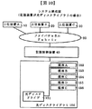
記憶制御装置配下の記憶装置が光ディスクライブラリ装置の場合に本発明を適用した場合の概要を図10を用いて説明する。150は記憶制御装置40配下の光ディスクライブラリ装置であり、151は光ディスクドライブ、152から156は光ディスクの媒体である。 An overview when the present invention is applied to a case where the storage device under the storage control device is an optical disk library device will be described with reference to FIG. Reference numeral 150 denotes an optical disk library device under the control of the storage controller 40; 151, an optical disk drive; and 152 to 156, optical disk media.
ユーザは上位装置10、20、30が立ち上る前にパネルを使用して、媒体、ドライブ、ポートとN_Port_Name情報との対応付けを設定し、上位装置のアクセス権限をマイクロプログラムに保持しておく。
Before the
媒体152、153、154は、上位装置10からアクセス可能、媒体D155、E156は上位装置20からアクセス可能とし、N_Port_Nameを上位装置10はHOSTA、上位装置20はHOSTB、記憶制御装置40のポートをCTL0P0、光ディスクドライブA151をDRIVE0、媒体A152、B153、C154、D155、E156を各々MEDA、MEDB、MEDC、MEDD、MEDE、とした場合、要求制御テーブル160は、図11のようになる。
The
各上位装置がI/O要求フレームを発行した際、フレームを構成するペイロード内のCDBにボリューム情報が格納されているため、記憶制御装置40は当該フレームを受領した際、フレーム内のN_Port_Name情報及びペイロード内の媒体識別子を,当該記憶制御装置40に既に設定され、保持されている制御テーブルと比較を行なえばよい。このように、本発明を応用することによって、
記憶制御装置は上位装置からの不正アクセスを防止可能である。
When each higher-level device issues an I / O request frame, the volume information is stored in the CDB in the payload constituting the frame. Therefore, when the storage controller 40 receives the frame, the storage controller 40 checks the N_Port_Name information and the The medium identifier in the payload may be compared with the control table already set and held in the storage control device 40. Thus, by applying the present invention,
The storage control device can prevent unauthorized access from a host device.
10、20,30…上位装置、40…記憶制御装置、41…ファイバチャネル制御部、42…マイクロプロセッサ、43…制御メモリ、44…キャッシュ制御部、45…キャッシュ、46…デバイスインタフェース制御部、47…パネル、50…ディスクアレイ装置、51…ロジカルユニット0、52…ロジカルユニット1、60…ファイバチャネル、70…フレーム、71…スタートオブフレームSOF(Start Of Frame)、72…フレームヘッダ、73…データフィールド、74…サイクリックリダンダンシチェックCRC(Cyclic
Redundancy Check)、75…エンドオブフレームEOF(End Of Frame)、80…フレームヘッダのフォーマット、81…デスティネーションアイデンティファイアD_ID(Destination ID
)、82…ソースアイデンティファイアS_ID(Source ID)、90…ファイバチャネルプロトコルコマンドFCP_CMNDペイロード(Fibre Channel Protocol for SCSI Command)、91…ファイバチャネルプロトコルロジカルユニットナンバFCP_LUN(FCP Logical Unit Number)、92…ファイバチャネルプロトコルコントロールFCP_CNTL(FCP Control)、93…ファイバチャネルプロトコルコマンドデスクリプタブロックFCP_CDB(FCP Command Descriptor Block)、94…ファイバチャネルプロトコルデータレングスFCP_DL( FCP Data Length)、100…ログイン、110…リードコマンド、120…ライトコマンド、130…ログイン要求制御テープル、140…磁気ディスクアレイI/O要求制御テープル、150…光ディスクライブラリ、160…光ディスクライブラリI/O要求制御テーブル
10, 20, 30: Host device, 40: Storage controller, 41: Fiber channel controller, 42: Microprocessor, 43: Control memory, 44: Cache controller, 45: Cache, 46: Device interface controller, 47 ... Panel, 50 ... Disk array device, 51 ...
Redundancy Check), 75: End of Frame (EOF), 80: Format of frame header, 81: Destination Identifier D_ID (Destination ID)
), 82: Source Identifier S_ID (Source ID), 90: Fiber Channel Protocol Command FCP_CMND Payload (Fibre Channel Protocol for SCSI Command), 91: Fiber Channel Protocol Logical Unit Number FCP_LUN (FCP Logical Unit, 92 Fiber) Channel Protocol Control FCP_CNTL (FCP Control), 93: Fiber Channel Protocol Command Descriptor Block FCP_CDB (FCP Command Descriptor Block), 94: Fiber Channel Protocol Data Length FCP_DL (FCP Data Length), 100: Login, 110: Lee Command, 120 write command, 130 login request control table, 140 magnetic disk array I / O request control table, 150 optical disk library, 160 optical disk library I / O request control table
Claims (2)
前記記憶システムは、
記憶領域を有し前記上位装置から送信されるデータを記憶する記憶装置と、前記上位装置から前記記憶装置へのアクセスを制御する記憶制御装置を有し、さらに前記記憶制御装置は前記上位装置を識別するN_Port_Nameと、前記記憶領域を識別するLUN(Logical Unit Number)と、を有するテーブルを備え、
PLOGI時に、前記上位装置から前記記憶システムに送信されたPLOGIフレームに格納された上位装置の識別情報と前記テーブルに記載されている上位装置の識別情報が一致するか比較し、一致する場合は前記上位装置にログイン可能であることを通知する第一の工程と、
前記PLOGIの承認後の前記上位装置からのI/O要求時に、前記上位装置から前記記憶システムに送信されたI/O要求フレームに格納された上位装置の識別情報及びアクセス要求先の記憶領域の識別情報と前記テーブルに記載されている上位装置の識別情報及びアクセス要求先の記憶領域の識別情報が一致するか比較し、一致する場合は前記上位装置にI/O可能であることを通知する第二の工程とを有し、前記上位装置から前記記憶領域へのアクセスを制御することを特徴とするアクセス制御方法。 An access control method in a storage system connected to a plurality of higher-level devices via a fiber channel,
The storage system comprises:
A storage device that has a storage area and stores data transmitted from the higher-level device, and a storage controller that controls access to the storage device from the higher-level device, and the storage controller further controls the higher-level device. A table having N_Port_Name for identifying, and LUN (Logical Unit Number) for identifying the storage area,
At the time of PLOGI, the identification information of the higher-level device stored in the PLOGI frame transmitted from the higher-level device to the storage system is compared with the identification information of the higher-level device described in the table. A first step of notifying that the host device can be logged in;
Upon an I / O request from the higher-level device after the approval of the PLOGI, the identification information of the higher-level device stored in the I / O request frame transmitted from the higher-level device to the storage system and the storage area of the access request destination The identification information, the identification information of the higher-level device described in the table, and the identification information of the storage area of the access request destination are compared with each other, and if they match, the upper-level device is notified that I / O is possible. An access control method, comprising: controlling access to the storage area from the host device.
前記記憶システムは、
記憶領域を有し前記上位装置から送信されるデータを記憶する記憶装置と、前記上位装置から前記記憶装置へのアクセスを制御する記憶制御装置を有し、さらに前記記憶制御装置は前記上位装置を識別するN_Port_IDと、前記記憶領域を識別するLUN(Logical Unit Number)と、を有するテーブルを備え、
PLOGI時に、前記上位装置から前記記憶システムに送信されたPLOGIフレームに格納された上位装置の識別情報と前記テーブルに記載されている上位装置の識別情報が一致するか比較し、一致する場合は前記上位装置にログイン可能であることを通知する第一の工程と、
前記PLOGIの承認後の前記上位装置からのI/O要求時に、前記上位装置から前記記憶システムに送信されたI/O要求フレームに格納された上位装置の識別情報及びアクセス要求先の記憶領域の識別情報と前記テーブルに記載されている上位装置の識別情報及びアクセス要求先の記憶領域の識別情報が一致するか比較し、一致する場合は前記上位装置にI/O可能であることを通知する第二の工程とを有し、前記上位装置から前記記憶領域へのアクセスを制御することを特徴とするアクセス制御方法。
An access control method in a storage system connected to a plurality of higher-level devices via a fiber channel,
The storage system comprises:
A storage device that has a storage area and stores data transmitted from the higher-level device, and a storage controller that controls access to the storage device from the higher-level device, and the storage controller further controls the higher-level device. A table having N_Port_ID for identifying, and LUN (Logical Unit Number) for identifying the storage area,
At the time of PLOGI, the identification information of the higher-level device stored in the PLOGI frame transmitted from the higher-level device to the storage system is compared with the identification information of the higher-level device described in the table. A first step of notifying that the host device can be logged in;
Upon an I / O request from the higher-level device after the approval of the PLOGI, the identification information of the higher-level device stored in the I / O request frame transmitted from the higher-level device to the storage system and the storage area of the access request destination The identification information, the identification information of the higher-level device described in the table, and the identification information of the storage area of the access request destination are compared with each other, and if they match, the upper-level device is notified that I / O is possible. An access control method, comprising: controlling access to the storage area from the host device.
Priority Applications (1)
| Application Number | Priority Date | Filing Date | Title |
|---|---|---|---|
| JP2004212455A JP2004362600A (en) | 2004-07-21 | 2004-07-21 | Memory control device and memory system |
Applications Claiming Priority (1)
| Application Number | Priority Date | Filing Date | Title |
|---|---|---|---|
| JP2004212455A JP2004362600A (en) | 2004-07-21 | 2004-07-21 | Memory control device and memory system |
Related Parent Applications (1)
| Application Number | Title | Priority Date | Filing Date |
|---|---|---|---|
| JP2000118493A Division JP3633436B2 (en) | 1997-05-29 | 2000-04-14 | Computer system |
Publications (2)
| Publication Number | Publication Date |
|---|---|
| JP2004362600A true JP2004362600A (en) | 2004-12-24 |
| JP2004362600A5 JP2004362600A5 (en) | 2005-06-16 |
Family
ID=34056389
Family Applications (1)
| Application Number | Title | Priority Date | Filing Date |
|---|---|---|---|
| JP2004212455A Pending JP2004362600A (en) | 2004-07-21 | 2004-07-21 | Memory control device and memory system |
Country Status (1)
| Country | Link |
|---|---|
| JP (1) | JP2004362600A (en) |
Cited By (2)
| Publication number | Priority date | Publication date | Assignee | Title |
|---|---|---|---|---|
| JP2007140962A (en) * | 2005-11-18 | 2007-06-07 | Hitachi Ltd | Disk array system and security method |
| EP2477376A1 (en) | 2011-01-12 | 2012-07-18 | Fujitsu Limited | Communication control apparatus, communication system, information processing apparatus, and communication control method |
-
2004
- 2004-07-21 JP JP2004212455A patent/JP2004362600A/en active Pending
Cited By (4)
| Publication number | Priority date | Publication date | Assignee | Title |
|---|---|---|---|---|
| JP2007140962A (en) * | 2005-11-18 | 2007-06-07 | Hitachi Ltd | Disk array system and security method |
| EP2477376A1 (en) | 2011-01-12 | 2012-07-18 | Fujitsu Limited | Communication control apparatus, communication system, information processing apparatus, and communication control method |
| JP2012147218A (en) * | 2011-01-12 | 2012-08-02 | Fujitsu Ltd | Communication controller, communication system, information processor and communication control method |
| US8984088B2 (en) | 2011-01-12 | 2015-03-17 | Fujitsu Limited | Communication control apparatus, communication system, information processing apparatus, and communication control method |
Similar Documents
| Publication | Publication Date | Title |
|---|---|---|
| JP3987672B2 (en) | Storage control device and storage system | |
| US8422677B2 (en) | Storage virtualization apparatus comprising encryption functions | |
| US7107421B2 (en) | Data migration method and a data migration apparatus | |
| US7363455B2 (en) | Apparatus and method for partitioning and managing subsystem logics | |
| US20020095549A1 (en) | Disk storage system | |
| JP4990442B2 (en) | Storage control device and computer system | |
| US20090327758A1 (en) | Storage apparatus and data processing method for storage apparatus | |
| US20090177895A1 (en) | Controller for controlling logical volume-related settings | |
| JP4497957B2 (en) | Storage control system | |
| JP2004362600A (en) | Memory control device and memory system | |
| JP2007250009A (en) | Storage control device and storage system | |
| US20060101169A1 (en) | Device and method for generating a logical path between connection of control device connected to a host device and memory device provided in said control device |
Legal Events
| Date | Code | Title | Description |
|---|---|---|---|
| A521 | Request for written amendment filed |
Free format text: JAPANESE INTERMEDIATE CODE: A523 Effective date: 20041117 |
|
| A521 | Request for written amendment filed |
Free format text: JAPANESE INTERMEDIATE CODE: A523 Effective date: 20051128 |
|
| RD02 | Notification of acceptance of power of attorney |
Free format text: JAPANESE INTERMEDIATE CODE: A7422 Effective date: 20051128 |
|
| RD04 | Notification of resignation of power of attorney |
Free format text: JAPANESE INTERMEDIATE CODE: A7424 Effective date: 20060523 |
|
| A977 | Report on retrieval |
Free format text: JAPANESE INTERMEDIATE CODE: A971007 Effective date: 20060928 |
|
| A131 | Notification of reasons for refusal |
Free format text: JAPANESE INTERMEDIATE CODE: A131 Effective date: 20061019 |
|
| A521 | Request for written amendment filed |
Free format text: JAPANESE INTERMEDIATE CODE: A523 Effective date: 20061218 |
|
| A131 | Notification of reasons for refusal |
Free format text: JAPANESE INTERMEDIATE CODE: A131 Effective date: 20070807 |
|
| A521 | Request for written amendment filed |
Free format text: JAPANESE INTERMEDIATE CODE: A523 Effective date: 20071005 |
|
| A02 | Decision of refusal |
Free format text: JAPANESE INTERMEDIATE CODE: A02 Effective date: 20080623 |