JP2004356594A - Detector of spatial information using intensity modulating light - Google Patents
Detector of spatial information using intensity modulating light Download PDFInfo
- Publication number
- JP2004356594A JP2004356594A JP2003155712A JP2003155712A JP2004356594A JP 2004356594 A JP2004356594 A JP 2004356594A JP 2003155712 A JP2003155712 A JP 2003155712A JP 2003155712 A JP2003155712 A JP 2003155712A JP 2004356594 A JP2004356594 A JP 2004356594A
- Authority
- JP
- Japan
- Prior art keywords
- charge
- unit
- charges
- electrode
- photosensitive
- Prior art date
- Legal status (The legal status is an assumption and is not a legal conclusion. Google has not performed a legal analysis and makes no representation as to the accuracy of the status listed.)
- Granted
Links
Images


Abstract
Description
【0001】
【発明の属する技術分野】
本発明は、強度変調された光が照射されている空間からの光を受光することにより空間に関する各種情報を検出する強度変調光を用いた空間情報の検出装置に関するものである。
【0002】
【従来の技術】
従来から、強度変調した光を発光源から空間に照射するとともに、この空間に存在する物体により反射された反射光を感光部で受光し、発光源から照射した光と感光部で受光した光との関係に基づいて空間に関する各種情報を検出する技術が知られている。空間に関する情報とは、空間に存在する物体までの距離や空間に存在する物体の反射による受光量の変化などを意味する。
【0003】
強度変調した光を用いて物体までの距離を求めるには、変調周波数の逆数である変調周期に同期した特定の異なる位相で受光強度を複数回検出し、受光強度を検出した位相と受光強度との関係によって、発光源から照射した光と感光部で受光した光との位相差を求める。たとえば、発光源から照射される光の強度を正弦波で変調し、変調時の特定の異なる位相に対する感光部での受光強度を3回以上(望ましくは4回以上)検出すれば、位相差を求めることができる。
【0004】
いま、発光源から照射する光が図29の曲線イのように強度変調され、感光部での受光強度が図29の曲線ロのように変化したとする。ここで、曲線イの位相が0度、90度、180度、270度である4点において受光強度をサンプリングしたときの各受光強度に相当する検出値をそれぞれA0,A1,A2,A3とする。ただし、各位相における検出値A0,A1,A2,A3は、各位相における瞬間の時刻の入射光に対応するのではなく、たとえば図に集積時間Twとして示す期間における入射光に対応する。ここで、検出値A0,A1,A2,A3をサンプリングする期間内では位相差ψが変化せず、かつ発光から受光までの光の減衰率(図では減衰を無視している)にも変化がないものとすれば、検出値A0,A1,A2,A3を90度毎に求めていることから、各検出値A0,A1,A2,A3と位相差ψとの関係は、次式で表すことができる。
ψ=tan−1{(A3−A1)/(A0−A2)}
上述のようにして複数個の検出値A0,A1,A2,A3から位相差ψを求めると、変調周期T〔s〕と位相差ψ〔rad〕と光の速度c〔m/s〕とを用いて、物体までの距離L〔m〕を次式のように求めることができる。
L≒cT(ψ/4π)
上述の技術思想を実現する装置としては、1画素について1個の感光部と4個のメモリセルとを設け、1画素内の各メモリセルと感光部との間にそれぞれ設けた電気スイッチを、上述した集積時間Twに相当する期間にそれぞれオンにすることによって、各メモリセルに各検出値A0,A1,A2,A3を振り分けて蓄積するものが提案されている(たとえば、特許文献1参照)。
【0005】
【特許文献1】
特表平10−508736号公報(第7−9頁、図1、図4)
【0006】
【発明が解決しようとする課題】
ところで、特許文献1に記載された装置では、感光部とメモリセルとの間に設けたスイッチのオンオフのみによって、メモリセルに検出値A0,A1,A2,A3を蓄積するものであるから、感光部において生成した電荷のうちメモリセルに転送されなかった電荷は感光部に暫時残留する。このような残留電荷は、感光部の内部で再結合によって消滅するか、あるいはスイッチが次にオンになったときにメモリセルに転送されることになる。
【0007】
ここで、測定可能な最大距離がたとえば7.5mになる装置を想定する。この場合、変調周波数は20MHzになるから、集積時間Twは変調周期である50nsよりも短くしなければならない。一方、残留電荷が再結合によって消滅するのに要する時間は通常は100μsよりも長いから、メモリセルには集積期間Twに受光によって生成された電荷だけでなく残留電荷も転送される。つまり、メモリセルに蓄積される電荷には、検出値A0,A1,A2,A3に相当する信号電荷に加えて、残留電荷による雑音成分が混入することになる。感光部で受光する光は強度変調されているから、検出値A0,A1,A2,A3に応じて雑音成分も変化することになり、上述した演算によって位相差ψを求めようとすれば雑音成分による誤差を生じる可能性がある。
【0008】
本発明は上記事由に鑑みて為されたものであり、その目的は、感光部で生成された電荷のうち信号電荷として使用されない残留電荷を廃棄することにより、信号電荷への雑音成分の混入を抑制し、空間情報を高SN比で検出することを可能とした強度変調光を用いた空間情報の検出装置を提供することにある。
【0009】
【課題を解決するための手段】
請求項1の発明は、所定の変調周波数の変調信号で強度変調された光が照射されている空間からの光を受光し受光強度に対応する量の電荷を生成する感光部と、感光部で生成した電荷のうち信号電荷を蓄積する電荷蓄積部と、廃棄電極を備え感光部で生成した電荷のうち不要電荷として廃棄する電荷の割合が廃棄電極に印加する廃棄電圧に応じて増減する電荷廃棄部と、電荷蓄積部に蓄積した信号電荷を外部に取り出す電荷取出部と、廃棄電極に印加する廃棄電圧を変調信号の周期に同期するタイミングで変化させる制御回路部と、電荷取出部により取り出した電荷を用いて前記空間に関する情報を評価する評価部とを備えることを特徴とする。
【0010】
請求項2の発明は、請求項1の発明において、前記電荷蓄積部が、感光部で生成した電荷のうち電荷蓄積部に移動する電荷の割合を印加される制御電圧に応じて増減させる制御電極を備え、前記制御回路部が、制御電極に印加する制御電圧を一定電圧に保つことを特徴とする。
【0011】
請求項3の発明は、請求項1の発明において、前記電荷蓄積部が、感光部で生成した電荷のうち電荷蓄積部に移動する電荷の割合を印加される制御電圧に応じて増減させる制御電極を備え、前記制御回路部が、感光部で生成した電荷を電荷蓄積部に移動させる期間と電荷廃棄部に移動させる期間とが交互に生じるように制御電極への制御電圧と廃棄電極への廃棄電圧とを制御することを特徴とする。
【0012】
請求項4の発明は、所定の変調周波数の変調信号で強度変調された光が照射されている空間からの光を受光し受光強度に対応する量の電荷を生成する感光部と、制御電極を備え感光部で生成した電荷のうち信号電荷として蓄積する電荷の割合が制御電極に印加する制御電圧に応じて増減する電荷蓄積部と、廃棄電極を備え感光部で生成した電荷のうち不要電荷として廃棄する電荷の割合が廃棄電極に印加する廃棄電圧に応じて増減する電荷廃棄部と、電荷蓄積部に蓄積した信号電荷を外部に取り出す電荷取出部と、廃棄電極に印加する廃棄電圧を一定電圧に保って電荷の廃棄を行う間に制御電極に印加する制御電圧を変調信号の周期に同期するタイミングで変化させることにより感光部で生成した電荷のうち電荷蓄積部に蓄積する信号電荷の割合を変化させる制御回路部と、電荷取出部により取り出した電荷を用いて前記空間に関する情報を評価する評価部とを備えることを特徴とする。
【0013】
請求項5の発明では、請求項1ないし請求項4の発明において、半導体基板の主表面に前記感光部が複数個配列されるとともにCCDからなる前記電荷蓄積部および前記電荷取出部が前記半導体基板に設けられたCCDイメージセンサを用い、前記電荷廃棄部がCCDイメージセンサに設けたオーバーフロードレインであることを特徴とする。
【0014】
請求項6の発明では、請求項1ないし請求項5の発明において、前記感光部のうち隣接する規定の複数個ずつの感光部を組にし、前記制御回路部は、組である複数個の感光部においてそれぞれ生成された電荷を前記変調信号の周期に同期する異なる位相のタイミングで各別に電荷蓄積部に蓄積させ、前記電荷取出部は組である複数個の感光部に対応して得られた異なる位相に対応する各信号電荷を一度に取り出すことを特徴とする。
【0015】
請求項7の発明では、請求項1ないし請求項6の発明において、前記電荷蓄積部において信号電荷を蓄積する領域付近に設けた前記制御電極に遮光膜を設けたことを特徴とする。
【0016】
請求項8の発明では、請求項1ないし請求項7の発明において、前記評価部は前記空間に発光源から照射された光と前記感光部で受光した光との位相差を前記変調信号の異なる位相に対応する複数の信号電荷から求めることを特徴とする。
【0017】
請求項9の発明では、請求項8の発明において、前記評価部は前記位相差を距離に換算することを特徴とする。
【0018】
【発明の実施の形態】
以下の各実施形態では、強度変調された発光源からの光と感光部において受光した光との位相差を用いて距離を計測する測距装置に本発明の技術を用いる例を説明するが、本発明の技術思想は、距離の測定に限らず、強度変調された光の元の位相と感光部で受光した光の位相差を求める装置や、物体での反射光の変化を求める装置などにも適用可能である。
【0019】
(第1実施形態)
本実施形態では、図1に示すように、空間に光を照射する発光源2を設けてあり、発光源2から照射される光は制御回路部3によって一定の変調周波数で強度変調される。発光源2には、たとえば多数個の発光ダイオードを一平面上に配列したものや半導体レーザと発散レンズとを組み合わせたものなどを用いる。制御回路部3は、たとえば20MHzの正弦波で発光源2から照射する光を強度変調する。
【0020】
一方、前記空間からの光は受光レンズ4を通してイメージセンサ1の感光部11に入射する。感光部11は受光強度に応じた量の電荷を生成するものであり、ここではフォトダイオードを想定している。ただし、感光部11を構成するフォトダイオードの構造としてはpn接合を有する構造のほか、pin構造、MIS構造など種々構成を採用することが可能である。本実施形態では、複数個(たとえば、100×100個)の感光部11を2次元平面にマトリクス状に配列したイメージセンサ1を想定しており、イメージセンサ1の受光面である2次元平面には発光源2から光を照射した3次元空間が受光レンズ4を通してマッピングされる。つまり、イメージセンサ1が受光レンズ4を通して見る視野内に存在する物体Obは感光部11にマッピングされるから、発光源2から照射された光と各感光部11で受光した光との位相差を検出すれば、各感光部11にそれぞれ対応している物体Obの各部位までの距離を求めることができる。
【0021】
イメージセンサ1には、感光部11のほかに、感光部11で生成された電荷のうち位相差を求めるための信号電荷を蓄積する電荷蓄積部12と、電荷蓄積部12に蓄積した信号電荷をイメージセンサ1の外部に取り出す電荷取出部13と、感光部11で生成された電荷のうち信号電荷として用いない不要電荷を廃棄する電荷廃棄部14とが設けられる。電荷蓄積部12は制御電極12aを備え、制御電極12aに印加する制御電圧を変化させると感光部11から電荷蓄積部12への電荷の移動が制御される。また、電荷廃棄部14は廃棄電極14aを備え、廃棄電極14aに印加する廃棄電圧を変化させると感光部11から電荷廃棄部14への電荷の移動が制御される。ここにおいて、電荷蓄積部12は感光部11ごとに一対一に対応するように設けられ、電荷廃棄部14は複数個の感光部11に共通させて一対多に対応するように設けられる。本実施形態では、イメージセンサ1のすべての感光部11に対して1個の電荷廃棄部14を設けているものとする。電荷取出部13を通してイメージセンサ1の出力として取り出される信号電荷は評価部5に入力され、評価部5は、発光源2から照射された光と各感光部11で受光した光との位相差を求め、さらに位相差に基づいて物体Obまでの距離を求めて出力する。
【0022】
従来構成において説明したように、物体Obまでの距離を求めるには、変調信号の周期に同期したタイミングで検出値A0,A1,A2,A3を求める必要があり、感光部11で生成される電荷のうち変調信号の特定位相(たとえば、0度、90度、180度、270度の4位相)に対応する一定の時間幅Tw(図29参照)に対応した電荷を信号電荷として電荷蓄積部12に蓄積することが必要である。つまり、感光部11に入射する光の強度に対して電荷蓄積部12に蓄積する信号電荷の割合を、上述した時間幅Twに相当する期間には多くし、他の期間には少なくする(理想的には0にする)ことが必要である。感光部11への入射光量に対して信号電荷を生成する割合は感度に相当するから、イメージセンサ1を用いて物体Obまでの距離を求めるには、イメージセンサ1の感度を制御することが必要であると言える。
【0023】
上述した構成のイメージセンサ1において感度を制御するためには、制御電極12aに印加する制御電圧の大きさを適宜タイミングで制御することが考えられるが、従来構成として説明したように、制御電圧の大きさを制御するだけでは、感光部11で生成された電荷のうち不要である残留電荷が雑音成分として信号電荷に混入することになる。そこで、本実施形態では、制御電極12aに印加する制御電圧は一定電圧に保つことによって、各感光部11で生成された電荷を各感光部11に対応してそれぞれ設けた電荷蓄積部12に常時取り込むようにし、一方、廃棄電極14aについては、受光部11で生成された電荷のうち信号電荷として扱う電荷が生成される期間を除く期間に、受光部11から電荷廃棄部14に電荷が移動するように廃棄電圧を印加する。要するに、廃棄電圧を変調信号の周期に同期するタイミングで変化させることによってイメージセンサ1の感度を制御し、電荷蓄積部12に信号電荷を蓄積するのである。
【0024】
いま、図2(a)のような変調信号によって発光源2から空間に照射される光の強度が変調されているものとする。電荷蓄積部12には変調信号の複数周期(数万〜数十万周期)において1種類の検出値A0,A1,A2,A3を蓄積し、各検出値A0,A1,A2,A3の蓄積毎に蓄積した信号電荷を取り出して次の検出値A0,A1,A2,A3を蓄積する。たとえば、検出値A0を変調信号の数万周期について蓄積すると、この検出値A0に相当する信号電荷を一旦外部に取り出し、その後、検出値A1を変調信号の数万周期について蓄積するというように動作する。図2は検出値A0に相当する信号電荷を蓄積している状態を示しており、図2(b)に示すように制御電極12aに印加する制御電圧は一定電圧に保っている。また、検出値A0としては、変調信号の位相が0〜90度の期間(図29に示した従来構成における時間幅Twに相当する)において感光部11で生成された電荷を採用している。つまり、廃棄電極14aには、図2(c)のように変調信号の位相が90〜360度の期間において、感光部11で生成される電荷を不要電荷とするように廃棄電圧を印加する。要するに、感光部11から電荷蓄積部12に電荷が移動している期間のうち信号電荷を蓄積する期間(0〜90度の期間)に対応する期間以外において廃棄電圧を印加し、所望の検出値A0を得るための信号電荷を蓄積する期間以外では感光部11で生成した電荷を不要電荷として電荷廃棄部14に廃棄する。このような制御によって、図2(d)のように所望の検出値A0に対応した信号電荷を取り出すことが可能になる。図2に示す処理は変調信号の数万〜数十万周期について行われ、この期間に電荷蓄積部12に得られた信号電荷は検出値A0として電荷取出部13により評価部5に取り出され、評価部5では信号電荷に基づいて空間情報(本実施形態では物体Obまでの距離)を検出する。
【0025】
なお、上述の制御では、廃棄電極14aに廃棄電圧を印加している期間において制御電極12aにも一定電圧である制御電圧を印加しているが、廃棄電圧と制御電圧との大小関係を適宜に設定することによって、不要電荷を廃棄している期間には信号電荷の蓄積がほとんど行われないようにすることができる。また、変調信号の数万〜数十万周期について電荷を蓄積しているのは、蓄積する電荷量を多くすることによって高感度化するためであり、本実施形態では変調信号をたとえば20MHzと設定することによって、30フレーム/秒で信号電荷を取り出すとしても、数十万周期以上の蓄積が可能になる。
【0026】
上述したように、本実施形態では廃棄電極14aを備えた電荷廃棄部14を設け、感光部11に生じた電荷のうち信号電荷として利用しない不要電荷を電荷廃棄部14に積極的に廃棄しているから、感光部11において電荷蓄積部12に信号電荷を与えていない期間に感光部11で生成される電荷はほとんどが不要電荷として廃棄されることになり、信号電荷への雑音成分の混入が大幅に抑制されることになる。
【0027】
上述した例では検出値A0,A1,A2,A3をサンプリングする期間を変調信号の1/4周期とし、変調信号の数万〜数十万周期において1種類の検出値A0,A1,A2,A3の信号電荷を蓄積しているが、感光部11ごとに電荷蓄積部12と電荷廃棄部14とを設けている場合には、感光部11ごとに各検出値A0,A1,A2,A3を振り分けて検出することが可能であるから、変調信号の1周期内で4個の検出値A0,A1,A2,A3を求めることも可能である。また検出値A0,A1,A2,A3のサンプリングのタイミングについても位相の間隔が既知であれば等間隔である必要はない。さらに、発光源2から照射される光の強度を正弦波で変調した例を示したが、三角波あるいは鋸歯状波などの他の波形で強度を変調してもよい。また発光源2から照射する光は可視光線に限らず赤外線などを用いることも可能である。本実施形態では各画素を物体Obまでの距離に対応付けた距離画像を得るためにイメージセンサ1としてCCDイメージセンサあるいはCMOSイメージセンサなどであって感光部11を2次元に配列したものを想定しているが、感光部11を1次元に配列した構成であってもよい。また、空間において一方向だけの距離を測定する場合や発光源2から光ビームを空間に照射するとともに光ビームを走査するような場合であれば、感光部11を4個だけ設けた構成を採用することも可能であり、感光部11を電荷蓄積部12などと一体に設けたイメージセンサ1ではなく、イメージセンサ1の機能を個別部品により実現してもよい。
【0028】
(第2実施形態)
第1実施形態では、図2に示すように、制御電極12aに一定電圧である制御電圧を印加している期間に廃棄電極14aに廃棄電圧を印加することによって、廃棄電圧が印加されていない期間において感光部11に生成された電荷を信号電荷として用いる例を示したが、本実施形態では、図3に示すように、制御電極12aに制御電圧を印加する期間と廃棄電極14aに廃棄電圧を印加する期間とが重複しないように制御する例を示す。
【0029】
ここでは、第1実施形態と同様に、検出値A0に対応する信号電荷を蓄積する場合を例として説明する。いま、図3(a)のような変調信号によって発光源2から空間に照射される光の強度が変調されている場合を想定する。図3に示す例では検出値A0を抽出するから、図3(b)のように、検出値A0に対応するタイミングにおいて制御電極12aに制御電圧を印加する。制御電極12aに制御電圧を印加する期間は、変調信号の位相における0度から一定期間(図示例では0〜90度)に設定され、この期間において感光部11から電荷蓄積部12への電荷の移動が可能になる。一方、廃棄電極14aには、図3(c)のように、電荷蓄積部12に検出値A0に相当する信号電荷を蓄積する期間以外において廃棄電圧を印加し、信号電荷を蓄積する期間以外では感光部11で生成した電荷を不要電荷として電荷廃棄部14に廃棄する。このような制御によって、図3(d)のように検出値A0に相当する信号電荷を取り出すことが可能になる。
【0030】
本実施形態の制御では、制御電極12aに制御電圧を印加している期間と廃棄電極14aに廃棄電圧を印加している期間とを分離しているから、第1実施形態のように制御電圧と廃棄電圧との大小関係を考慮しなくとも制御電圧と廃棄電圧との大きさを独立して制御することができ、結果的に制御電圧および廃棄電圧の制御が容易になり、感光部11で受光した光量に対して信号電荷を取り込む割合である感度の制御が容易になるとともに、感光部11で生成された電荷のうち不要電荷として廃棄する割合の制御が容易になる。
【0031】
なお、本実施形態では電荷蓄積部12に信号電荷を蓄積する期間は制御電極12aに印加する制御電圧により規定されるから、廃棄電極14aに廃棄電圧を印加する期間を短縮することが可能であり、たとえば、制御電極12aに制御電圧を印加する直前の所定期間にのみ廃棄電極14aに廃棄電圧を印加するようにしてもよい。
【0032】
以上説明したように、本実施形態では廃棄電極14aを備えた電荷廃棄部14を設け、感光部11に生じた電荷のうち信号電荷として利用しない不要電荷を電荷廃棄部14に積極的に廃棄しているから、感光部11で生成した電荷を電荷蓄積部12に信号電荷として蓄積していない期間において感光部11で生成される電荷を不要電荷として廃棄することができ、信号電荷への雑音成分の混入が大幅に抑制されることになる。他の構成および動作は第1実施形態と同様であるから説明を省略する。
【0033】
(第3実施形態)
第1実施形態では、図2に示すように、制御電極12aに制御電圧を印加している期間に重複させて廃棄電極14aに廃棄電圧を印加することによって、廃棄電圧が印加されていない期間において感光部11に生成された電荷を信号電荷として用いる例を示したが、本実施形態では、図4に示すように、廃棄電極14aに印加する廃棄電圧を一定電圧に保って感光部11で生成された電荷の廃棄をつねに行うようにし、この間において制御電極12aに制御電圧を印加する期間が電荷蓄積部12に信号電荷を蓄積する期間となる例を示す。すなわち、従来構成に対しては、電荷廃棄部14を設けるとともに、感光部11から電荷廃棄部14に対してつねに電荷を廃棄している点が相違する。
【0034】
本実施形態においても、第1実施形態と同様に、検出値A0に相当する信号電荷を蓄積する場合を例として説明する。いま、図4(a)のような変調信号によって発光源2から空間に照射される光の強度が変調されている場合を想定する。本実施形態では、感光部11において生成された電荷を検出値A0に相当する信号電荷として電荷蓄積部12に蓄積するために、電荷蓄積部12に設けた制御電極12aに対して、図4(b)のように、検出値A0に対応する期間で制御電圧を印加する。つまり、制御電極12aに制御電圧を印加する期間は、変調信号の位相における0度から一定期間(図示例では0〜90度)に設定され、この期間において感光部11から電荷蓄積部12への電荷の移動が可能になる。一方、廃棄電極14aには、図4(c)のように、直流電圧である一定電圧の廃棄電圧がつねに印加され、感光部11で生成された電荷の一部をつねに不要電荷として電荷廃棄部14に廃棄する。上述の制御では、信号電荷を電荷蓄積部12に蓄積する期間にのみ制御電極12aに制御電圧を印加しているから、図4(d)のように検出値A0に相当する信号電荷を取り出すことが可能になる。
【0035】
本実施形態の制御では、制御電極12aに制御電圧を印加しているか否かにかかわらず廃棄電極14aに一定電圧の廃棄電圧を印加しているから、感光部11において生成された電荷のうち電荷蓄積部12に信号電荷として蓄積されなかった不要電荷は、廃棄電荷として電荷廃棄部14に廃棄されることになる。ここに、感光部11で生成された電荷の一部を信号電荷として電荷蓄積部12に蓄積する期間においても感光部11から電荷廃棄部14への電荷の廃棄が継続しているから、信号電荷を電荷蓄積部12に適正に蓄積するために、制御電圧と廃棄電圧との大小関係を考慮する必要がある。ただし、廃棄電圧は一定電圧であって廃棄電極14aにつねに印加しているだけであるから、実際には制御電圧のみを制御すればよく、制御自体は容易である。
【0036】
以上説明したように、本実施形態では廃棄電極14aを備えた電荷廃棄部14を設け、感光部11に生じた電荷のうち信号電荷として利用しない不要電荷を電荷廃棄部14に積極的に廃棄しているから、信号電荷への雑音成分の混入が大幅に抑制される。他の構成および動作は第1実施形態と同様であるから説明を省略する。
【0037】
(第4実施形態)
以下に説明する実施形態では、上述した第1実施形態ないし第3実施形態において説明したイメージセンサ1としてオーバーフロードレインを備えるCCDイメージセンサを用いる例を説明する。
【0038】
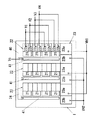
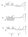
本実施形態では、イメージセンサ1として縦型オーバーフロードレインを備えるインターライン転送型CCDイメージセンサを用いる。この種のイメージセンサ1としては市場に供されているものを用いることができる。
【0039】
イメージセンサ1は、図5に示すように、感光部11となるフォトダイオード21を水平方向と垂直方向とに複数個ずつ(図示例では3×4個)配列した2次元イメージセンサであって、垂直方向に配列したフォトダイオード21の各列の右側方に垂直転送CCDからなる垂直転送部22を備え、フォトダイオード21および垂直転送部22が配列された領域の下方に水平転送CCDからなる水平転送部23を備える。垂直転送部22は各フォトダイオード21ごとに2個ずつの制御電極22a,22bを備え、水平転送部23は各垂直転送部22ごとに2個ずつの制御電極23a,23bを備える。本実施形態では、垂直転送部22を4相駆動で制御し、水平転送部23を2相駆動で制御する。つまり、垂直転送部22の制御電極22a,22bには4相の制御電圧V1〜V4を印加し、水平転送部23の制御電極23a,23bには2相の制御電圧VH1,VH2を印加する。この種の駆動技術はCCDの分野において周知であるから、ここでは詳しく説明しない。
【0040】
フォトダイオード21と垂直転送部22と水平転送部23とは1枚の基板20上に形成され、基板20の主表面には、フォトダイオード21と垂直転送部22と水平転送部23との全体を囲む形でアルミニウム電極であるオーバーフロー電極24が、基板20の全周に亘って絶縁膜を介さずに基板20に直接接触するように設けられる。オーバーフロー電極24に適宜大きさの正電圧Vsを印加すればフォトダイオード21で生成された電子(電荷)はオーバフロー電極24を通して廃棄される。つまり、本実施形態ではオーバーフロードレインの一部として基板20を用いている。オーバーフロードレインは、感光部11であるフォトダイオード21において生成した電荷のうち不要電荷を廃棄するから電荷廃棄部14として機能し、オーバーフロードレインに廃棄する電荷の量はオーバーフロー電極24に印加する電圧(廃棄電圧)により制御されるからオーバーフロー電極24は廃棄電極14aとして機能する。基板20の表面はフォトダイオード21に対応する部位を除いて遮光膜26(図6参照)により覆われる。
【0041】
イメージセンサ1について、さらに具体的に説明するために、1個のフォトダイオード21に関連する部分を切り出して図6に示す。本実施形態では、基板20にはn形半導体を用い、基板20の主表面にはフォトダイオード21と垂直転送部22とに跨る領域にp形半導体からなるpウェル31を形成している。pウェル31は、フォトダイオード21に対応する領域よりも垂直転送部22に対応する領域の厚み寸法を大きく形成してある。pウェル31のうちフォトダイオード21に対応する領域にはn+形半導体層32を重ねて設けてあり、pウェル31とn+形半導体層32とのpn接合によってフォトダイオード21が形成される。フォトダイオード21の表面にはp+形半導体からなる表面層33を積層してある。表面層33はフォトダイオード21で生成された電荷を垂直転送部22に移動させる際に、n+形半導体層32の表面付近が電荷の通過経路にならないように制御する目的で設けてある。このような構造は、埋込フォトダイオードとして知られている。
【0042】
pウェル31のうち垂直転送部22に対応する領域にはn形半導体からなる蓄積転送層34を重ねて設けてある。蓄積転送層34の表面と表面層33の表面とは略同一平面であって、蓄積転送層34の厚み寸法は表面層33の厚み寸法よりも大きくしてある。蓄積転送層34は、表面層33とは接触しているが、n+形半導体層32との間には、表面層33と不純物濃度が等しいp+形半導体からなる分離層35が介在する。蓄積転送層34の表面には、絶縁膜25を介して制御電極22a,22bが配置される。制御電極22a,22bは1個のフォトダイオード21に対して2個ずつ設けられ、垂直方向において2個の制御電極22a,22bのうちの一方は他方よりも広幅に形成される。具体的には、図7のように、1個のフォトダイオード21に対応する2個の制御電極22a,22bのうち狭幅の制御電極22bは平板状に形成されており、広幅の制御電極22aは、幅狭の制御電極22bと同一平面上に配列され一対の制御電極22bの間に配置される平板状の部分と、平板状の部分の垂直方向(図7の左右方向)における両端部からそれぞれ延長され制御電極22bの上に重複する湾曲した部分とを備える。ここに、絶縁膜25はSiO2 により形成され、また制御電極22a,22bはポリシリコンにより形成され、各制御電極22a,22bは絶縁膜25を介して互いに絶縁されている。さらに、フォトダイオード21に光を入射させる部位を除いてイメージセンサ1の表面は遮光膜26により覆われる。pウェル31において垂直転送部22に対応する領域および蓄積転送層34は垂直転送部22の全長に亘って形成され、したがって、蓄積転送層34には広幅の制御電極22aと狭幅の制御電極22bとが交互に配列されることになる。
【0043】
次に、上述したイメージセンサ1を駆動する技術について説明する。上述したイメージセンサ1では、フォトダイオード21に光が入射すれば感光部11であるフォトダイオード21において電荷が生成される。また、フォトダイオード21で生成された電荷のうち垂直転送部22に信号電荷として引き渡される電荷の割合は、制御電極22aに印加する制御電圧と廃棄電極14aであるオーバーフロー電極24に印加する廃棄電圧との関係によって決めることができる。具体的には、制御電極22aに印加する制御電圧に応じて蓄積転送層34に形成されるポテンシャル井戸の深さおよび制御電圧を印加する時間と、オーバーフロー電極24に印加する廃棄電圧に応じて廃棄電極14aに応じて形成されるフォトダイオード21と基板20との間の電位勾配および廃棄電圧を印加する時間との関係によって、垂直転送部22に引き渡される電荷の割合が決まる。制御電圧と廃棄電圧との制御は第1実施形態〜第3実施形態に記載したいずれかの技術を用いる。ただし、本実施形態では、第1実施形態と同様に、制御電極22aに制御電圧を印加する期間の一部が廃棄電極14aに廃棄電圧を印加する期間に重複するように制御する場合を想定する。
【0044】
垂直転送部22は、個々の制御電極22a,22bに印加する制御電圧を制御することによってフォトダイオード21で生成された電荷が引き渡されるだけではなく、制御電圧に応じて各制御電極22a,22bに対応する部位にポテンシャル井戸を形成する。つまり、垂直転送部22は蓄積転送層34に絶縁膜25を介して制御電極22a,22bを配置しているから、制御電極22a,22bに制御電圧を印加することによって蓄積転送部34にポテンシャル井戸を形成するのであって、ポテンシャル井戸の深さおよび幅で決まる容量の範囲内で信号電荷の蓄積が可能になる。このように、ポテンシャル井戸は信号電荷を蓄積する電荷蓄積部として機能する。また、垂直転送部22では、制御電圧の大きさおよびタイミングを変化させることによって、蓄積された信号電荷を水平転送部23に送り出すことができる。垂直転送部22から水平転送部23に送り出された信号電荷は、水平転送部23を転送されて外部に評価部5(図1参照)に取り出される。つまり、垂直転送部22および水平転送部23は電荷取出部として機能する。
【0045】
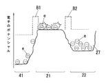
いま、フォトダイオード21で生成された電荷がどのように移動するかを説明するために、図6中の破線L1に沿った電子のポテンシャルを図8に示す。すなわち、図8における中央部はフォトダイオード21に相当する領域、左部は基板20(オーバーフロードレイン)に相当する領域、右部は垂直転送部22に相当する領域をそれぞれ示す。また、オーバーフロー電極24に電圧を印加していない状態では、フォトダイオード21と基板20との間にはpウェル31によるポテンシャル障壁B1が形成され、フォトダイオード21と垂直転送部22との間には分離層35によるポテンシャル障壁B2が形成される。ポテンシャル障壁B1,B2を破線で示しているのは、これらのポテンシャル障壁B1,B2の高さが可変であるからである。つまり、制御電極22a,22bへの印加電圧によってポテンシャル障壁B2の高さを制御することができ、オーバーフロー電極24への印加電圧によってポテンシャル障壁B1の高さを制御することができる。
【0046】
制御電極22aへの制御電圧V1とオーバーフロー電極24への廃棄電圧Vsとの印加状態と、フォトダイオード21で生成された電荷の移動との関係を図9に示す。図9(a)は制御電極22aに比較的高い正電圧の制御電圧V1を印加することにより分離層35によるポテンシャル障壁B2を取り除き、蓄積転送部34にポテンシャル井戸27を形成した状態である。この期間には、ポテンシャル障壁B1が形成されるように、オーバーフロー電極24に比較的低い廃棄電圧Vsを印加する。つまり、ポテンシャル障壁B1が存在することによって、フォトダイオード21で生成された電荷(電子e)は基板20に移動できない状態であって、この期間には、フォトダイオード21で生成された電荷は、ポテンシャル井戸27の容量が許す限り信号電荷として垂直転送部22に移動する。
【0047】
一方、図9(b)は図9(a)のように制御電極22aに比較的高い正電圧の制御電圧V1を印加した状態で、オーバーフロー電極24にも比較的高い正電圧の廃棄電圧Vsを印加した状態であって、基板20のポテンシャルを垂直転送部22のポテンシャルよりも低くなるようにオーバーフロー電極24に印加する廃棄電圧Vsを設定してある。この状態では、pウェル31によるポテンシャル障壁B1がほぼ除去され、フォトダイオード21に対する基板20の電位勾配が、フォトダイオード21に対する垂直転送部22の電位勾配よりも大きくなるから、フォトダイオード21で生成された電荷の多くは、図9(b)に矢印で示すように、不要電荷として基板20に移動し廃棄されることになる。つまり、フォトダイオード21で生成された電荷のうち信号電荷となる割合が図9(a)の状態よりも大幅に低減するから、感光部11の感度が実質的に低下したことになる。ここに、信号電荷と不要電荷との割合つまり感度は、制御電極22aとオーバーフロー電極24とに印加する電圧の大小関係によって決まるのであって、電子のポテンシャルのより低いほうにより多くの電荷(電子)が移動することになる。なお、図9(a)の状態で垂直転送部22に移動した電荷はフォトダイオード21よりもポテンシャルの低いポテンシャル井戸27に蓄積されているから、図9(b)の状態において基板20には移動しない。
【0048】
垂直転送部22に蓄積された信号電荷を読み出すには、図9(c)のように、ポテンシャル障壁B2が生じるように、制御電極22aへの制御電圧V1の印加を遮断する(比較的低い制御電圧V1を印加してもよい)。また、図示例ではこの期間においてポテンシャル障壁B1が形成されるように、オーバーフロー電極24に比較的低い廃棄電圧Vsを印加している。ただし、ポテンシャル障壁B1は必須ではなく、ポテンシャル障壁B2が形成されていればよい。ポテンシャル障壁B2を形成することによって、フォトダイオード21から垂直転送部22への電荷の流入を禁止し、かつ垂直転送部22からフォトダイオード21への電荷の流出を禁止する。この状態で、垂直転送部22に蓄積された信号電荷を水平転送部23を通して評価部5に読み出す。
【0049】
垂直転送部22に蓄積された信号電荷は、上述した4個の検出値A0,A1,A2,A3のうちの各1個の検出値A0,A1,A2,A3が求められるたびに読み出される。たとえば、検出値A0に相当する信号電荷が各フォトダイオード21に対応して形成されるポテンシャル井戸27に蓄積されると信号電荷を読み出し、次に検出値A1に相当する信号電荷がポテンシャル井戸27に蓄積されると再び信号電荷を読み出すという動作を繰り返す。なお、各検出値A0,A1,A2,A3を蓄積する期間は等しく設定しておくのはもちろんのことである。また、各検出値A0,A1,A2,A3を読み出す順序は上述の例に限定されるものではなく、検出値A0の次に検出値A2を求めるなどとしてもよい。他の構成および動作は第1実施形態と同様である。
【0050】
(第5実施形態)
本実施形態では、市場に供されている横型オーバーフロードレインを備えるインターライン転送型CCDをイメージセンサ1に用いる例を示す。
【0051】
本実施形態に用いるイメージセンサ1は、図10に示すように、垂直方向に配列したフォトダイオード21の各列の左側方にn形半導体からなる電荷廃棄部14としてのオーバーフロードレイン41を設けてある。図示例ではフォトダイオード21を水平方向に3個並べるとともに垂直方向に4個並べているから、オーバーフロードレイン41は3列であり、各オーバーフロードレイン41の上端同士は、左右方向に配置したアルミニウム電極であるオーバーフロー電極24を介して接続してある。垂直転送部22および水平転送部23は第4実施形態において用いたイメージセンサ1と同様の機能を有する。
【0052】
1個のフォトダイオード21に関連する部分を切り出した図11を用いてイメージセンサ1の構造を説明する。本実施形態ではp形半導体の基板40を用いており、基板40の主表面においてフォトダイオード21に対応する領域には、基板40とともにフォトダイオード21を形成するn+形半導体層42が重ねて形成され、基板40の主表面において垂直転送部22に対応する領域にはn形半導体からなる蓄積転送層44が重ねて形成されている。n+形半導体層42と蓄積転送層44との間にはp+形半導体からなる分離層45aが形成され、n+形半導体層42に対して蓄積転送層44とは反対側にはp+形半導体からなる分離層45bを介してオーバーフロードレイン41が設けられる。n+形半導体層42と両分離層45a,45bとに跨る部位の表面には、フォトダイオード21で生成された電荷を垂直転送部22に移動させる際に、n+形半導体層42の表面付近を電荷が通らないように制御する目的で、不純物濃度が分離層45a,45bと等しいp+形半導体からなる表面層43を積層してある。蓄積転送層44の表面と表面層43の表面とオーバフロードレイン41の表面とは略同一平面になっている。また、オーバーフロードレイン41はn+形半導体層42よりも深い位置まで基板40内に入り込んでいる。
【0053】
蓄積転送層44の表面には、絶縁膜25を介して制御電極22a,22bが配置される。制御電極22a,22bは1個のフォトダイオード21に対して2個ずつ設けられ、垂直方向において2個の制御電極22a,22bのうちの一方は他方よりも広幅に形成される。さらに、フォトダイオード21に光を入射させる部位を除いてイメージセンサ1の表面は遮光膜26により覆われる。これらの構造については第4実施形態に用いたイメージセンサ1と同様である。
【0054】
本実施形態の動作は基本的には第4実施形態と同様であって、図11の破線L2に沿った電子のポテンシャルを示している図12および図13を図8および図9と比較すればわかるように、フォトダイオード21において生成された廃棄電荷が、第4実施形態では基板20を通っていたのに対して本実施形態では基板20を通らずにオーバーフロードレイン41を通る点で相違する。
【0055】
本実施形態においてイメージセンサ1として用いた横型オーバーフロードレインを備えるインターライン転送型CCDのフォトダイオード21に用いるn+形半導体層42は、第4実施形態において用いた縦型オーバーフロードレインを備えるインターライン転送型CCDのフォトダイオード21を構成するn+形半導体層32に比較すると深さ寸法を大きくとることが可能になる。つまり、縦型オーバーフロードレインを設ける場合にはフォトダイオード21を基板20の上に形成する必要があったのに対して、横型オーバーフロードレインを設ける場合には基板40がフォトダイオード21を形成する一方の半導体層になるから、全体の厚み寸法に対して深さ方向におけるn+形半導体層42の割合を大きくとることが可能になるのである。このように、フォトダイオード21を形成するn+形半導体層42の深さ寸法を大きくとることができるから、オーバーフロードレイン41がフォトダイオード21に並設されることによって受光面積が第4実施形態よりも減少するものの、第4実施形態に比較すると近赤外線に対する感度が比較的高くなるという利点が生じる。他の構成および機能は第4実施形態と同様である。
【0056】
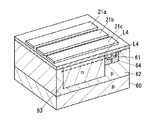
(第6実施形態)
本実施形態は、イメージセンサ1として、市場に供されている縦型オーバーフロードレインを備えるフレーム転送型CCDを用いるものである。
【0057】
イメージセンサ1は、図14に示すように、感光部11であるフォトダイオード21を水平方向と垂直方向とに複数個ずつ(図示例では4×4個)配列した2次元イメージセンサであって、垂直方向に配列したフォトダイオード21を垂直転送CCDとして機能させる撮像部D1を備え、さらに光電変換機能を持たない垂直転送CCDをフォトダイオード21の各列に垂直方向において連続して形成した蓄積部D2を備える。また、蓄積部D2における垂直転送CCDの各列の下端に電荷取出部となる水平転送CCDからなる水平転送部23を設けてある。本実施形態では、フォトダイオード21と垂直転送CCDとがともに電荷を蓄積しかつ電荷を垂直方向に転送する機能を有するのであって、撮像部D1と蓄積部D2とが電荷蓄積部12および電荷取出部13として機能する。
【0058】
各フォトダイオード21はそれぞれ垂直方向に配列された3個ずつの制御電極21a〜21cを受光面に備え、蓄積部D2における垂直転送CCDの各列は各フォトダイオード21に設けた3個の制御電極21a〜21cと同様の配列を有する3個の制御電極28a〜28cを組にして備える。図示例では撮像部D1において垂直方向の1列について4個ずつのフォトダイオード21を設け、蓄積部D2おいて2組6個の制御電極28a〜28cを設けてある。また、水平転送部23は、第4実施形態と同様に、各列ごとに2個ずつの制御電極23a,23bを備える。フォトダイオード21に設けた制御電極21a〜21cは6相の制御電圧V1〜V6により6相で駆動され、制御電極28a〜28eは3相の制御電圧VV1〜VV3により3相で駆動され、制御電極23a,23bは2相の制御電圧VH1,VH2により2相で駆動される。水平転送部23では蓄積部D2から1水平ラインごとの信号電荷を取り出し、1水平ラインごとの信号電荷を外部に出力する。この種の駆動技術はCCDの分野において周知であるから、ここでは詳しく説明しない。
【0059】
撮像部D1と蓄積部D2と水平転送部23とは1枚の基板50上に形成され、基板50にはアルミニウム電極であるオーバーフロー電極24が絶縁膜を介さずに直接接触するように設けられる。つまり、基板50はオーバーフロードレインとして機能する。オーバーフロー電極24は、基板50の表面において撮像部D1と蓄積部D2と水平転送部23との全体を囲むように形成される。基板50の表面はフォトダイオード21に対応する部位を除いて遮光膜(図示せず)により覆われる。
【0060】
図15に基づいて1個のフォトダイオード21に関連する部分の構造を説明する。本実施形態では、基板50としてn形半導体を用いており、基板50の主表面にはp形半導体層51が形成され、p形半導体層51の主表面にはn形半導体からなるnウェル52が形成される。さらに、p形半導体層51とnウェル52とに跨る部位の表面にはSiO2 からなる絶縁膜53を介して3個の制御電極21a〜21cが重ねられる。つまり、本実施形態では、nウェル52と絶縁膜53と制御電極21a〜21cとによりMIS形のフォトダイオード21を形成している。制御電極21a〜21cはポリシリコンにより形成される。nウェル52は撮像部D1と蓄積部D2とに連続して形成されており、nウェル52において電荷の蓄積と転送とを行うようにしている。つまり、撮像部D1ではnウェル52において電荷の生成と蓄積と転送とを行い、蓄積部D2ではnウェル52において電荷の蓄積と転送とを行う。
【0061】
次に、上述したイメージセンサ1を駆動する技術について説明する。上述したイメージセンサ1では、フォトダイオード21に光が入射すればフォトダイオード21において電荷が生成される。ここで、制御電極21a〜21cに適宜の電圧を印加しておけば、nウェル52に電荷蓄積部としてのポテンシャル井戸が形成され、生成された電荷をポテンシャル井戸に蓄積することができる。また、制御電極21a〜21cに印加する電圧を制御することによって、ポテンシャル井戸の深さを変化させて電荷を転送することができる。一方、オーバーフロー電極24に適宜の廃棄電圧Vsを印加すれば、フォトダイオード21で生成された電荷は基板50を通して廃棄されるから、オーバーフロー電極24への印加電圧および電圧を印加する時間を制御することによって、フォトダイオード21で生成された電荷のうちnウェル52のポテンシャル井戸に蓄積される信号電荷の割合を変化させることができる。
【0062】
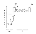
フォトダイオード21で生成された電荷がどのように移動するかを説明するために、図15中の破線L3に沿った電子のポテンシャルを図16に示す。図16における右部はフォトダイオード21に相当する領域、左部は基板50に相当する領域をそれぞれ示す。また、オーバーフロー電極24に電圧を印加していない状態では、フォトダイオード21(nウェル52)と基板50との間にはp形半導体層51によるポテンシャル障壁B3が形成される。フォトダイオード21(nウェル52)において基板50と対向していない部位にはp形半導体層51によるポテンシャル障壁B4が形成され、フォトダイオード21により形成された電荷(電子e)が外部に漏れ出さないようになっている。ポテンシャル障壁B3はオーバーフロー電極24への印加電圧に応じて高さを制御することができる。
【0063】
一方、制御電極21a〜21cに電圧を印加することによりnウェル52に形成されるポテンシャル井戸に蓄積される電荷の量は、制御電極21a〜21cへの印加電圧によって決まるポテンシャル井戸の深さによって決まる。つまり、3個の制御電極21a〜21cのうち中央の制御電極21bに印加する電圧を両側の制御電極21a,21cに印加する電圧よりも高くすると、図17(a)のように中央部がもっとも深くなったポテンシャル井戸27が形成される。ここで、オーバーフロー電極24に適宜の電圧を印加することにより、基板50のポテンシャルをnウェル52よりも引き下げ、さらに、図18(a)〜(c)のように、中央の制御電極21bはポテンシャル障壁B3が残るように電圧を印加し、両側の制御電極21a,21cはポテンシャル障壁B3が取り除かれるように電圧を印加すれば、各制御電極21a〜21cに対応する領域のうち図18(b)に示す中央部で電子eがもっとも多く蓄積され、図18(a)(c)に示す両側部では電荷が基板50を通して廃棄されることになる。
【0064】
ここで、中央の制御電極21bに対応するポテンシャル井戸27には、フォトダイオード21が電荷を生成している期間において、両側の制御電極21a,21cで生成された電荷の一部が流れ込むから、制御電極21a,21cで生成された一部の電荷が雑音成分として混ざり込むことになる。また、4個の検出値A0,A1,A2,A3のうちの1個が得られるたびに信号電荷を転送するから、信号電荷の転送中にフォトダイオード21で生成される電荷が検出値A0,A1,A2,A3に雑音成分として混入することになる。ただし、これらの雑音成分は積分によって平均化され、位相差ψを求める際の減算によってほぼ除去されるから、雑音成分の影響は小さくなる。つまり、フレーム転送型CCDを用いながらも精度よく位相差ψを求めることが可能になる。
【0065】
なお、上述の例では1個のフォトダイオード21に対して3個の制御電極21a〜21cを対応させているが、1個のフォトダイオード21に対応させる制御電極の個数にはとくに制限はない。他の構成および動作は第4実施形態と同様である。
【0066】
(第7実施形態)
本実施形態は、第6実施形態と同様にフレーム転送型CCDを用いるものであるが、縦型オーバーフロードレインではなく横型オーバーフロードレインを設けている。
【0067】
本実施形態に用いるイメージセンサ1は、図19に示すように、垂直方向に配列したフォトダイオード21の各列の右側方にn形半導体からなるオーバーフロードレイン61を設けてある。図示例ではフォトダイオード21を水平方向に4個並べるとともに垂直方向に4個並べているから、オーバーフロードレイン61は4列であり、各オーバーフロードレイン61の上端同士は、左右方向に配置したアルミニウム電極であるオーバーフロー電極24を介して接続してある。撮像部D1と蓄積部D2と水平転送部23とは第6実施形態において用いたイメージセンサ1と同様の機能を有する。
【0068】
1個のフォトダイオード21に関連する部分を切り出した図20を用いてイメージセンサ1の構造を説明する。本実施形態ではp形半導体の基板60を用いており、基板60の主表面にはp形半導体層62が形成され、このp形半導体層62にn形半導体からなるnウェル63が形成され、p形半導体層62とnウェル63とによりフォトダイオード21が形成される。p形半導体層62においてnウェル63に隣接する部位にはp+半導体からなるp+ウェル64が形成され、p+ウェル64の表面側にn形半導体からなるオーバーフロードレイン61が形成される。このように基板60の導電形が異なる点、オーバーフロードレイン61を設けている点を除けば、イメージセンサ1の基本的な構造は第6実施形態と同様である。
【0069】
本実施形態の動作は第6実施形態と同様であって、図20の破線L4に沿った電子のポテンシャルを示している図21を図16と比較すればわかるように、フォトダイオード21において生成された電荷を廃棄する電荷廃棄部が、第6実施形態では基板50であったのに対して本実施形態ではオーバーフロードレイン61である点のみ相違する。制御電極21a〜21cに電圧を印加することによりnウェル63に形成されるポテンシャル井戸に蓄積される電荷の量は、制御電極21a〜21cへの印加電圧によって決まるポテンシャル井戸の深さによって決まる。つまり、3個の制御電極21a〜21cのうち中央の制御電極21bに印加する電圧を両側の制御電極21a,21cに印加する電圧よりも高くすると、中央の制御電極21bに対応するポテンシャル井戸がもっとも深くなる。ここで、オーバーフロー電極24に適宜の電圧が印加されてポテンシャル障壁B3が引き下げられているとすれば、図18(a)〜(c)のように、中央の制御電極21bに対応するポテンシャル井戸に電荷を残し、両側の制御電極21a,21cに対応する領域で生成された電荷はオーバーフロードレイン61に廃棄することが可能になる。他の構成および動作は第6実施形態と同様である。
【0070】
(第8実施形態)
第6実施形態および第7実施形態において説明したフレーム転送型CCDをイメージセンサ1に用いる構成において、各フォトダイオード21には3個の制御電極21a〜21cを設ける例を示したが、上述のように1個のフォトダイオード21に設ける制御電極の個数は3個に制限されるものではない。
【0071】
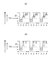
本実施形態では、1個のフォトダイオード21に対して4個の制御電極を設ける場合について説明する。図23において1〜4の数字は各制御電極に対応しており、繰り返して表記している1〜4の数字の1回の繰り返し周期が1個のフォトダイオード21の領域に対応する。図23(a)はフォトダイオード21で生成した電荷を蓄積する期間、図23(b)は不要な電荷を廃棄する期間を示している。さらに、閾値Th1はオーバーフロードレインのポテンシャルを示している。
【0072】
図23(a)に示すように、電荷を蓄積する期間においては、各フォトダイオード21で生成された電荷が混合されないように、制御電極(1)には電圧を印加せずに隣合うフォトダイオード21の間にポテンシャル障壁を形成する。また、制御電極(2)〜(4)に印加する電圧を段階的に低くし、階段状のポテンシャル井戸27を形成する。ここで、制御電極(3)(4)に対応する部位のポテンシャルは閾値Th1よりも高くしておく。制御電極(2)に対応する部位ではポテンシャル井戸27がもっとも深くなり、ポテンシャルが閾値Th1よりも低くなるから、フォトダイオード21への光の照射により生成された電荷(電子e)は、主として制御電極(2)に対応する部位に蓄積される。
【0073】
図23(b)に示すように、電荷を廃棄する廃棄期間においては、蓄積期間においてポテンシャルがもっとも低い制御電極(2)に対応する部位に蓄積された電荷が外部に漏出しないように、制御電極(3)(4)に対応する部位のポテンシャルを引き上げる。この動作によって、蓄積期間において制御電極(1)(3)(4)に対応して生成された電荷は制御電極(2)に対応する部位とオーバーフロードレインとに分かれて流れる。したがって、電荷の蓄積期間と廃棄期間との比率を適宜に調節することにより、フォトダイオード21で生成される電荷のうち不要電荷となる電荷の量を調節することができ、結果的に感度を調節することができる。他の構成および動作は第6実施形態または第7実施形態と同様である。
【0074】
(第9実施形態)
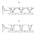
本実施形態は、図24に示すように、1個のフォトダイオード21に対して6個の制御電極(1)〜(6)を設けた例である。図24において1〜6の数字は各制御電極に対応している。図23に示した例と同様に、図24(a)は電荷を蓄積する期間、図24(b)は電荷を廃棄する期間を示している。
【0075】
図24(a)に示すように、電荷を蓄積する期間においては、各フォトダイオード21で生成された電荷が混合されないように、制御電極(1)には電圧を印加せずに隣合うフォトダイオード21の間にポテンシャル障壁を形成する。また、制御電極(2)〜(6)のうち制御電極(4)に対応する部位のポテンシャルをもっとも低くし、残りの制御電極(2)(3)(5)(6)に対応する部位のポテンシャルは段階的に高くする。さらに、制御電極(2)(3)(5)(6)に対応する部位のポテンシャルはオーバーフロードレインのポテンシャルである閾値Th2よりも高くしておく。制御電極(4)に対応する部位ではポテンシャルがもっとも低くなり、このポテンシャルは閾値Th2よりも低いから、フォトダイオード21への光の照射により生成された電荷(電子e)は、主として制御電極(4)に対応する部位に蓄積される。
【0076】
図24(b)に示すように、電荷を廃棄する期間においては、蓄積期間においてポテンシャルがもっとも低い制御電極(4)に対応する部位に蓄積された電荷が外部に漏出しないように、制御電極(2)(3)(5)(6)に対応する部位のポテンシャルを引き上げる。この動作によって、蓄積期間において制御電極(1)(2)(3)(5)(6)に対応して生成された電荷は制御電極(4)に対応する部位とオーバーフロードレインとに分かれて流れる。したがって、本実施形態でも第8実施形態と同様に、電荷の蓄積期間と廃棄期間との比率を適宜に調節することにより、フォトダイオード21で生成される電荷のうち不要電荷となる電荷の量を調節することができ、結果的に感度を調節することができる。他の構成および動作は第6実施形態または第7実施形態と同様である。
【0077】
(第10実施形態)
上述したように、フレーム転送型CCDを用いると、検出値A0,A1,A2,A3を求める期間以外にフォトダイオード21で生成された電荷が雑音成分として信号電荷に混入する。このような雑音成分は略一定であり、かつ検出値A0,A1,A2,A3を求める期間において電荷を蓄積することによって平均化されるから、位相差を求めることができる程度には雑音成分を除去することが可能である。しかしながら、雑音成分があるとSN比が低下するから、電荷の蓄積や転送に関連する部位ではダイナミックレンジを大きくとることが要求され、結果的に高コストになる。
【0078】
そこで、本実施形態では、図25に示すように、フォトダイオード21のうち信号電荷を蓄積する領域付近と電荷の生成に関与しない領域とに遮光膜65を設けている。図示例は第9実施形態のように1個のフォトダイオード21に対して6個の制御電極を設けた場合の構成例であって、具体的には、制御電極(1)(4)に対応する部位に遮光膜65を設けることによって、フォトダイオード21のうち制御電極(2)(3)(5)(6)に対応する部位で電荷(電子e)を生成するようにしている。この構成によって、主として制御電極(2)(3)(5)(6)に対応する部位で電荷の生成が行われ、制御電極(4)が電荷の生成にはほとんど寄与しなくなる。つまり、制御電極(4)において雑音成分が生成されず、遮光膜65を形成していない場合に比較するとSN比を向上させることが可能になる。他の構成および機能は第9実施形態と同様である。
【0079】
なお、第4実施形態ないし第10実施形態において、制御電圧と廃棄電圧との制御タイミングとして第1実施形態の技術を適用する例について説明したが、第2実施形態、第3実施形態の技術を適用してもよいのはもちろんのことである。
【0080】
上述した各実施形態では、4個の検出値A0,A1,A2,A3のうちの1個を求めるたびに電荷を取り出す構成を採用していたが、以下に説明するイメージセンサ1では、複数個の検出値A0,A1,A2,A3を求めてから一括して取り出すことを可能にしたものである。
【0081】
(第11実施形態)
本実施形態は、図19に示した横型オーバーフロードレインを備えるフレーム転送型CCDの一部構成を変更したイメージセンサ1を用いる。すなわち、図26に示すように、各フォトダイオード21ごとにオーバーフロードレイン61a,61bを設けた構成を採用し、各フォトダイオード21で生成した電荷を個別に廃棄することを可能としている。この構成では、各オーバーフロードレイン61a,61bに変調信号の周期に同期した廃棄電圧を印加することによって、フォトダイオード21で生成された電荷のうち電荷蓄積部であるポテンシャル井戸に移動する信号電荷の割合を調節する。ただし、本実施形態では、各オーバーフロードレイン61a,61bのうち、信号電荷を転送する方向において隣接する各一対のオーバーフロードレイン61a,61bに廃棄電圧φ1,φ2を印加するタイミングは、変調信号において位相が180度異なるタイミングとする。2個の感光部11に対して位相が180度異なるタイミングで廃棄電圧φ1,φ2を印加することによって、変調信号において位相が180度異なるタイミングに対応した信号電荷を各感光部11に対応して形成されるポテンシャル井戸に蓄積することができる。つまり、隣接した2個の感光部11にそれぞれ形成されるポテンシャル井戸に変調信号における異なる位相に対応した信号電荷を蓄積することができ、位相差ψを求めるのに必要な4個の検出値A0,A1,A2,A3のうちの2個を一括して取り出すことが可能になる。このようにして、検出値A0と検出値A2とを一括して取り出し、検出値A1と検出値A3とを一括して取り出すことが可能になる。
【0082】
本実施形態の構成では、信号電荷に対して目的外の電荷が混在するから雑音成分が生じるものの、雑音成分は信号電荷の量に比較すると少なく、また信号電荷に対して略一定の割合で混在するから、位相差ψを求める際には雑音成分の影響は低減される。他の構成および動作は第7実施形態と同様である。
【0083】
(第12実施形態)
第11実施形態では、フレーム転送型CCDを用いているが、図27に示すように、横型オーバーフロードレインを用いたインターライン転送型CCDを用いることによっても同様の動作が可能である。つまり、図10に示した第5実施形態の構成において、各フォトダイオード21ごとにオーバーフロードレイン41a,41bを分割して設けた構成のイメージセンサ1を用い、さらに垂直転送部22においては、各フォトダイオード21ごとに3個ずつの制御電極22a〜22cを設ければよい。この構成のイメージセンサ1において、垂直方向に隣接するオーバフロードレイン41a,41bに対して変調信号における異なる位相の廃棄電圧を与え、また各制御電極22a〜22bについては、第11実施形態における制御電極(1)〜(6)と同様に6相の制御電圧で駆動すれば、検出値A0,A1,A2,A3を2個ずつ求めることが可能になる。他の構成および動作は第11実施形態と同様である。
【0084】
第11実施形態ではオーバーフロードレイン61a,61bごとに3個ずつの制御電極21a〜21cを対応付け、第12実施形態ではオーバフロードレイン41a,41bごとに3個ずつの制御電極22a〜22cを対応付けているが、それぞれ4個以上設けるようにしてもよい。また、変調信号の位相において180度異なるタイミングの廃棄電圧φ1,φ2を異なるオーバフロードレインに与える構成を採用しているが、たとえば変調信号において90度ずつ位相の異なるタイミングで廃棄電圧を互いに異なるオーバフロードレインに与える構成とすれば、4個の検出値A0,A1,A2,A3を一括して取り出すことも可能である。さらに、廃棄電圧を印加するタイミングは、変調信号の周期に同期した特定の位相であればよく、間隔は適宜に設定可能である。
【0085】
上述した各実施形態では、インターライン転送型CCDあるいはフレーム転送型CCDを用いる例を示したが、図28に示すように、図14に示したフレーム転送型CCDの撮像部D1をインターライン転送型CCDのフォトダイオード21と垂直転送部22とに置換した構成のフレームインターライン転送CCDを用いることも可能である。この構成のイメージセンサ1は、フレーム転送型CCDに比較するとスミアの発生を抑制することができる。
【0086】
【発明の効果】
請求項1の発明の構成によれば、廃棄電極を備え感光部で生成した電荷のうち不要電荷として廃棄する電荷の割合が廃棄電極に印加する廃棄電圧に応じて増減する電荷廃棄部を備え、かつ廃棄電極に印加する廃棄電圧を変調信号の周期に同期するタイミングで変化させるから、感光部で生成された電荷のうち信号電荷として使用しない残留電荷は不要電荷として廃棄され、信号電荷への雑音成分の混入が抑制されるという利点がある。とくに、廃棄電圧を変調信号の周期に同期するタイミングで変化させるから、信号電荷への混入を防止したい不要電荷を的確に廃棄することができ、SN比の向上につながる。また、不要電荷となる残留電荷を迅速に除去しているから、残留電荷の再結合による自然消滅を待つまでもなく比較的短い時間間隔で信号電荷を取り出すことが可能になる。
【0087】
請求項2の発明の構成によれば、制御電圧を一定電圧に保っているから、制御が容易である。
【0088】
請求項3の発明の構成によれば、感光部で生成した電荷のうち電荷蓄積部に蓄積する信号電荷の割合を、制御電極に印加する制御電圧と廃棄電極に印加する廃棄電圧との両方により制御するから、感光部で生成された電荷のうち信号電荷として必要な電荷を電荷蓄積部に転送しながらも、感光部で生成された電荷のうち信号電荷として使用しない残留電荷は不要電荷として廃棄することができ、信号電荷への雑音成分の混入が抑制されるという利点がある。
【0089】
請求項4の発明の構成によれば、感光部で生成した電荷のうち電荷蓄積部に蓄積する信号電荷の割合を制御電極に印加する制御電圧により制御するから、感光部で生成された電荷のうち信号電荷として必要な電荷を電荷蓄積部に転送することができ、しかも廃棄電極に印加する廃棄電圧は一定電圧に保っているから、感光部で生成された電荷のうち信号電荷として使用しない残留電荷は不要電荷として廃棄することができ、結果的に信号電荷への雑音成分の混入が抑制されるという利点がある。また、残留電荷を迅速に除去しているから、残留電荷の再結合による自然消滅を待つまでもなく比較的短い時間間隔で信号電荷を取り出すことが可能になる。
【0090】
請求項5の発明の構成によれば、オーバーフロードレインを有した既製のCCDイメージセンサを用いて実現することができる。
【0091】
請求項6の発明の構成によれば、複数の位相に対応した信号電荷を1個の感光部を共用して検出する場合のように各位相の信号電荷を得るたびに電荷集積部に信号電荷を取り出す必要がなく、必要な個数の信号電荷が得られた後に電荷集積部に一括して信号電荷を取り出すことができる。つまり、感光部から電荷集積部への信号電荷の取出頻度を低減することができる。
【0092】
請求項7の発明の構成によれば、電荷蓄積部の近傍では光の入射に伴う電荷の生成が少なく、信号電荷への雑音成分の混入が少ないという利点がある。
【0093】
請求項8の発明の構成によれば、発光源から照射した光と感光部で受光した光との位相差を求めるから、空間情報として位相差によって表される情報、たとえば物体までの距離を求めることが可能になる。
【0094】
請求項9の発明の構成によれば、上述した各請求項の効果を持つ測距装置を提供することができる。
【図面の簡単な説明】
【図1】第1実施形態を示すブロック図である。
【図2】同上の動作説明図である。
【図3】第2実施形態を示す動作説明図である。
【図4】第3実施形態を示す動作説明図である。
【図5】第4実施形態に用いるイメージセンサを示す平面図である。
【図6】同上の要部分解斜視図である。
【図7】図6のA−A線断面図である。
【図8】同上の動作説明図である。
【図9】同上の動作説明図である。
【図10】第5実施形態に用いるイメージセンサを示す平面図である。
【図11】同上の要部分解斜視図である。
【図12】同上の動作説明図である。
【図13】同上の動作説明図である。
【図14】第6実施形態に用いるイメージセンサを示す平面図である。
【図15】同上の要部斜視図である。
【図16】同上の動作説明図である。
【図17】同上の動作説明図である。
【図18】同上の動作説明図である。
【図19】第7実施形態に用いるイメージセンサを示す平面図である。
【図20】同上の要部斜視図である。
【図21】同上の動作説明図である。
【図22】同上の動作説明図である。
【図23】第8実施形態を示す動作説明図である。
【図24】第9実施形態を示す動作説明図である。
【図25】第10実施形態を示す動作説明図である。
【図26】第11実施形態を示す要部斜視図である。
【図27】第12実施形態に用いるイメージセンサを示す平面図である。
【図28】本発明の他の構成例に用いるイメージセンサを示す平面図である。
【図29】従来例を示す動作説明図である。
【符号の説明】
1 イメージセンタ
2 発光源
3 制御回路部
4 受光レンズ
5 評価部
11 感光部
12 電荷蓄積部
12a 制御電極
13 電荷取出部
14 電荷廃棄部
14a 廃棄電極
21 フォトダイオード
21a〜21c 制御電極
22 垂直転送部
22a〜22c 制御電極
23 水平転送部
24 オーバーフロー電極
40 基板
41 オーバーフロードレイン
50 基板
60 基板
61 オーバーフロードレイン[0001]
TECHNICAL FIELD OF THE INVENTION
The present invention relates to an apparatus for detecting spatial information using intensity-modulated light that detects various types of information about a space by receiving light from a space to which the intensity-modulated light is applied.
[0002]
[Prior art]
Conventionally, the light whose intensity has been modulated is emitted from the light emitting source to the space, and the reflected light reflected by the object existing in this space is received by the photosensitive unit, and the light emitted from the light emitting source and the light received by the photosensitive unit are received. There is known a technique for detecting various kinds of information about a space based on the relationship of. The information on the space means a distance to an object existing in the space, a change in the amount of received light due to reflection of the object existing in the space, and the like.
[0003]
In order to determine the distance to the object using the intensity-modulated light, the received light intensity is detected multiple times at specific different phases synchronized with the modulation cycle, which is the reciprocal of the modulation frequency. The phase difference between the light emitted from the light emitting source and the light received by the photosensitive unit is obtained from the relationship. For example, if the intensity of the light emitted from the light emitting source is modulated by a sine wave, and the light receiving intensity at the photosensitive portion for a specific different phase at the time of the modulation is detected three times or more (preferably four times or more), the phase difference is detected. You can ask.
[0004]
Now, it is assumed that the light emitted from the light emitting source is intensity-modulated as shown by a curve A in FIG. 29, and the received light intensity at the photosensitive unit changes as shown by a curve B in FIG. Here, the detected values corresponding to the respective received light intensities when the received light intensity is sampled at four points where the phase of the curve A is 0 degree, 90 degrees, 180 degrees, and 270 degrees are A0, A1, A2, and A3, respectively. . However, the detection values A0, A1, A2, and A3 in each phase do not correspond to the incident light at the instant of time in each phase, but correspond to, for example, the incident light in a period shown as an integration time Tw in the figure. Here, the phase difference ψ does not change during the sampling period of the detection values A0, A1, A2, and A3, and the change in the light attenuation rate from light emission to light reception (attenuation is ignored in the figure). If not, the detection values A0, A1, A2, and A3 are obtained at every 90 degrees. Therefore, the relationship between each detection value A0, A1, A2, and A3 and the phase difference こ と is expressed by the following equation. Can be.
ψ = tan -1 {(A3-A1) / (A0-A2)}
When the phase difference 求 め る is obtained from the plurality of detection values A0, A1, A2, and A3 as described above, the modulation period T [s], the phase difference ψ [rad], and the light speed c [m / s] are obtained. The distance L [m] to the object can be obtained using the following equation.
L ≒ cT (ψ / 4π)
As an apparatus for realizing the above technical idea, an electric switch provided with one photosensitive unit and four memory cells for one pixel and provided between each memory cell and the photosensitive unit in one pixel, It has been proposed that each detection value A0, A1, A2, A3 be sorted and accumulated in each memory cell by being turned on during a period corresponding to the integration time Tw described above (for example, see Patent Document 1). .
[0005]
[Patent Document 1]
Japanese Patent Publication No. 10-508736 (pages 7-9, FIGS. 1 and 4)
[0006]
[Problems to be solved by the invention]
By the way, in the device described in
[0007]
Here, it is assumed that the maximum distance that can be measured is, for example, 7.5 m. In this case, since the modulation frequency is 20 MHz, the integration time Tw must be shorter than the modulation period of 50 ns. On the other hand, since the time required for the residual charge to disappear by recombination is usually longer than 100 μs, not only the charge generated by light reception during the integration period Tw but also the residual charge is transferred to the memory cell. In other words, noise components due to residual charges are mixed into the charges stored in the memory cells in addition to signal charges corresponding to the detected values A0, A1, A2, and A3. Since the light received by the photosensitive unit is intensity-modulated, the noise component also changes in accordance with the detected values A0, A1, A2, and A3. Error may occur.
[0008]
The present invention has been made in view of the above circumstances, and an object of the present invention is to dispose of a noise component into a signal charge by discarding a residual charge that is not used as a signal charge among charges generated in a photosensitive unit. It is an object of the present invention to provide a spatial information detection device using intensity modulated light that suppresses spatial information and enables detection of spatial information with a high SN ratio.
[0009]
[Means for Solving the Problems]
According to the first aspect of the present invention, there is provided a photosensitive unit that receives light from a space irradiated with light intensity-modulated by a modulation signal of a predetermined modulation frequency and generates an amount of electric charge corresponding to the received light intensity; A charge storage unit for storing signal charges among generated charges, and a ratio of charges to be discarded as unnecessary charges among charges generated by the photosensitive unit, the charge discarding increasing or decreasing according to a discard voltage applied to the waste electrode. Unit, a charge extracting unit for extracting signal charges accumulated in the charge accumulating unit to the outside, a control circuit unit for changing a waste voltage applied to the waste electrode at a timing synchronized with a cycle of the modulation signal, and a charge extracting unit. An evaluation unit that evaluates information about the space using electric charges.
[0010]
According to a second aspect of the present invention, in the first aspect of the present invention, the charge storage unit increases or decreases a ratio of charges transferred to the charge storage unit among charges generated in the photosensitive unit according to a control voltage applied. Wherein the control circuit maintains the control voltage applied to the control electrode at a constant voltage.
[0011]
A third aspect of the present invention is the control electrode according to the first aspect, wherein the charge storage unit increases or decreases the ratio of the charge transferred to the charge storage unit among the charges generated in the photosensitive unit in accordance with the control voltage applied. The control circuit unit controls the control voltage to the control electrode and the waste to the waste electrode so that a period for moving the charge generated in the photosensitive unit to the charge storage unit and a period for moving the charge to the charge disposal unit alternately occur. And controlling the voltage.
[0012]
According to a fourth aspect of the present invention, there is provided a photosensitive unit that receives light from a space irradiated with light intensity-modulated by a modulation signal of a predetermined modulation frequency and generates an amount of electric charge corresponding to the received light intensity; The charge accumulating section, in which the proportion of electric charges accumulated as signal charges among the electric charges generated in the photosensitive section increases and decreases according to the control voltage applied to the control electrode, and the waste electric charge as an unnecessary charge in the electric charges generated in the photosensitive section A charge discarding unit in which the proportion of discarded charges increases or decreases according to the discard voltage applied to the discard electrode, a charge extraction unit that extracts the signal charges stored in the charge storage unit to the outside, and a fixed voltage that applies the discard voltage applied to the discard electrodes By changing the control voltage applied to the control electrode at the timing synchronized with the cycle of the modulation signal while disposing of the charge while keeping the charge, the signal charge stored in the charge storage portion of the charge generated in the photosensitive portion is changed. A control circuit unit for changing the focus, characterized in that it comprises an evaluation unit for evaluating the information related to the space using a charge removed by a charge take-out portion.
[0013]
According to a fifth aspect of the present invention, in the first to fourth aspects of the present invention, a plurality of the photosensitive portions are arranged on a main surface of the semiconductor substrate, and the charge accumulating portion and the charge extracting portion formed of a CCD are provided on the semiconductor substrate. The charge discarding section is an overflow drain provided in the CCD image sensor.
[0014]
According to a sixth aspect of the present invention, in the first to fifth aspects of the present invention, a plurality of adjacent predetermined photosensitive units among the photosensitive units are grouped, and the control circuit unit includes a plurality of photosensitive groups. The charges respectively generated in the sections are separately stored in the charge storage sections at different phase timings synchronized with the cycle of the modulation signal, and the charge extraction sections are obtained corresponding to the plurality of photosensitive sections which are a set. Each signal charge corresponding to a different phase is extracted at a time.
[0015]
According to a seventh aspect of the present invention, in the first to sixth aspects, a light-shielding film is provided on the control electrode provided in the vicinity of a region for storing signal charges in the charge storage section.
[0016]
According to an eighth aspect of the present invention, in the first to seventh aspects of the present invention, the evaluation unit determines a phase difference between the light emitted from the light emitting source to the space and the light received by the photosensitive unit when the modulation signal is different. It is characterized by being obtained from a plurality of signal charges corresponding to the phase.
[0017]
According to a ninth aspect of the present invention, in the invention of the eighth aspect, the evaluation unit converts the phase difference into a distance.
[0018]
BEST MODE FOR CARRYING OUT THE INVENTION
In each of the following embodiments, an example will be described in which the technology of the present invention is used for a distance measuring device that measures a distance using a phase difference between light from a light emitting source whose intensity is modulated and light received by a photosensitive unit. The technical idea of the present invention is not limited to the measurement of the distance, but may be applied to an apparatus for calculating a phase difference between an original phase of intensity-modulated light and light received by a photosensitive unit, an apparatus for determining a change in reflected light from an object, and the like. Is also applicable.
[0019]
(1st Embodiment)
In the present embodiment, as shown in FIG. 1, a
[0020]
On the other hand, light from the space enters the
[0021]
The
[0022]
As described in the conventional configuration, in order to obtain the distance to the object Ob, it is necessary to obtain the detection values A0, A1, A2, and A3 at timings synchronized with the cycle of the modulation signal. Of the modulated signal, a charge corresponding to a certain time width Tw (see FIG. 29) corresponding to a specific phase (for example, four phases of 0, 90, 180, and 270 degrees) of the modulation signal is set as the signal charge, It is necessary to accumulate it. That is, the ratio of the signal charge stored in the
[0023]
In order to control the sensitivity in the
[0024]
Now, it is assumed that the intensity of light emitted from the
[0025]
In the above-described control, the control voltage that is a constant voltage is applied to the
[0026]
As described above, in the present embodiment, the
[0027]
In the above-described example, the period during which the detection values A0, A1, A2, and A3 are sampled is set to 1/4 cycle of the modulation signal, and one type of detection value A0, A1, A2, and A3 is used in the tens of thousands to hundreds of thousands cycles of the modulation signal. However, when the
[0028]
(2nd Embodiment)
In the first embodiment, as shown in FIG. 2, by applying a waste voltage to the
[0029]
Here, as in the first embodiment, a case where signal charges corresponding to the detection value A0 are accumulated will be described as an example. Now, it is assumed that the intensity of light emitted from the
[0030]
In the control of the present embodiment, the period in which the control voltage is applied to the
[0031]
In the present embodiment, the period for accumulating the signal charges in the
[0032]
As described above, in the present embodiment, the
[0033]
(Third embodiment)
In the first embodiment, as shown in FIG. 2, by applying the waste voltage to the
[0034]
Also in the present embodiment, as in the first embodiment, a case where signal charges corresponding to the detection value A0 are accumulated will be described as an example. Now, it is assumed that the intensity of light emitted from the
[0035]
In the control of the present embodiment, a fixed voltage is applied to the
[0036]
As described above, in the present embodiment, the
[0037]
(Fourth embodiment)
In the embodiment described below, an example in which a CCD image sensor having an overflow drain is used as the
[0038]
In the present embodiment, an interline transfer type CCD image sensor having a vertical overflow drain is used as the
[0039]
As shown in FIG. 5, the
[0040]
The
[0041]
In order to describe the
[0042]
In a region of the p-well 31 corresponding to the
[0043]
Next, a technique for driving the above-described
[0044]
The
[0045]
Now, in order to explain how the charges generated by the
[0046]
FIG. 9 shows the relationship between the state of application of the control voltage V1 to the
[0047]
On the other hand, FIG. 9B shows a state in which a relatively high positive voltage control voltage V1 is applied to the
[0048]
To read out the signal charges stored in the
[0049]
The signal charges stored in the
[0050]
(Fifth embodiment)
In this embodiment, an example in which an interline transfer type CCD having a horizontal overflow drain provided on the market is used for the
[0051]
As shown in FIG. 10, the
[0052]
The structure of the
[0053]
The
[0054]
The operation of this embodiment is basically the same as that of the fourth embodiment. FIG. 12 and FIG. 13 showing the potential of the electrons along the broken line L2 in FIG. 11 can be compared with FIG. 8 and FIG. As can be seen, the difference is that the waste charge generated in the
[0055]
The n +
[0056]
(Sixth embodiment)
In this embodiment, a frame transfer type CCD having a vertical overflow drain provided on the market is used as the
[0057]
As shown in FIG. 14, the
[0058]
Each
[0059]
The imaging unit D1, the storage unit D2, and the
[0060]
The structure of a portion related to one
[0061]
Next, a technique for driving the above-described
[0062]
FIG. 16 shows the potential of the electrons along the broken line L3 in FIG. 15 in order to explain how the charges generated by the
[0063]
On the other hand, the amount of charge accumulated in the potential well formed in the n-well 52 by applying a voltage to the
[0064]
Here, a part of the charges generated by the
[0065]
In the above-described example, three
[0066]
(Seventh embodiment)
The present embodiment uses a frame transfer type CCD similarly to the sixth embodiment, but has a horizontal overflow drain instead of a vertical overflow drain.
[0067]
As shown in FIG. 19, the
[0068]
The structure of the
[0069]
The operation of this embodiment is the same as that of the sixth embodiment. As can be seen by comparing FIG. 21 showing the electron potential along the broken line L4 in FIG. The only difference is that the charge discarding unit for discarding the accumulated charges is the
[0070]
(Eighth embodiment)
In the configuration in which the frame transfer type CCD described in the sixth embodiment and the seventh embodiment is used for the
[0071]
In the present embodiment, a case in which four control electrodes are provided for one
[0072]
As shown in FIG. 23 (a), during the period of accumulating electric charges, no voltage is applied to the control electrode (1) so that the electric charges generated by the
[0073]
As shown in FIG. 23 (b), in the discarding period in which the electric charge is discarded, the control electrode is controlled so that the electric charge accumulated in the portion corresponding to the control electrode (2) having the lowest potential during the accumulation period does not leak outside. (3) The potential of the portion corresponding to (4) is raised. Due to this operation, the charge generated corresponding to the control electrodes (1), (3), and (4) during the accumulation period flows separately to the portion corresponding to the control electrode (2) and the overflow drain. Therefore, by appropriately adjusting the ratio between the charge accumulation period and the discard period, the amount of unnecessary charges among the charges generated by the
[0074]
(Ninth embodiment)
This embodiment is an example in which six control electrodes (1) to (6) are provided for one
[0075]
As shown in FIG. 24A, during the period of accumulating electric charges, adjacent photodiodes are applied without applying a voltage to the control electrode (1) so that the electric charges generated by the
[0076]
As shown in FIG. 24 (b), during the period of discarding the electric charge, the control electrode () is set so that the electric charge accumulated in the portion corresponding to the control electrode (4) having the lowest potential during the accumulation period does not leak outside. 2) The potential of the portion corresponding to (3), (5) and (6) is raised. By this operation, in the accumulation period, the charges generated corresponding to the control electrodes (1), (2), (3), (5), and (6) flow separately to the portion corresponding to the control electrode (4) and the overflow drain. . Therefore, in the present embodiment, similarly to the eighth embodiment, by appropriately adjusting the ratio between the charge accumulation period and the discard period, the amount of unnecessary electric charges among the electric charges generated by the
[0077]
(Tenth embodiment)
As described above, when the frame transfer type CCD is used, the charge generated by the
[0078]
Therefore, in the present embodiment, as shown in FIG. 25, the light-shielding
[0079]
In the fourth to tenth embodiments, the example in which the technology of the first embodiment is applied as the control timing of the control voltage and the waste voltage has been described. However, the technology of the second embodiment and the third embodiment is not described. Of course, it may be applied.
[0080]
In each of the above-described embodiments, the configuration is adopted in which the charge is taken out each time one of the four detection values A0, A1, A2, and A3 is obtained. The detection values A0, A1, A2, and A3 are obtained and then taken out at once.
[0081]
(Eleventh embodiment)
This embodiment uses the
[0082]
In the configuration of the present embodiment, although noise components are generated because unintended charges are mixed with signal charges, the noise components are small compared to the amount of signal charges and mixed at a substantially constant ratio with respect to signal charges. Therefore, when determining the phase difference ψ, the influence of noise components is reduced. Other configurations and operations are the same as in the seventh embodiment.
[0083]
(Twelfth embodiment)
In the eleventh embodiment, a frame transfer type CCD is used, but the same operation can be performed by using an interline transfer type CCD using a horizontal overflow drain as shown in FIG. That is, in the configuration of the fifth embodiment shown in FIG. 10, the
[0084]
In the eleventh embodiment, three
[0085]
In each of the embodiments described above, an example in which an interline transfer CCD or a frame transfer CCD is used has been described. However, as shown in FIG. 28, the imaging unit D1 of the frame transfer CCD shown in FIG. It is also possible to use a frame interline transfer CCD having a configuration in which the
[0086]
【The invention's effect】
According to the configuration of the first aspect of the present invention, a charge discarding unit is provided, which includes a discard electrode and a ratio of charges discarded as unnecessary charges among charges generated in the photosensitive unit increases or decreases according to a discard voltage applied to the discard electrode. In addition, since the waste voltage applied to the waste electrode is changed at a timing synchronized with the cycle of the modulation signal, of the charges generated in the photosensitive portion, the remaining charges not used as signal charges are discarded as unnecessary charges, and noise to the signal charges is discarded. There is an advantage that mixing of components is suppressed. In particular, since the discard voltage is changed at a timing synchronized with the cycle of the modulation signal, unnecessary charges to be prevented from being mixed into the signal charges can be discarded accurately, leading to an improvement in the SN ratio. In addition, since the residual charges, which become unnecessary charges, are quickly removed, the signal charges can be taken out at a relatively short time interval without waiting for spontaneous disappearance due to recombination of the residual charges.
[0087]
According to the configuration of the second aspect of the present invention, since the control voltage is maintained at a constant voltage, control is easy.
[0088]
According to the configuration of the third aspect of the present invention, the ratio of the signal charge stored in the charge storage unit to the charge generated in the photosensitive unit is determined by both the control voltage applied to the control electrode and the waste voltage applied to the waste electrode. Because of the control, of the charges generated in the photosensitive section, the charges required as signal charges are transferred to the charge storage section, while the remaining charges not used as signal charges among the charges generated in the photosensitive section are discarded as unnecessary charges. Therefore, there is an advantage that the noise component is prevented from being mixed into the signal charge.
[0089]
According to the configuration of the fourth aspect of the present invention, the ratio of the signal charge stored in the charge storage unit to the charge generated in the photosensitive unit is controlled by the control voltage applied to the control electrode. The charge required as signal charge can be transferred to the charge storage unit, and the waste voltage applied to the waste electrode is kept at a constant voltage. The electric charge can be discarded as unnecessary electric charge, and as a result, there is an advantage that the noise component is prevented from being mixed into the signal electric charge. Further, since the residual charges are quickly removed, the signal charges can be taken out at a relatively short time interval without waiting for spontaneous disappearance due to recombination of the residual charges.
[0090]
According to the configuration of the fifth aspect of the present invention, it can be realized using a ready-made CCD image sensor having an overflow drain.
[0091]
According to the configuration of the sixth aspect of the present invention, each time the signal charge of each phase is obtained as in the case of detecting the signal charge corresponding to a plurality of phases by sharing one photosensitive unit, the signal charge is stored in the charge accumulation unit. It is not necessary to take out the signal charges, and after the required number of signal charges have been obtained, the signal charges can be taken out at once in the charge accumulation section. That is, the frequency of taking out signal charges from the photosensitive section to the charge accumulation section can be reduced.
[0092]
According to the configuration of the seventh aspect of the present invention, there is an advantage that the generation of electric charge due to the incidence of light is small in the vicinity of the electric charge accumulating portion, and the noise component is less mixed into the signal electric charge.
[0093]
According to the configuration of the invention of claim 8, since the phase difference between the light emitted from the light emitting source and the light received by the photosensitive unit is obtained, information represented by the phase difference as the spatial information, for example, the distance to the object is obtained. It becomes possible.
[0094]
According to the configuration of the ninth aspect, it is possible to provide a distance measuring apparatus having the effects of the above-described claims.
[Brief description of the drawings]
FIG. 1 is a block diagram showing a first embodiment.
FIG. 2 is an operation explanatory view of the above.
FIG. 3 is an operation explanatory view showing a second embodiment.
FIG. 4 is an operation explanatory view showing a third embodiment.
FIG. 5 is a plan view showing an image sensor used in a fourth embodiment.
FIG. 6 is an exploded perspective view of a main part of the above.
FIG. 7 is a sectional view taken along line AA of FIG. 6;
FIG. 8 is an operation explanatory view of the above.
FIG. 9 is an operation explanatory view of the above.
FIG. 10 is a plan view illustrating an image sensor used in a fifth embodiment.
FIG. 11 is an exploded perspective view of a main part of the above.
FIG. 12 is an operation explanatory view of the above.
FIG. 13 is an operation explanatory diagram of the above.
FIG. 14 is a plan view illustrating an image sensor used in a sixth embodiment.
FIG. 15 is a perspective view of a main part of the above.
FIG. 16 is an operation explanatory view of the above.
FIG. 17 is an operation explanatory view of the above.
FIG. 18 is an explanatory diagram of the above operation.
FIG. 19 is a plan view showing an image sensor used in the seventh embodiment.
FIG. 20 is a perspective view of a main part of the above.
FIG. 21 is an explanatory diagram of the operation of the above.
FIG. 22 is an explanatory diagram of the operation of the above.
FIG. 23 is an operation explanatory view showing the eighth embodiment.
FIG. 24 is an operation explanatory view showing the ninth embodiment.
FIG. 25 is an operation explanatory view showing the tenth embodiment.
FIG. 26 is a perspective view of a principal part showing an eleventh embodiment.
FIG. 27 is a plan view showing an image sensor used in the twelfth embodiment.
FIG. 28 is a plan view showing an image sensor used in another configuration example of the present invention.
FIG. 29 is an operation explanatory view showing a conventional example.
[Explanation of symbols]
1 Image Center
2 Light source
3 Control circuit section
4 Receiving lens
5 Evaluation section
11 Photosensitive unit
12 Charge storage unit
12a Control electrode
13 Charge extraction unit
14 Charge Disposal Department
14a Waste electrode
21 Photodiode
21a-21c Control electrode
22 Vertical transfer unit
22a-22c control electrode
23 Horizontal transfer unit
24 overflow electrode
40 substrate
41 Overflow drain
50 substrates
60 substrate
61 Overflow drain
Claims (9)
Priority Applications (10)
| Application Number | Priority Date | Filing Date | Title |
|---|---|---|---|
| JP2003155712A JP3906824B2 (en) | 2003-05-30 | 2003-05-30 | Spatial information detection device using intensity-modulated light |
| KR1020047017288A KR100682566B1 (en) | 2002-07-15 | 2003-07-14 | Light receiving device with controllable sensitivity and spatial information detecting apparatus using the same |
| AU2003281107A AU2003281107A1 (en) | 2002-07-15 | 2003-07-14 | Light receiving device with controllable sensitivity and spatial information detecting apparatus using the same |
| PCT/JP2003/008934 WO2004008175A1 (en) | 2002-07-15 | 2003-07-14 | Light receiving device with controllable sensitivity and spatial information detecting apparatus using the same |
| CNB038132605A CN1312489C (en) | 2002-07-15 | 2003-07-14 | Light receiving device with controllable sensitivity and spatial information detecting apparatus using the same |
| TW092119113A TWI221730B (en) | 2002-07-15 | 2003-07-14 | Light receiving device with controllable sensitivity and spatial information detecting apparatus using the same |
| DE60319228T DE60319228T2 (en) | 2002-07-15 | 2003-07-14 | LIGHT RECEPTION DEVICE WITH REGULAR SENSITIVITY AND DEVICE FOR DETECTING SPATIAL INFORMATION THAT USES THEM |
| EP03741382A EP1521981B1 (en) | 2002-07-15 | 2003-07-14 | Light receiving device with controllable sensitivity and spatial information detecting apparatus using the same |
| US10/510,216 US7138646B2 (en) | 2002-07-15 | 2003-07-14 | Light receiving device with controllable sensitivity and spatial information detecting apparatus with charge discarding device using the same |
| HK05106915A HK1074673A1 (en) | 2002-07-15 | 2005-08-11 | Light receiving device with controllable sensitivity and spatial information detecting apparatus us ing the same |
Applications Claiming Priority (1)
| Application Number | Priority Date | Filing Date | Title |
|---|---|---|---|
| JP2003155712A JP3906824B2 (en) | 2003-05-30 | 2003-05-30 | Spatial information detection device using intensity-modulated light |
Related Child Applications (2)
| Application Number | Title | Priority Date | Filing Date |
|---|---|---|---|
| JP2006231353A Division JP3979443B2 (en) | 2006-08-28 | 2006-08-28 | Spatial information detection device using intensity-modulated light |
| JP2006231352A Division JP3979442B2 (en) | 2006-08-28 | 2006-08-28 | Spatial information detection device using intensity-modulated light |
Publications (2)
| Publication Number | Publication Date |
|---|---|
| JP2004356594A true JP2004356594A (en) | 2004-12-16 |
| JP3906824B2 JP3906824B2 (en) | 2007-04-18 |
Family
ID=34050020
Family Applications (1)
| Application Number | Title | Priority Date | Filing Date |
|---|---|---|---|
| JP2003155712A Expired - Fee Related JP3906824B2 (en) | 2002-07-15 | 2003-05-30 | Spatial information detection device using intensity-modulated light |
Country Status (1)
| Country | Link |
|---|---|
| JP (1) | JP3906824B2 (en) |
Cited By (12)
| Publication number | Priority date | Publication date | Assignee | Title |
|---|---|---|---|---|
| JP2006153772A (en) * | 2004-11-30 | 2006-06-15 | Matsushita Electric Works Ltd | Surveying equipment |
| JP2006214998A (en) * | 2005-02-07 | 2006-08-17 | Matsushita Electric Works Ltd | Range finder |
| JP2007043228A (en) * | 2005-07-29 | 2007-02-15 | Olympus Imaging Corp | Electronic blurring correction apparatus |
| WO2007055375A1 (en) * | 2005-11-14 | 2007-05-18 | Matsushita Electric Works, Ltd. | Space information detecting apparatus and photoelectric detector preferable to the same |
| US7362419B2 (en) | 2004-09-17 | 2008-04-22 | Matsushita Electric Works, Ltd. | Range image sensor |
| JP2008103647A (en) * | 2006-10-20 | 2008-05-01 | National Univ Corp Shizuoka Univ | Semiconductor element and solid state imaging device |
| JP2008135800A (en) * | 2005-11-14 | 2008-06-12 | Matsushita Electric Works Ltd | Optical detecting element, control method of optical detecting element, and detecting device for space information |
| JP2009004583A (en) * | 2007-06-21 | 2009-01-08 | Panasonic Electric Works Co Ltd | Photodetection device and detection device for space information |
| JP2009008537A (en) * | 2007-06-28 | 2009-01-15 | Fujifilm Corp | Range image device and imaging device |
| CN107528998A (en) * | 2016-06-17 | 2017-12-29 | 松下知识产权经营株式会社 | Camera device |
| JPWO2016151982A1 (en) * | 2015-03-26 | 2018-01-25 | パナソニックIpマネジメント株式会社 | Solid-state imaging device and imaging apparatus equipped with the same |
| JP2018513366A (en) * | 2015-03-31 | 2018-05-24 | グーグル エルエルシー | Method and apparatus for increasing the frame rate of time-of-flight measurement |
-
2003
- 2003-05-30 JP JP2003155712A patent/JP3906824B2/en not_active Expired - Fee Related
Cited By (18)
| Publication number | Priority date | Publication date | Assignee | Title |
|---|---|---|---|---|
| US7362419B2 (en) | 2004-09-17 | 2008-04-22 | Matsushita Electric Works, Ltd. | Range image sensor |
| JP2006153772A (en) * | 2004-11-30 | 2006-06-15 | Matsushita Electric Works Ltd | Surveying equipment |
| JP2006214998A (en) * | 2005-02-07 | 2006-08-17 | Matsushita Electric Works Ltd | Range finder |
| JP4715216B2 (en) * | 2005-02-07 | 2011-07-06 | パナソニック電工株式会社 | Ranging device |
| JP2007043228A (en) * | 2005-07-29 | 2007-02-15 | Olympus Imaging Corp | Electronic blurring correction apparatus |
| JP4580838B2 (en) * | 2005-07-29 | 2010-11-17 | オリンパスイメージング株式会社 | Electronic image stabilization device |
| US7876422B2 (en) | 2005-11-14 | 2011-01-25 | Panasonic Electric Works Co., Ltd. | Spatial information detecting device and photodetector suitable therefor |
| WO2007055375A1 (en) * | 2005-11-14 | 2007-05-18 | Matsushita Electric Works, Ltd. | Space information detecting apparatus and photoelectric detector preferable to the same |
| JP2008135800A (en) * | 2005-11-14 | 2008-06-12 | Matsushita Electric Works Ltd | Optical detecting element, control method of optical detecting element, and detecting device for space information |
| EP2309224A1 (en) * | 2005-11-14 | 2011-04-13 | Panasonic Electric Works Co., Ltd | Spatial information detecting device and photodetector suitable therefor |
| JP4710017B2 (en) * | 2006-10-20 | 2011-06-29 | 国立大学法人静岡大学 | CMOS image sensor |
| JP2008103647A (en) * | 2006-10-20 | 2008-05-01 | National Univ Corp Shizuoka Univ | Semiconductor element and solid state imaging device |
| JP2009004583A (en) * | 2007-06-21 | 2009-01-08 | Panasonic Electric Works Co Ltd | Photodetection device and detection device for space information |
| JP2009008537A (en) * | 2007-06-28 | 2009-01-15 | Fujifilm Corp | Range image device and imaging device |
| JPWO2016151982A1 (en) * | 2015-03-26 | 2018-01-25 | パナソニックIpマネジメント株式会社 | Solid-state imaging device and imaging apparatus equipped with the same |
| JP2018513366A (en) * | 2015-03-31 | 2018-05-24 | グーグル エルエルシー | Method and apparatus for increasing the frame rate of time-of-flight measurement |
| CN107528998A (en) * | 2016-06-17 | 2017-12-29 | 松下知识产权经营株式会社 | Camera device |
| CN107528998B (en) * | 2016-06-17 | 2020-10-02 | 松下知识产权经营株式会社 | Image pickup apparatus |
Also Published As
| Publication number | Publication date |
|---|---|
| JP3906824B2 (en) | 2007-04-18 |
Similar Documents
| Publication | Publication Date | Title |
|---|---|---|
| KR100675765B1 (en) | Spatial information detecting device using intensity-modulated light | |
| KR100682566B1 (en) | Light receiving device with controllable sensitivity and spatial information detecting apparatus using the same | |
| JP5648922B2 (en) | Semiconductor element and solid-state imaging device | |
| JP2009008537A (en) | Range image device and imaging device | |
| US9134401B2 (en) | Range sensor and range image sensor | |
| KR101679457B1 (en) | Range sensor and range image sensor | |
| JP2004045304A (en) | Range finder and range-finding method using imaging element | |
| JP2013520006A (en) | Image sensor and operation method | |
| JP3906824B2 (en) | Spatial information detection device using intensity-modulated light | |
| EP2821812B1 (en) | Range sensor and range image sensor | |
| CN110729315B (en) | Pixel architecture and image sensor | |
| JPWO2018042785A1 (en) | Distance sensor and distance image sensor | |
| US9053998B2 (en) | Range sensor and range image sensor | |
| JP3979442B2 (en) | Spatial information detection device using intensity-modulated light | |
| JP3979443B2 (en) | Spatial information detection device using intensity-modulated light | |
| US20230319432A1 (en) | Binnable time-of-flight pixel | |
| JP2007093620A (en) | Sensitivity control method of light-receiving element, and detector of spatial information using intensity modulation light | |
| CN114759053A (en) | Uniform bridging gradient time-of-flight photodiodes for image sensor pixels |
Legal Events
| Date | Code | Title | Description |
|---|---|---|---|
| A131 | Notification of reasons for refusal |
Free format text: JAPANESE INTERMEDIATE CODE: A131 Effective date: 20060627 |
|
| A521 | Request for written amendment filed |
Free format text: JAPANESE INTERMEDIATE CODE: A523 Effective date: 20060828 |
|
| A131 | Notification of reasons for refusal |
Free format text: JAPANESE INTERMEDIATE CODE: A131 Effective date: 20061003 |
|
| A521 | Request for written amendment filed |
Free format text: JAPANESE INTERMEDIATE CODE: A523 Effective date: 20061204 |
|
| TRDD | Decision of grant or rejection written | ||
| A01 | Written decision to grant a patent or to grant a registration (utility model) |
Free format text: JAPANESE INTERMEDIATE CODE: A01 Effective date: 20061226 |
|
| A61 | First payment of annual fees (during grant procedure) |
Free format text: JAPANESE INTERMEDIATE CODE: A61 Effective date: 20070108 |
|
| R151 | Written notification of patent or utility model registration |
Ref document number: 3906824 Country of ref document: JP Free format text: JAPANESE INTERMEDIATE CODE: R151 |
|
| FPAY | Renewal fee payment (event date is renewal date of database) |
Free format text: PAYMENT UNTIL: 20100126 Year of fee payment: 3 |
|
| S533 | Written request for registration of change of name |
Free format text: JAPANESE INTERMEDIATE CODE: R313533 |
|
| FPAY | Renewal fee payment (event date is renewal date of database) |
Free format text: PAYMENT UNTIL: 20100126 Year of fee payment: 3 |
|
| R350 | Written notification of registration of transfer |
Free format text: JAPANESE INTERMEDIATE CODE: R350 |
|
| FPAY | Renewal fee payment (event date is renewal date of database) |
Free format text: PAYMENT UNTIL: 20100126 Year of fee payment: 3 |
|
| FPAY | Renewal fee payment (event date is renewal date of database) |
Free format text: PAYMENT UNTIL: 20110126 Year of fee payment: 4 |
|
| FPAY | Renewal fee payment (event date is renewal date of database) |
Free format text: PAYMENT UNTIL: 20120126 Year of fee payment: 5 |
|
| FPAY | Renewal fee payment (event date is renewal date of database) |
Free format text: PAYMENT UNTIL: 20120126 Year of fee payment: 5 |
|
| FPAY | Renewal fee payment (event date is renewal date of database) |
Free format text: PAYMENT UNTIL: 20130126 Year of fee payment: 6 |
|
| FPAY | Renewal fee payment (event date is renewal date of database) |
Free format text: PAYMENT UNTIL: 20130126 Year of fee payment: 6 |
|
| S111 | Request for change of ownership or part of ownership |
Free format text: JAPANESE INTERMEDIATE CODE: R313111 |
|
| R350 | Written notification of registration of transfer |
Free format text: JAPANESE INTERMEDIATE CODE: R350 |
|
| S111 | Request for change of ownership or part of ownership |
Free format text: JAPANESE INTERMEDIATE CODE: R313113 |
|
| R350 | Written notification of registration of transfer |
Free format text: JAPANESE INTERMEDIATE CODE: R350 |
|
| R250 | Receipt of annual fees |
Free format text: JAPANESE INTERMEDIATE CODE: R250 |
|
| R250 | Receipt of annual fees |
Free format text: JAPANESE INTERMEDIATE CODE: R250 |
|
| LAPS | Cancellation because of no payment of annual fees |