JP2004356293A - Laminated ceramic electronic component and manufacturing method therefor - Google Patents
Laminated ceramic electronic component and manufacturing method therefor Download PDFInfo
- Publication number
- JP2004356293A JP2004356293A JP2003150975A JP2003150975A JP2004356293A JP 2004356293 A JP2004356293 A JP 2004356293A JP 2003150975 A JP2003150975 A JP 2003150975A JP 2003150975 A JP2003150975 A JP 2003150975A JP 2004356293 A JP2004356293 A JP 2004356293A
- Authority
- JP
- Japan
- Prior art keywords
- pattern
- sheet
- chip
- electronic component
- unsintered
- Prior art date
- Legal status (The legal status is an assumption and is not a legal conclusion. Google has not performed a legal analysis and makes no representation as to the accuracy of the status listed.)
- Withdrawn
Links
Images


Landscapes
- Ceramic Capacitors (AREA)
- Manufacturing Cores, Coils, And Magnets (AREA)
- Coils Or Transformers For Communication (AREA)
- Fixed Capacitors And Capacitor Manufacturing Machines (AREA)
Abstract
Description
【0001】
【発明の属する技術分野】
本願発明は、積層セラミック電子部品及びその製造方法に関し、詳しくは、高信頼性を必要とする積層セラミック電子部品及びその製造方法に関する。
【0002】
【従来の技術】
チップの内部に電極(内部電極)を備えた積層セラミック電子部品を製造する場合において、内部電極の位置ずれを電気的に検出する方法の一つに、以下に説明するように、マザー積層体の内部に導電性のずれ検出パターンを配設して、内部電極の位置ずれを検出するようにした方法がある(例えば、特許文献1参照)。
【0003】
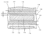
この方法においては、例えば、図28に示すように、複数のチップに分割されることになるマザー積層体を構成する複数のセラミックグリーンシート111,112上の帯状の電極不存在部分116に、内部電極113から所定の間隔aをおいて、内部電極113の長辺114と平行に延びる導電性のずれ検出パターン117を形成している。そして、このマザー積層体をカット線118に沿ってカットした場合、位置ずれがあって、得られるチップの外表面から内部電極113までの距離(ギャップ)が不十分な場合には、ずれ検出パターン117の少なくとも一部がチップ内に取り込まれ、この取り込まれたずれ検出パターン117が一対の外部電極間を短絡させる。したがって、外部電極間の抵抗を測定することにより、内部電極113の不適正状態を把握することが可能になる。
【0004】
【特許文献1】
特開平8−330178号公報
【0005】
【発明が解決しようとする課題】
しかしながら、上記特許文献1の方法では、図29に示すように、カット線118が、ずれ検出パターン117の長手方向に対して斜めに傾いた場合、ずれ検出パターン117が一対の外部電極間を短絡させなくなり、位置ずれを検出できないという問題点がある。
【0006】
また、特許文献1の方法では、同一のセラミックグリーンシート上に、内部電極パターンと、ずれ検出パターンの両方を印刷するため、シート面積あたりのチップの取り個数が少なくなるという問題点がある。
【0007】
また、シート面積あたりのチップの取り個数を増やすために、内部電極パターンと、ずれ検出パターンの距離を小さくすると、内部電極の周縁部とチップ端面との距離が小さくなるため、耐圧信頼性が低下するという問題点がある。
【0008】
本願発明は上記問題点を解決するものであり、マザー積層体の平面面積あたりのチップの取り個数を減らすことなく、内部電極パターンの位置ずれを確実に検出することが可能で、信頼性の高い積層セラミック電子部品及び、信頼性の高い積層セラミック電子部品を効率よく製造することが可能な積層セラミック電子部品の製造方法を提供することを目的とする。
【0009】
【課題を解決するための手段】
上記目的を達成するために、本願発明(請求項1)の積層セラミック電子部品の製造方法は、
(a)セラミックグリーンシートに所定の内部電極パターンが配設された内部電極パターン配設シートを形成する工程と、
(b)セラミックグリーンシートに、カットずれが起きた場合に外部電極と導通する位置ずれ検出パターンが配設された位置ずれ検出パターン配設シートを形成する工程と、
(c)前記内部電極パターン配設シートと、前記位置ずれ検出パターン配設シートを積層して未焼結マザー積層体を形成する工程と、
(d)前記未焼結マザー積層体をカットすることにより個々のチップ型未焼結積層体に分割する工程と、
(e)前記チップ型未焼結積層体を焼成することにより、内部電極を備えたセラミック焼結体を形成する工程と、
(f)前記セラミック焼結体の表面に所定の内部電極と接続する外部電極を形成する工程と、
(g)前記(f)の工程で外部電極を形成することにより得られる積層セラミック電子部品について電気特性を測定し、
(イ)前記内部電極パターン及び位置ずれ検出パターンに位置ずれが生じており、前記(c)の工程で未焼結マザー積層体をカットして個々のチップ型未焼結積層体に分割したときに、前記位置ずれ検出パターンがチップの切断端面に露出して、前記外部電極と導通している場合と、
(ロ)前記内部電極パターン及び位置ずれ検出パターンに位置ずれが生じておらず、前記(c)の工程で未焼結マザー積層体をカットして個々のチップ型未焼結積層体に分割したときに、前記位置ずれ検出パターンがチップ型未焼結積層体の切断端面に露出せず、前記外部電極と導通していない場合と
における電気特性の差異の大きさから前記電極パターンの位置ずれの有無を検出する工程と
を具備することを特徴としている。
【0010】
内部電極パターンが配設された内部電極パターン配設シートと、位置ずれ検出パターンが配設された位置ずれ検出パターン配設シートを形成し、この内部電極パターン配設シート及び位置ずれ検出パターン配設シートを積層して未焼結マザー積層体を形成し、未焼結マザー積層体をカットして個々のチップ型未焼結積層体に分割した後、焼成し、所定の内部電極と接続する外部電極を形成することにより得られる積層セラミック電子部品について電気特性を測定することにより、(イ)位置ずれが生じており、未焼結マザー積層体をカットして個々のチップ型未焼結積層体に分割したときに、位置ずれ検出パターンがチップの切断端面に露出して、外部電極と導通している場合と、(ロ)位置ずれが生じておらず、未焼結マザー積層体をカットして個々のチップ型未焼結積層体に分割したときに、位置ずれ検出パターンがチップ型未焼結積層体の切断端面に露出せず、外部電極と導通していない場合における電気特性の相違を検出し、かかる電気特性の差異の大きさから、電極パターンの位置ずれの有無を確実に検出することが可能になる。
すなわち、未焼結マザー積層体をカットして個々のチップ型未焼結積層体に分割した際に個々のチップ型未焼結積層体の切断端部となる周縁部より内側の領域に、所定の位置ずれ検出パターンを配設し、位置ずれが生じた場合に該位置ずれ検出パターンと外部電極が接続することによる電気特性の変化を検出することにより、位置ずれが生じた不良品を確実に検出して、位置ずれのない良品のみを確実に出荷できるようになる。
また、実際のカット線が、所定のカット線に対してある程度の傾きがあるような場合にも、内部電極パターンの位置ずれを検出して、信頼性の高い積層セラミック電子部品を効率よく製造することが可能になる。
【0011】
また、本願発明においては、マザー積層体を構成するマザーシートの同一平面に内部電極パターンと位置ずれ検出パターンの両方を形成する必要がないため、マザー積層体の平面面積あたりのチップ型未焼結積層体の取り個数を多くすることが可能になる。
【0012】
また、請求項2の積層セラミック電子部品の製造方法は、キャパシタ機能、インダクタ機能、及びインピーダンス機能のうちの少なくとも1つの機能を有する積層セラミック電子部品の製造方法にかかるものであることを特徴としている。
【0013】
本願発明は、キャパシタ機能、インダクタ機能、及びインピーダンス機能のうちの少なくとも1つの機能を有する積層セラミック電子部品を製造する場合に広く適用することが可能であり、このような積層セラミック電子部品の製造方法に本願発明を適用することにより、積層セラミックコンデンサ、積層セラミックインダクタ、及び積層セラミックフィルタのような積層LC複合部品などの積層セラミック電子部品を効率よく製造することが可能になる。
【0014】
また、請求項3の積層セラミック電子部品の製造方法は、前記電気特性として、キャパシタンス、インダクタンス、及びインピーダンスのうちの少なくとも1つを測定して電極パターンの位置ずれを検出することを特徴としている。
【0015】
本願発明においては、電気特性として、キャパシタンス、インダクタンス、及びインピーダンスのうちの少なくとも1つの電気特性を測定することにより、電極パターンの位置ずれの有無を容易かつ確実に検出することができる。
【0016】
また、本願発明(請求項4)の積層セラミック電子部品は、
内部電極パターンが配設された内部電極パターン配設シートと、カットずれが起きた場合に外部電極と導通する位置ずれ検出パターンが配設された位置ずれ検出パターン配設シートを積層することにより未焼結マザー積層体を形成し、これをカットすることにより得られるチップ型未焼結積層体を焼成して形成したセラミック焼結体の表面に、所定の内部電極と接続する外部電極が配設された積層セラミック電子部品であって、
キャパシタンス、インダクタンス、及びインピーダンスのうちの少なくとも1つを測定することによりカットずれの有無が検出されるように構成されていること
を特徴としている。
【0017】
本願発明の積層セラミック電子部品は、内部電極パターン配設シートと、カットずれが起きた場合に外部電極と導通する位置ずれ検出パターンが配設された位置ずれ検出パターン配設シートを積層して未焼結マザー積層体を形成し、これをカットすることにより得られるチップ型未焼結積層体を焼成したセラミック焼結体の表面に、所定の内部電極と接続する外部電極が配設された構成を備えているので、キャパシタンス、インダクタンス、及びインピーダンスのうちの少なくとも1つを測定することによりカットずれの有無を検出することが可能になり、信頼性の高い積層セラミック電子部品を確実に提供することが可能になる。
【0018】
【実施例】
以下、本願発明の実施例を示して、本願発明の特徴とするところをさらに詳しく説明する。
【0019】
[実施例1]
(1)ドクターブレードなどの方法により、TiO2−BaO系の誘電体セラミック層用スラリーをシート状に成形してセラミックグリーンシートを作製する。
それから、図1に示すように、セラミックグリーンシート(誘電体シート)1の表面に導電ペーストを印刷して、所定の内部電極パターン(コンデンサ用グランドパターン2a、及びホットパターン2b)が配設された内部電極パターン配設シート3a,3bを形成する。
また、同様にして、セラミックグリーンシート1の表面に導電ペーストを印刷して、後の工程で未焼結マザー積層体をカットして個々のチップ型未焼結積層体に分割した場合に、個々のチップ型未焼結積層体の切断端部となる周縁部の内側の領域に、所定の位置ずれ検出パターン4を印刷することにより、位置ずれ検出パターン配設シート5を形成する。
【0020】
(2)また、ドクターブレードなどの方法により、Fe2O3−NiO−ZnO−CuO系の磁性体セラミック層用スラリーをシート状に成形してセラミックグリーンシート(磁性体シート)6を作製する。
そして、このセラミックグリーンシート6に、ビアホール用貫通孔(図示せず)を形成するとともに、導電ペーストを印刷することにより、所定のコイルパターン(内部電極パターン)7が配設されたコイルパターン配設シート(内部電極パターン配設シート)8を形成する。
【0021】
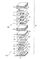
(3)そして、内部電極パターン配設シート3a,3b、位置ずれ検出パターン配設シート5、コイルパターン配設シート8、導体パターンが配設されていない誘電体シート1a及び磁性体シート6aを、図1に示すような所定の順に積み重ね、圧着した後、所定の寸法にカットし、チップ型未焼結積層体10を得る。 なお、実際には、マザー積層体を形成し、これを所定の位置でカットして個々のチップ(未焼結積層体)に分割して多数個のチップを同時に製造する、いわゆる多数個取りの方法が用いられる。図1はカットされた後のチップ型未焼結積層体の分解斜視図である。
なお、このチップ型未焼結積層体10は、コンデンサ用グランドパターン2a、及びホットパターン2bなどからなるコンデンサ部10aと、ビアホール(図示せず)を介して、コイルパターン(内部電極パターン)7を導通させることにより形成された積層型コイル9を有するコイル部10bを備えている。
【0022】
(4)それから、チップ型未焼結積層体10を、例えば、空気中、500℃で脱バインダ処理した後、900℃で約2時間、焼成処理を施すことにより、コンデンサ部10a,コイル部10bを備えたセラミック焼結体F(図1,図2,図3など)を形成する。
【0023】
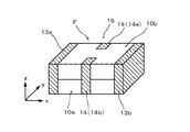
(5)次に、図2に示すように、セラミック焼結体Fの表面に、コイルパターン7、及びコンデンサ用ホットパターン2bと導通する外部電極(入出力端子)13a、13b、ならびにコンデンサ用グランドパターン2aと導通する外部電極(グランド端子)14(14a,14b)をそれぞれ形成し、図2に示すような積層セラミック電子部品(チップ型積層LCフィルタ)15を得る。
【0024】
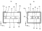
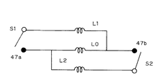
図3(a)は位置ずれの生じていない状態のチップ型積層LCフィルタ15の長手方向に沿う方向の断面図、図3(b)は位置ずれの生じていない状態のチップ型積層LCフィルタ15の長手方向に直交する方向の断面図である。
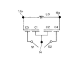
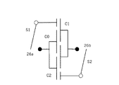
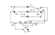
また、図4はこのチップ型積層LCフィルタ15の等価回路を示す図である。図4の等価回路において、S1、S2は位置ずれ検出パターン4と外部電極14により形成される、位置ずれを検出するためのスイッチである。
【0025】
次に、このチップ型積層LCフィルタにおいて、製造工程(カット工程)で未焼結マザー積層体をカットする際に位置ずれが生じた製品を検出する方法について説明する。
なお、図5はコンデンサ用ホットパターン2bの引き出し方向と直交する方向(y方向)に位置ずれが生じた状態のチップ型積層LCフィルタ15を示す断面図(長手方向に直交する方向の断面図)である。
【0026】
許容範囲を超えた位置ずれが生じた製品を検出するにあたっては、まず、
f≪(C1+C2)1/2/{2π(L0×C1×C2)1/2}
の周波数条件で、
(イ)外部電極13a−13b間のインダクタンス
(ロ)外部電極13a−14間のキャパシタンス
(ハ)外部電極13b−14間のキャパシタンス
を測定する。
【0027】
このとき、図3(a),(b)に示すように、位置ずれが生じていない状態から、図5に示すように、コンデンサ用ホットパターン2bの引き出し方向と直交する方向(y方向)に、許容範囲を超える位置ずれが発生した場合、位置ずれ検出パターン(位置ずれ検出電極)4が外部電極14(14a)と接触することにより、図4の等価回路において、スイッチS1,S2がONになり、外部電極13a・13b−14間で発生するキャパシタンスが変化する。
【0028】
すなわち、
(a)許容範囲を超える位置ずれがなく、スイッチS1、S2がOFFの場合の各部の特性は、
外部電極13a−13b間のインダクタンス=L0
外部電極13a−14間のキャパシタンス=C1+C2
外部電極13b−14間のキャパシタンス=C1+C2
となる。
(b)また、許容範囲を超える位置ずれがあり、位置ずれ検出パターン(位置ずれ検出電極)が外部電極14と接触し、スイッチS1、S2がONになった場合、各部の特性は、
外部電極13a−13b間のインダクタンス=L0
外部電極13a−14間のキャパシタンス=C1+C2+C3+C4
外部電極13b−14間のキャパシタンス=C1+C2+C3+C4
となる。
【0029】
したがって、上記実施例1の方法によれば、y方向への加工ずれが発生した場合、スイッチS1、S2がONとなり、キャパシタンスが変化するので、外部電極13a−14間,外部電極13b−14間のキャパシタンスを調べることによって、位置ずれが生じた製品を確実に検出することが可能になり、耐圧信頼性の低い製品を出荷することを防止して、長期間使用しても絶縁抵抗が劣化するおそれの少ない、信頼性の高い製品を確実に供給することが可能になる。
なお、積層セラミック電子部品は、通常、全数について主要特性を測定、選別した後出荷されるので、この測定、選別工程において、同時に位置ずれの発生した製品を検出することができるので、位置ずれ検出のために別途検査工程を設ける必要はなく、生産性を低下させることはない。
【0030】
なお、この実施例1では、図3(b)の符号Aで示す領域で絶縁抵抗が劣化しやすい態様で内部導体を設計したため、y方向の位置ずれを検出するようにしているが、絶縁抵抗が劣化しやすい領域は内部導体の設計にかかわるものであることから、内部導体の設計に応じて位置ずれ検出パターンの形状や配設態様を適宜調整することにより、効率よく位置ずれを検出することができる。
また、この実施例1では、2枚の位置ずれ検出パターン4を用いているが、位置ずれ検出パターンの枚数はこれに限られるものではなく、スイッチONにともなう電気特性の差異の検出が可能であればよく、1枚あるいは3枚以上とすることも可能である。
【0031】
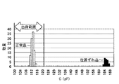
また、図6は所定の位置ずれ範囲内にあるチップ型積層LCフィルタと、意図的に許容範囲を超える位置ずれを生じさせたチップ型積層LCフィルタの端子導体13a−14間のキャパシタンスをヒストグラムでプロットしたものである。図6より、位置ずれが許容範囲を超えた場合に大きくキャパシタンスが変化し、出荷範囲をはずれることがわかる。
【0032】
[実施例2]
(1)ドクターブレードなどの方法により、TiO2−BaO系の誘電体セラミック層用スラリーをシート状に成形してセラミックグリーンシートを作製する。
それから、図7に示すように、セラミックグリーンシート(誘電体シート)21の表面に導電ペーストを印刷して、所定の内部電極パターン22a,22bが配設された内部電極パターン配設シート23a,23bを形成する。
また、同様にして、セラミックグリーンシート21の表面に導電ペーストを印刷して、後の工程で未焼結マザー積層体をカットして個々のチップ型未焼結積層体に分割した場合に、個々のチップの切断端部となる周縁部の内側の領域に、所定の位置ずれ検出パターン24を印刷することにより、位置ずれ検出パターン配設シート25を形成する。
【0033】
(2)そして、内部電極パターン配設シート23a,23b、位置ずれ検出パターン配設シート25、導体パターンが配設されていない誘電体シート21aを、図7に示すような所定の順に積み重ね、圧着した後、所定の寸法にカットし、チップ型未焼結積層体30を得る。図7はカットされた後のチップ型未焼結積層体30の分解斜視図である。
なお、実際には、マザー積層体を形成し、これを所定の位置でカットして個々のチップ型未焼結積層体に分割して多数個のチップを同時に製造する、いわゆる多数個取りの方法が用いられる。
【0034】
(3)それから、チップ型未焼結積層体30を、例えば、空気中、500℃で脱バインダ処理した後、900℃で約2時間、焼成処理を施すことにより、セラミック焼結体Fを形成する。
【0035】
(4)次に、図8に示すように、セラミック焼結体Fの表面にコンデンサ用の内部電極パターン22a,22b(図7)に導通する外部電極(入出力端子)26a、26bを形成し、図8に示すような積層セラミック電子部品(積層セラミックコンデンサ)27を得る。
【0036】
図9(a)は位置ずれの生じていない状態の積層セラミックコンデンサ27の長手方向に沿う方向の断面図、図9(b)は位置ずれの生じていない状態の積層セラミックコンデンサ27の長手方向に直交する方向の断面図である。
また、図10はこの積層セラミックコンデンサ27の等価回路を示す図である。図10の等価回路において、S1、S2は、位置ずれ検出パターン24と外部電極26a,26bにより形成される、位置ずれを検出するためのスイッチである。
【0037】
次に、この積層セラミックコンデンサにおいて、製造工程(カット工程)で未焼結マザー積層体をカットする際に位置ずれが生じた製品を検出する方法について説明する。
なお、図11は、内部電極パターン22a,22bに、その引き出し方向と平行な方向及び直交する方向の両方の方向に位置ずれが生じた状態の積層セラミックコンデンサ27を示す図であって、図11(a)は、長手方向に平行な方向の断面図、図11(b)は、長手方向に直交する方向の断面図である。
【0038】
許容範囲を超えた位置ずれの発生を検出するにあたっては、外部電極26a−26b間のキャパシタンスを測定する。
このとき、
(a)内部電極パターン22a,22bに許容範囲を超える位置ずれがなく、スイッチS1、S2がOFFの場合、
外部電極26a−26b間のキャパシタンス=C0
(b)スイッチS1がONの場合
26a−26b間のキャパシタンス=C0+C1
(c)スイッチS2がONの場合
26a−26b間のキャパシタンス=C0+C2
(d)スイッチS1、S2がONの場合
26a−26b間のキャパシタンス=C0+C1+C2
となる。
【0039】
したがって、上記実施例2の方法によれば、x方向への位置ずれが発生した場合、スイッチS1又はS2がONになり、y方向への位置ずれが発生した場合には、スイッチS1及びS2がONとなり、キャパシタンスが変化するので、外部電極26a−26b間のキャパシタンスを調べることによって、位置ずれが生じた製品を検出することが可能になり、耐圧信頼性の低い製品を出荷することを防止して、長期間使用しても絶縁抵抗が劣化するおそれの少ない、信頼性の高い製品を確実に供給することが可能になる。
【0040】
なお、この実施例では、図9(a)に符号Aで示す領域、及び図9(b)に符号Bで示す領域で絶縁抵抗が劣化しやすい態様で内部導体を設計したため、x,y方向の位置ずれを検出するようにしているが、絶縁抵抗が劣化しやすい領域は内部導体の設計にかかわるものであることから、内部導体の設計に応じて位置ずれ検出パターンの形状や配設態様を適宜調整することにより、効率よく位置ずれを検出することができる。
【0041】
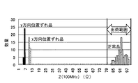
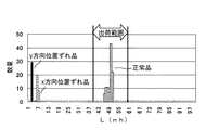
また、図12は所定の位置ずれ範囲内にある積層セラミックコンデンサと、意図的に許容範囲を超える位置ずれを生じさせた積層セラミックコンデンサの外部電極26a−26b間のキャパシタンスをヒストグラムでプロットしたものである。位置ずれが許容範囲を超えた場合に大きくキャパシタンスが変化し、出荷範囲をはずれることがわかる。
【0042】
[実施例3]
(1)ドクターブレードなどの方法により、Fe2O3−NiO−ZnO−CuO系の磁性体セラミック層用スラリーをシート状に成形してセラミックグリーンシート(磁性体シート)を作製する。
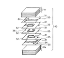
そして、図13に示すように、このセラミックグリーンシート31に、ビアホール用貫通孔(図示せず)を形成するとともに、導電ペーストを印刷して、所定のコイルパターン(内部電極パターン)32が配設されたコイルパターン配設シート33を形成する。
また、同様にして、セラミックグリーンシート31の表面に導電ペーストを印刷して、後の工程で未焼結マザー積層体をカットして個々のチップ型未焼結積層体に分割した場合に、個々のチップの切断端部となる周縁部の内側の領域に、所定の位置ずれ検出パターン34を印刷して、位置ずれ検出パターン配設シート35を形成する。
【0043】
(2)そして、コイルパターン配設シート33、位置ずれ検出パターン配設シート35、導体パターンが配設されていない磁性体シート31aを、図13に示すような順に積み重ね、圧着した後、所定の寸法にカットし、内部に積層型コイル36が形成されたチップ型未焼結積層体40を得る。
図13はカットされた後のチップ型未焼結積層体の分解斜視図である。
なお、実際には、マザー積層体を形成し、これを所定の位置でカットして個々のチップ型未焼結積層体に分割して多数個のチップを同時に製造する、いわゆる多数個取りの方法が用いられる。
【0044】
(3)それから、チップ型未焼結積層体40を、例えば、空気中、500℃で脱バインダ処理した後、900℃で約2時間、焼成処理を施すことにより、セラミック焼結体Fを形成する。
【0045】
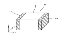
(4)次に、図14に示すように、セラミック焼結体Fの表面に、積層型コイル36の両端部を構成するコイルパターン32に導通した外部電極(入出力端子)37a、37bを形成し、図14に示すような積層セラミック電子部品(積層インダクタ)38を得る。 なお、この積層インダクタは、インピーダンスを主要な特性とするものであって、ビーズインダクタとも称される積層インダクタである。
【0046】
図15(a)は位置ずれの生じていない状態の積層インダクタ38の長手方向に沿う方向の断面図、図15(b)は位置ずれの生じていない状態の積層インダクタ38の長手方向に直交する方向の断面図である。
また、図16はこの積層インダクタ38の等価回路を示す図である。図16の等価回路において、S1、S2は位置ずれを検出するためのスイッチである。
【0047】
次に、この積層インダクタにおいて、製造工程(カット工程)で未焼結マザー積層体をカットする際に位置ずれが生じた製品を検出する方法について説明する。
なお、図17は、コイルパターン32に、その引き出し方向と平行な方向及び直交する方向の両方の方向に位置ずれが生じた状態の積層インダクタ38を示す図であって、図17(a)は長手方向に平行な方向の断面図、図17(b)は長手方向に直交する方向の断面図である。
【0048】
許容範囲を超えた位置ずれの発生を検出するにあたっては、外部電極37a−37b間のインピーダンスを測定する。
このとき、例えば、
(a)位置ずれが生じておらず、スイッチS1、S2がOFFの場合
外部電極37a−37b間のインピーダンス=Z0
(b)x方向に位置ずれが生じ、スイッチS1がONになった場合
外部電極37a−37b間のインピーダンス=Z0×Z1/(Z0+Z1)
(c)x方向に位置ずれが生じ、スイッチS2がONになった場合
外部電極37a−37b間のインピーダンス=Z0×Z2/(Z0+Z2)
(d)y方向に位置ずれが生じ、スイッチS1、S2がONになった場合
外部電極37a−37b間のインピーダンス
=Z0×Z1×Z2/{(Z0×Z1)+(Z1×Z2)+(Z2×Z0)}
となる。
【0049】
したがって、上記実施例3の方法によれば、x方向への位置ずれが発生した場合、スイッチS1又はS2がONとなり、y方向への位置ずれが発生した場合、スイッチS1及びS2がONとなり、インピーダンスが変化するので、外部電極37a−37b間のインピーダンスを調べることにより、位置ずれが生じた製品を検出することが可能になり、耐圧信頼性の低い製品を出荷することを防止して、長期間使用しても絶縁抵抗が劣化するおそれの少ない、信頼性の高い製品を確実に供給することが可能になる。
【0050】
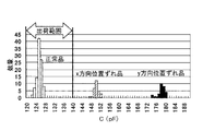
なお、この実施例では、図15(a)に符号Aで示す領域、及び図15(b)に符号Bで示す領域で絶縁抵抗が劣化しやすい態様で内部導体を設計したため、x,y方向の位置ずれを検出するようにしているが、絶縁抵抗が劣化しやすい領域は内部導体の設計にかかわるものであることから、内部導体の設計に応じて位置ずれ検出パターンの形状や配設態様を適宜調整することにより、効率よく位置ずれを検出することができる。なお、図15(a),(b)のA,Bで示す領域の絶縁抵抗が劣化した場合、インピーダンスの低下を招く。
【0051】
また、図18は所定の位置ずれ範囲内にある積層インダクタと、意図的に許容範囲を超える位置ずれを生じさせた積層インダクタの外部電極37a−37b間のインピーダンスをヒストグラムでプロットしたものである。位置ずれが許容範囲を超えた場合に大きくインピーダンスが変化し、出荷範囲をはずれることがわかる。
【0052】
[実施例4]
(1)ドクターブレードなどの方法により、ホウケイ酸ガラスと、Al2O3とからなるガラスセラミックスラリーをシート状に成形してセラミックグリーンシート(磁性体シート)を作製する。
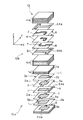
そして、図19に示すように、このセラミックグリーンシート41に、ビアホール用貫通孔(図示せず)を形成するとともに、導電ペーストを印刷することにより、所定のコイルパターン(内部電極パターン)42が配設されたコイルパターン配設シート43を形成する。
また、同様にして、セラミックグリーンシート41の表面に導電ペーストを印刷することにより、後の工程で未焼結マザー積層体をカットして個々のチップ型未焼結積層体に分割した場合に、個々のチップの切断端部となる周縁部の内側の領域に、所定の位置ずれ検出パターン44を印刷することにより、位置ずれ検出パターン配設シート45を形成する。
【0053】
(2)そして、コイルパターン配設シート43、位置ずれ検出パターン配設シート45、導体パターンが配設されていない磁性体シート41aを、図19に示すような所定の順に積み重ね、これを一括して圧着した後、所定の寸法にカットし、内部に積層型コイル46が形成されたチップ型未焼結積層体50を得る。図19はカットされた後のチップ型未焼結積層体の分解斜視図である。
なお、実際には、マザー積層体を形成し、これを所定の位置でカットして個々のチップ型未焼結積層体に分割して多数個のチップを同時に製造する、いわゆる多数個取りの方法が用いられる。
【0054】
(3)それから、チップ型未焼結積層体50を、例えば、空気中、500℃で脱バインダ処理した後、900℃で約2時間、焼成処理を施すことにより、セラミック焼結体Fを形成する。
【0055】
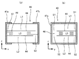
(4)次に、図20に示すように、セラミック焼結体Fの表面に、積層型コイル46の両端部を構成するコイルパターン42に導通した外部電極(入出力端子)47a、47bを形成し、図20に示すような積層セラミック電子部品(積層インダクタ)48を得る。
【0056】
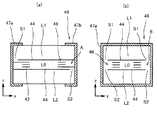
図21(a)は位置ずれの生じていない状態の積層インダクタ48の長手方向に沿う方向の断面図、図21(b)は位置ずれの生じていない状態の積層インダクタ48の長手方向に直交する方向の断面図である。
また、図22はこの積層インダクタ48の等価回路を示す図である。図22の等価回路において、S1、S2は位置ずれを検出するためのスイッチである。
なお、この積層インダクタは、インダクタンスを主要な特性とする積層インダクタである。
【0057】
次に、この積層インダクタにおいて、製造工程(カット工程)で未焼結マザー積層体をカットする際に位置ずれが生じた製品を検出する方法について説明する。
なお、図23は、コイルパターン42に、その引き出し方向と平行な方向及び引き出し方向と直交する方向の両方の方向に位置ずれが生じた状態の積層インダクタ48を示す図であって、図23(a)は長手方向に平行な方向の断面図、図23(b)は長手方向に直交する方向の断面図である。
【0058】
許容範囲を超えた位置ずれの発生を検出するにあたっては、外部電極47a−47b間のインダクタンスを測定する。
このとき、
(a)位置ずれが生じておらず、スイッチS1、S2がOFFの場合
外部電極47a−47b間のインダクタンス=L0
(b)x方向に位置ずれが生じ、スイッチS1がONになった場合
外部電極47a−47b間のインダクタンス=L0×L1/(L0+L1)
(c)x方向に位置ずれが生じ、スイッチS2がONになった場合
外部電極47a−47b間のインダクタンス=L0×L2/(L0+L2)
(d)y方向に位置ずれが生じ、スイッチS1、S2がONになった場合
外部電極47a−47b間のインダクタンス
=L0×L1×L2/{(L0×L1)+(L1×L2)+(L2×L0)}
となる。
【0059】
したがって、上記実施例4の方法によれば、x方向への位置ずれが発生した場合、スイッチS1又はS2がONとなり、y方向への位置ずれが発生した場合、スイッチS1及びS2がONとなり、インダクタンスが変化するので、外部電極47a−47b間のインダクタンスを調べることにより、位置ずれが生じた製品を検出することが可能になり、信頼性の高い製品を確実に供給することが可能になる。
【0060】
なお、この実施例4では、図21(a)に符号Aで示す領域、及び図21(b)に符号Bで示す領域で絶縁抵抗が劣化しやすい態様で内部導体を設計したため、x,y方向の位置ずれを検出するようにしたが、絶縁抵抗が劣化しやすい領域は内部導体の設計にかかわるものであることから、内部導体の設計に応じて位置ずれ検出パターンの形状や配設態様を適宜調整することにより、効率よく位置ずれを検出することができる。
【0061】
また、図24は所定の位置ずれ範囲内にある積層インダクタと、意図的に許容範囲を超える位置ずれを生じさせた積層インダクタの外部電極47a−47b間のインダクタンスをヒストグラムでプロットしたものである。位置ずれが許容範囲を超えた場合に大きくインダクタンスが変化し、出荷範囲をはずれることがわかる。
【0062】
[実施例5]
図25は本願発明の他の実施例(実施例5)にかかる積層セラミック電子部品の要部を示す分解斜視図、図26は断面図、図27は等価回路を示す図である。
この実施例5の積層セラミック電子部品は、3端子積層型LCローパスフィルタであり、この3端子積層型LCローパスフィルタは、上述の実施例1のチップ型積層LCフィルタに類似した構造を有しており、
(a)コンデンサ部10aに、グランドパターン2aの位置ずれ(y方向の位置ずれ)を検出するための位置ずれ検出パターン54aと、ホットパターン2bの位置ずれ(x方向の位置ずれ)を検出するための位置ずれ検出パターン54bが配設されている点、
(b)コイル部10bにも位置ずれ検出パターン64a,64bが配設されている点
においてその構成が実施例1とは異なっているが、その他の構成は実施例1の場合とほぼ同様である。したがって、重複を避けるため、ここでは実施例1と同じ構成の部分については説明を省略する。なお、図25,26,27において、図1,2,3,4と同一符号を付した部分は同一部分又は相当する部分を示している。
【0063】
この実施例5の3端子積層型LCローパスフィルタにおいては、許容範囲を超える位置ずれがなく、スイッチS1、S2,S3,S4がOFFの場合の各部の特性は、
外部電極13a−13b間のインダクタンス=L0
外部電極13a−14間のキャパシタンス=C1+C2
外部電極13b−14間のキャパシタンス=C1+C2
となる。
【0064】
また、許容範囲を超える位置ずれがあり、例えば、スイッチS1,S2,S3,S4がONになった場合、
外部電極13a−13b間のインダクタンス
=L0×L1×L2/{(L0×L1)+(L1×L2)+(L2×L0)}
となり、
外部電極13a−14間のキャパシタンス=C1+C2+C3+C4
外部電極13b−14間のキャパシタンス=C1+C2+C3+C4
となる。
【0065】
したがって、外部電極13a−13b間のインダクタンス、外部電極13a・13b−14間のキャパシタンスを調べることにより、位置ずれが生じた製品を検出することが可能になり、耐圧信頼性の低い製品が出荷されてしまうことを防止して、信頼性の高い製品を確実に供給することが可能になる。
【0066】
なお、本願発明は、上記の各実施例に限定されるものではなく、内部電極パターン及び位置ずれ検出パターンの具体的な形状や配設態様、位置ずれを検出するために測定すべき特性、その具体的な測定方法などに関し、発明の範囲内において、種々の応用、変形を加えることが可能である。
【0067】
【発明の効果】
上述のように、本願発明(請求項1)の積層セラミック電子部品の製造方法は、内部電極パターンが配設された内部電極パターン配設シートと、位置ずれ検出パターンが配設された位置ずれ検出パターン配設シートを形成し、この内部電極パターン配設シート及び位置ずれ検出パターン配設シートを積層して未焼結マザー積層体を形成し、未焼結マザー積層体をカットして個々のチップ型未焼結積層体に分割した後、焼成し、所定の内部電極と接続する外部電極を形成することにより得られる積層セラミック電子部品について電気特性を測定するようにしてるので、(イ)位置ずれが生じており、未焼結マザー積層体をカットして個々のチップ型未焼結積層体に分割したときに、位置ずれ検出パターンがチップ型未焼結積層体の切断端面に露出して、外部電極と導通している場合と、(ロ)位置ずれが生じておらず、未焼結マザー積層体をカットして個々のチップ型未焼結積層体に分割したときに、位置ずれ検出パターンがチップ型未焼結積層体の切断端面に露出せず、外部電極と導通していない場合における電気特性の相違を検出し、かかる電気特性の差異の大きさから、電極パターンの位置ずれの有無を確実に検出することが可能になる。
すなわち、未焼結マザー積層体をカットして個々のチップ型未焼結積層体に分割した際に個々のチップ型未焼結積層体の切断端部となる周縁部より内側の領域に、所定の位置ずれ検出パターンを配設し、位置ずれが生じた場合に該位置ずれ検出パターンと外部電極が接続することによる電気特性の変化を検出することにより、位置ずれが生じた不良品を確実に検出することができるようになる。
また、実際のカット線が、所定のカット線に対してある程度の傾きがあるような場合にも、内部電極パターンの位置ずれを確実に検出することが可能になる。
さらに、本願発明においては、マザー積層体を構成するマザーシートの同一平面に内部電極パターンと位置ずれ検出パターンの両方を形成する必要がないため、マザー積層体の平面面積あたりのチップ型未焼結積層体の取り個数が少なくなることを防止することができる。
【0068】
また、請求項2の積層セラミック電子部品の製造方法のように、本願発明は、キャパシタ機能、インダクタ機能、及びインピーダンス機能のうちの少なくとも1つの機能を有する積層セラミック電子部品の製造方法に適用することが可能であり、このような積層セラミック電子部品の製造方法に本願発明を適用することにより、積層セラミックコンデンサ、積層セラミックインダクタ、及び積層セラミックフィルタのような積層LC複合部品などの積層セラミック電子部品を効率よく製造することができる。
【0069】
また、請求項3の積層セラミック電子部品の製造方法のように、電気特性として、キャパシタンス、インダクタンス、及びインピーダンスのうちの少なくとも1つの電気特性を測定することにより、電極パターンの位置ずれの有無を容易かつ確実に検出することが可能になり、本願発明をより実効あらしめることが可能になる。
【0070】
また、本願発明(請求項4)の積層セラミック電子部品は、内部電極パターン配設シートと、カットずれが起きた場合に外部電極と導通する位置ずれ検出パターンが配設された位置ずれ検出パターン配設シートを積層して未焼結マザー積層体を形成し、これをカットすることにより得られるチップ型未焼結積層体を焼成したセラミック焼結体の表面に、所定の内部電極と接続する外部電極が配設された構成を備えているので、キャパシタンス、インダクタンス、及びインピーダンスのうちの少なくとも1つを測定することによりカットずれの有無を検出することが可能になり、信頼性の高い積層セラミック電子部品を確実に提供することが可能になる。
【図面の簡単な説明】
【図1】本願発明の一実施例(実施例1)にかかる積層セラミック電子部品(チップ型積層LCフィルタ)の製造方法の一工程で形成したチップ型未焼結積層体の分解斜視図である。
【図2】実施例1において製造したチップ型積層LCフィルタを示す斜視図である。
【図3】実施例1において製造した、位置ずれの生じていない状態のチップ型積層LCフィルタの断面図であり、(a)はチップ型積層LCフィルタ15の長手方向に沿う方向の断面図、(b)は長手方向に直交する方向の断面図である。
【図4】実施例1において製造したチップ型積層LCフィルタの等価回路を示す図である。
【図5】実施例1において製造したチップ型積層LCフィルタにおいて位置ずれが生じた状態を示す、長手方向に直交する方向の断面図である。
【図6】実施例1において製造したチップ型積層LCフィルタの、位置ずれが生じたものと、位置ずれが生じていないもののキャパシタンスのヒストグラムを示す図である。
【図7】本願発明の他の実施例(実施例2)にかかる積層セラミック電子部品(積層セラミックコンデンサ)の製造方法の一工程で形成したチップ型未焼結積層体の分解斜視図である。
【図8】実施例2において製造した積層セラミックコンデンサを示す斜視図である。
【図9】実施例2において製造した、位置ずれの生じていない積層セラミックコンデンサの断面図であり、(a)は積層セラミックコンデンサの長手方向に沿う方向の断面図、(b)は長手方向に直交する方向の断面図である。
【図10】実施例2において製造した積層セラミックコンデンサの等価回路を示す図である。
【図11】実施例2において製造した積層セラミックコンデンサにおいて位置ずれが生じた状態を示す断面図であり、(a)は積層セラミックコンデンサの長手方向に沿う方向の断面図、(b)は長手方向に直交する方向の断面図である。
【図12】実施例2において製造したチップ型積層LCフィルタの、位置ずれが生じたものと、位置ずれが生じていないもののキャパシタンスのヒストグラムを示す図である。
【図13】本願発明のさらに他の実施例(実施例3)にかかる積層セラミック電子部品(積層インダクタ)の製造方法の一工程で形成したチップ型未焼結積層体の分解斜視図である。
【図14】実施例3において製造した積層インダクタを示す斜視図である。
【図15】実施例3において製造した、位置ずれの生じていない積層インダクタの断面図であり、(a)は積層インダクタの長手方向に沿う方向の断面図、(b)は長手方向に直交する方向の断面図である。
【図16】実施例3において製造した積層セラミックコンデンサの等価回路を示す図である。
【図17】実施例3において製造した積層インダクタにおいて位置ずれが生じた状態を示す断面図であり、(a)は積層インダクタの長手方向に沿う方向の断面図、(b)は長手方向に直交する方向の断面図である。
【図18】実施例3において製造した積層インダクタの、位置ずれが生じたものと、位置ずれが生じていないもののインピーダンスのヒストグラムを示す図である。
【図19】本願発明のさらに他の実施例(実施例4)にかかる積層セラミック電子部品(積層インダクタ)の製造方法の一工程で形成したチップ型未焼結積層体の分解斜視図である。
【図20】実施例4において製造した積層インダクタを示す斜視図である。
【図21】実施例4において製造した、位置ずれの生じていない積層インダクタの断面図であり、(a)は積層インダクタの長手方向に沿う方向の断面図、(b)は長手方向に直交する方向の断面図である。
【図22】実施例4において製造した積層インダクタの等価回路を示す図である。
【図23】実施例4において製造した積層インダクタにおいて位置ずれが生じた状態を示す断面図であり、(a)は積層インダクタの長手方向に沿う方向の断面図、(b)は長手方向に直交する方向の断面図である。
【図24】実施例4において製造した積層インダクタの、位置ずれが生じたものと、位置ずれが生じていないもののインダクタンスのヒストグラムを示す図である。
【図25】本願発明のさらに他の実施例(実施例5)にかかる積層セラミック電子部品(3端子積層型LCローパスフィルタ)の要部を示す分解斜視図である。
【図26】実施例5の3端子積層型LCローパスフィルタの長手方向に沿う方向の断面図である。
【図27】実施例5の3端子積層型LCローパスフィルタの等価回路を示す図である。
【図28】従来の積層セラミック電子部品の製造方法の一工程を示す図である。
【図29】従来の積層セラミック電子部品の製造方法の問題点を説明する図である。
【符号の説明】
1 セラミックグリーンシート(誘電体シート)
1a 導体パターンが配設されていない誘電体シート
2a 内部電極パターン(コンデンサ用のグランドパターン)
2b 内部電極パターン(コンデンサ用のホットパターン)
3a,3b 内部電極パターン配設シート
4 位置ずれ検出パターン
5 位置ずれ検出パターン配設シート
6 セラミックグリーンシート
6a 磁性体シート
7 コイルパターン(内部電極パターン)
8 コイルパターン配設シート
9 積層型コイル
10 チップ型未焼結積層体
10a コンデンサ部
10b コイル部
13a、13b 外部電極(入出力端子)
14(14a,14b) 外部電極(グランド端子)
15 積層セラミック電子部品(チップ型積層LCフィルタ)
21 セラミックグリーンシート(誘電体シート)
21a 導体パターンが配設されていない誘電体シート
22a,22b 内部電極パターン
23a,23b 内部電極パターン配設シート
24 位置ずれ検出パターン
25 位置ずれ検出パターン配設シート
26a、26b 外部電極(入出力端子)
27 積層セラミック電子部品(積層セラミックコンデンサ)
30 チップ型未焼結積層体
31 セラミックグリーンシート
31a 導体パターンが配設されていない磁性体シート
32 コイルパターン(内部電極パターン)
33 コイルパターン配設シート
34 位置ずれ検出パターン
35 位置ずれ検出パターン配設シート
36 積層型コイル
37a、37b 外部電極(入出力端子)
38 積層セラミック電子部品(積層インダクタ)
40 チップ型未焼結積層体
41 セラミックグリーンシート
41a 導体パターンが配設されていない磁性体シート
42 コイルパターン(内部電極)
43 コイルパターン配設シート
44 位置ずれ検出パターン
45 位置ずれ検出パターン配設シート
46 積層型コイル
47a、47b 外部電極(入出力端子)
48 積層セラミック電子部品(積層インダクタ)
50 チップ型未焼結積層体
54a グランドパターンの位置ずれ検出パターン
54b ホットパターンの位置ずれ検出パターン
64a,64b コイル部の位置ずれ検出パターン
F セラミック焼結体
S1,S2,S3,S4 位置ずれを検出するためのスイッチ
C0,C1,C2,C3,C4 キャパシタンス
Z0,Z1,Z2 インピーダンス
L0,L1,L2 インダクタンス[0001]
TECHNICAL FIELD OF THE INVENTION
The present invention relates to a multilayer ceramic electronic component and a method for manufacturing the same, and more particularly, to a multilayer ceramic electronic component requiring high reliability and a method for manufacturing the same.
[0002]
[Prior art]
In the case of manufacturing a multilayer ceramic electronic component having an electrode (internal electrode) inside a chip, one of the methods for electrically detecting the displacement of the internal electrode is as follows, as described below. There is a method in which a conductive displacement detection pattern is provided inside to detect a displacement of an internal electrode (for example, see Patent Document 1).
[0003]
In this method, for example, as shown in FIG. 28, a plurality of ceramic
[0004]
[Patent Document 1]
JP-A-8-330178
[0005]
[Problems to be solved by the invention]
However, in the method of
[0006]
Further, in the method of
[0007]
In addition, if the distance between the internal electrode pattern and the misalignment detection pattern is reduced to increase the number of chips to be taken per sheet area, the distance between the peripheral portion of the internal electrode and the end face of the chip is reduced, thereby lowering the withstand voltage reliability. There is a problem that.
[0008]
The present invention solves the above-described problems, and it is possible to reliably detect the displacement of the internal electrode pattern without reducing the number of chips to be taken per plane area of the mother laminate, and to achieve high reliability. It is an object of the present invention to provide a multilayer ceramic electronic component and a method of manufacturing a multilayer ceramic electronic component capable of efficiently manufacturing a highly reliable multilayer ceramic electronic component.
[0009]
[Means for Solving the Problems]
In order to achieve the above object, a method for manufacturing a multilayer ceramic electronic component according to the present invention (claim 1) includes:
(A) forming an internal electrode pattern arranging sheet in which a predetermined internal electrode pattern is arranged on a ceramic green sheet;
(B) forming, on the ceramic green sheet, a sheet having a misregistration detection pattern provided with a misregistration detection pattern that is electrically connected to the external electrode when a misalignment occurs;
(C) laminating the internal electrode pattern provision sheet and the misalignment detection pattern provision sheet to form an unsintered mother laminate;
(D) dividing the green mother laminate into individual chip-type green laminates by cutting;
(E) forming a ceramic sintered body having internal electrodes by firing the chip-type green laminate;
(F) forming an external electrode connected to a predetermined internal electrode on the surface of the ceramic sintered body;
(G) measuring the electrical characteristics of the multilayer ceramic electronic component obtained by forming the external electrodes in the step (f),
(A) When the internal electrode pattern and the positional shift detection pattern are misaligned, and the unsintered mother laminate is cut into individual chip-type unsintered laminates in the step (c). In the case where the misregistration detection pattern is exposed on the cut end surface of the chip and is electrically connected to the external electrodes,
(B) No misalignment occurs in the internal electrode pattern and misalignment detection pattern, and the unsintered mother laminate was cut and divided into individual chip-type unsintered laminates in the step (c). Sometimes, the misregistration detection pattern is not exposed to the cut end surface of the chip-type unsintered laminate, and is not electrically connected to the external electrode.
Detecting the presence or absence of a displacement of the electrode pattern from the magnitude of the difference in electrical characteristics in
It is characterized by having.
[0010]
Forming an internal electrode pattern disposition sheet on which the internal electrode pattern is disposed, and a displacement detection pattern disposition sheet on which the displacement detection pattern is disposed; and disposing the internal electrode pattern disposition sheet and the displacement detection pattern Sheets are laminated to form an unsintered mother laminate, and the unsintered mother laminate is cut and divided into individual chip-type unsintered laminates, which are then fired and connected to predetermined internal electrodes for external connection. By measuring the electrical properties of the multilayer ceramic electronic component obtained by forming the electrodes, (a) misalignment has occurred, and the unsintered mother laminate is cut into individual chip-type unsintered laminates. When the chip is divided into two parts, the misalignment detection pattern is exposed on the cut end surface of the chip and is electrically connected to the external electrodes. When the individual chip-type green laminates are divided into pieces, the misregistration detection pattern is not exposed on the cut end surface of the chip-type green laminate, and the difference in the electrical characteristics in a case where the pattern is not electrically connected to the external electrodes. And it is possible to reliably detect the presence / absence of a positional shift of the electrode pattern from the magnitude of the difference in the electrical characteristics.
That is, when the unsintered mother laminate is cut and divided into individual chip-type unsintered laminates, a predetermined area is provided in a region inside a peripheral edge that is a cut end of each chip-type unsintered laminate. By disposing the misregistration detection pattern and detecting a change in the electrical characteristics due to the connection between the misregistration detection pattern and the external electrode when the misregistration occurs, the defective product having the misregistration can be reliably detected. It is possible to reliably detect and ship only non-defective products with no misalignment.
In addition, even when the actual cut line has a certain degree of inclination with respect to the predetermined cut line, the displacement of the internal electrode pattern is detected to efficiently manufacture a highly reliable multilayer ceramic electronic component. It becomes possible.
[0011]
In addition, in the present invention, since it is not necessary to form both the internal electrode pattern and the misregistration detection pattern on the same plane of the mother sheet constituting the mother laminate, the chip-type unsintered surface area per plane area of the mother laminate is not required. It is possible to increase the number of stacked bodies.
[0012]
A second aspect of the present invention is directed to a method for manufacturing a multilayer ceramic electronic component having at least one of a capacitor function, an inductor function, and an impedance function. .
[0013]
INDUSTRIAL APPLICABILITY The present invention can be widely applied to a case where a multilayer ceramic electronic component having at least one of a capacitor function, an inductor function, and an impedance function is manufactured, and a method for manufacturing such a multilayer ceramic electronic component. By applying the present invention, it is possible to efficiently manufacture a multilayer ceramic electronic component such as a multilayer LC composite component such as a multilayer ceramic capacitor, a multilayer ceramic inductor, and a multilayer ceramic filter.
[0014]
According to a third aspect of the invention, there is provided a method for manufacturing a multilayer ceramic electronic component, wherein at least one of capacitance, inductance, and impedance is measured as the electrical characteristic to detect a displacement of an electrode pattern.
[0015]
In the present invention, it is possible to easily and surely detect the presence / absence of the displacement of the electrode pattern by measuring at least one of the capacitance, the inductance, and the impedance as the electric characteristics.
[0016]
Further, the multilayer ceramic electronic component of the present invention (claim 4)
It is not possible to stack the internal electrode pattern placement sheet on which the internal electrode patterns are placed and the position shift detection pattern placement sheet on which the position shift detection patterns that are electrically connected to the external electrodes when a cut shift occurs. An external electrode connected to a predetermined internal electrode is provided on the surface of a ceramic sintered body formed by firing a chip-type unsintered laminate obtained by forming a sintered mother laminate and cutting it. A multilayer ceramic electronic component,
It is configured to detect the presence or absence of cut deviation by measuring at least one of capacitance, inductance, and impedance.
It is characterized by.
[0017]
The multilayer ceramic electronic component of the present invention is formed by laminating an internal electrode pattern arranging sheet and a misregistration detection pattern arranging sheet provided with a misalignment detection pattern which is electrically connected to an external electrode when a cut misalignment occurs. A structure in which external electrodes for connecting to predetermined internal electrodes are provided on the surface of a ceramic sintered body obtained by forming a sintered mother laminate and cutting the chip-type unsintered laminate obtained by cutting the same. Therefore, it is possible to detect the presence or absence of a cut shift by measuring at least one of capacitance, inductance, and impedance, and to reliably provide a highly reliable multilayer ceramic electronic component. Becomes possible.
[0018]
【Example】
Hereinafter, features of the present invention will be described in more detail by showing embodiments of the present invention.
[0019]
[Example 1]
(1) TiO is prepared by a method such as doctor blade. 2 -Form a ceramic green sheet by molding the BaO-based slurry for a dielectric ceramic layer into a sheet.
Then, as shown in FIG. 1, a conductive paste was printed on the surface of the ceramic green sheet (dielectric sheet) 1, and predetermined internal electrode patterns (
Similarly, when a conductive paste is printed on the surface of the ceramic
[0020]
(2) Also, by using a method such as a doctor blade, Fe 2 O 3 A ceramic green sheet (magnetic sheet) 6 is formed by forming a slurry for a magnetic ceramic layer based on —NiO—ZnO—CuO system into a sheet shape.
Then, a through-hole for a via hole (not shown) is formed in the ceramic
[0021]
(3) Then, the internal electrode
In addition, the chip-
[0022]
(4) Then, the chip
[0023]
(5) Next, as shown in FIG. 2, on the surface of the ceramic sintered body F, external electrodes (input / output terminals) 13a and 13b electrically connected to the
[0024]
FIG. 3A is a cross-sectional view in a direction along the longitudinal direction of the chip-type
FIG. 4 is a diagram showing an equivalent circuit of the chip-type
[0025]
Next, a description will be given of a method of detecting a product in which misalignment has occurred when the unsintered mother laminate is cut in the manufacturing process (cutting process) in the chip-type laminated LC filter.
FIG. 5 is a cross-sectional view (a cross-sectional view in a direction perpendicular to the longitudinal direction) showing the chip-type
[0026]
When detecting a product with a misalignment that exceeds the allowable range,
f≪ (C1 + C2) 1/2 / {2π (L0 × C1 × C2) 1/2 }
With the frequency condition of
(A) Inductance between the
(B) Capacitance between
(C) Capacitance between
Is measured.
[0027]
At this time, as shown in FIGS. 3 (a) and 3 (b), from a state in which no positional displacement occurs, as shown in FIG. 5, in a direction (y direction) orthogonal to the drawing direction of the capacitor
[0028]
That is,
(A) When there is no displacement exceeding the allowable range and the switches S1 and S2 are OFF, the characteristics of each part are as follows:
Inductance between
Capacitance between
Capacitance between
It becomes.
(B) Also, when there is a position shift exceeding the allowable range, the position shift detection pattern (position shift detection electrode) comes into contact with the
Inductance between
Capacitance between
Capacitance between
It becomes.
[0029]
Therefore, according to the method of the first embodiment, when a processing shift in the y direction occurs, the switches S1 and S2 are turned on, and the capacitance changes, so that the distance between the
In general, multilayer ceramic electronic components are shipped after measuring and sorting out the main characteristics of all the components. In this measurement and sorting process, products with misalignment can be detected at the same time. Therefore, there is no need to provide a separate inspection step, and the productivity is not reduced.
[0030]
In the first embodiment, since the inner conductor is designed in such a manner that the insulation resistance is easily deteriorated in a region indicated by the symbol A in FIG. 3B, the displacement in the y direction is detected. Since the area where is likely to deteriorate is related to the design of the internal conductor, the position deviation can be detected efficiently by appropriately adjusting the shape and arrangement of the position detection pattern according to the design of the internal conductor. Can be.
In the first embodiment, two
[0031]
FIG. 6 is a histogram showing the capacitance between the chip-type laminated LC filter within a predetermined positional deviation range and the
[0032]
[Example 2]
(1) TiO is prepared by a method such as doctor blade. 2 -Form a ceramic green sheet by molding the BaO-based slurry for a dielectric ceramic layer into a sheet.
Then, as shown in FIG. 7, a conductive paste is printed on the surface of the ceramic green sheet (dielectric sheet) 21 to form internal electrode
Similarly, when a conductive paste is printed on the surface of the ceramic
[0033]
(2) Then, the internal electrode
In practice, a so-called multi-cavity method in which a mother laminate is formed, cut at a predetermined position, divided into individual chip-type unsintered laminates, and a large number of chips are simultaneously manufactured. Is used.
[0034]
(3) After that, the chip-shaped
[0035]
(4) Next, as shown in FIG. 8, external electrodes (input / output terminals) 26a and 26b that are electrically connected to the
[0036]
FIG. 9A is a cross-sectional view in a direction along the longitudinal direction of the multilayer
FIG. 10 is a diagram showing an equivalent circuit of the multilayer
[0037]
Next, a description will be given of a method of detecting a product in which displacement has occurred when the unsintered mother laminate is cut in the manufacturing process (cutting process) in the multilayer ceramic capacitor.
FIG. 11 is a view showing the multilayer
[0038]
To detect the occurrence of a position shift exceeding the allowable range, the capacitance between the
At this time,
(A) When the
Capacitance between
(B) When switch S1 is ON
Capacitance between 26a-26b = C0 + C1
(C) When switch S2 is ON
Capacitance between 26a-26b = C0 + C2
(D) When switches S1 and S2 are ON
Capacitance between 26a-26b = C0 + C1 + C2
It becomes.
[0039]
Therefore, according to the method of the second embodiment, when the position shift in the x direction occurs, the switch S1 or S2 is turned on, and when the position shift in the y direction occurs, the switches S1 and S2 are turned off. ON, and the capacitance changes. By examining the capacitance between the
[0040]
In this embodiment, since the inner conductor is designed in such a manner that the insulation resistance is easily deteriorated in the region indicated by reference numeral A in FIG. 9A and the region indicated by reference numeral B in FIG. However, since the area where insulation resistance is likely to deteriorate is related to the design of the inner conductor, the shape and arrangement of the misalignment detection pattern should be adjusted according to the design of the inner conductor. By appropriately adjusting the position, the displacement can be detected efficiently.
[0041]
FIG. 12 is a graph in which the capacitance between the multilayer ceramic capacitor within a predetermined positional shift range and the
[0042]
[Example 3]
(1) Using a method such as a doctor blade, Fe 2 O 3 A ceramic green sheet (magnetic sheet) is formed by molding a slurry for a magnetic ceramic layer based on -NiO-ZnO-CuO system into a sheet shape.
Then, as shown in FIG. 13, through holes (not shown) for via holes are formed in the ceramic
Similarly, when a conductive paste is printed on the surface of the ceramic
[0043]
(2) Then, the coil
FIG. 13 is an exploded perspective view of the chip type green laminate after being cut.
In practice, a so-called multi-cavity method in which a mother laminate is formed, cut at a predetermined position, divided into individual chip-type unsintered laminates, and a large number of chips are simultaneously manufactured. Is used.
[0044]
(3) Then, the chip-shaped green
[0045]
(4) Next, as shown in FIG. 14, on the surface of the ceramic sintered body F, external electrodes (input / output terminals) 37a and 37b that are electrically connected to the
[0046]
FIG. 15A is a cross-sectional view in a direction along the longitudinal direction of the
FIG. 16 is a diagram showing an equivalent circuit of the
[0047]
Next, a description will be given of a method of detecting a product in which a displacement has occurred when the unsintered mother laminate is cut in the manufacturing process (cutting process) in the laminated inductor.
FIG. 17 is a diagram showing the
[0048]
In detecting the occurrence of a displacement exceeding the allowable range, the impedance between the
At this time, for example,
(A) When no displacement has occurred and switches S1 and S2 are OFF
Impedance between
(B) When a displacement occurs in the x direction and the switch S1 is turned on
Impedance between
(C) When a displacement occurs in the x direction and the switch S2 is turned on
Impedance between
(D) When displacement occurs in the y direction and switches S1 and S2 are turned on
Impedance between
= Z0 × Z1 × Z2 / {(Z0 × Z1) + (Z1 × Z2) + (Z2 × Z0)}
It becomes.
[0049]
Therefore, according to the method of the third embodiment, when the displacement in the x direction occurs, the switch S1 or S2 is turned on, and when the displacement in the y direction occurs, the switches S1 and S2 are turned on, Since the impedance changes, it is possible to detect a product in which a displacement has occurred by checking the impedance between the
[0050]
In this embodiment, since the inner conductor is designed in such a manner that the insulation resistance is easily deteriorated in the region indicated by reference numeral A in FIG. 15A and the region indicated by reference numeral B in FIG. However, since the area where insulation resistance is likely to deteriorate is related to the design of the inner conductor, the shape and arrangement of the misalignment detection pattern should be adjusted according to the design of the inner conductor. By appropriately adjusting the position, the displacement can be detected efficiently. When the insulation resistance in the regions indicated by A and B in FIGS. 15A and 15B is deteriorated, the impedance is lowered.
[0051]
FIG. 18 is a histogram plotting the impedance between the laminated inductor within a predetermined displacement range and the
[0052]
[Example 4]
(1) Borosilicate glass and Al by a method such as doctor blade 2 O 3 Is formed into a sheet shape to produce a ceramic green sheet (magnetic sheet).
Then, as shown in FIG. 19, a through-hole for a via hole (not shown) is formed in the ceramic
Similarly, when a conductive paste is printed on the surface of the ceramic
[0053]
(2) Then, the coil
In practice, a so-called multi-cavity method in which a mother laminate is formed, cut at a predetermined position, divided into individual chip-type unsintered laminates, and a large number of chips are simultaneously manufactured. Is used.
[0054]
(3) Then, the chip-shaped
[0055]
(4) Next, as shown in FIG. 20, on the surface of the ceramic sintered body F, external electrodes (input / output terminals) 47a and 47b electrically connected to the
[0056]
FIG. 21A is a cross-sectional view in the direction along the longitudinal direction of the
FIG. 22 is a diagram showing an equivalent circuit of the
This multilayer inductor is a multilayer inductor whose main characteristic is inductance.
[0057]
Next, a description will be given of a method of detecting a product in which a displacement has occurred when the unsintered mother laminate is cut in the manufacturing process (cutting process) in the laminated inductor.
FIG. 23 is a diagram showing the
[0058]
In detecting the occurrence of a position shift exceeding the allowable range, the inductance between the
At this time,
(A) When no displacement has occurred and switches S1 and S2 are OFF
Inductance between
(B) When a displacement occurs in the x direction and the switch S1 is turned on
Inductance between
(C) When a displacement occurs in the x direction and the switch S2 is turned on
Inductance between
(D) When displacement occurs in the y direction and switches S1 and S2 are turned on
Inductance between
= L0 × L1 × L2 / {(L0 × L1) + (L1 × L2) + (L2 × L0)}
It becomes.
[0059]
Therefore, according to the method of the fourth embodiment, when a displacement in the x direction occurs, the switch S1 or S2 is turned on, and when a displacement in the y direction occurs, the switches S1 and S2 are turned on, Since the inductance changes, by checking the inductance between the
[0060]
In the fourth embodiment, the inner conductor is designed in such a manner that the insulation resistance is easily deteriorated in a region indicated by reference numeral A in FIG. 21 (a) and a region indicated by reference numeral B in FIG. 21 (b). Although the position shift in the direction is detected, the area where the insulation resistance is likely to deteriorate is related to the design of the internal conductor, so the shape and arrangement of the position shift detection pattern should be changed according to the design of the internal conductor. By appropriately adjusting the position, the displacement can be detected efficiently.
[0061]
FIG. 24 is a histogram plotting the inductance between the
[0062]
[Example 5]
FIG. 25 is an exploded perspective view showing a main part of a multilayer ceramic electronic component according to another embodiment (Example 5) of the present invention, FIG. 26 is a sectional view, and FIG. 27 is a view showing an equivalent circuit.
The multilayer ceramic electronic component of the fifth embodiment is a three-terminal multilayer LC low-pass filter. The three-terminal multilayer LC low-pass filter has a structure similar to the above-described chip-type multilayer LC filter of the first embodiment. Yes,
(A) To detect a position
(B)
Although the configuration is different from that of the first embodiment, the other configuration is almost the same as that of the first embodiment. Therefore, in order to avoid duplication, description of the same components as those in the first embodiment will be omitted. 25, 26, and 27, the same reference numerals as in FIGS. 1, 2, 3, and 4 indicate the same or corresponding portions.
[0063]
In the three-terminal laminated LC low-pass filter according to the fifth embodiment, when there is no misalignment exceeding an allowable range and the switches S1, S2, S3, and S4 are OFF, the characteristics of the respective parts are as follows.
Inductance between
Capacitance between
Capacitance between
It becomes.
[0064]
Further, when there is a position shift exceeding the allowable range, for example, when the switches S1, S2, S3, and S4 are turned on,
Inductance between
= L0 × L1 × L2 / {(L0 × L1) + (L1 × L2) + (L2 × L0)}
Becomes
Capacitance between
Capacitance between
It becomes.
[0065]
Therefore, by examining the inductance between the
[0066]
The invention of the present application is not limited to the above embodiments, but specific shapes and arrangements of the internal electrode pattern and the misregistration detection pattern, characteristics to be measured to detect misregistration, and the like. Regarding a specific measuring method and the like, various applications and modifications can be made within the scope of the invention.
[0067]
【The invention's effect】
As described above, the method for manufacturing a multilayer ceramic electronic component of the present invention (claim 1) includes a sheet for disposing an internal electrode pattern on which an internal electrode pattern is disposed, and a method for detecting a position deviation on which a position deviation detection pattern is disposed. A pattern disposition sheet is formed, the internal electrode pattern disposition sheet and the misregistration detection pattern disposition sheet are laminated to form an unsintered mother laminate, and the unsintered mother laminate is cut into individual chips. Since the electric characteristics are measured for the multilayer ceramic electronic component obtained by dividing the mold into a green laminate, firing and forming an external electrode connected to a predetermined internal electrode, (a) misalignment When the unsintered mother laminate is cut and divided into individual chip-shaped unsintered laminates, the misalignment detection pattern is exposed on the cut end surface of the chip-shaped unsintered laminate. Then, when the unsintered mother laminate is cut and divided into individual chip-type non-sintered laminates, A difference detection pattern is not exposed on the cut end surface of the chip-shaped unsintered laminated body, and a difference in electrical characteristics when not electrically connected to an external electrode is detected. From the magnitude of the difference in electrical characteristics, the position of the electrode pattern is determined. It is possible to reliably detect the presence or absence of a shift.
That is, when the unsintered mother laminate is cut and divided into individual chip-type unsintered laminates, a predetermined area is provided in a region inside a peripheral edge that is a cut end of each chip-type unsintered laminate. By disposing the misregistration detection pattern and detecting a change in the electrical characteristics due to the connection between the misregistration detection pattern and the external electrode when the misregistration occurs, the defective product having the misregistration can be reliably detected. Can be detected.
Further, even when the actual cut line has a certain inclination with respect to the predetermined cut line, it is possible to reliably detect the displacement of the internal electrode pattern.
Furthermore, in the present invention, since it is not necessary to form both the internal electrode pattern and the misregistration detection pattern on the same plane of the mother sheet constituting the mother laminate, the chip-type unsintered surface area per plane area of the mother laminate is not required. It is possible to prevent the number of stacked bodies from being reduced.
[0068]
Further, as in the method for manufacturing a multilayer ceramic electronic component according to
[0069]
In addition, as in the method for manufacturing a multilayer ceramic electronic component according to the third aspect, by measuring at least one of capacitance, inductance, and impedance as the electrical characteristics, it is easy to determine whether the electrode pattern is misaligned. In addition, the detection can be performed reliably, and the present invention can be made more effective.
[0070]
Further, the multilayer ceramic electronic component of the present invention (claim 4) has an internal electrode pattern arranging sheet and a misregistration detecting pattern provided with a misalignment detecting pattern that is electrically connected to an external electrode when a cut misalignment occurs. A sheet is laminated to form an unsintered mother laminate, and a chip-type unsintered laminate obtained by cutting the same is fired on the surface of a ceramic sintered body, which is connected to a predetermined internal electrode. Since it has a configuration in which the electrodes are provided, it is possible to detect the presence or absence of a cut shift by measuring at least one of capacitance, inductance, and impedance, thereby providing a highly reliable multilayer ceramic electronic device. Parts can be reliably provided.
[Brief description of the drawings]
FIG. 1 is an exploded perspective view of a chip-type unsintered laminate formed in one step of a method for manufacturing a multilayer ceramic electronic component (chip-type multilayer LC filter) according to an embodiment (Example 1) of the present invention. .
FIG. 2 is a perspective view showing a chip-type multilayer LC filter manufactured in Example 1.
3A and 3B are cross-sectional views of a chip-type multilayer LC filter manufactured in Example 1 in a state where no displacement has occurred, and FIG. 3A is a cross-sectional view of the chip-type
FIG. 4 is a diagram showing an equivalent circuit of the chip-type multilayer LC filter manufactured in Example 1.
FIG. 5 is a cross-sectional view in a direction perpendicular to the longitudinal direction, showing a state in which misalignment has occurred in the chip-type multilayer LC filter manufactured in Example 1.
FIG. 6 is a diagram showing histograms of capacitances of the chip-type multilayer LC filter manufactured in Example 1 in which a displacement has occurred and in which no displacement has occurred.
FIG. 7 is an exploded perspective view of a chip-type unsintered laminate formed in one step of a method for manufacturing a multilayer ceramic electronic component (multilayer ceramic capacitor) according to another embodiment (Example 2) of the present invention.
FIG. 8 is a perspective view showing the multilayer ceramic capacitor manufactured in Example 2.
FIGS. 9A and 9B are cross-sectional views of a multilayer ceramic capacitor manufactured in Example 2 with no misalignment, in which FIG. 9A is a cross-sectional view along the longitudinal direction of the multilayer ceramic capacitor, and FIG. It is sectional drawing of the orthogonal direction.
FIG. 10 is a diagram showing an equivalent circuit of the multilayer ceramic capacitor manufactured in Example 2.
11A and 11B are cross-sectional views showing a state in which a displacement has occurred in the multilayer ceramic capacitor manufactured in Example 2, in which FIG. 11A is a cross-sectional view along the longitudinal direction of the multilayer ceramic capacitor, and FIG. It is sectional drawing of the direction orthogonal to.
FIG. 12 is a diagram showing histograms of capacitances of a chip-type multilayer LC filter manufactured in Example 2 in which a displacement has occurred and in which no displacement has occurred.
FIG. 13 is an exploded perspective view of a chip-type unsintered laminate formed in one step of a method for manufacturing a multilayer ceramic electronic component (multilayer inductor) according to still another embodiment (Example 3) of the present invention.
FIG. 14 is a perspective view showing a multilayer inductor manufactured in Example 3.
FIGS. 15A and 15B are cross-sectional views of a laminated inductor manufactured in Example 3 with no displacement, where FIG. 15A is a cross-sectional view along the longitudinal direction of the laminated inductor, and FIG. 15B is orthogonal to the longitudinal direction. It is sectional drawing of a direction.
FIG. 16 is a diagram showing an equivalent circuit of the multilayer ceramic capacitor manufactured in Example 3.
FIGS. 17A and 17B are cross-sectional views showing a state in which a positional shift has occurred in the multilayer inductor manufactured in Example 3, where FIG. 17A is a cross-sectional view along the longitudinal direction of the multilayer inductor, and FIG. FIG.
FIG. 18 is a diagram showing histograms of impedances of the multilayer inductor manufactured in Example 3 in which a position shift has occurred and in which no position shift has occurred.
FIG. 19 is an exploded perspective view of a chip-type unsintered laminate formed in one step of a method for manufacturing a multilayer ceramic electronic component (multilayer inductor) according to still another embodiment (Example 4) of the present invention.
FIG. 20 is a perspective view showing a multilayer inductor manufactured in Example 4.
FIGS. 21A and 21B are cross-sectional views of a laminated inductor manufactured in Example 4 in which no displacement occurs, in which FIG. 21A is a cross-sectional view along a longitudinal direction of the laminated inductor, and FIG. It is sectional drawing of a direction.
FIG. 22 is a diagram showing an equivalent circuit of the laminated inductor manufactured in Example 4.
FIGS. 23A and 23B are cross-sectional views showing a state in which misalignment has occurred in the multilayer inductor manufactured in Example 4, in which FIG. 23A is a cross-sectional view along the longitudinal direction of the multilayer inductor, and FIG. FIG.
FIG. 24 is a diagram showing histograms of inductances of the laminated inductors manufactured in the example 4 in which a displacement has occurred and in which no displacement has occurred.
FIG. 25 is an exploded perspective view showing a main part of a multilayer ceramic electronic component (three-terminal multilayer LC low-pass filter) according to still another embodiment (Example 5) of the present invention.
FIG. 26 is a sectional view of a three-terminal laminated LC low-pass filter of Example 5 in a direction along the longitudinal direction.
FIG. 27 is a diagram illustrating an equivalent circuit of a three-terminal laminated LC low-pass filter according to a fifth embodiment.
FIG. 28 is a view showing one step of a conventional manufacturing method of a multilayer ceramic electronic component.
FIG. 29 is a view illustrating a problem of a conventional method for manufacturing a multilayer ceramic electronic component.
[Explanation of symbols]
1 ceramic green sheet (dielectric sheet)
1a Dielectric sheet without conductor pattern
2a Internal electrode pattern (ground pattern for capacitor)
2b Internal electrode pattern (hot pattern for capacitor)
3a, 3b Internal electrode pattern arrangement sheet
4 Position shift detection pattern
5 Position shift detection pattern installation sheet
6 ceramic green sheets
6a Magnetic sheet
7 Coil pattern (internal electrode pattern)
8 Coil pattern installation sheet
9. Laminated coil
10 Chip type unsintered laminate
10a Capacitor part
10b Coil section
13a, 13b External electrode (input / output terminal)
14 (14a, 14b) External electrode (ground terminal)
15 Multilayer ceramic electronic components (chip type multilayer LC filter)
21 ceramic green sheet (dielectric sheet)
21a Dielectric sheet on which no conductor pattern is provided
22a, 22b Internal electrode pattern
23a, 23b Internal electrode pattern arrangement sheet
24 Position shift detection pattern
25 Position shift detection pattern installation sheet
26a, 26b External electrode (input / output terminal)
27 Multilayer Ceramic Electronic Components (Multilayer Ceramic Capacitors)
30 Chip type unsintered laminate
31 ceramic green sheet
31a Magnetic sheet not provided with conductor pattern
32 Coil pattern (internal electrode pattern)
33 Coil pattern installation sheet
34 Position shift detection pattern
35 Position deviation detection pattern arrangement sheet
36 Laminated coil
37a, 37b External electrode (input / output terminal)
38 Multilayer Ceramic Electronic Components (Multilayer Inductor)
40 Chip type unsintered laminate
41 ceramic green sheet
41a Magnetic sheet not provided with conductor pattern
42 Coil pattern (internal electrode)
43 Coil pattern installation sheet
44 Position shift detection pattern
45 Position shift detection pattern installation sheet
46 Laminated coil
47a, 47b External electrode (input / output terminal)
48 Multilayer Ceramic Electronic Components (Multilayer Inductor)
50 Chip type unsintered laminate
54a Detection pattern of misalignment of ground pattern
54b Hot pattern misregistration detection pattern
64a, 64b Pattern for detecting displacement of coil part
F ceramic sintered body
S1, S2, S3, S4 Switches for detecting displacement
C0, C1, C2, C3, C4 capacitance
Z0, Z1, Z2 impedance
L0, L1, L2 inductance
Claims (4)
(b)セラミックグリーンシートに、カットずれが起きた場合に外部電極と導通する位置ずれ検出パターンが配設された位置ずれ検出パターン配設シートを形成する工程と、
(c)前記内部電極パターン配設シートと、前記位置ずれ検出パターン配設シートを積層して未焼結マザー積層体を形成する工程と、
(d)前記未焼結マザー積層体をカットすることにより個々のチップ型未焼結積層体に分割する工程と、
(e)前記チップ型未焼結積層体を焼成することにより、内部電極を備えたセラミック焼結体を形成する工程と、
(f)前記セラミック焼結体の表面に所定の内部電極と接続する外部電極を形成する工程と、
(g)前記(f)の工程で外部電極を形成することにより得られる積層セラミック電子部品について電気特性を測定し、
(イ)前記内部電極パターン及び位置ずれ検出パターンに位置ずれが生じており、前記(c)の工程で未焼結マザー積層体をカットして個々のチップ型未焼結積層体に分割したときに、前記位置ずれ検出パターンがチップの切断端面に露出して、前記外部電極と導通している場合と、
(ロ)前記内部電極パターン及び位置ずれ検出パターンに位置ずれが生じておらず、前記(d)の工程で未焼結マザー積層体をカットして個々のチップ型未焼結積層体に分割したときに、前記位置ずれ検出パターンがチップ型未焼結積層体の切断端面に露出せず、前記外部電極と導通していない場合と
における電気特性の差異の大きさから前記電極パターンの位置ずれの有無を検出する工程と
を具備することを特徴とする積層セラミック電子部品の製造方法。(A) forming an internal electrode pattern arranging sheet in which a predetermined internal electrode pattern is arranged on a ceramic green sheet;
(B) forming, on the ceramic green sheet, a sheet having a misregistration detection pattern provided with a misregistration detection pattern that is electrically connected to the external electrode when a misalignment occurs;
(C) laminating the internal electrode pattern provision sheet and the misalignment detection pattern provision sheet to form an unsintered mother laminate;
(D) dividing the green mother laminate into individual chip-type green laminates by cutting;
(E) forming a ceramic sintered body having internal electrodes by firing the chip-type green laminate;
(F) forming an external electrode connected to a predetermined internal electrode on the surface of the ceramic sintered body;
(G) measuring the electrical characteristics of the multilayer ceramic electronic component obtained by forming the external electrodes in the step (f),
(A) When the internal electrode pattern and the positional shift detection pattern are misaligned, and the unsintered mother laminate is cut into individual chip-type unsintered laminates in the step (c). In the case where the misregistration detection pattern is exposed on the cut end surface of the chip and is electrically connected to the external electrodes,
(B) No misalignment occurs in the internal electrode pattern and misalignment detection pattern, and the unsintered mother laminate was cut into individual chip-type unsintered laminates in the step (d). Sometimes, the misregistration detection pattern is not exposed to the cut end surface of the chip-shaped unsintered laminate, and the magnitude of the difference in electrical characteristics between when it is not electrically connected to the external electrode is large. Detecting the presence / absence of the multilayer ceramic electronic component.
キャパシタンス、インダクタンス、及びインピーダンスのうちの少なくとも1つを測定することによりカットずれの有無が検出されるように構成されていること
を特徴とする積層セラミック電子部品。It is not possible to stack the internal electrode pattern placement sheet on which the internal electrode patterns are placed and the position shift detection pattern placement sheet on which the position shift detection patterns that are electrically connected to the external electrodes when a cut shift occurs. An external electrode connected to a predetermined internal electrode is provided on the surface of a ceramic sintered body formed by firing a chip-type unsintered laminate obtained by forming a sintered mother laminate and cutting it. A multilayer ceramic electronic component,
A multilayer ceramic electronic component, characterized in that the presence or absence of cut deviation is detected by measuring at least one of capacitance, inductance, and impedance.
Priority Applications (1)
| Application Number | Priority Date | Filing Date | Title |
|---|---|---|---|
| JP2003150975A JP2004356293A (en) | 2003-05-28 | 2003-05-28 | Laminated ceramic electronic component and manufacturing method therefor |
Applications Claiming Priority (1)
| Application Number | Priority Date | Filing Date | Title |
|---|---|---|---|
| JP2003150975A JP2004356293A (en) | 2003-05-28 | 2003-05-28 | Laminated ceramic electronic component and manufacturing method therefor |
Publications (1)
| Publication Number | Publication Date |
|---|---|
| JP2004356293A true JP2004356293A (en) | 2004-12-16 |
Family
ID=34046624
Family Applications (1)
| Application Number | Title | Priority Date | Filing Date |
|---|---|---|---|
| JP2003150975A Withdrawn JP2004356293A (en) | 2003-05-28 | 2003-05-28 | Laminated ceramic electronic component and manufacturing method therefor |
Country Status (1)
| Country | Link |
|---|---|
| JP (1) | JP2004356293A (en) |
Cited By (2)
| Publication number | Priority date | Publication date | Assignee | Title |
|---|---|---|---|---|
| JP2009513006A (en) * | 2005-10-20 | 2009-03-26 | エプコス アクチエンゲゼルシャフト | Electrical module |
| US8228662B2 (en) | 2007-08-02 | 2012-07-24 | Tdk Corporation | Feedthrough capacitor with signal internal electrode layers and ground internal electrode layers alternately arranged |
-
2003
- 2003-05-28 JP JP2003150975A patent/JP2004356293A/en not_active Withdrawn
Cited By (3)
| Publication number | Priority date | Publication date | Assignee | Title |
|---|---|---|---|---|
| JP2009513006A (en) * | 2005-10-20 | 2009-03-26 | エプコス アクチエンゲゼルシャフト | Electrical module |
| US8228662B2 (en) | 2007-08-02 | 2012-07-24 | Tdk Corporation | Feedthrough capacitor with signal internal electrode layers and ground internal electrode layers alternately arranged |
| KR101418265B1 (en) | 2007-08-02 | 2014-07-11 | 티디케이가부시기가이샤 | Manufacturing method of through capacitor and through capacitor |
Similar Documents
| Publication | Publication Date | Title |
|---|---|---|
| KR100587006B1 (en) | Laminated chip capacitor and manufacturing method thereof | |
| CN110010349B (en) | Feedthrough multilayer ceramic capacitor | |
| US6922329B2 (en) | Multilayer capacitor | |
| KR101386541B1 (en) | Multilayer condenser, manufacturing method thereof | |
| KR101401641B1 (en) | Multilayer condenser | |
| KR101548797B1 (en) | A multilayer ceramic capacitor and a method for manufactuaring the same | |
| KR100799096B1 (en) | Stacked Filter | |
| KR102004787B1 (en) | Multilayered electronic component and manufacturing method thereof | |
| KR101983128B1 (en) | Multilayer Ceramic Electronic Component | |
| HK1222038A1 (en) | Through-type multilayer ceramic capacitor | |
| US10622146B2 (en) | Multilayer capacitor and electronic component device | |
| KR100770556B1 (en) | Multilayer capacitor | |
| KR20130093034A (en) | Method of manufacturing multilayer ceramic capacitor and multilayer ceramic capacitor | |
| CN110504103B (en) | Multilayer ceramic capacitor | |
| KR101771749B1 (en) | Inductor | |
| KR101843184B1 (en) | Stackup type components and manufacturing method thereof | |
| JP2003282356A (en) | Capacitor array | |
| CN107045936A (en) | Laminated ceramic capacitor | |
| KR101872529B1 (en) | Multi-layered chip electronic component | |
| KR101598644B1 (en) | Multi-layered component | |
| JP2004356293A (en) | Laminated ceramic electronic component and manufacturing method therefor | |
| KR20200015103A (en) | Multilayered capacitor | |
| KR100981037B1 (en) | Stacked Filter | |
| US20100309608A1 (en) | Buried Capacitor Structure | |
| JP2000106321A (en) | Multilayer ceramic capacitors |
Legal Events
| Date | Code | Title | Description |
|---|---|---|---|
| A300 | Withdrawal of application because of no request for examination |
Free format text: JAPANESE INTERMEDIATE CODE: A300 Effective date: 20060801 |