JP2004336099A - Thermal type infrared solid-state imaging apparatus - Google Patents
Thermal type infrared solid-state imaging apparatus Download PDFInfo
- Publication number
- JP2004336099A JP2004336099A JP2003124796A JP2003124796A JP2004336099A JP 2004336099 A JP2004336099 A JP 2004336099A JP 2003124796 A JP2003124796 A JP 2003124796A JP 2003124796 A JP2003124796 A JP 2003124796A JP 2004336099 A JP2004336099 A JP 2004336099A
- Authority
- JP
- Japan
- Prior art keywords
- pixel
- current source
- pixel sensor
- correction data
- state imaging
- Prior art date
- Legal status (The legal status is an assumption and is not a legal conclusion. Google has not performed a legal analysis and makes no representation as to the accuracy of the status listed.)
- Pending
Links
Images


Classifications
-
- H—ELECTRICITY
- H04—ELECTRIC COMMUNICATION TECHNIQUE
- H04N—PICTORIAL COMMUNICATION, e.g. TELEVISION
- H04N5/00—Details of television systems
- H04N5/30—Transforming light or analogous information into electric information
- H04N5/33—Transforming infrared radiation
-
- H—ELECTRICITY
- H04—ELECTRIC COMMUNICATION TECHNIQUE
- H04N—PICTORIAL COMMUNICATION, e.g. TELEVISION
- H04N25/00—Circuitry of solid-state image sensors [SSIS]; Control thereof
- H04N25/60—Noise processing, e.g. detecting, correcting, reducing or removing noise
- H04N25/67—Noise processing, e.g. detecting, correcting, reducing or removing noise applied to fixed-pattern noise, e.g. non-uniformity of response
- H04N25/671—Noise processing, e.g. detecting, correcting, reducing or removing noise applied to fixed-pattern noise, e.g. non-uniformity of response for non-uniformity detection or correction
- H04N25/673—Noise processing, e.g. detecting, correcting, reducing or removing noise applied to fixed-pattern noise, e.g. non-uniformity of response for non-uniformity detection or correction by using reference sources
Abstract
Description
【0001】
【発明の属する技術分野】
本発明は、入射赤外線による温度変化を2次元配列された熱型赤外線センサで検出する熱型赤外線固体撮像装置に関し、詳細には、各熱型赤外線センサの出力ばらつきによる固定パターンノイズを除去する回路を備えた熱型赤外線固体撮像装置に関する。
【0002】
【従来の技術】
熱型赤外線カメラは、人間の視覚を刺激しない物を見ることができ、また対象物の温度を遠方から非接触で瞬時に測定できるという特徴を備えており、製造ラインの計測・制御や医療・診断装置、人の検知装置など幅広い産業分野において多種多様な形で使用されている。一般的な熱型赤外線カメラは、赤外線フォーカルプレーンアレイに撮像光学系と信号処理回路を組み合わせて構成されている。赤外線フォーカルプレーン内には、入射した赤外線による温度変化を電気信号に変換する熱型赤外線センサが2次元マトリックス状に配列されており、個々の熱型赤外線センサの電気信号を周辺回路によって順次読出すことにより、赤外線画像に対応した信号が出力される。
【0003】
2次元配列された個々の熱型赤外線センサ内には、温度に応じて電気特性が変化する温度センサが形成されている。温度センサは、高い熱抵抗を持つ薄膜支持脚によって基板の上方にブリッジ状に持ち上げられており、薄膜支持脚中にある配線によってブリッジ下方の基板に形成された信号読出し回路と電気的に結合されている。温度センサとしては、温度に応じて抵抗値が変わる抵抗体(=ボロメータ膜)か、ダイオードやトランジスタ等の半導体素子が多く用いられる。
【0004】
赤外線フォーカルプレーンアレイでは、例えば、次のようにして各画素から信号が読出される(非特許文献1、Fig.7及びFig.9参照)。2次元配列された各画素は、垂直走査回路によって行ごとに選択され、選択された行の画素は順方向にバイアスされる。各画素の電流値は各列ごとに配置された電流源によって決められている。赤外線の入射量に応じて各画素の電圧が変化するため、垂直信号線の電圧が変化し、これが信号電圧になる。信号電圧はMOSトランジスタによって電流に変換され、その電流によって容量(キャパシタ)が充放電される。この積分回路により、信号電圧が積分されると同時に増幅される。増幅された信号電圧は、サンプルホールド回路によって一水平期間保持され、その間に水平走査回路によってプリアンプを介して順次読出される。
【0005】
しかしながら、2次元配列された各画素の電流−電圧特性(例えば、ダイオード型では順方向電圧、ボロメータ型では抵抗)が各画素でばらつくため、画素からの出力信号電圧は一定にならない。この画素ごとの出力ばらつき(以下、「オフセット分布」)は、赤外線の入射によって発生する信号電圧と比べても比較的大きいため、撮像した画像に固定パターンノイズ(以下、「FPN」)が生じる。
【0006】
そこで、赤外線フォーカルプレーンアレイを利用した赤外線カメラでは、オフセット分布により発生するFPNを除去するために、光学系のシャッター等を使って画素アレイ全体に均一光を入射し、その状態でフォーカルプレーンから取り出したFPNデータを記憶装置に保存する。そして、赤外線カメラ内に設けた信号処理回路中で画像信号からFPNの減算を行ってからビデオ信号を形成している。
【0007】
また、特許文献1に開示された赤外線カメラでは、ボロメータ膜を熱型赤外線センサとしても用いた赤外線フォーカルプレーンアレイにおいて、赤外線フォーカルプレーンアレイの出力電圧から画素を構成するボロメータの抵抗ばらつきを算出し、さらに各画素に流れる電流が一定電流になるように積分回路の制御電圧を算出してフィードバックする手法が示されている。
【0008】
【非特許文献1】T.Ishikawa, M. Ueno, K.Endo, Y. Nakaki, 「従来のシリコンICプロセスを用いた低コスト320×240非冷却IRFPA」, Par of the SPIE Confeernce on Infrared Technology and Applications XXV, SPIE Vol. 3698, 1990年4月,pp.556−564
【特許文献1】特許第3212874号公報
【0009】
【解決しようとする課題】
熱型赤外線フォーカルプレーンアレイでは、信号が非常に微弱であるため、画像のS/N比を向上するためにはノイズを減らすことが重要である。赤外線カメラでは、各熱型赤外線センサ(=画素)の持つノイズ以外にも、赤外線フォーカルプレーン内の信号読出回路で発生するものや、赤外線カメラ内の信号処理回路で発生するものがある。画像信号のS/N比を向上するためには、信号読出回路と信号処理回路を合わせた回路系統の上流で信号増幅することが望ましい。回路上流で画像信号の強度を高めておけば、それよりも下流で発生するノイズの寄与を小さくすることができる。
【0010】
しかしながら、回路上流、特に信号読出回路中の積分回路で高い増幅を行おうとした場合、画像信号には各画素の特性ばらつきによるオフセット分布が含まれているため、オフセット分布も同時に増幅することになる。このため、オフセット分布が大きい場合には、カメラの信号処理回路にあるA/D変換器の制限電圧を越える等の問題が起こり、増幅率を十分に上げることができない。
【0011】
赤外線フォーカルプレーンアレイの持つオフセット分布は、温度センサ部を形成する際のプロセスパラメータばらつきや各部配線抵抗の画素間ばらつきに依存する。例えば、非特許文献1に示された赤外線フォーカルプレーンアレイの例では温度センサであるダイオードの順方向電圧ばらつきは、電流値が10μAの時に標準偏差で9mVである。従って、赤外線フォーカルプレーンアレイ内のばらつきとして±標準偏差の範囲を考えると、18mVp−pになる。この値はそのまま積分回路で増幅されるので、積分回路自身あるいは素子の出力につながれるカメラの信号処理回路の許容範囲を考慮すると、積分回路の増幅率は10〜20倍程度以下にする必要があった。この程度の増幅率では、ダイオード雑音以外の回路起因成分の影響が大きいため、十分なS/N比を得ることが難しい。
【0012】
一方、特許文献1に示された信号読出し方法であれば、積分回路の制御電圧にフィードバックをかけてオフセット分布を除去するため、積分回路の増幅率をある程度高くすることが可能である。しかしながら、特許文献1に示された信号読出し方法では、下記に述べる理由から、オフセット分布を除去しようとすると、熱型赤外線センサの感度ばらつきが増加し易く、画像の面内分布(ムラ)を十分に除去することができない。
【0013】
即ち、特許文献1では、均一の赤外入力条件下でボロメータの抵抗ばらつきを補正するFPN補正信号を作成した後、このFPN補正信号をボロメータに流れる電流を制御する電圧へフィードバックする。これによって、ボロメータ型赤外線センサの各画素の抵抗値ばらつきに依存せずに一定電流が流れるようにし、FPNと感度ばらつきを補正する(特許文献1、段落[0038]〜[0039])。ところが、現実の素子では、各々の画素の抵抗成分には、ボロメータによる抵抗成分以外に配線抵抗等による寄生抵抗が含まれている。この寄生抵抗は一般に数kΩあり、ボロメータ膜の抵抗値に比べても無視できない程度の大きさを有するが、ボロメータ膜と異なり抵抗温度係数が極めて小さい。また、寄生抵抗自身は、ボロメータ膜とは異なるばらつきを有している。このため、均一の赤外入力条件下で作成したFPN補正信号では、寄生抵抗を含めた画素全体を流れる電流を一定にするフィードバックとなるため、ボロメータ膜の感度ばらつきが却って増加し易い。
【0014】
本発明は上記問題点に鑑みてなされたものであり、各画素のオフセット分布によるFPNを積分前に除去することによって、積分回路での高い増幅率を可能にすると共に、画素の感度ばらつきの増加を抑制可能な熱型赤外線固体撮像素子を提供することを目的とする。
【0015】
【課題を解決するための手段】
上記目的を達成するために本発明の熱型赤外線固体撮像装置は、断熱構造と赤外線吸収構造を有し、温度によって電流−電圧特性が変化する画素センサが2次元状に配置された画素エリアと、前記画素センサの陽極を行毎に共通接続した駆動線と、前記駆動線を順に選択し画素用電源に接続する垂直走査回路と、前記画素センサの陰極を列毎に共通接続し、その終端に電流源を備えた信号線と、前記電流源の両端電圧を積分し画素信号として出力する積分回路とを備えた熱型赤外線固体撮像装置において、少なくとも1個以上が直列接続されたダイオードを前記画素センサに用い、前記電流源の電流値を画素センサ毎に変えることにより、各画素センサの有する直流抵抗成分による電圧降下量を画素センサ毎に異ならせ、前記画素信号の画素間ばらつきを補正することを特徴とする。
【0016】
尚、本件明細書において、熱型赤外線固体撮像装置とは、熱型赤外線カメラの構成要素であって、少なくとも各請求項記載の構成要件を備えるものを指す。従って、本件明細書における熱型赤外線固体撮像装置には、赤外線フォーカルプレーンアレイの他、赤外線フォーカルプレーンアレイに外部回路等を加えて一体化したものや、赤外線フォーカルプレーンと外部回路等が別体となったモジュールも含まれる。また、画素センサの直流抵抗成分とは、電流源によって各画素センサを駆動する際の負荷となる抵抗成分であって、配線抵抗等、本来のダイオード特性以外の要因によって発生する直流抵抗成分を指し、各画素の寄生抵抗の他、各画素センサを駆動する電源から電流源までの電流経路内にある抵抗成分も含まれる。
【0017】
【発明の実施の形態】
以下、図面を参照しながら、本発明の実施の形態について説明する。
実施の形態1.
図1は、本発明の実施の形態1に係る熱型赤外線固体撮像装置を備えた赤外線カメラを示すブロック図である。本実施の形態に係る熱型赤外線固体撮像装置では、断熱構造と赤外線吸収構造を有し、温度によって電流−電圧特性が変化する画素センサ2が2次元状に配列されており、レンズ21とシャッタ22を介して撮像対象から放射された赤外線が入射するようになっている。
【0018】
各画素センサ2は電流源4によって定電流駆動されており、電流源4の両端電圧が、積分回路7によって積分、増幅された後、画像信号として出力される。出力された画像信号は、プリアンプ24、A/Dコンバータ25、デジタル化された信号で各種加工を行うためのデジタルシグナルプロセッサ(DSP)26、D/Aコンバータやアンプ27を通じて、モニタ28に出力される。尚、図1では、図面の簡単のためにセンサアレイ中の1つの画素センサ2のみを示している。
【0019】
画素センサ2は、直列接続されたダイオードを有しており、赤外線が入射すると、その吸収によって生じた熱がダイオードに伝わる。ダイオードの電流−電圧特性は温度によって変化するため、ダイオードを電流源4によって定電流駆動し、電流源4の両端電圧を積分回路7で積分することにより、各画素の赤外線吸収量に応じた画素信号を得ることができる。
【0020】
電流源4の両端電圧(=積分回路7に入力される電圧)Vinは、電源電圧をVDD[V]、ダイオードの順方向電圧をVf[V]、ダイオードの連結個数をn(nは自然数)、画素センサの直流抵抗成分をRa[Ω]、電流源4によって流す電流値をIf[A]とすると、次式で表される。尚、本実施の形態では、画素センサの直流抵抗成分Raとして画素センサの寄生抵抗を用いている。画素センサの寄生抵抗とは、配線等の画素センサに必須の構成要素によって生じた直流抵抗成分を指す。
【数1】
![]()
【0021】
本実施の形態では、電流源4の電流値Ifを画素センサ2ごとに変えることにより、各画素センサ2の有する直流抵抗成分Raによる電圧降下量を制御し、この電圧降下量If・RaによってVinの画素間ばらつきを補正する。積分回路7に入る前に画素のオフセット分布を除去できるため、積分回路の増幅率を高めても回路下流にあるA/D変換回路等の許容範囲を越えることがない。例えば、本実施の形態によれば、積分回路7の増幅率を30倍以上、より好ましくは50倍以上に設定することが可能である。このように、画素センサ2の出力信号が流れる回路系統のほぼ最上流にある積分回路7内で高い増幅を行えば、より回路下流にある信号読出回路や信号処理回路で発生する雑音の寄与を小さくすることができ、画像信号のS/N比を顕著に向上することができる。
【0022】
また、この手法によれば、画素センサ2の感度に寄与するダイオードの電流−電圧特性の温度依存性が電流Ifによって殆ど変化しないため、感度ばらつきの増加を抑制しながら、画素のオフセット分布のみを除去することができる。即ち、本実施の形態では、寄生抵抗Raによる電圧降下を利用して、電流Ifによるオフセット分布の補正を行うが、寄生抵抗Raは抵抗温度係数が極めて小さいため、画素センサの感度に殆ど寄与しない。一方、画素センサの感度を決めるダイオードの電流−電圧特性の温度依存性は、電流Ifによって殆ど変化しないため、感度ばらつきの悪化を抑制して、オフセット分布のみを除去することができる。
【0023】
例えば、ダイオード1個の順方向電圧Vf[V]は、順方向電流をIf[A]、ボルツマン定数をk、素電荷をq、逆方向飽和電流をIsとすると次の(2)式で表される。
【数2】

【数3】
上記(3)式に示されるように、画素センサの感度を決めるダイオードの順方向電圧の温度依存性はVfに依存し、上記(2)式に示されるように、Vfは順方向電流Ifに依存する。しかしながら、一般に、熱型赤外線センサに用いるダイオードの順方向電流Ifは逆方向飽和電流Isに比べて桁違いに大きい為、Vfは電流Ifに対してほとんど変化しない。従って、上記(3)式で示されるダイオード順方向電圧の温度依存性dVf/dTのIfによる変化量は無視できる程度に小さくなり、画素センサの感度ばらつきはIfの変化によって殆ど影響されない。
【0025】
これに対し、(1)式に示すように、積分回路7に入力される電圧VinはIfに対して直線的に変化するので、ダイオードを用いた熱型赤外線センサのオフセット分布を電流Ifの制御によって良好に補正することができる。このように、本実施の形態によれば、感度ばらつきの増加を抑制しながら、画素のオフセット分布のみを除去することができる。
【0026】
図1を参照しながら、電流源4の電流値Ifを画素センサ2ごとに変える具体的な手法について説明する。まず、画素間のオフセット分布を補正するために各画素に流すべき電流値Ifのデータ(以下、「補正データ」)を取得する。補正データを取得する場合には、シャッタ21を閉じた状態にして、画素センサ2に入力する赤外線量を画素間で均一にする。シャッタを閉じて均一光を入射させながら出力信号を測定すれば、簡易かつ正確にオフセット分布に関する情報を得ることができる。まず、全ての画素センサ2について設計標準値の順方向電流Ifが流れるように電流源4を制御する。この状態で積分回路7に入力される信号Vinには、(1)式に示すように、ダイオードの順方向電圧Vfのばらつきと寄生抵抗による電圧降下量If・Raのばらつきが含まれている。
【0027】
信号Vinを積分回路7で積分、増幅した後、さらにプリアンプ24で増幅し、A/Dコンバータでデジタル信号に変換して、シャッタ22が閉まると同期してオンになるスイッチ29を介して、補正データ演算回路30に入力する。補正データ演算回路30には、各画素間で異なっている出力信号Vinが一定となるようなIfを導出するためのアルゴリズムを持ったプログラムを入力しておく。
【0028】
例えば、シャッタを閉じた状態における信号Vinについて、ある電圧幅を持った基準値を設定しておき、各画素のIfを個別に変化させながらVinを評価するルーチンを行い、各画素の信号Vinが基準値内に入るまでルーチンを繰り返す。即ち、n回目のルーチンにおいて、ある画素のVinが基準値よりも小さい場合には、その画素のIfを小さくし、逆に基準値よりも大きい場合には、Ifを大きくし、全ての画素のVinが基準値内になるまでルーチンを繰り返す。1回のルーチンで変化させるIfのステップ幅は、画素の寄生抵抗Raの標準値に基づいて決めれば良い。尚、画素のオフセット分布による影響が小さい場合には、このようなアルゴリズムに代えて、Vinの基準値からのずれ量とRaの標準値とから、上記(1)式に基づいて簡易に各画素のIfを演算しても良い。
【0029】
こうして得られた各画素のIfに関する情報は、補正データとしてフレームメモリ31に保存しておく。1画面分の補正データをフレームメモリ31に蓄積しておくことによって、撮像動作中の補正データの読込みが容易になる。尚、図2に示すように、電流源4として飽和領域のMOSトランジスタ4を使用する場合には、MOSトランジスタのゲート電圧VGを補正データとすることができる。MOSトランジスタを電流源とすれば、電流値を簡易かつ精度良く制御することができる。MOSトランジスタのゲート電圧の基準値からの変化量ΔVGは、MOSトランジスタの相互コンダクタンスをgm、Ifの基準値からの変化量をΔIfとすると次の(4)式によって算出される。
【数4】
![]()
次に、取得された補正データを読込みながら一般の撮像を行う。即ち、一般の撮像時において、フレームメモリ31に保存された補正データは、D/Aコンバータ32によってアナログ信号に変換された後、赤外線フォーカルプレーンアレイ1内の補正データ読込み回路33によって、画素1行分ごとに補正データメモリ34に読込まれる。補正データメモリ34に読込まれた画素1行分の補正データは、スイッチ(図示せず)を介して各列の電流源4に入力され、オフセット分布の補正が行われる。
【0031】
補正データ読込み回路及び補正データメモリを備えた赤外線フォーカルプレーンの具体的構成と動作について、図2及び図3を参照しながら説明する。
図2は、補正データ読込み回路と補正データメモリを備えた赤外線フォーカルプレーンアレイの一例を示す回路図である。図2に示すように、赤外線フォーカルプレーン1内において、画素センサを構成するダイオード2は、2次元状に配列されてセンサアレイを構成している。ダイオード2の各行ごとに駆動線3が共通して接続されており、各列ごとに信号線6が共通して接続されている。
【0032】
ダイオード2が接続した各信号線6の終端には飽和領域で駆動されるMOSトランジスタ4が電流源として接続されており、各ダイオード2が一定電流で駆動されるようになっている。また、信号線6には、電流源4とダイオード2の間に、ダイオード2の信号を積分・増幅、サンプルホールドするための積分回路7が接続されている。また、外部端子41から入力された補正データを画素1行分保存するための補正データメモリとして、各信号線6ごとにメモリ34が設けられている。メモリ34には、補正データを順次読込むためにスイッチ9が接続されている。スイッチ9は水平走査回路18と共に補正信号読込み回路を構成する。
【0033】
次に図2に示す赤外線フォーカルプレーンアレイの動作について説明する。まず、垂直走査回路14とスイッチ5によって、各行の駆動線3が順次画素用電源46に接続される。電源46に接続されたダイオード2は、電流源であるMOSトランジスタ4によって定電流駆動される。一定電流下でのダイオード2の順方向電圧は温度と共に変化するため、MOSトランジスタ4の両端電圧が赤外線の入射量に応じて変化することになる。MOSトランジスタ4の両端電圧、即ち電流源4とダイオード2の間の信号線6の電位は、積分回路7によって、積分、増幅、サンプルホールドされ、水平走査回路18とスイッチ8を使って順次外部出力端子40に出力される。
【0034】
また、水平走査回路18は、スイッチ8と同じタイミングでスイッチ9をオンにし、外部入力端子41から入力された補正信号中の1画素分のデータをメモリ34に読込む。メモリ34に読込まれた1行分の補正データは、スイッチ10を介して電流源であるMOSトランジスタ4のゲートに入力される。MOSトランジスタのゲートにはメモリとして容量36が接続されており、入力された補正データを保持する。こうして電流源であるMOSトランジスタ4は、各ダイオード2を駆動する際に、そのダイオード2の補正データに応じた電流を流すことができる。
【0035】
ダイオード2の出力信号と補正信号の読込みタイミングは、例えば、図3のようになる。まず、(N−1)行目(Nは自然数)の画素行が選択されたとする。このとき次の行であるN行目の画素行に対応する補正データを、スイッチ9を介してメモリ34に読み込む。(N−1)行目の画素行の選択に続く水平帰線期間にスイッチ10がバイアス入力45によって同時に開き、N行目の補正データが容量36に同時に移される。
【0036】
次のN行目の画素行を選択した時には、先に読み込まれ、容量36に保持されたN行目の補正データに基づいてMOSトランジスタ4が画素を定電流駆動し、その出力が積分回路7で積分、増幅される。そして、N行目の画素行の選択に続く水平帰線期間において、積分、増幅された信号は画素1行分が同時にサンプルホールドされ、次の(N+1)行目の選択時に水平走査回路18によって外部に読み出される。このように、補正データを画素1行分だけ一時保持する補正データメモリを形成し、N行目(Nは自然数)の画素を選択している間に(N+1)行目の補正データを補正データメモリに読込むことによって、比較的簡易な回路構成で画素ごとの補正データを読込むことが可能となる。
【0037】
以下、本実施の形態における赤外線フォーカルプレーンアレイの各構成について詳細に説明する。
[画素2]
個々の画素センサ2は、例えば、図4(a)及び(b)に示す構造を有する。ダイオード902が、2本の長い支持脚1101によってシリコン基板1102に設けられた中空部1103の上に支持されており、ダイオード902の電極配線1104が支持脚1101に埋め込まれている。中空部1103は、ダイオード902とシリコン基板1102との間の熱抵抗を高める断熱構造を形成している。ダイオード902は、ノイズを低減するためにSOI基板のSOI層(単結晶シリコン層)に形成することが好ましい。SOI層にダイオード902を形成した場合、SOI層の下の埋め込み酸化膜は中空構造を支持する構造体の一部とすることができる。また、図に示すように、ダイオード902に熱的に接触している赤外線吸収構造1106が支持脚1101の上方に張り出した構造とすることにより、図の上方から入射する赤外線を効率良く吸収できる。
【0038】
画素センサ2に赤外線が入射すると、赤外線吸収構造1106を含めた画素センサ2全体によって吸収され、その吸収によって生じた熱がダイオード902に伝わる。ダイオード902の電流−電圧特性は温度によって変化するため、ダイオード902を定電流駆動して両端電圧をモニタすることにより、赤外線吸収量に応じた出力を得ることができる。
【0039】
ダイオード902は、単一のダイオードでも良いし、図5に示すように複数のダイオード1101を配線1102で直列に連結したものでも良い。複数のダイオードを連結することにより、抵抗温度係数を高めて赤外線に対する感度を向上することができる。また、個々のダイオードは、電流−電圧特性が目的に応じた温度依存性を持つダイオードであれば特に限定されず、pn接合ダイオードやショットキ接合ダイオード等を用いることができる。複数種類のダイオード、例えば、pn接合ダイオードとショットキ接合ダイオードを組み合わせて連結しても良い。また、本実施の形態では、ダイオードの順方向電圧の変化を検出する場合について説明したが、逆方向電圧の変化を検出しても良い。
【0040】
[積分回路7]
積分回路7は、例えば、図6に示す回路とすることができる。MOSトランジスタ52は、積分トランジスタでゲートが入力端子になる。バイアス線53からは、トランジスタ52の動作点をきめるバイアス電圧が与えられる。トランジスタ52は、トランジスタ55よって周期的にリセットされる積分容量44との組み合わせによって、いわゆるゲート変調積分回路を構成しており、入力された信号を積分、増幅する作用を持つ。積分された後の出力はサンプルホールド(S/H)回路56でサンプリングされ、バッファアンプ57を介して出力される。サンプルホールド回路56は、リセットトランジスタ59が接続された保持容量60と、信号読出し用のスイッチ58から構成されている。スイッチ58は、水平走査回路によって駆動される。
【0041】
本件発明によれば、積分回路7に入る前に画素のオフセット分布を除去できるため、積分回路の増幅率を高めても回路下流にあるA/D変換回路等の許容範囲を越えることがない。例えば、本実施の形態によれば、積分回路7の増幅率を30倍以上、より好ましくは50倍以上に設定することが可能である。尚、補正データを取得する場合には、オフセット分布を含んだ画素信号が出力される。そこで、画素出力の電圧分布がA/D変換回路等の許容量を越えないように、補正データ取得時の積分回路7の増幅率を一般の撮像時よりも小さくしてもよい。
【0042】
積分回路7の増幅率は、積分容量54の容量値に逆比例し、積分トランジスタ52の電圧−電流変換効率と充放電時間の積に比例する。ここで積分トランジスタ52の電圧−電流変換効率は、バイアス線53の電位に依存する。従って、補正信号取得時に、バイアス線53の電位を制御することによって、補正信号取得時の増幅率を一般の撮像時よりも下げることができる。
【0043】
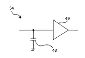
[補正データメモリ34]
補正データを保存するための補正データメモリ34は、画素1行分の補正データを蓄積できるものであれば良い。例えば、画素の列毎に容量を形成して、補正データメモリとしても良い。より望ましくは、図7に示すように、容量48にバッファアンプ49を組み合わせた回路を画素の列毎に設ける。バッファアンプ49を設けることにより、補正データを電流源4のゲートに接続した容量36に移す場合に電荷分配による電圧変化が起きることを防止できる。
【0044】
実施の形態2.
実施の形態1では、各画素センサの直流抵抗成分Raとして寄生抵抗を利用し、画素毎に電流Ifを変化させることで、各画素の電圧降下分If・Raを変化させ、画素センサのオフセット分布を補正した。しかしながら、上記(1)式からわかるように、画素センサ2の寄生抵抗が小さい場合や、補正すべき画素センサ2のオフセット分布が大きな場合には、補正に必要な電流Ifの変化量が大きくなる。電流Ifの画素ごとの変化量があまり大きくなりすぎると、画素センサの感度ばらつきの変化も無視できなくなる。
【0045】
そこで本実施の形態では、オフセット分布を補正するための直流抵抗成分Raとして、各画素センサの寄生抵抗に加えて、各画素センサと電流源の間に挿入した抵抗素子を用いる。即ち、図6に示すように、画素センサ2と電流源4の間に抵抗素子11を挿入し、抵抗素子11と電流源4の間の電位を積分回路7に入力する。このような抵抗素子11を挿入することによって、画素センサ2の寄生抵抗だけを直流抵抗性成分として利用する場合に比べて、より小さな電流Ifの変化量によってオフセット分布を補正することが可能となる。
【0046】
抵抗素子11は、その抵抗温度係数の大きさが画素センサの感度に実施的に影響しない程度に小さなものを用いることが好ましい。また、抵抗素子11の抵抗値は、オフセット分布の補正に必要な電流Ifの変化量が±10%以下、好ましくは±5%以下となるように設定することが望ましい。例えば、電流源の平均電流値が10μAであり、画素センサの出力電圧のばらつきが18mVp−pであった場合、抵抗素子11の抵抗値を18kΩ以上にすれば、オフセット分布に必要な電流Ifの変化量を±10%以下にすることが可能となる。
【0047】
【発明の効果】
本件発明によれば、各画素の電流を制御することによってオフセット分布を積分前に補正するため、積分回路の増幅率を高めて、回路下流にある信号読出回路や信号処理回路で発生する雑音の寄与を小さくすることができる。また、電流による感度変化の少ないダイオードを画素に用い、画素の直流抵抗成分によってオフセット分布を補正するため、感度ばらつきの増加を抑制することができる。
【図面の簡単な説明】
【図1】図1は、本発明の実施の形態1に係る熱型赤外線固体撮像素子を備えた熱型赤外線カメラを示すブロック図である。
【図2】図2は、本発明の実施の形態1における赤外線フォーカルプレーンアレイを示す回路図である。
【図3】図3は、本発明の実施の形態1に係る赤外線フォーカルプレーンアレイの動作状態を示すタイミングチャートである。
【図4】図4(a)及び(b)は、熱型赤外線センサの構造を示す断面図及び斜視図である。
【図5】図5は、ダイオード構造の一例を示す斜視図である。
【図6】図6は、赤外線フォーカルプレーンアレイの信号読出しに用いる積分回路の一例を示す回路図である。
【図7】図7は、補正データメモリの一例を示す回路図である。
【図8】図8は、本発明の実施の形態2に係る熱型赤外線固体撮像素子の一部を示すブロック図である。
【符号の説明】
1 赤外線フォーカルプレーンアレイ、 2 熱型赤外線センサ(画素センサ)、 4 電流源、 7 積分回路、 22 シャッタ、 30 補正データ演算回路、 31 フレームメモリ、 33 補正データ読込み回路、 34 補正データメモリ。[0001]
TECHNICAL FIELD OF THE INVENTION
BACKGROUND OF THE
[0002]
[Prior art]
Thermal infrared cameras are capable of seeing objects that do not stimulate human vision and are capable of instantaneously measuring the temperature of an object from a distance without contact. It is used in a wide variety of forms in a wide range of industrial fields, such as diagnostic devices and human detection devices. A typical thermal infrared camera is configured by combining an infrared focal plane array with an imaging optical system and a signal processing circuit. In the infrared focal plane, thermal infrared sensors for converting a temperature change due to incident infrared rays into electric signals are arranged in a two-dimensional matrix, and the electric signals of the individual thermal infrared sensors are sequentially read out by a peripheral circuit. As a result, a signal corresponding to the infrared image is output.
[0003]
In each of the two-dimensionally arranged thermal infrared sensors, a temperature sensor whose electrical characteristics change according to the temperature is formed. The temperature sensor is lifted in a bridge shape above the substrate by a thin film supporting leg having a high thermal resistance, and is electrically coupled to a signal readout circuit formed on the substrate below the bridge by wiring in the thin film supporting leg. ing. As the temperature sensor, a resistor (= bolometer film) whose resistance changes according to the temperature, or a semiconductor element such as a diode or a transistor is often used.
[0004]
In the infrared focal plane array, for example, a signal is read from each pixel as follows (see Non-Patent
[0005]
However, current-voltage characteristics (for example, forward voltage in a diode type and resistance in a bolometer type) of each pixel arranged in a two-dimensional array vary from pixel to pixel, so that the output signal voltage from the pixel is not constant. Since the output variation for each pixel (hereinafter, “offset distribution”) is relatively large compared to the signal voltage generated by the incidence of infrared rays, fixed pattern noise (hereinafter, “FPN”) occurs in a captured image.
[0006]
Therefore, in an infrared camera using an infrared focal plane array, in order to remove FPN generated by offset distribution, uniform light is incident on the entire pixel array using an optical shutter or the like, and is taken out of the focal plane in that state. The saved FPN data is stored in the storage device. Then, a video signal is formed after the FPN is subtracted from the image signal in a signal processing circuit provided in the infrared camera.
[0007]
Further, in the infrared camera disclosed in
[0008]
[Non-Patent Document 1] Ishikawa, M .; Ueno, K .; Endo, Y .; Nakaki, “Low Cost 320 × 240 Uncooled IRFPA Using Conventional Silicon IC Process”, Par of the SPIE Conference on Infrared Technology and Applications XXV, SPIE Vol. 3698, April 1990, pp. 139-143. 556-564
[Patent Document 1] Japanese Patent No. 321874
[0009]
[Problem to be solved]
In the thermal infrared focal plane array, since the signal is very weak, it is important to reduce noise in order to improve the S / N ratio of an image. In the infrared camera, in addition to the noise of each thermal infrared sensor (= pixel), there are those generated by a signal reading circuit in the infrared focal plane and those generated by a signal processing circuit in the infrared camera. In order to improve the S / N ratio of the image signal, it is desirable to amplify the signal upstream of the circuit system including the signal readout circuit and the signal processing circuit. If the intensity of the image signal is increased upstream of the circuit, the contribution of noise generated downstream can be reduced.
[0010]
However, when high amplification is to be performed in the upstream of the circuit, particularly in the integration circuit in the signal readout circuit, since the image signal includes an offset distribution due to the characteristic variation of each pixel, the offset distribution is also amplified at the same time. . Therefore, when the offset distribution is large, problems such as exceeding the limit voltage of the A / D converter in the signal processing circuit of the camera occur, and the amplification factor cannot be sufficiently increased.
[0011]
The offset distribution of the infrared focal plane array depends on the variation in process parameters when forming the temperature sensor portion and the variation in wiring resistance between pixels in each portion. For example, in the example of the infrared focal plane array shown in
[0012]
On the other hand, according to the signal reading method disclosed in
[0013]
That is, in
[0014]
The present invention has been made in view of the above problems, and removes the FPN due to the offset distribution of each pixel before integration, thereby enabling a high amplification factor in the integration circuit and increasing the sensitivity variation of the pixel. It is an object of the present invention to provide a thermal infrared solid-state imaging device capable of suppressing the occurrence of heat.
[0015]
[Means for Solving the Problems]
In order to achieve the above object, a thermal infrared solid-state imaging device according to the present invention has a heat insulating structure and an infrared absorbing structure, and a pixel area in which a pixel sensor whose current-voltage characteristic changes with temperature is two-dimensionally arranged. A drive line in which the anodes of the pixel sensors are connected in common for each row, a vertical scanning circuit in which the drive lines are sequentially selected and connected to a pixel power source, and a cathode in which the cathodes of the pixel sensors are connected in common in each column, A thermal infrared solid-state imaging device comprising: a signal line having a current source; and an integrating circuit that integrates a voltage between both ends of the current source and outputs the pixel signal as a pixel signal. By using a pixel sensor and changing the current value of the current source for each pixel sensor, the amount of voltage drop due to the DC resistance component of each pixel sensor differs for each pixel sensor, and the pixel of the pixel signal And correcting the variation.
[0016]
In the present specification, a thermal infrared solid-state imaging device refers to a component of a thermal infrared camera that has at least the components described in each claim. Therefore, the thermal infrared solid-state imaging device in the present specification includes an infrared focal plane array, an infrared focal plane array integrated with an external circuit or the like added thereto, or an infrared focal plane and an external circuit etc. Also included modules that are no longer available. The DC resistance component of the pixel sensor is a resistance component that becomes a load when each pixel sensor is driven by a current source, and refers to a DC resistance component generated by factors other than the original diode characteristics such as wiring resistance. In addition to the parasitic resistance of each pixel, a resistance component in a current path from a power supply for driving each pixel sensor to a current source is also included.
[0017]
BEST MODE FOR CARRYING OUT THE INVENTION
Hereinafter, embodiments of the present invention will be described with reference to the drawings.
FIG. 1 is a block diagram showing an infrared camera provided with a thermal infrared solid-state imaging device according to
[0018]
Each
[0019]
The
[0020]
The voltage between both ends of the current source 4 (= the voltage input to the integration circuit 7) Vin is a power supply voltage of VDD [V], a forward voltage of the diode is Vf [V], and the number of connected diodes is n (n is a natural number). If the DC resistance component of the pixel sensor is Ra [Ω] and the value of the current supplied by the
(Equation 1)
![]()
[0021]
In the present embodiment, by changing the current value If of the
[0022]
Further, according to this method, the temperature dependency of the current-voltage characteristic of the diode that contributes to the sensitivity of the
[0023]
For example, the forward voltage Vf [V] of one diode is expressed by the following equation (2), where If [A] is the forward current, k is the Boltzmann constant, q is the elementary charge, and Is is the reverse saturation current. Is done.
(Equation 2)
[Equation 3]
As shown in the above equation (3), the temperature dependency of the forward voltage of the diode that determines the sensitivity of the pixel sensor depends on Vf, and as shown in the above equation (2), Vf is equal to the forward current If. Dependent. However, in general, the forward current If of the diode used in the thermal infrared sensor is orders of magnitude larger than the reverse saturation current Is, and Vf hardly changes with respect to the current If. Therefore, the amount of change in the temperature dependency dVf / dT of the diode forward voltage due to If, which is represented by the above equation (3), becomes negligible, and the sensitivity variation of the pixel sensor is hardly affected by the change in If.
[0025]
On the other hand, as shown in the equation (1), since the voltage Vin input to the
[0026]
A specific method of changing the current value If of the
[0027]
After the signal Vin is integrated and amplified by the
[0028]
For example, for a signal Vin in a state where the shutter is closed, a reference value having a certain voltage width is set, and a routine for evaluating Vin while individually changing If of each pixel is performed. Repeat the routine until it is within the reference value. That is, in the n-th routine, if Vin of a certain pixel is smaller than the reference value, If of the pixel is reduced, and if it is larger than the reference value, If is increased, and If of all pixels is increased. The routine is repeated until Vin falls within the reference value. The step width of If to be changed in one routine may be determined based on the standard value of the parasitic resistance Ra of the pixel. When the influence of the pixel offset distribution is small, each pixel can be simply calculated based on the above equation (1) based on the deviation amount from the reference value of Vin and the standard value of Ra instead of such an algorithm. May be calculated.
[0029]
Information on If of each pixel obtained in this manner is stored in the
(Equation 4)
![]()
Next, general imaging is performed while reading the acquired correction data. That is, at the time of general imaging, after the correction data stored in the
[0031]
The specific configuration and operation of the infrared focal plane including the correction data reading circuit and the correction data memory will be described with reference to FIGS.
FIG. 2 is a circuit diagram showing an example of an infrared focal plane array including a correction data reading circuit and a correction data memory. As shown in FIG. 2, in the infrared
[0032]
A
[0033]
Next, the operation of the infrared focal plane array shown in FIG. 2 will be described. First, the driving lines 3 of each row are sequentially connected to the
[0034]
The
[0035]
The read timing of the output signal of the
[0036]
When the next N-th pixel row is selected, the
[0037]
Hereinafter, each configuration of the infrared focal plane array in the present embodiment will be described in detail.
[Pixel 2]
Each
[0038]
When infrared light enters the
[0039]
The
[0040]
[Integrating circuit 7]
The
[0041]
According to the present invention, since the offset distribution of pixels can be removed before entering the
[0042]
The amplification factor of the
[0043]
[Correction data memory 34]
The
[0044]
In the first embodiment, the parasitic resistance is used as the DC resistance component Ra of each pixel sensor, and the current If is changed for each pixel, so that the voltage drop If · Ra of each pixel is changed. Was corrected. However, as can be seen from the above equation (1), when the parasitic resistance of the
[0045]
Therefore, in the present embodiment, in addition to the parasitic resistance of each pixel sensor, a resistance element inserted between each pixel sensor and the current source is used as the DC resistance component Ra for correcting the offset distribution. That is, as shown in FIG. 6, the
[0046]
It is preferable to use the
[0047]
【The invention's effect】
According to the present invention, since the offset distribution is corrected before integration by controlling the current of each pixel, the amplification factor of the integration circuit is increased to reduce the noise generated in the signal readout circuit and the signal processing circuit located downstream of the circuit. The contribution can be reduced. In addition, since a diode having a small change in sensitivity due to current is used for a pixel and the offset distribution is corrected by a DC resistance component of the pixel, an increase in sensitivity variation can be suppressed.
[Brief description of the drawings]
FIG. 1 is a block diagram showing a thermal infrared camera including a thermal infrared solid-state imaging device according to
FIG. 2 is a circuit diagram showing an infrared focal plane array according to the first embodiment of the present invention.
FIG. 3 is a timing chart showing an operation state of the infrared focal plane array according to the first embodiment of the present invention.
FIGS. 4A and 4B are a cross-sectional view and a perspective view showing the structure of a thermal infrared sensor.
FIG. 5 is a perspective view showing an example of a diode structure.
FIG. 6 is a circuit diagram showing an example of an integration circuit used for signal reading of an infrared focal plane array.
FIG. 7 is a circuit diagram illustrating an example of a correction data memory;
FIG. 8 is a block diagram showing a part of a thermal infrared solid-state imaging device according to
[Explanation of symbols]
1 infrared focal plane array, 2 thermal type infrared sensor (pixel sensor), 4 current source, 7 integration circuit, 22 shutter, 30 correction data operation circuit, 31 frame memory, 33 correction data reading circuit, 34 correction data memory.
Claims (8)
少なくとも1個以上が直列接続されたダイオードを前記画素センサに用い、
前記電流源の電流値を画素センサ毎に変えることにより、各画素センサの有する直流抵抗成分による電圧降下量を画素センサ毎に異ならせ、前記画素信号の画素間ばらつきを補正することを特徴とする熱型赤外線固体撮像装置。A pixel area having a heat insulation structure and an infrared absorption structure, a pixel sensor in which current-voltage characteristics change with temperature is arranged in a two-dimensional manner, a drive line commonly connecting an anode of the pixel sensor for each row, A vertical scanning circuit for sequentially selecting a driving line and connecting to a pixel power supply, a cathode of the pixel sensor commonly connected for each column, and a signal line having a current source at the end thereof; and a voltage across the current source integrated. A thermal infrared solid-state imaging device having an integration circuit that outputs the pixel signal
At least one or more diodes connected in series are used for the pixel sensor,
By changing the current value of the current source for each pixel sensor, the amount of voltage drop due to the DC resistance component of each pixel sensor is made different for each pixel sensor, and the inter-pixel variation of the pixel signal is corrected. Thermal infrared solid-state imaging device.
前記垂直走査回路がN行目(Nは自然数)の駆動線を選択している間に、前記補正データメモリに(N+1)行目の補正データを読込むことを特徴とする請求項1乃至6のいずれか1項に記載の熱型赤外線固体撮像素子。A correction data memory for temporarily storing correction data for determining the current value of the current source for one row of the pixel sensor, and a switch for transferring the correction data stored in the correction data memory to the current source;
7. The correction data of the (N + 1) th row is read into the correction data memory while the vertical scanning circuit is selecting the drive line of the Nth row (N is a natural number). 6. The thermal infrared solid-state imaging device according to claim 1.
Priority Applications (1)
| Application Number | Priority Date | Filing Date | Title |
|---|---|---|---|
| JP2003124796A JP2004336099A (en) | 2003-04-30 | 2003-04-30 | Thermal type infrared solid-state imaging apparatus |
Applications Claiming Priority (1)
| Application Number | Priority Date | Filing Date | Title |
|---|---|---|---|
| JP2003124796A JP2004336099A (en) | 2003-04-30 | 2003-04-30 | Thermal type infrared solid-state imaging apparatus |
Publications (1)
| Publication Number | Publication Date |
|---|---|
| JP2004336099A true JP2004336099A (en) | 2004-11-25 |
Family
ID=33502239
Family Applications (1)
| Application Number | Title | Priority Date | Filing Date |
|---|---|---|---|
| JP2003124796A Pending JP2004336099A (en) | 2003-04-30 | 2003-04-30 | Thermal type infrared solid-state imaging apparatus |
Country Status (1)
| Country | Link |
|---|---|
| JP (1) | JP2004336099A (en) |
Cited By (6)
| Publication number | Priority date | Publication date | Assignee | Title |
|---|---|---|---|---|
| JP2006197338A (en) * | 2005-01-14 | 2006-07-27 | Sony Corp | Solid state imaging device |
| JP2008014766A (en) * | 2006-07-05 | 2008-01-24 | Mitsubishi Electric Corp | Temperature sensor and infrared solid imaging device |
| JP2008531997A (en) * | 2005-02-25 | 2008-08-14 | リッディアルド,ケビン | Microbolometer infrared security sensor |
| WO2011033663A1 (en) * | 2009-09-18 | 2011-03-24 | 株式会社 東芝 | Infrared imaging element |
| CN103076088A (en) * | 2012-12-28 | 2013-05-01 | 西北核技术研究所 | Measuring method of mid-infrared light signal intensity in wide temperature environment |
| US8502872B2 (en) | 2009-03-17 | 2013-08-06 | Mitsubishi Electric Corporation | Infrared solid-state imaging device |
-
2003
- 2003-04-30 JP JP2003124796A patent/JP2004336099A/en active Pending
Cited By (8)
| Publication number | Priority date | Publication date | Assignee | Title |
|---|---|---|---|---|
| JP2006197338A (en) * | 2005-01-14 | 2006-07-27 | Sony Corp | Solid state imaging device |
| JP4613620B2 (en) * | 2005-01-14 | 2011-01-19 | ソニー株式会社 | Solid-state imaging device |
| JP2008531997A (en) * | 2005-02-25 | 2008-08-14 | リッディアルド,ケビン | Microbolometer infrared security sensor |
| JP2008014766A (en) * | 2006-07-05 | 2008-01-24 | Mitsubishi Electric Corp | Temperature sensor and infrared solid imaging device |
| JP4703502B2 (en) * | 2006-07-05 | 2011-06-15 | 三菱電機株式会社 | Temperature sensor and infrared solid-state imaging device |
| US8502872B2 (en) | 2009-03-17 | 2013-08-06 | Mitsubishi Electric Corporation | Infrared solid-state imaging device |
| WO2011033663A1 (en) * | 2009-09-18 | 2011-03-24 | 株式会社 東芝 | Infrared imaging element |
| CN103076088A (en) * | 2012-12-28 | 2013-05-01 | 西北核技术研究所 | Measuring method of mid-infrared light signal intensity in wide temperature environment |
Similar Documents
| Publication | Publication Date | Title |
|---|---|---|
| US7718966B2 (en) | Thermal infrared solid state imaging device and infrared camera | |
| US9609243B2 (en) | Systems and methods for providing low-noise readout of an optical sensor | |
| JP5335006B2 (en) | Infrared solid-state image sensor | |
| JP3866069B2 (en) | Infrared solid-state imaging device | |
| US7397509B2 (en) | High dynamic range imager with a rolling shutter | |
| US20060038900A1 (en) | Image sensor that uses a temperature sensor to compensate for dark current | |
| US20060077273A1 (en) | Low noise active pixel image sensor | |
| JP3226859B2 (en) | Imaging device | |
| JP4009598B2 (en) | Infrared solid-state image sensor | |
| JP2008268155A (en) | Thermal type infrared solid-state imaging element | |
| JP4300635B2 (en) | Solid-state imaging device | |
| US6605806B2 (en) | System and method for generating signals representing infrared radiation | |
| JP2004336099A (en) | Thermal type infrared solid-state imaging apparatus | |
| JP3882594B2 (en) | Solid-state imaging device | |
| JP2002300475A (en) | Infrared sensor and method for driving the same | |
| US20140070075A1 (en) | Radiation detector and method | |
| JP3974902B2 (en) | Thermal infrared detector | |
| JP2009168611A (en) | Infrared solid-state imaging device | |
| US7560694B2 (en) | Method and system for increasing signal-to-noise ratio in microbolometer arrays | |
| JP4320693B2 (en) | Solid-state imaging device | |
| JP3998599B2 (en) | Thermal infrared solid-state imaging device | |
| JP2001218113A (en) | Solid-state image pickup device | |
| JP2004233314A (en) | Thermal type infrared solid-state imaging element | |
| JP2000106651A (en) | Epn correction data generating method and image pickup device using the method | |
| JP4345175B2 (en) | Solid-state imaging device |
Legal Events
| Date | Code | Title | Description |
|---|---|---|---|
| A621 | Written request for application examination |
Free format text: JAPANESE INTERMEDIATE CODE: A621 Effective date: 20051027 |
|
| RD03 | Notification of appointment of power of attorney |
Free format text: JAPANESE INTERMEDIATE CODE: A7423 Effective date: 20080131 |
|
| A977 | Report on retrieval |
Free format text: JAPANESE INTERMEDIATE CODE: A971007 Effective date: 20081015 |
|
| A131 | Notification of reasons for refusal |
Free format text: JAPANESE INTERMEDIATE CODE: A131 Effective date: 20081125 |
|
| A521 | Request for written amendment filed |
Free format text: JAPANESE INTERMEDIATE CODE: A523 Effective date: 20090123 |
|
| A02 | Decision of refusal |
Free format text: JAPANESE INTERMEDIATE CODE: A02 Effective date: 20090303 |