JP2004333723A - Optical element for display, and two-dimensional display device - Google Patents
Optical element for display, and two-dimensional display device Download PDFInfo
- Publication number
- JP2004333723A JP2004333723A JP2003127747A JP2003127747A JP2004333723A JP 2004333723 A JP2004333723 A JP 2004333723A JP 2003127747 A JP2003127747 A JP 2003127747A JP 2003127747 A JP2003127747 A JP 2003127747A JP 2004333723 A JP2004333723 A JP 2004333723A
- Authority
- JP
- Japan
- Prior art keywords
- optical element
- display
- pixels
- display optical
- pixel
- Prior art date
- Legal status (The legal status is an assumption and is not a legal conclusion. Google has not performed a legal analysis and makes no representation as to the accuracy of the status listed.)
- Pending
Links
- 230000003287 optical effect Effects 0.000 title claims abstract description 94
- 230000005484 gravity Effects 0.000 claims abstract description 25
- 239000000835 fiber Substances 0.000 claims abstract description 12
- 239000013307 optical fiber Substances 0.000 claims abstract description 9
- 230000000737 periodic effect Effects 0.000 claims description 16
- 238000002834 transmittance Methods 0.000 claims description 3
- 238000009792 diffusion process Methods 0.000 abstract description 10
- 238000010586 diagram Methods 0.000 description 4
- 238000003384 imaging method Methods 0.000 description 4
- 239000004973 liquid crystal related substance Substances 0.000 description 3
- 230000000694 effects Effects 0.000 description 2
- 238000000034 method Methods 0.000 description 2
- 238000007796 conventional method Methods 0.000 description 1
Images

Abstract
Description
【0001】
【発明の属する技術分野】
本発明は、表示用光学素子おいび2次元表示装置に係り、特に、2次元表示装置に使用される表示用光学素子で、モアレの発生を防止する表示用光学素子に関する。
【0002】
【従来の技術】
近年、液晶表示装置、EL表示装置などのフラットディスプレイが幅広く使用されている(下記、非特許文献参照)。
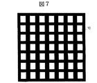
これらのフラットディスプレイでは、図7に示すように、複数の画素10の重心位置が周期的になるように、複数の画素10が配置される。
そのため、従来のフラットディスプレイでは、例えば、グリッド状の物体(例えば、すだれやブラインドなど)越しに、フラットディスプレイを観察すると、重心位置が周期的になるように配置される複数の画素と、グリッド状の物体とが干渉して、モアレ(干渉縞)が発生するという問題点、あるいは、フラットディスプレイをCCDカメラで撮影すると、重心位置が周期的になるように配置される複数の画素と、CCDカメラ内部で周期的に配置されるCCDとが干渉し、CCDカメラで撮影した画像に干渉縞が発生するという問題点があった。
このモアレの発生を防止するために、表示用光学素子の観察者側に拡散板を配置する方法が知られている(下記、特許文献参照)。
【0003】
なお、本願発明に関連する先行技術文献としては以下のものがある。
【非特許文献】
フラットパネルディスプレイ 1992
【特許文献】
特開平10−63199号公報
【0004】
【発明が解決しようとする課題】
しかしながら、前述の特許文献に記載されているような拡散板を用いてモアレの発生を防止する方法は、画像がぼけ表示分解能が低下する、あるいは、光が拡散するので正面の輝度が暗くなってしまうという問題点があった。
本発明は、前記従来技術の問題点を解決するためになされたものであり、本発明の目的は、拡散板を使用することなく、モアレの発生を防止することが可能な表示用光学素子および2次元表示装置を提供することにある。
本発明の前記ならびにその他の目的と新規な特徴は、本明細書の記述及び添付図面によって明らかにする。
【0005】
【課題を解決するための手段】
本願において開示される発明のうち、代表的なものの概要を簡単に説明すれば、下記の通りである。
前述したモアレが発生する理由は、フラットディスプレイなどに使用される表示用光学素子において、複数の画素の重心位置が周期的になるように、複数の画素が配置されていることに原因がある。
そこで、本発明では、フラットディスプレイなどに使用される表示用光学素子において、複数配置される画素の重心位置が非周期的なるようにしたことを最も主要な特徴とする。
即ち、本発明は、複数の画素を有する表示用光学素子であって、前記複数の画素の重心位置が非周期的になるように、前記複数の画素が配置されていることを特徴とする。
【0006】
また、本発明は、複数の画素を備える表示用光学素子であって、前記複数の画素の重心位置が周期的になるように、前記複数の画素が配置されるとともに、前記表示用光学素子の表示面側に配置され、前記複数の画素の重心位置を光学的に非周期的とするシフト光学系を備えることを特徴とする。
本発明の好ましい実施の形態では、前記シフト光学系が、凹凸を有する透明板、凹凸を有する透明板を組み合わせたもの、不均一な屈折率を有する透明板、あるいは、ファイバのある端点の他表面への斜影がもう一方の端点と異なるファイバを含むオプティカルファイバプレートであることを特徴とする。
また、本発明において、表示用光学素子の各画素は、発光素子からなる画素、あるいは、光学特性を制御することにより出射光を制御する画素である。
ここで、光学特性を制御することにより出射光を制御する画素は、散乱度、透過率、吸収率、または、複屈折率を制御することにより出射光を制御する画素である。
また、本発明は、前述の各表示用光学素子を用いる2次元表示装置である。
【0007】
【発明の実施の形態】
以下、図面を参照して本発明の実施の形態を詳細に説明する。
なお、実施の形態を説明するための全図において、同一機能を有するものは同一符号を付け、その繰り返しの説明は省略する。
[実施の形態1]
図1、図2は、本発明の実施の形態1の表示用光学素子の各画素の配置状態の一例を示す図である。
図1、図2に示すように、本実施の形態の表示用光学素子では、複数の画素10の重心位置が非周期的になるように、複数の画素10を配置したことを特徴とする。
これにより、観察者が、本実施の形態の表示用光学素子を使用する2次元表示装置を、グリッド状の物体(例えば、すだれやブラインドなど)越しに観察しても、あるいは、本実施の形態の表示用光学素子を使用する2次元表示装置を、CCDカメラで撮影しても、モアレ(干渉縞)が発生するのを防止することが可能となる。
しかも、本実施の形態では、拡散板を使用しないので、画像がぼけ表示分解能が低下することもなく、あるいは、光が拡散して正面の輝度が暗くなることもない。
ここで、画素10の重心位置とは、例えば、画素の形に切り抜いた紙を、一点で支持したときに、バランスがとれる点である。
【0008】
また、本実施の形態1、あるいは、後述する本実施の形態2の表示用光学素子は、例えば、液晶表示装置、あるいはEL表示装置などに使用される光学素子である。
本実施の形態1、あるいは、後述する本実施の形態2の表示用光学素子が、EL表示装置などに使用される光学素子の場合は、画素10は、発光素子からなる画素となる。
また、本実施の形態1、あるいは、後述する本実施の形態2の表示用光学素子が、液晶表示装置などに使用される光学素子の場合は、画素10は、光学特性を制御することにより出射光を制御する画素となる。
ここで、光学特性を制御することにより出射光を制御する画素は、散乱度、透過率、吸収率、または、複屈折率を制御することにより出射光を制御する画素である。
【0009】
[実施の形態2]
図3は、本発明の実施の形態2の表示用光学素子の他の例を示す要部断面図である。
本実施の形態では、図7に示すように、複数の画素10の重心位置が周期的になるように、表示用光学素子11の複数の画素10が配置される。
しかしながら、本実施の形態では、表示用光学素子11の前面にシフト光学系を配置し、観察者から見た場合に、表示用光学素子11における複数の画素10の重心位置が非周期的になるようにしたものである。
図3に示す表示用光学素子では、このシフト光学系として、凹凸を有する透明板20が使用される。
表示用光学素子11の画素10から出射する光は、凹凸を有する透明板20の表面を通るときに光線が曲げられるので、図3の実線に示すように、複数の画素10の重心位置が周期的になるように、表示用光学素子の複数の画素10が配置されていても、観察者には、図3の破線に示すように、複数の画素10の重心位置が非周期的になるように、表示用光学素子11の複数の画素10が配置されているように感じられる。なお、図3において、実線は実際の画素10の位置を示し、破線は、観察者に感じられる見かけ上の画素10の位置を示す。
これにより、観察者が、図3に示す表示用光学素子を使用する2次元表示装置を、グリッド状の物体(例えば、すだれやブラインドなど)越しに観察しても、あるいは、図3に示す表示用光学素子を使用する2次元表示装置を、CCDカメラで撮影しても、モアレ(干渉縞)が発生するのを防止することが可能となる。しかも、本実施の形態では、拡散板を使用しないので、画像がぼけ表示分解能が低下することもなく、あるいは、光が拡散して正面の輝度が暗くなることもない。
【0010】
図4は、本発明の実施の形態2のシフト光学系の他の例を示す要部断面図である。
図4にシフト光学系は、凹凸を有する透明板20と、凹凸を有する透明板21とを組み合わせたものである。
図4に示す凹凸を有する透明板20と、凹凸を有する透明板21を使用することにより、複数の画素10の重心位置が周期的になるように、表示用光学素子の複数の画素10が配置されていても、観察者には、複数の画素10の重心位置が非周期的になるように、表示用光学素子11の複数の画素10が配置されているように感じられる。
これにより、観察者が、図4に示す表示用光学素子を使用する2次元表示装置を、グリッド状の物体(例えば、すだれやブラインドなど)越しに観察しても、あるいは、図4に示す表示用光学素子を使用する2次元表示装置を、CCDカメラで撮影しても、モアレ(干渉縞)が発生するのを防止することが可能となる。しかも、本実施の形態では、拡散板を使用しないので、画像がぼけ表示分解能が低下することもなく、あるいは、光が拡散して正面の輝度が暗くなることもない。
【0011】
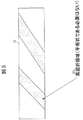
図5は、本発明の実施の形態2のシフト光学系の他の例を示す要部断面図である。
図5に示すシフト光学系は、不均一な屈折率を有する透明板22である。
図5に示す不均一な屈折率を有する透明板22を光が通過する際に、屈折率の変化により光線が曲げられるので、前述の図3の場合と同様、複数の画素10の重心位置が周期的になるように、表示用光学素子の複数の画素10が配置されていても、観察者には、複数の画素10の重心位置が非周期的になるように、表示用光学素子11の複数の画素10が配置されているように感じられる。
これにより、観察者が、図5に示す表示用光学素子を使用する2次元表示装置を、グリッド状の物体(例えば、すだれやブラインドなど)越しに観察しても、あるいは、図5に示す表示用光学素子を使用する2次元表示装置を、CCDカメラで撮影しても、モアレ(干渉縞)が発生するのを防止することが可能となる。しかも、本実施の形態では、拡散板を使用しないので、画像がぼけ表示分解能が低下することもなく、あるいは、光が拡散して正面の輝度が暗くなることもない。
なお、図5では、不均一な屈折率を有する透明板22として、内部に、平板状の高屈折率部分22aを有する透明板を図示しているが、高屈折率部分22aは平板状である必要はなく、また、図5において、高屈折率部分22aは、低屈折率部分であってもよい。
即ち、図5に示す不均一な屈折率を有する透明板22は、透明板の一方から入射される光が、図3、図4に示すような光路を通り、透明板の他方から出射されるものであればよい。
【0012】
図6は、本発明の実施の形態2のシフト光学系の他の例を示す要部断面図である。
図6に示すシフト光学系は、ファイバのある端点の他表面への斜影がもう一方の端点と異なるファイバを含むオプティカルファイバプレート23である。
図6に示すオプティカルファイバプレート23では、オプティカルファイバプレート23を構成する個々のファイバの中で一部のファイバ(例えば、23a,23b)が湾曲している。
そのため、図6の矢印Aの位置から、ファイバ23aに入射する光は、矢印Aとは異なる位置である、図6の矢印Bの位置から出射する。
図6に示すオプティカルファイバプレート23を使用することにより、複数の画素10の重心位置が周期的になるように、表示用光学素子の複数の画素10が配置されていても、観察者には、複数の画素10の重心位置が非周期的になるように、表示用光学素子11の複数の画素10が配置されているように感じられる。
【0013】
これにより、観察者が、図6に示す表示用光学素子を使用する2次元表示装置を、グリッド状の物体(例えば、すだれやブラインドなど)越しに観察しても、あるいは、図6に示す表示用光学素子を使用する2次元表示装置を、CCDカメラで撮影しても、モアレ(干渉縞)が発生するのを防止することが可能となる。しかも、本実施の形態では、拡散板を使用しないので、画像がぼけ表示分解能が低下することもなく、あるいは、光が拡散して正面の輝度が暗くなることもない。
なお、前述の説明において、画素とは、赤、緑、青のサブピクセルの集まりでも、あるいは、赤、緑、青の各サブピクセルであってもよい。
以上、本発明者によってなされた発明を、前記実施の形態に基づき具体的に説明したが、本発明は、前記実施の形態に限定されるものではなく、その要旨を逸脱しない範囲において種々変更可能であることは勿論である。
【0014】
【発明の効果】
本願において開示される発明のうち代表的なものによって得られる効果を簡単に説明すれば、下記の通りである。
本発明によれば、拡散板を使用することなく、観察者が、表示用光学素子または2次元表示装置を、グリッド状の物体越しに観察しても、あるいは、表示用光学素子または2次元表示装置を、CCDカメラで撮影しても、モアレ(干渉縞)が発生するのを防止することが可能となる。
【図面の簡単な説明】
【図1】本発明の実施の形態1の表示用光学素子の各画素の配置状態の一例を示す図である。
【図2】本発明の実施の形態1の表示用光学素子の各画素の配置状態の他の例を示す図である。
【図3】本発明の実施の形態2の表示用光学素子を示す要部断面図である。
【図4】本発明の実施の形態2のシフト光学系の他の例を示す要部断面図である。
【図5】本発明の実施の形態2のシフト光学系の他の例を示す要部断面図である。
【図6】本発明の実施の形態2のシフト光学系の他の例を示す要部断面図である。
【図7】従来のフラットディスプレイの各画素の配置状態を示す図である。
【符号の説明】
10…画素、11…表示用光学素子、20,21…凹凸を有する透明板、22…不均一な屈折率を有する透明板、22a…高屈折率部分、23…オプティカルファイバプレート、23a,23b…ファイバ。[0001]
TECHNICAL FIELD OF THE INVENTION
The present invention relates to a display optical element and a two-dimensional display device, and more particularly to a display optical element used for a two-dimensional display device, which prevents moire from occurring.
[0002]
[Prior art]
2. Description of the Related Art In recent years, flat displays such as liquid crystal display devices and EL display devices have been widely used (see Non-Patent Documents below).
In these flat displays, as shown in FIG. 7, a plurality of
Therefore, in a conventional flat display, for example, when observing a flat display over a grid-shaped object (for example, a blind or a blind), a plurality of pixels arranged such that the position of the center of gravity is periodic and a grid-shaped Of moiré (interference fringes) due to interference with other objects, or a plurality of pixels arranged so that the center of gravity becomes periodic when a flat display is photographed by a CCD camera, and a CCD camera There is a problem that the CCD periodically arranged inside interferes with each other, and interference fringes occur in an image captured by the CCD camera.
In order to prevent the occurrence of moire, there is known a method of disposing a diffusion plate on the viewer side of the display optical element (see Patent Document below).
[0003]
Prior art documents related to the present invention include the following.
[Non-patent literature]
Flat panel display 1992
[Patent Document]
JP-A-10-63199
[Problems to be solved by the invention]
However, the method of preventing the occurrence of moiré by using a diffusion plate as described in the above-mentioned patent document reduces the display resolution of the image by blurring, or the brightness of the front becomes dark because light is diffused. There was a problem that it would.
The present invention has been made in order to solve the problems of the conventional technique, and an object of the present invention is to provide a display optical element and a display optical element which can prevent the occurrence of moire without using a diffusion plate. It is to provide a two-dimensional display device.
The above and other objects and novel features of the present invention will become apparent from the description of the present specification and the accompanying drawings.
[0005]
[Means for Solving the Problems]
The following is a brief description of an outline of typical inventions disclosed in the present application.
The reason why the moiré described above occurs is that a plurality of pixels are arranged in a display optical element used for a flat display or the like such that the positions of the centers of gravity of the plurality of pixels are periodic.
Therefore, the most important feature of the present invention is that the center of gravity of a plurality of arranged pixels is aperiodic in a display optical element used for a flat display or the like.
That is, the present invention is a display optical element having a plurality of pixels, wherein the plurality of pixels are arranged such that the positions of the centers of gravity of the plurality of pixels are non-periodic.
[0006]
Further, the present invention is a display optical element including a plurality of pixels, wherein the plurality of pixels are arranged so that the center of gravity of the plurality of pixels is periodic, and the display optical element A shift optical system is provided on the display surface side and makes the center of gravity of the plurality of pixels optically non-periodic.
In a preferred embodiment of the present invention, the shift optical system includes a transparent plate having irregularities, a combination of transparent plates having irregularities, a transparent plate having a non-uniform refractive index, or another surface of an end point of a fiber. The optical fiber plate is characterized by an optical fiber plate including a fiber having a different angle from the other end point.
Further, in the present invention, each pixel of the display optical element is a pixel composed of a light emitting element or a pixel that controls emitted light by controlling optical characteristics.
Here, a pixel that controls emitted light by controlling the optical characteristics is a pixel that controls emitted light by controlling the degree of scattering, transmittance, absorptance, or birefringence.
Further, the present invention is a two-dimensional display device using each of the above-described display optical elements.
[0007]
BEST MODE FOR CARRYING OUT THE INVENTION
Hereinafter, embodiments of the present invention will be described in detail with reference to the drawings.
In all the drawings for describing the embodiments, components having the same function are denoted by the same reference numerals, and repeated description thereof will be omitted.
[Embodiment 1]
1 and 2 are diagrams illustrating an example of an arrangement state of each pixel of the display optical element according to the first embodiment of the present invention.
As shown in FIGS. 1 and 2, the display optical element of the present embodiment is characterized in that a plurality of
Thereby, even if the observer observes the two-dimensional display device using the display optical element of the present embodiment through a grid-shaped object (for example, a blind or a blind), or the present embodiment It is possible to prevent the occurrence of moire (interference fringes) even when the two-dimensional display device using the display optical element is photographed by a CCD camera.
In addition, in the present embodiment, since the diffusion plate is not used, the image is not blurred and the display resolution is not reduced, or the light is not diffused and the brightness of the front is not darkened.
Here, the position of the center of gravity of the
[0008]
The display optical element according to the first embodiment or a second embodiment described later is an optical element used for, for example, a liquid crystal display device or an EL display device.
When the display optical element according to the first embodiment or the second embodiment described later is an optical element used for an EL display device or the like, the
When the display optical element according to the first embodiment or the second embodiment described later is an optical element used for a liquid crystal display device or the like, the
Here, a pixel that controls emitted light by controlling the optical characteristics is a pixel that controls emitted light by controlling the degree of scattering, transmittance, absorptance, or birefringence.
[0009]
[Embodiment 2]
FIG. 3 is a fragmentary cross-sectional view showing another example of the display optical element according to Embodiment 2 of the present invention.
In the present embodiment, as shown in FIG. 7, the plurality of
However, in the present embodiment, the shift optical system is arranged in front of the display
In the display optical element shown in FIG. 3, a
The light emitted from the
Thereby, even if the observer observes the two-dimensional display device using the display optical element shown in FIG. 3 through a grid-like object (for example, a blind or a blind), or the display shown in FIG. It is possible to prevent moire (interference fringes) from occurring even when a two-dimensional display device using the optical element for imaging is photographed by a CCD camera. In addition, in the present embodiment, since the diffusion plate is not used, the image is not blurred and the display resolution is not reduced, or the light is not diffused and the brightness of the front is not darkened.
[0010]
FIG. 4 is a sectional view of a main part showing another example of the shift optical system according to the second embodiment of the present invention.
In FIG. 4, the shift optical system is a combination of a
By using the
Thereby, even if the observer observes the two-dimensional display device using the display optical element shown in FIG. 4 through a grid-like object (for example, a blind or a blind), or the display shown in FIG. It is possible to prevent moire (interference fringes) from occurring even when a two-dimensional display device using the optical element for imaging is photographed by a CCD camera. In addition, in the present embodiment, since the diffusion plate is not used, the image is not blurred and the display resolution is not reduced, or the light is not diffused and the brightness of the front is not darkened.
[0011]
FIG. 5 is a sectional view of a main part showing another example of the shift optical system according to the second embodiment of the present invention.
The shift optical system shown in FIG. 5 is a
When the light passes through the
Thereby, even if the observer observes the two-dimensional display device using the display optical element shown in FIG. 5 through a grid-like object (for example, a blind or a blind), or the display shown in FIG. It is possible to prevent moire (interference fringes) from occurring even when a two-dimensional display device using the optical element for imaging is photographed by a CCD camera. In addition, in the present embodiment, since the diffusion plate is not used, the image is not blurred and the display resolution is not reduced, or the light is not diffused and the brightness of the front is not darkened.
In FIG. 5, a transparent plate having a flat high
That is, in the
[0012]
FIG. 6 is a sectional view of a main part showing another example of the shift optical system according to the second embodiment of the present invention.
The shift optical system shown in FIG. 6 is an
In the
Therefore, the light incident on the
By using the
[0013]
Thereby, even if the observer observes the two-dimensional display device using the display optical element shown in FIG. 6 through a grid-like object (for example, a blind or a blind), or the display shown in FIG. It is possible to prevent moire (interference fringes) from occurring even when a two-dimensional display device using the optical element for imaging is photographed by a CCD camera. In addition, in the present embodiment, since the diffusion plate is not used, the image is not blurred and the display resolution is not reduced, or the light is not diffused and the brightness of the front is not darkened.
In the above description, the pixel may be a set of red, green, and blue sub-pixels, or each of the red, green, and blue sub-pixels.
As described above, the invention made by the inventor has been specifically described based on the embodiment. However, the present invention is not limited to the embodiment, and can be variously modified without departing from the gist of the invention. Needless to say,
[0014]
【The invention's effect】
The following is a brief description of an effect obtained by a representative one of the inventions disclosed in the present application.
ADVANTAGE OF THE INVENTION According to this invention, even if an observer observes a display optical element or a two-dimensional display apparatus through a grid-shaped object without using a diffusion plate, or a display optical element or a two-dimensional display. Even when the apparatus is photographed by a CCD camera, it is possible to prevent the occurrence of moire (interference fringes).
[Brief description of the drawings]
FIG. 1 is a diagram illustrating an example of an arrangement state of each pixel of a display optical element according to a first embodiment of the present invention.
FIG. 2 is a diagram showing another example of an arrangement state of each pixel of the display optical element according to the first embodiment of the present invention.
FIG. 3 is a cross-sectional view illustrating a main part of a display optical element according to Embodiment 2 of the present invention.
FIG. 4 is a cross-sectional view of a main part showing another example of the shift optical system according to the second embodiment of the present invention.
FIG. 5 is a sectional view of a main part showing another example of the shift optical system according to the second embodiment of the present invention.
FIG. 6 is a sectional view of a main part showing another example of the shift optical system according to the second embodiment of the present invention.
FIG. 7 is a diagram showing an arrangement state of each pixel of a conventional flat display.
[Explanation of symbols]
Reference numeral 10: pixel, 11: display optical element, 20, 21: transparent plate having unevenness, 22: transparent plate having non-uniform refractive index, 22a: high refractive index portion, 23: optical fiber plate, 23a, 23b ... fiber.
Claims (10)
前記複数の画素の重心位置が非周期的になるように、前記複数の画素が配置されていることを特徴とする表示用光学素子。A display optical element including a plurality of pixels,
The display optical element, wherein the plurality of pixels are arranged such that the center of gravity of the plurality of pixels is aperiodic.
前記複数の画素の重心位置が周期的になるように、前記複数の画素が配置され、
前記表示用光学素子の表示面側に配置され、前記複数の画素の重心位置を光学的に非周期的とするシフト光学系を備えることを特徴とする表示用光学素子。A display optical element including a plurality of pixels,
The plurality of pixels are arranged such that the positions of the centers of gravity of the plurality of pixels are periodic,
A display optical element, comprising: a shift optical system that is disposed on a display surface side of the display optical element, and that makes the center of gravity of the plurality of pixels optically non-periodic.
Priority Applications (1)
| Application Number | Priority Date | Filing Date | Title |
|---|---|---|---|
| JP2003127747A JP2004333723A (en) | 2003-05-06 | 2003-05-06 | Optical element for display, and two-dimensional display device |
Applications Claiming Priority (1)
| Application Number | Priority Date | Filing Date | Title |
|---|---|---|---|
| JP2003127747A JP2004333723A (en) | 2003-05-06 | 2003-05-06 | Optical element for display, and two-dimensional display device |
Publications (1)
| Publication Number | Publication Date |
|---|---|
| JP2004333723A true JP2004333723A (en) | 2004-11-25 |
Family
ID=33504138
Family Applications (1)
| Application Number | Title | Priority Date | Filing Date |
|---|---|---|---|
| JP2003127747A Pending JP2004333723A (en) | 2003-05-06 | 2003-05-06 | Optical element for display, and two-dimensional display device |
Country Status (1)
| Country | Link |
|---|---|
| JP (1) | JP2004333723A (en) |
Cited By (6)
| Publication number | Priority date | Publication date | Assignee | Title |
|---|---|---|---|---|
| KR100921483B1 (en) * | 2006-09-29 | 2009-10-13 | 엔이씨 엘씨디 테크놀로지스, 엘티디. | Optical element, and illuminating optical device, display device and electronic device using the same |
| US20110097549A1 (en) * | 2008-06-17 | 2011-04-28 | Koninklijke Philips Electronics N.V. | Appearance-modifying device, method for manufacturing such a device, and appliance covered by such a device |
| CN103278954A (en) * | 2012-11-01 | 2013-09-04 | 上海天马微电子有限公司 | 3D display panel and 3D display device |
| US9601054B2 (en) | 2012-06-08 | 2017-03-21 | Joled Inc. | Display device, manufacturing method, and electronic apparatus |
| JP2018511088A (en) * | 2015-10-09 | 2018-04-19 | リヤード オプトエレクトロニック カンパニー リミテッドLeyard Optoelectronic Co., Ltd. | Image processing method and apparatus used for LED display |
| DE102014109602B4 (en) | 2013-12-19 | 2023-08-03 | Shanghai Tianma Micro-electronics Co., Ltd. | Stereo image display device |
-
2003
- 2003-05-06 JP JP2003127747A patent/JP2004333723A/en active Pending
Cited By (9)
| Publication number | Priority date | Publication date | Assignee | Title |
|---|---|---|---|---|
| KR100921483B1 (en) * | 2006-09-29 | 2009-10-13 | 엔이씨 엘씨디 테크놀로지스, 엘티디. | Optical element, and illuminating optical device, display device and electronic device using the same |
| US8026880B2 (en) | 2006-09-29 | 2011-09-27 | Nec Lcd Technologies, Ltd | Optical element, and illuminating optical device, display device and electronic device using the same |
| US20110097549A1 (en) * | 2008-06-17 | 2011-04-28 | Koninklijke Philips Electronics N.V. | Appearance-modifying device, method for manufacturing such a device, and appliance covered by such a device |
| US8693086B2 (en) * | 2008-06-17 | 2014-04-08 | Koninklijke Philips N.V. | Appearance-modifying device, method for manufacturing such a device, and appliance covered by such a device |
| US9601054B2 (en) | 2012-06-08 | 2017-03-21 | Joled Inc. | Display device, manufacturing method, and electronic apparatus |
| CN103278954A (en) * | 2012-11-01 | 2013-09-04 | 上海天马微电子有限公司 | 3D display panel and 3D display device |
| CN103278954B (en) * | 2012-11-01 | 2016-03-30 | 上海天马微电子有限公司 | A kind of 3D display panel and 3D display device |
| DE102014109602B4 (en) | 2013-12-19 | 2023-08-03 | Shanghai Tianma Micro-electronics Co., Ltd. | Stereo image display device |
| JP2018511088A (en) * | 2015-10-09 | 2018-04-19 | リヤード オプトエレクトロニック カンパニー リミテッドLeyard Optoelectronic Co., Ltd. | Image processing method and apparatus used for LED display |
Similar Documents
| Publication | Publication Date | Title |
|---|---|---|
| US8891030B2 (en) | Display method, display apparatus, optical unit, method of manufacturing display apparatus, and electronic equipment | |
| US8390671B2 (en) | Display with gaps for capturing images | |
| JP2017194695A (en) | Stereoscopic display apparatus | |
| KR101404536B1 (en) | 3d image display optical member and 3d image display device | |
| US8619367B2 (en) | Display apparatus, display unit, electronic equipment, mobile electronic equipment, mobile telephone, and image pickup apparatus | |
| JP5558001B2 (en) | Display device with function to homogenize attenuation filter | |
| CN102959455B (en) | The viewing auxiliary equipment of 3D three-dimensional display | |
| TW201403177A (en) | Displaying apparatus | |
| KR0146619B1 (en) | Video device utilizing a two-dimensional diffraction grating | |
| JP2006309002A (en) | Optical film without moire fringe, applied to backlight for liquid crystal display device | |
| JP5144508B2 (en) | Image display device | |
| JP2008216340A (en) | Stereoscopic and planar images display device | |
| JP4490357B2 (en) | Video presentation / imaging device | |
| JP2004333723A (en) | Optical element for display, and two-dimensional display device | |
| EP1083756A2 (en) | Stereoscopic image display apparatus | |
| JP2016206512A (en) | Head-mounted display | |
| JP5603635B2 (en) | Display unit, display device, electronic device, portable electronic device, mobile phone, and imaging device | |
| WO2006020583A3 (en) | Imaging material with improved contrast | |
| JP2009145855A (en) | Display device | |
| JP4698616B2 (en) | Image display device and portable terminal device using the same | |
| JP2011170277A (en) | Display method, display device, optical unit, and electronic equipment | |
| JP3877704B2 (en) | 3D display device | |
| JP3816463B2 (en) | Display optical element and two-dimensional display device | |
| WO2013046914A1 (en) | Multiprojection system | |
| JP2004336290A (en) | Three-dimensional display device |
Legal Events
| Date | Code | Title | Description |
|---|---|---|---|
| A621 | Written request for application examination |
Free format text: JAPANESE INTERMEDIATE CODE: A621 Effective date: 20040930 |
|
| A977 | Report on retrieval |
Free format text: JAPANESE INTERMEDIATE CODE: A971007 Effective date: 20060221 |
|
| A131 | Notification of reasons for refusal |
Free format text: JAPANESE INTERMEDIATE CODE: A131 Effective date: 20060704 |
|
| A02 | Decision of refusal |
Free format text: JAPANESE INTERMEDIATE CODE: A02 Effective date: 20061031 |