JP2004318092A - Image forming apparatus and image forming method using it - Google Patents
Image forming apparatus and image forming method using it Download PDFInfo
- Publication number
- JP2004318092A JP2004318092A JP2004076543A JP2004076543A JP2004318092A JP 2004318092 A JP2004318092 A JP 2004318092A JP 2004076543 A JP2004076543 A JP 2004076543A JP 2004076543 A JP2004076543 A JP 2004076543A JP 2004318092 A JP2004318092 A JP 2004318092A
- Authority
- JP
- Japan
- Prior art keywords
- developing roller
- image forming
- developing
- image
- toner
- Prior art date
- Legal status (The legal status is an assumption and is not a legal conclusion. Google has not performed a legal analysis and makes no representation as to the accuracy of the status listed.)
- Pending
Links
Images

Landscapes
- Magnetic Brush Developing In Electrophotography (AREA)
- Developing For Electrophotography (AREA)
- Dry Development In Electrophotography (AREA)
Abstract
Description
本発明は、電子写真方式を利用した複写機、プリンタまたはファクシミリ、もしくはそれらの複合機などの画像形成装置および画像形成方法に関し、より詳しくは、磁性キャリアを用いて非磁性のトナーを帯電させる二成分現像剤を使用し、磁気ローラの表面にこの2成分現像剤を担持し、現像剤中の帯電されたトナーのみを現像ローラ上に移行させて、そのトナーを静電潜像に飛翔させることで該潜像を現像する非接触現像方式の画像形成装置とそれを用いる画像形成方法に関する。 The present invention relates to an image forming apparatus and an image forming method such as a copying machine, a printer, a facsimile, or a multifunction machine using an electrophotographic method, and more particularly, to a method of charging a non-magnetic toner using a magnetic carrier. Using a two-component developer on the surface of a magnetic roller using a two-component developer, transferring only the charged toner in the developer onto the developing roller, and causing the toner to fly to an electrostatic latent image The present invention relates to a non-contact developing type image forming apparatus for developing the latent image and an image forming method using the same.
従来、この種の二成分現像剤を用いる、静電潜像を担持した像担持体に対向した現像ローラと、現像ローラに関して像担持体の反対側に現像ローラと離間して配置された磁気ローラを有する、所謂ハイブリッド現像装置を有する画像形成装置は、特許文献1あるいは特許文献2等に開示のとおり既に公知である。近年は、高速のカラー画像形成方式として、特に感光体上に複数の色に対応した帯電器や露光光学系や現像器等からなる画像形成部を複数設け、カラー画像を順次形成する1ドラム色重ね方式用としても検討されてきた。この方式によると感光体上に正確にトナーを重ねることで色ズレの少ないカラー画像形成が可能であり、カラーの高画質化に対応する技術として注目されている。このようなカラー画像形成装置において、上述の現像方式が他の色の画像形成部によって形成されたトナー像を乱さない現像方式として注目されている。さらに最近になって、高速化をトナーの色に対応した複数の感光体を用いて、転写部材の送りに同期させてカラー画像を形成し転写部材上で色重ねを行うタンデム方式において、接触することによって感光体に余計な付加を与えることのない非接触現像方式として上述の現像方式が注目されてきている。
Conventionally, using a two-component developer of this type, a developing roller facing an image carrier carrying an electrostatic latent image, and a magnetic roller disposed on the opposite side of the image carrier with respect to the developing roller and spaced apart from the developing roller An image forming apparatus having a so-called hybrid developing device is already known as disclosed in Patent Document 1 or
この現像方式の場合、現像剤中に現像されない微粉や外添剤等が含まれることが現像性を落とす原因となる。そこで、現像性を向上させるために現像ローラと感光体ドラムとの間隔を狭くしたり、ACピーク電圧(Vpp)を高くしたりすると、その間において印加電位のリークが発生する。この結果、二成分現像剤のうちキャリアを移動させずに、十分帯電したトナーのみを現像ローラへ移動させるという目的を充分に果たせなくなる。
そこで、本発明の目的は、磁気ローラのトナーとキャリアによる磁気ブラシを介して現像ローラ表面に形成されるトナー薄層によって感光体上の静電潜像を現像して画像を形成する画像形成装置において、現像ローラと感光体ドラム間における印加電圧のリークを抑えるために有効な画像形成装置とそれを用いる画像形成方法を提供することにある。 Therefore, an object of the present invention is to provide an image forming apparatus that forms an image by developing an electrostatic latent image on a photoreceptor with a thin toner layer formed on the surface of a developing roller via a magnetic brush of toner and a carrier of a magnetic roller. SUMMARY OF THE INVENTION An object of the present invention is to provide an image forming apparatus effective for suppressing leakage of an applied voltage between a developing roller and a photosensitive drum and an image forming method using the same.
上記課題を解決するために、本発明者らは、まず現像ローラを構成する材質の検討を行なって、アルミ素管を選択しさらにその表面にアルミニウムの酸化皮膜処理を施した現像ローラを用いることにより、感光体ドラムとの間における印加電圧のリーク防止に有効であるとの知見を得た。さらに、このアルミニウムの酸化皮膜処理を施した現像ローラと感光体ドラム素管との間隔と印加電圧リークとの関係を検討したところ、150〜300μmに設定することが極めて有効であるとの知見も得た。このときのアルミニウムの酸化皮膜は、厚みを5μm以上にするときに、印加電圧リークがよく防止される。 In order to solve the above-mentioned problems, the present inventors first examined the material constituting the developing roller, selected an aluminum pipe, and used a developing roller having its surface subjected to an aluminum oxide film treatment. As a result, the present inventors have found that it is effective in preventing leakage of an applied voltage between the photosensitive drum and the photosensitive drum. Further, when the relationship between the distance between the developing roller subjected to the aluminum oxide film treatment and the photosensitive drum tube and the applied voltage leak was examined, it was found that setting the distance to 150 to 300 μm was extremely effective. Obtained. When the thickness of the aluminum oxide film at this time is set to 5 μm or more, applied voltage leakage is well prevented.
一方、上記の画像形成装置を用いて現像するに際して、現像ローラから感光体へトナーを飛翔させるために現像ローラへ交流電圧を印加させるときに、非画像形成時における交流電流の周波数を画像形成時よりも大きくなるように制御すれば、非現像時におけるキャリア引きを抑制する効果があるとの知見を得た。
本発明は、これらの知見に基づいてさらに検討して完成されたものであり、以下の画像形成装置およびそれを用いる画像形成方法に関する。
On the other hand, when developing using the above-described image forming apparatus, when applying an AC voltage to the developing roller in order to cause toner to fly from the developing roller to the photosensitive member, the frequency of the AC current during non-image formation is changed during image formation. It has been found that if the control is made to be larger than the above, there is an effect of suppressing carrier pulling during non-development.
The present invention has been completed by further study based on these findings, and relates to the following image forming apparatus and an image forming method using the same.
1)磁気ローラのトナーとキャリアによる磁気ブラシを介して現像ローラ表面に形成されるトナー薄層によって感光体上の静電潜像を現像して画像を形成する画像形成装置において、
前記現像ローラがアルミ製でありその表面に厚みが少なくとも5μmのアルミニウムの酸化皮膜を形成させ、かつ前記現像ローラと感光体ドラム素管との間隔を150〜300μmに設定してなることを特徴とする画像形成装置。
1) In an image forming apparatus for forming an image by developing an electrostatic latent image on a photoreceptor with a thin toner layer formed on the surface of a developing roller through a magnetic brush made of a toner and a carrier of a magnetic roller,
The developing roller is made of aluminum, an oxide film of aluminum having a thickness of at least 5 μm is formed on the surface thereof, and the interval between the developing roller and the photosensitive drum tube is set to 150 to 300 μm. Image forming apparatus.
2)前記アルミニウムの酸化皮膜の厚みが10〜20μmであり、現像ローラと感光体ドラム素管との間隔が150〜280μmである上記1)項記載の画像形成装置。
3)磁気ローラのトナーとキャリアによる磁気ブラシを介して現像ローラ表面に形成されるトナー薄層によって感光体上の静電潜像を現像して画像を形成するに際して、
前記現像ローラがアルミ製でありその表面に厚みが少なくとも5μmのアルミニウムの酸化皮膜を形成し、かつ前記現像ローラと感光体ドラム素管との間隔を150〜300μmに設定してなる画像形成装置を用いて、
前記現像ローラには交流電圧が重畳された直流電圧が印加され、
静電潜像の現像時の前記直流電流の周波数よりも非現像時における前記交流電流の周波数以上になるように制御し、帯電されたトナーを選択的に静電潜像に飛翔させながら現像すること特徴とする画像形成方法。
2) The image forming apparatus according to 1) above, wherein the thickness of the aluminum oxide film is 10 to 20 μm, and the distance between the developing roller and the photosensitive drum base is 150 to 280 μm.
3) When forming an image by developing an electrostatic latent image on a photoreceptor with a thin toner layer formed on the surface of a developing roller through a magnetic brush of toner and a carrier of a magnetic roller,
An image forming apparatus, wherein the developing roller is made of aluminum, an oxide film of aluminum having a thickness of at least 5 μm is formed on the surface thereof, and an interval between the developing roller and the photosensitive drum tube is set to 150 to 300 μm. make use of,
A DC voltage on which an AC voltage is superimposed is applied to the developing roller,
Control is performed so that the frequency of the direct current at the time of development of the electrostatic latent image is higher than the frequency of the alternating current at the time of non-development, and the charged toner is developed while selectively flying on the electrostatic latent image. An image forming method.
4)前記の現像時における周波数を1〜4kHzとする上記3)項記載の画像形成方法。
5)前記の現像時における周波数を1〜3kHzとする上記3)項記載の画像形成方法。
6)前記の非現像時における周波数を4〜8kHzとする上記3)高記載の画像形成方法。
4) The image forming method according to the above item 3), wherein the frequency during the development is 1 to 4 kHz.
5) The image forming method according to the above item 3), wherein the frequency during the development is 1 to 3 kHz.
6) The image forming method described in 3) above, wherein the frequency at the time of non-development is 4 to 8 kHz.
7)前記の非現像時における周波数を5〜8kHzとする上記3)項記載の画像形成方法。
本発明において、アルミ製の現像ローラの表面に形成するアルミニウムの酸化皮膜は、印加電圧リークを防止するために、厚みを5μm以上とするが、好ましくは10μm以上である。厚みの上限は特に限定されないが、20μm程度で十分であり、これよりも厚くするとコストが高くなるだけで効果上、差がなくなる。
7) The image forming method as described in 3) above, wherein the frequency at the time of non-development is 5 to 8 kHz.
In the present invention, the aluminum oxide film formed on the surface of the aluminum developing roller has a thickness of 5 μm or more, preferably 10 μm or more, in order to prevent an applied voltage leak. The upper limit of the thickness is not particularly limited, but about 20 μm is sufficient. If the thickness is larger than this, only the cost increases, and there is no difference in effect.
画像形成時(現像時)の周波数は、あまり高くすればゴースト画像が悪くなることから一般に1〜3kHz付近で行なわれている。しかしながら、この周波数設定では、非現像時においてキャリアが磁気ブラシから現像ローラ上に移り、それが感光体ドラム上にも移動するという、いわゆるキャリア引きが発生する。そこで、本発明の画像形成方法においては、上記の画像形成装置を用いて、非現像時の周波数を好ましくは4〜8kHzとすることにより、キャリア引き防止を達成したものである。 The frequency at the time of image formation (at the time of development) is generally set to around 1 to 3 kHz since a ghost image becomes worse if the frequency is too high. However, with this frequency setting, so-called carrier pulling occurs in which the carrier moves from the magnetic brush onto the developing roller during non-development, and moves on the photosensitive drum. Therefore, in the image forming method of the present invention, the carrier is prevented from being pulled by setting the frequency during non-development to preferably 4 to 8 kHz using the above image forming apparatus.
本発明によると、磁気ローラのトナーとキャリアによる磁気ブラシを介して現像ローラ表面に形成されるトナー薄層によって感光体上の静電潜像を現像して画像を形成する画像形成装置において、現像ローラと感光体ドラム間における印加電圧のリークを抑え、良好な画像特性の画像を得るのに有効な現像手段が提供される。
According to the present invention, in an image forming apparatus for forming an image by developing an electrostatic latent image on a photoreceptor with a thin toner layer formed on the surface of a developing roller through a magnetic brush of toner and a carrier of a magnetic roller, There is provided a developing means effective for suppressing leakage of an applied voltage between the roller and the photosensitive drum and obtaining an image having good image characteristics.
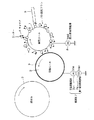
本発明の画像形成装置における現像を中心としたシステム構成を、図1および2を参照しつつ説明する。
図1において、感光体3と現像ローラ2を配設し、該現像ローラ2から所定間隔をおいて非磁性金属材料で円筒状に形成され、円筒内には複数の固定磁石が配設されて、該固定磁石の周囲を回転可能に構成されたスリーブを有した磁気ローラ1が配設されている。
A system configuration focusing on development in the image forming apparatus of the present invention will be described with reference to FIGS.
In FIG. 1, a
10a、10bはパドルミキサー、感光体1と現像ローラ2との間には現像バイアス電圧DC7aとAC7bが印加され、磁気ローラ1には現像バイアス電圧DC8が印加される(図2参照)。9は磁気ブラシの厚さを制御する規制ブレードであり、本発明では規制ブレード9と磁気ローラ1表面との間のギャップは0.45〜0.65mmの範囲であることが好ましい。
10a and 10b are paddle mixers, and developing bias voltages DC7a and AC7b are applied between the photosensitive member 1 and the developing
次に、感光体3と、現像装置内の磁気ローラ1と、現像ローラ2との作用を説明する。
図2に示すように、この磁気ローラ1は、トナー5を帯電させて保持するキャリア4による磁気ブラシ10を発生させる。また、現像ローラ2の表面には、磁気ブラシ10から供給されたトナー5によりトナー薄層6が形成される。そして、感光体3は、トナー薄層6のトナーを静電潜像に応じて選択的に飛翔させて画像形成を行なう。この画像が、1次転写ローラ13との間を通過する印刷体14に転写される。本発明におけるキャリア粒径の好適な範囲は35〜50μmである。
Next, the operation of the
As shown in FIG. 2, the magnetic roller 1 generates a magnetic brush 10 by a carrier 4 that charges and holds a toner 5. A
感光体3としては、正帯電有機感光体(正OPC)がオゾンなどの発生が少なく帯電が安定しており、特に単層構造の正OPCは長期にわたって使用し膜厚が変化した場合においても、感光特性に変化が少なく画質も安定するため、長寿命のシステムにおいて最適である。これに加えて、a−Si感光体も用いることもできる。
長寿命のシステムとする場合、正OPCの膜厚を20μmから40μm程度に設定するのが有利である。正OPCは、画像形成に使用するときに膜厚が減少して10μmに達すると絶縁破壊によって黒点の発生が目だってくることからこれを防ぐ意味で20μm以上に設定することが好ましいが、40μmを超えると感度が低下し画質低下の要因と成り易くなる。
As the
In the case of a long-life system, it is advantageous to set the thickness of the positive OPC to about 20 to 40 μm. The positive OPC is preferably set to 20 μm or more in order to prevent black spots from being generated due to dielectric breakdown when the film thickness decreases to 10 μm when used for image formation and reaches 10 μm. If it exceeds, the sensitivity is lowered, which tends to cause the image quality to be lowered.
露光装置11は、半導体レーザーもしくはLEDを用いたシステムが適当である。この場合、正OPCでは770nm付近の波長が有効であり、a−Si感光体では685nm付近の波長が有効である。以下、正OPC用いた場合を例に挙げて説明する。
帯電装置12によって静電潜像担持体である正OPC3を400Vに帯電する。その後、770nmの波長のLEDによって露光を行うと露光後電位は70Vに設定される。正OPC3は現像ローラ2に対し、約250μmの空間をもって配置される。この空間にはワイヤー電極等は用いない。
As the
The charging
本発明において、現像ローラ2の表面は導電性のアルミニュウムからなる回転体である。現像ローラ2と磁気ローラ1の電位差にて現像ローラ2にトナー薄層を形成する。電位差は、現像ローラの電位を70V、磁気ローラの電位を400Vにすることで、現像ローラ2に約1〜1.5mg/cm2のトナー層が形成される。この時のトナーの帯電量は、約10〜20μC/gが適正であり、10μC/gに達しないときはトナー飛散が目立ち、20μC/gを超えると薄層形成されたトナーが感光体3へ飛翔し難くなる。
In the present invention, the surface of the developing
現像ローラ2から感光体3へとトナーを飛翔させるために現像ローラへ交流電圧を印加することで現像性が高められる。電圧としては、P−P=1.5KV、f=3.0kHzで画像濃度・ドット再現・カブリ除去のバランスをとることができる。また、DUTY比(現像ローラに印加する交流電圧のDUTY比で、トナーが感光体側に移動するような電圧を現像ローラに印加する時間をa、トナーが感光体と反対方向(即ち現像ローラ方向)に移動するような電圧を現像ローラに印加する時間をbとして、duty比=a/(a+b)(×100)%)は30%にすることで現像ゴーストの発生を抑制することができる。
By applying an AC voltage to the developing roller in order to cause the toner to fly from the developing
現像ローラ2のトナー層表面越しの電位を測定すると約320Vとなっており、320V−70V(全露光後感光体電位)=250Vが実質の現像の実行電位であるといえる。
磁気ローラ1と現像ローラ2とのギャップは、通常400μmに設定されており、規制ブレード9と磁気ローラ1のギャップはキャリアの粒径に応じて調整される。例えば、平均粒径35μmのキャリアとトナー10%の現像剤においては350〜500μmに設定し、磁気ブラシが現像ローラ2に接触する設定とする。現像ローラ2と磁気ローラ1のギャップが狭すぎると現像剤がローラ間を通過できずに溢れてしまい、広すぎると現像ローラに接触できず現像ローラのトナーを回収することが困難になり、現像動作を繰り返すと次第に現像ローラ2にトナーが固着してしまい、感光体3にトナーが飛翔できなくなってしまう。
When the potential of the developing
The gap between the magnetic roller 1 and the developing
本発明においては、感光体ドラム素管3と現像ローラ2との間隔は、150〜300μmに設定される。具体的には、印加電位リークと現像性能をみながら調整する。この間隔を上記の範囲よりも狭くすると、現像性が上がり現像器中の微粉の上昇も抑えられ、長寿命化の面からみれば効果的である。しかしながら、あまりに狭くすると印加電位リークに関する余裕度が狭くなるという問題がでてくる。
In the present invention, the distance between the
本発明では、現像性と印加電位リーク防止の関係を満足させるために、まず現像ローラの材質にアルミを採用し、その表面に厚み5μm以上のアルミニウムの酸化皮膜が施されている。アルミニウムの酸化皮膜を5μm以上にすることによって印加電位リーク防止に効果があり、10μm以上であればさらに好ましい。厚みの上限値は、印加電位リークを防止する目的上は20μmでよく、それを超えて厚くすることはコスト的に不利になる。 In the present invention, in order to satisfy the relationship between the developability and the prevention of applied potential leak, aluminum is first used as the material of the developing roller, and the surface thereof is coated with an aluminum oxide film having a thickness of 5 μm or more. Making the aluminum oxide film 5 μm or more is effective in preventing applied potential leakage, and more preferably 10 μm or more. The upper limit of the thickness may be 20 μm for the purpose of preventing leakage of the applied potential, and increasing the thickness beyond that is disadvantageous in cost.
次に、本発明の画像形成装置を用いて現像を行なう際には、現像ローラから感光体ドラムへトナーを飛翔させるために現像ローラへ交流電圧を印加させるときに、非現像時の交流電流の周波数を静電潜像の現像時における周波数以上となるように制御する。なお、ここで非現像時とは現像ローラ回転中で且つ感光体ドラムが帯電されている時間の内、静電潜像が現像されている時間を除いた時間である。 Next, when developing using the image forming apparatus of the present invention, when applying an AC voltage to the developing roller in order to cause the toner to fly from the developing roller to the photosensitive drum, The frequency is controlled so as to be higher than the frequency at the time of developing the electrostatic latent image. Here, the non-development time is the time during which the developing roller is rotating and the photosensitive drum is charged, excluding the time during which the electrostatic latent image is being developed.
その結果、二成分現像剤のうちキャリアを移動させずに、十分帯電したトナーのみを現像ローラへ移動させるという本現像方式の目的を良好に達成することができる。前記の現像時における交流電圧(交番電界)周波数は1〜4kHzとすることが好ましく、1〜3kHzとすることがより好ましい。また非現像時における交流電圧の周波数は、3.5〜8kHzであることが好ましく、3.5〜7kHzとすることがより好ましい。より具体的には、非現像時におけるスリ−ブDCを100V以下で使用する場合には4〜8kHz以上とし、100〜200Vで使用する場合は5〜8kHz以上とするのが好ましい。 As a result, the purpose of the present development system of moving only the sufficiently charged toner to the developing roller without moving the carrier among the two-component developer can be achieved favorably. The AC voltage (alternating electric field) frequency during the development is preferably 1 to 4 kHz, more preferably 1 to 3 kHz. Further, the frequency of the AC voltage during non-development is preferably 3.5 to 8 kHz, more preferably 3.5 to 7 kHz. More specifically, when the sleeve DC at the time of non-development is used at 100 V or less, the frequency is preferably 4 to 8 kHz or more, and when it is used at 100 to 200 V, the frequency is preferably 5 to 8 kHz or more.
アルミ製現像ローラの表面にアルミニウムの酸化皮膜を形成することは、それ自体公知方法により実施することができる。すなわち、アルミ製ローラを陽極にして、硫酸、しゅう酸、クロム酸などの浴中で電解すると、陽極に発生する酸素のためにアルミニウムの表面に、多孔質であるが電気絶縁性が高く、耐食性、耐摩耗性の酸化皮膜を形成することができる。 The formation of an aluminum oxide film on the surface of the aluminum developing roller can be performed by a method known per se. In other words, when an aluminum roller is used as an anode and electrolyzed in a bath of sulfuric acid, oxalic acid, chromic acid, etc., due to oxygen generated at the anode, the aluminum surface is porous but has high electrical insulation and corrosion resistance. And a wear-resistant oxide film can be formed.
以下、実施例により本発明を更に詳細に説明するが、これらは本発明の一例を説明したものであり、本発明の範囲はかかる記載に限定されるものではない。
(実施例1〜9および比較例1〜4)
図1に示した現像を中心としたシステム構成において、感光体ドラム素管3と現像ローラ2との距離を180μmに設定した。現像ローラに印加するDC電圧を100Vとし、Vpp(AC印加した場合のもので、電圧の最大値と最小値との差の電圧)を1.4〜1.7kVで行った。周波数は現像時には3kHzに、非現像時には6kHzとなるように制御した。
Hereinafter, the present invention will be described in more detail by way of examples. However, these are merely examples of the present invention, and the scope of the present invention is not limited to the description.
(Examples 1 to 9 and Comparative Examples 1 to 4)
In the system configuration centering on development shown in FIG. 1, the distance between the
表1に、アルミニウムの酸化皮膜の厚みと10枚白画像連続通紙した場合の紙面上リーク点の数との関係を示した。ここで、リーク点は、白紙画像を10枚連続通紙した後、紙面上のリーク点を数えて測定した。感光体に対してリークが起きると感光層が絶縁破壊され帯電できなくなるため黒点(リーク点)が現れる。なお、感光体ドラム素管3の周速は100mm/s、現像ローラの周速は150mm/s、磁気ローラ1の周速は225mm/sに設定した。また現像剤中のトナー濃度が10%に維持できるように制御した。
Table 1 shows the relationship between the thickness of the aluminum oxide film and the number of leak points on the paper surface when 10 white images were continuously passed. Here, the leak point was measured by counting the number of leak points on the paper surface after continuously passing 10 blank paper images. If a leak occurs to the photoconductor, the photosensitive layer is destructed and cannot be charged, so that a black point (leak point) appears. The peripheral speed of the

この結果、アルミローラ上にアルミニウムの酸化皮膜を形成することにより、リークの発生が解消されていることがわかる。ここで、酸化皮膜の厚み5μmでは、Vppを1.5kVまではリークが抑えられるが、1.6kV以上に上げるとリークが発生する。酸化皮膜10μm以上にすることによって、実用上の使用電圧である1.4kVから1.7kVにおいてリークをよく抑えることができた。 As a result, it can be understood that the occurrence of the leak is eliminated by forming the aluminum oxide film on the aluminum roller. Here, when the thickness of the oxide film is 5 μm, the leak can be suppressed up to Vpp of 1.5 kV, but when Vpp is increased to 1.6 kV or more, the leak occurs. By setting the oxide film to 10 μm or more, the leakage was successfully suppressed at a practical working voltage of 1.4 kV to 1.7 kV.
表2はアルミニウムの酸化皮膜の厚さを10μm、Vppを1.7kVとし、他の実験条件は表1の場合と同じに設定して、感光体ドラム素管3と現像ローラ2の間のギャップ(間隔)とリーク点の発生の関係を示した。ギャップを130μmとすると酸化被膜の厚さを20μm、Vppを1.4kVとしてもリーク点が12点発生したことから、リーク点を発生させないためには、間隔は150μm以上必要であることが判明した。また間隔を320μmとすると画像濃度が規定の1.30より低い1.24まで低下した。したがって画像濃度を規定値以上にするためには、間隔は300μm以下であることが必要であると判明した。なお画像濃度はマクベス社製の反射濃度計RD−918を用いて測定した。
Table 2 shows that the thickness of the oxide film of aluminum was 10 μm, Vpp was 1.7 kV, and the other experimental conditions were the same as those in Table 1, and the gap between the
*1:酸化被膜を20μm、Vppを1.4KVとしてもリーク点が10点発生
*2:画像濃度が規定値(1.3)以下の1.24となり、線画像の再現性が悪い。
次に、表3には現像時に現像ローラに印加する交流の周波数と画像品質との関係を示した。この場合、アルミニウムの酸化皮膜の厚さを20μm、感光体ドラム素管3と現像ローラ2との距離を180μm、交流電圧のVppを1.6kV、非現像時に現像ローラに印加する交流の周波数は6kHzに設定した。周波数が0.5kHzとなると、画像濃度が規定値の1.30以下となり、周波数を4.0kHzとするとゴ−スト画像が発生しだし、周波数が5kHzでは現像ローラに印加する直流電圧にかかわらずゴースト画像が目立つようになる。したがって、現像時の交流の周波数は1〜4kHzであることが好ましく、1〜3kHzであることがより好ましいことがわかる。なお、ゴースト画像の評価は用紙の搬送方向に対してベタ黒画像の次にベタ黒画像より用紙搬送方向の長さの長いハーフトーン画像が来るように設定し、ベタ黒画像とハーフトーン画像の先端の間隔を現像ローラ2の周長に設定する。ゴースト現象が発生するとハーフトーン画像に黒い影状の不必要な画像が生じるので、ゴースト現象の発生の有無が判断できる。
* 1: Even when the oxide film is 20 μm and Vpp is 1.4 KV, 10 leak points are generated. * 2: The image density is 1.24 which is equal to or less than the specified value (1.3), and the reproducibility of the line image is poor.
Next, Table 3 shows the relationship between the frequency of the AC applied to the developing roller during development and the image quality. In this case, the thickness of the aluminum oxide film is 20 μm, the distance between the
上記における評価基準は、次のとおりである。
×:画像濃度が1.30未満または目視でゴーストが明確にわかるもの
△:画像濃度が1.30〜1.35または目視でゴーストが若干わかるもの
○:良好(画像濃度1.3以上でかつゴーストが目視で判別できないもの)
また、表4に、非現像時における現像ローラへ印加する周波数とキャリア引きとの関係を示した。ここで、現像時に現像ローラに印加する交流の周波数を3kHzとした以外は、表3の場合と同じ条件で評価した。なお、評価は5%の印字率となるようなトナー像を用紙に形成し、一万枚印刷して評価した。またキャリア引きは転写されずに感光体上に残留し、クリーニング装置で感光体ドラムから回収された廃棄トナー中に含まれるキャリアの量で評価した。
The evaluation criteria in the above are as follows.
×: Image density is less than 1.30 or a ghost is clearly visible visually Δ: Image density is 1.30 to 1.35 or ghost is slightly visible ○: Good (image density is 1.3 or more and Ghosts cannot be visually identified
Table 4 shows the relationship between the frequency applied to the developing roller during non-development and the carrier pull. Here, the evaluation was performed under the same conditions as in Table 3 except that the frequency of the AC applied to the developing roller during development was set to 3 kHz. The evaluation was performed by forming a toner image having a printing rate of 5% on paper and printing 10,000 sheets. Further, the carrier pull was not transferred and remained on the photoreceptor, and was evaluated by the amount of the carrier contained in the waste toner collected from the photoreceptor drum by the cleaning device.
上記における評価基準は、次のとおりである。
×:一万枚印刷して1.5g以上のキャリア引き
△:一万枚印刷して0.5g以上1.5g未満のキャリア引き
○:一万枚印刷して0.5g未満のキャリア引き
X2:画像濃度低下(一万枚印刷時に規格値である1.30に達しない)
なお、現像剤量は220gであり、現像器の寿命を20万枚に設定した。
この結果、非現像時における現像スリーブに印加する現像バイアスのDC成分を100V以下で使用する場合には4.0kHz以上で、100〜200Vで使用する場合においても5.0kHz以上でキャリア引きがよく抑えられた。なお周波数が8kHzを超えると非現像時に現像ローラ2からトナーを回収する能力が減少してしまうため、連続した印刷を行うと、現像ローラ上に現像性のよくないトナーの微粉が多くなるため、静電潜像を現像しづらくなり、印刷を繰り返すにしたがって形成画像の濃度が低下してしまう。例えば本実施例ではいずれの場合も画像濃度が規格値である1.30を一万枚の印刷の繰り返しで下回ってしまう。
The evaluation criteria in the above are as follows.
×: Carrier pull of 1.5 g or more after printing 10,000 sheets △: Carrier pull of 0.5 g or more and less than 1.5 g after printing 10,000 sheets ○: Carrier pull of less than 0.5 g after printing 10,000 sheets X2 : Image density decrease (it does not reach the standard value of 1.30 when printing 10,000 sheets)
The amount of the developer was 220 g, and the life of the developing device was set to 200,000.
As a result, when the DC component of the developing bias applied to the developing sleeve at the time of non-development is used at 100 V or less, it is 4.0 kHz or more, and when it is used at 100 to 200 V, carrier pulling is good at 5.0 kHz or more. Was suppressed. If the frequency exceeds 8 kHz, the ability to collect toner from the developing
本発明は、電子写真方式を利用した複写機、プリンタまたはファクシミリ、もしくはそれらの複合機などの画像形成装置における現像手段として有用である。 INDUSTRIAL APPLICABILITY The present invention is useful as a developing unit in an image forming apparatus such as a copying machine, a printer, a facsimile, or a multifunction machine using an electrophotographic method.
1 磁気ローラ
2 現像ローラ
3 感光体ドラム
4 キャリア
5 トナー
9 規制ブレード
10a,10b ミキサー
11 露光装置
12 帯電装置
13 1次転写ローラ
14 印刷体
15 トナーコンテナー
DESCRIPTION OF SYMBOLS 1
Claims (7)
前記現像ローラがアルミ製でありその表面に厚みが少なくとも5μmのアルミニウムの酸化皮膜を形成させ、かつ前記現像ローラと感光体ドラム素管との間隔を150〜300μmに設定してなることを特徴とする画像形成装置。 In an image forming apparatus for forming an image by developing an electrostatic latent image on a photoreceptor with a thin toner layer formed on the surface of a developing roller through a magnetic brush of toner and a carrier of a magnetic roller,
The developing roller is made of aluminum, an oxide film of aluminum having a thickness of at least 5 μm is formed on the surface thereof, and the interval between the developing roller and the photosensitive drum tube is set to 150 to 300 μm. Image forming apparatus.
前記現像ローラがアルミ製でありその表面に厚みが少なくとも5μmのアルミニウムの酸化皮膜を形成し、かつ前記現像ローラと感光体ドラム素管との間隔を150〜300μmに設定してなる画像形成装置を用いて、
前記現像ローラには交流電圧が重畳された直流電圧が印加され、
静電潜像の現像時の前記交流電流の周波数よりも非現像時における前記交流電流の周波数以上になるように制御し、帯電されたトナーを選択的に静電潜像に飛翔させながら現像すること特徴とする画像形成方法。 When forming an image by developing an electrostatic latent image on a photoreceptor with a thin toner layer formed on the surface of a developing roller through a magnetic brush of toner and a carrier of a magnetic roller,
An image forming apparatus, wherein the developing roller is made of aluminum, an oxide film of aluminum having a thickness of at least 5 μm is formed on the surface thereof, and an interval between the developing roller and the photosensitive drum tube is set to 150 to 300 μm. make use of,
A DC voltage on which an AC voltage is superimposed is applied to the developing roller,
The frequency of the AC current at the time of development of the electrostatic latent image is controlled to be higher than the frequency of the AC current at the time of non-development, and the charged toner is developed while selectively flying on the electrostatic latent image. An image forming method.
Priority Applications (1)
| Application Number | Priority Date | Filing Date | Title |
|---|---|---|---|
| JP2004076543A JP2004318092A (en) | 2003-04-04 | 2004-03-17 | Image forming apparatus and image forming method using it |
Applications Claiming Priority (2)
| Application Number | Priority Date | Filing Date | Title |
|---|---|---|---|
| JP2003102039 | 2003-04-04 | ||
| JP2004076543A JP2004318092A (en) | 2003-04-04 | 2004-03-17 | Image forming apparatus and image forming method using it |
Publications (2)
| Publication Number | Publication Date |
|---|---|
| JP2004318092A true JP2004318092A (en) | 2004-11-11 |
| JP2004318092A5 JP2004318092A5 (en) | 2006-12-21 |
Family
ID=33478912
Family Applications (1)
| Application Number | Title | Priority Date | Filing Date |
|---|---|---|---|
| JP2004076543A Pending JP2004318092A (en) | 2003-04-04 | 2004-03-17 | Image forming apparatus and image forming method using it |
Country Status (1)
| Country | Link |
|---|---|
| JP (1) | JP2004318092A (en) |
Cited By (9)
| Publication number | Priority date | Publication date | Assignee | Title |
|---|---|---|---|---|
| JP2008058605A (en) * | 2006-08-31 | 2008-03-13 | Kyocera Mita Corp | Developing device |
| JP2008225330A (en) * | 2007-03-15 | 2008-09-25 | Konica Minolta Business Technologies Inc | Developing device and image forming apparatus |
| US7519312B2 (en) | 2005-08-31 | 2009-04-14 | Kyocera Mita Corporation | Developing unit and image forming device |
| JP2009109776A (en) * | 2007-10-31 | 2009-05-21 | Kyocera Mita Corp | Developing device and image forming apparatus provided with the same |
| JP2009169097A (en) * | 2008-01-16 | 2009-07-30 | Kyocera Mita Corp | Developing device and image forming apparatus |
| JP2009276501A (en) * | 2008-05-14 | 2009-11-26 | Kyocera Mita Corp | Image forming apparatus |
| JP2010197945A (en) * | 2009-02-27 | 2010-09-09 | Kyocera Mita Corp | Developing device and image forming apparatus with the same |
| US8010025B2 (en) | 2008-01-15 | 2011-08-30 | Kyocera Mita Corporation | Developing unit and image forming device |
| US9158227B1 (en) | 2014-04-21 | 2015-10-13 | Kyocera Document Solutions Inc. | Developing roller and developing apparatus and image forming apparatus using the same |
-
2004
- 2004-03-17 JP JP2004076543A patent/JP2004318092A/en active Pending
Cited By (10)
| Publication number | Priority date | Publication date | Assignee | Title |
|---|---|---|---|---|
| US7519312B2 (en) | 2005-08-31 | 2009-04-14 | Kyocera Mita Corporation | Developing unit and image forming device |
| JP2008058605A (en) * | 2006-08-31 | 2008-03-13 | Kyocera Mita Corp | Developing device |
| JP2008225330A (en) * | 2007-03-15 | 2008-09-25 | Konica Minolta Business Technologies Inc | Developing device and image forming apparatus |
| JP2009109776A (en) * | 2007-10-31 | 2009-05-21 | Kyocera Mita Corp | Developing device and image forming apparatus provided with the same |
| US8010025B2 (en) | 2008-01-15 | 2011-08-30 | Kyocera Mita Corporation | Developing unit and image forming device |
| US8249489B2 (en) | 2008-01-15 | 2012-08-21 | Kyocera Document Solutions Inc. | Developing unit and image forming device |
| JP2009169097A (en) * | 2008-01-16 | 2009-07-30 | Kyocera Mita Corp | Developing device and image forming apparatus |
| JP2009276501A (en) * | 2008-05-14 | 2009-11-26 | Kyocera Mita Corp | Image forming apparatus |
| JP2010197945A (en) * | 2009-02-27 | 2010-09-09 | Kyocera Mita Corp | Developing device and image forming apparatus with the same |
| US9158227B1 (en) | 2014-04-21 | 2015-10-13 | Kyocera Document Solutions Inc. | Developing roller and developing apparatus and image forming apparatus using the same |
Similar Documents
| Publication | Publication Date | Title |
|---|---|---|
| US7826781B2 (en) | Image forming apparatus with controlled application of alternating-current bias | |
| US7941080B2 (en) | Image forming apparatus | |
| US6829448B2 (en) | Image forming apparatus and image forming method | |
| JP5172182B2 (en) | Image forming apparatus | |
| JP4564777B2 (en) | Developing device in image forming apparatus | |
| JP2007121940A (en) | Electrophotographic image forming apparatus | |
| JP2005189708A (en) | Developing device in image forming apparatus | |
| US7043181B2 (en) | Developing apparatus and method for regulating an AC bias frequency to the developing roller | |
| JP4382421B2 (en) | Development method and apparatus in image forming apparatus | |
| JP2004318092A (en) | Image forming apparatus and image forming method using it | |
| JP4714896B2 (en) | Developing device and image forming apparatus | |
| JP2007155811A (en) | Electrophotographic image forming apparatus | |
| JP2006221107A (en) | Image forming method | |
| JP2005099686A (en) | Developing device | |
| JP2005308821A (en) | Developing device | |
| JP2007322717A (en) | Image forming apparatus | |
| JP3964176B2 (en) | Development method in image forming apparatus | |
| JP4349898B2 (en) | Developing device in image forming apparatus and method of operating developing device | |
| JP5136625B2 (en) | Developing device and image forming apparatus | |
| JP5111218B2 (en) | Image forming apparatus | |
| JP2008009178A (en) | Image forming apparatus | |
| JP2005055840A (en) | Development method and device in image forming apparatus | |
| JP4310152B2 (en) | Developing device in image forming apparatus | |
| JP4328584B2 (en) | Developing device in image forming apparatus | |
| JP2005055853A (en) | Image forming apparatus |
Legal Events
| Date | Code | Title | Description |
|---|---|---|---|
| A621 | Written request for application examination |
Free format text: JAPANESE INTERMEDIATE CODE: A621 Effective date: 20061024 |
|
| A521 | Written amendment |
Free format text: JAPANESE INTERMEDIATE CODE: A523 Effective date: 20061025 |
|
| A977 | Report on retrieval |
Free format text: JAPANESE INTERMEDIATE CODE: A971007 Effective date: 20090717 |
|
| A131 | Notification of reasons for refusal |
Free format text: JAPANESE INTERMEDIATE CODE: A131 Effective date: 20090723 |
|
| A02 | Decision of refusal |
Free format text: JAPANESE INTERMEDIATE CODE: A02 Effective date: 20091119 |