【0001】
【発明の属する技術分野】
本発明は、放電灯の長寿命化を配慮したインバータ装置に関するものである。
【0002】
【従来の技術】
放電灯(50)の電流収束時の立下りが緩慢であると放電灯(50)の電極から放出される電子が不活性状態に陥り再点弧時には電極に大きな損失が加わり、放電灯(50)の短寿命を招くこととなる。放電灯(50)の長寿命化には放電電流収束時立下りを急峻にすることが望ましい。
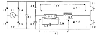
従来は図3に示す通り、放電灯(51)とそれに直列のバラスト用インダクタ(52)より構成される点灯回路(50)に流れる電流は、回路の振動周期が固定であるため、スイッチング素子(21)導通期間の電流(131)の立ち上がりとスイッチング素子(21)の遮断時におけるフライホイールダイオード(42)導通期間の電流(142)の立ち上がりは同一であった。すなわち、インバータ回路1周期の放電灯(51)に流れる電流収束時の立下りと再点り瓜時の立ち上がりが同一であり、また、インバータの発振周期を変えることはインバータ出力が変化してしまうため、放電灯(50)の電流の立下りのみを急峻にすることは不可能である。
【0003】
【発明が解決しようとする課題】
インバータの発振周期を変えずに放電灯の放電電流の立下りを急峻、かつ立ち上がりを緩慢にし、電極から放出される電子ができるだけ不活性状態とならないように配慮するとともに、再点弧時の電極損失を軽減し、放電灯の長寿命化を図る。
【0004】
【課題を解決するための手段】
ハーフブリッジ形のインバ・ータ回路を構成する少なくとも2個のコンデンサ(30・31.32)を備え、放電灯(51)と直列のバラスト用インダクタ(52)より形成される点灯回路(50)を備えた点灯装置において、前記コンデンサ(30・31・32)・点灯回路(50)によって形成される固有振動周期が前記各スイッチング素子(21・22)の通電時に大きく前記フライホイールダイオード(41・42)の通電時に小さくなるように回路構成する。
【0005】
【発明の実施の形態】
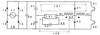
図1を用いて本発明の実施形態について説明する。本回路はハーフブリッジ形のインバータ回路を構成するコンデンサ30・31・32を備え、前記インバータ回路の高周波電圧を受ける点灯回路50を備え、前記点灯回路50は放電灯51とN1,N2二つの巻線を備えたバラスト用インダクタ52を具備し、前記バラスト用インダクタ52のN1側に放電灯51を接続し、交互にオンオフする順直列−一対のスイッチング素子21・22を備え、バラスト用インダクタ52のN2巻線を介して前記各スイッチング素子21・22と逆並列に接続するフライホイールダイオード41・42を備えている。
スイッチング素子21の導通時には放電灯51に流れる電流は131に示す経路で流れる。この回路の固有振動周期はバラスト用インダクタ52のN1、N2を含めたインダクタンスとコンデンサ31の容量により決定される。さらに、スイッチング素子21が遮断した直後はバラスト用インダクタ52に流れる電流は放電灯51、コンデンサ32を介してフライホイールダイオード42へと142に示す経路で流れる。
【0006】
フライホイールダイオード42はバラスト用インダクタンス、52のN1とN2の中間に接続されているため、この時の回路の固有振動周期はバラスト用インダクタ52のN1のインダクタンスとコンデンサ31の容量により決定され、この振動周期は、スイッチング素子21の導通時に放電灯51に流れる際の回路の固有振動周期よりバラスト用インダクタ52N2のインダクタンス分だけ小さくなっている。すなわち、放電灯51の電流が極大となるまでは振動周期が長く、電流が極大となった後は振動周期が短くなっている。したがって、放電灯に供給する電流の立ち上がりは緩慢、かつ立下りは急峻となり、電極から放出される電子ができるだけ不活性状態とならないようできるため、再点り瓜時の電極損失を軽減することができる。
【0007】
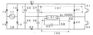
図2に他の実施例を示す。ハーフブリッジ形のインバータ回路を構成するコンデンサ37・38を備え、バラスト用インダクタ52と放電灯51からなる点灯回路50を備え、交互にオンオフする順直列一対のスイッチング素子21・22を備え、前記各スイッチング素子21・22と逆並列に接続するフライホイールダイオード41・42を備えている。さらに、前記コンデンサ37・38にダイオード61・62を介して並列接続されるコンデンサ35・36を備えている。スイッチング素子21の導適時には放電灯51に流れる電流は131に示す経路で流れる。このきはスイッチング素子21を介して点灯回路50に印加される電流はコンデンサ37およびコンデンサ35より供給される。この固有振動周期はバラスト用インダクタ52のインダクタンスおよびコンデンサ35とコンデンサ37の合計容量により決定される。さらに、スイッチング素子21が遮断した直後はバラスト用インダクタ52に流れる電流は放電灯51、コンデンサ38を介してフライホイールダイオード42へと142に示す経路で流れる。この時の回路の固有振動周期はバラスト用インダクタ52のインダクタンスとコンデンサ38の容量により決定される。この振動周期は、スイッチング素子21の導通時に放電灯51に流れる際の振動周期よりダイオード62によって逆阻止されるコンデンサ36の容量分だけ小さくなっている。すなわち、放電灯51の電流が極大となるまでは振動周期が長く、電流が極大となった後は振動周期が短くなる。
【0007】
【発明の効果】
本発明によれば、放電灯の放電電流の立下りを急峻かつ立ち上がりを緩慢にし、電極から放出される電子ができるだけ不活性状態とならないようにできるので、再点狐時の電極損失を軽減し、放電灯を長寿命とすることができる。
【図面の簡単な説明】
【図1】本発明装置の回路図である。
【図2】本発明装置の別の回路図である。
【図3】従来例装置の回路図である。
【符号の説明】
21・22:スイッチング素子
41・42:フライホイールダイオード
30・31・32:コンデンサ
50:点灯回路
35・36・37・38:コンデンサ
61・62:ダイオード[0001]
TECHNICAL FIELD OF THE INVENTION
The present invention relates to an inverter device that takes into account a longer life of a discharge lamp.
[0002]
[Prior art]
If the fall of the discharge lamp (50) at the time of current convergence is slow, electrons emitted from the electrodes of the discharge lamp (50) fall into an inactive state, and a large loss is added to the electrodes at the time of re-ignition. ), Resulting in a short life. In order to prolong the life of the discharge lamp (50), it is desirable to make the fall time when the discharge current converges steep.
Conventionally, as shown in FIG. 3, a current flowing through a lighting circuit (50) including a discharge lamp (51) and a ballast inductor (52) in series with the discharge lamp (51) has a fixed oscillation cycle of the circuit. 21) The rise of the current (131) during the conduction period and the rise of the current (142) during the conduction period of the flywheel diode (42) when the switching element (21) is cut off were the same. That is, the fall of the current flowing through the discharge lamp (51) in one cycle of the inverter circuit is the same as the fall when the current converges, and the rise when re-starting. The change in the oscillation cycle of the inverter changes the inverter output. Therefore, it is impossible to make only the fall of the current of the discharge lamp (50) steep.
[0003]
[Problems to be solved by the invention]
Without changing the oscillation cycle of the inverter, the discharge current of the discharge lamp should have a sharp fall and a slow rise, so that the electrons emitted from the electrode should be kept in an inactive state as much as possible. Reduce the loss and extend the life of the discharge lamp.
[0004]
[Means for Solving the Problems]
A lighting circuit (50) comprising at least two capacitors (30, 31.32) constituting a half-bridge type inverter circuit and formed of a ballast inductor (52) in series with a discharge lamp (51). The natural oscillation period formed by the capacitor (30, 31, 32) and the lighting circuit (50) is large when the switching elements (21, 22) are energized, and the flywheel diode (41, The circuit is configured to be small at the time of energization of 42).
[0005]
BEST MODE FOR CARRYING OUT THE INVENTION
An embodiment of the present invention will be described with reference to FIG. The circuit includes capacitors 30, 31, and 32 constituting a half-bridge type inverter circuit, and includes a lighting circuit 50 for receiving a high-frequency voltage of the inverter circuit. The lighting circuit 50 includes a discharge lamp 51 and two windings N1 and N2. A ballast inductor 52 having a wire, a discharge lamp 51 is connected to the N1 side of the ballast inductor 52, and a series connection-a pair of switching elements 21 and 22 that are turned on and off alternately is provided. Flywheel diodes 41 and 42 are connected in anti-parallel with the switching elements 21 and 22 via an N2 winding.
When the switching element 21 is turned on, the current flowing through the discharge lamp 51 flows through a path indicated by 131. The natural oscillation period of this circuit is determined by the inductance of the ballast inductor 52 including N1 and N2 and the capacitance of the capacitor 31. Further, immediately after the switching element 21 is cut off, the current flowing through the ballast inductor 52 flows through the discharge lamp 51 and the capacitor 32 to the flywheel diode 42 via the path indicated by 142.
[0006]
Since the flywheel diode 42 is connected between the ballast inductance 52 and N1 and N2 of the ballast inductance 52, the natural oscillation cycle of the circuit at this time is determined by the inductance N1 of the ballast inductor 52 and the capacitance of the capacitor 31. The oscillation cycle is smaller than the natural oscillation cycle of the circuit when flowing through the discharge lamp 51 when the switching element 21 is conducting by the inductance of the ballast inductor 52N2. That is, the oscillation cycle is long until the current of the discharge lamp 51 reaches a maximum, and the oscillation cycle decreases after the current reaches a maximum. Therefore, the rise of the current supplied to the discharge lamp is slow, and the fall is steep, so that the electrons emitted from the electrode can be kept in an inactive state as much as possible. it can.
[0007]
FIG. 2 shows another embodiment. It includes capacitors 37 and 38 that constitute a half-bridge type inverter circuit, includes a lighting circuit 50 including a ballast inductor 52 and a discharge lamp 51, and includes a pair of switching elements 21 and 22 that are turned on and off alternately. It has flywheel diodes 41 and 42 connected in antiparallel with the switching elements 21 and 22. Furthermore, capacitors 35 and 36 are connected in parallel to the capacitors 37 and 38 via diodes 61 and 62. When the switching element 21 is properly applied, the current flowing through the discharge lamp 51 flows through a path indicated by 131. In this case, the current applied to the lighting circuit 50 via the switching element 21 is supplied from the capacitors 37 and 35. The natural oscillation period is determined by the inductance of the ballast inductor 52 and the total capacitance of the capacitors 35 and 37. Further, immediately after the switching element 21 is cut off, the current flowing through the ballast inductor 52 flows through the discharge lamp 51 and the capacitor 38 to the flywheel diode 42 via the path indicated by 142. The natural oscillation period of the circuit at this time is determined by the inductance of the ballast inductor 52 and the capacitance of the capacitor 38. This oscillation period is smaller than the oscillation period when the switching element 21 conducts and flows through the discharge lamp 51 by the capacitance of the capacitor 36 that is reversely blocked by the diode 62. In other words, the oscillation cycle is long until the current of the discharge lamp 51 becomes maximum, and becomes short after the current becomes maximum.
[0007]
【The invention's effect】
According to the present invention, the fall of the discharge current of the discharge lamp is made sharp and the rise is made slow so that the electrons emitted from the electrodes can be kept in an inactive state as much as possible. In addition, the life of the discharge lamp can be increased.
[Brief description of the drawings]
FIG. 1 is a circuit diagram of the device of the present invention.
FIG. 2 is another circuit diagram of the device of the present invention.
FIG. 3 is a circuit diagram of a conventional device.
[Explanation of symbols]
21/22: Switching element 41/42: Flywheel diode 30, 31/32: Capacitor 50: Lighting circuit 35/36/37/38: Capacitor 61/62: Diode