JP2004268342A - Image formation device - Google Patents
Image formation device Download PDFInfo
- Publication number
- JP2004268342A JP2004268342A JP2003060432A JP2003060432A JP2004268342A JP 2004268342 A JP2004268342 A JP 2004268342A JP 2003060432 A JP2003060432 A JP 2003060432A JP 2003060432 A JP2003060432 A JP 2003060432A JP 2004268342 A JP2004268342 A JP 2004268342A
- Authority
- JP
- Japan
- Prior art keywords
- voltage
- unit
- power
- image forming
- power supply
- Prior art date
- Legal status (The legal status is an assumption and is not a legal conclusion. Google has not performed a legal analysis and makes no representation as to the accuracy of the status listed.)
- Pending
Links
Images


Landscapes
- Control Or Security For Electrophotography (AREA)
- Accessory Devices And Overall Control Thereof (AREA)
Abstract
Description
【0001】
【発明の属する技術分野】
本発明は、コピー、FAX(facsimile)、プリンタ等の電子写真を利用した画像形成装置に関する。
【0002】
【従来の技術】
従来、省電力化を実現するための機能を備えた画像形成装置として、印字処理中の駆動モードから印字処理を停止した状態の省電力モードに移行した際、レーザ発光部の駆動電源、帯電、現像、及び転写用の高圧電源、感光体ドラム、定着部、用紙搬送系などの駆動電源への電源電流をオフにすることにより、消費電力の低減を図るものが知られている。また、画像形成装置には、印字途中で装置本体の開閉カバーを開いたときに、ユーザの安全を図るために駆動部への電源供給を遮断するインターロックスイッチが設けられている。
【0003】
図5は従来の画像形成装置の電源供給回路の構成を示す図である。
【0004】
図5において、スイッチング電源1は、AC100V電源から供給される交流電圧を整流化するブリッジダイオード20、トランス21、ダイオード22a,b、負荷抵抗7,8を有し、24V電圧及び5V電圧を生成する。スイッチング電源1において、24V電圧供給側は、インターロックスイッチ4及び電力遮断スイッチ5を介して駆動負荷部2に電圧を供給し、5V電圧供給側はマイコン回路部3及びロジック回路部9に電圧を供給する。また、24V電圧供給側は負荷抵抗7を介してグラウンドに接続され、5V電圧供給側は負荷抵抗8を介してグラウンドに接続されている。
【0005】
駆動負荷部2は、スキャナ部31、給紙カセット及び給紙ローラ等を有する用紙搬送部32、及び感光体ドラム、現像装置、定着装置等を有する画像形成部33を含む。ロジック回路部9は、駆動負荷部2による画像形成処理に必要な制御IC(Integrated Curcuit)等の電気部品における論理回路である。
【0006】
画像形成装置本体に取り付けられたカバー(図示省略)が開状態の時、インターロックスイッチ4はオフとなり駆動負荷部2との通電を遮断し、カバーが閉状態の時は、インターロックスイッチ4はオンとなり駆動負荷部2への電圧供給が行われる。カバー開閉検知センサ6は、直列接続される2つの抵抗を有し、インターロックスイッチ4のオン、オフの切り替えにより、スイッチング電源1からマイコン回路部3への電圧の供給及び遮断の切り替えを行う。マイコン回路部3はカバー開閉検知センサ6からの供給電圧の有無により、インターロックスイッチ4のオンオフ状態を検知することができる。マイコン回路部3は、駆動モードでは電力遮断スイッチ5に電圧を印加し、省電力モード時には電力遮断スイッチ5への電圧供給を遮断することにより、駆動負荷部2へ電圧供給及び遮断を制御する。
【0007】
スイッチング電源1では、パワーオン時の2次側電圧(24V、5V)のスムーズな立ち上げを行う目的と、低負荷もしくは無負荷状態においても電圧を所定範囲内で一定に保つため、一定電流を負荷抵抗7,8に消費させている。例えば、省電力モード時に電力遮断スイッチ5への電圧供給がオフとなり、またはカバーが開状態となることでインターロックスイッチ4が開状態となった場合は、24V電圧供給側が無負荷状態となり、5V電圧供給側が有負荷状態になるため、電源のクロスレギュレーションの関係で、24V電圧供給側から供給される電圧が24V以上に上昇する。この電圧上昇を所定値以内に抑えるために、24V電圧供給側から供給される電流が負荷抵抗7を介してグラウンドに流れるように制御している。
【0008】
【発明が解決しようとする課題】
つまり、省電力モード時またはカバーが開状態である時は、24V電圧供給側から無駄にグラウンドに流す電流が多くなり、電力使用効率の悪化及びそれに伴う消費電力の悪化を招くという問題点があった。
【0009】
本発明は上記問題点を解決するためになされたものであり、省電力モード時またはカバーが開状態である時の電力使用効率の改善を図り、消費電力の低減を図ることが可能な画像形成装置を提供することが目的である。
【0010】
【課題を解決するための手段】
本発明の請求項1に係る画像形成装置は、画像形成処理を行うための駆動手段と、前記駆動手段による画像形成処理を制御する制御手段と、前記駆動手段に第1の電圧を供給すると共に前記制御手段に第2の電圧を供給する電源と、前記電源から前記駆動手段に供給される第1の電圧を遮断する遮断手段と、前記遮断手段により前記電源から前記駆動手段に供給される第1の電圧が遮断された場合、第1の電圧を蓄電する蓄電手段と、前記蓄電手段に所定値以上の電圧が蓄電された場合に、前記制御手段への電圧供給源を前記電源から前記蓄電手段に切り替える切り替え手段とを備えた構成としたので、前記駆動手段による画像形成処理が停止している時、負荷抵抗の代わりに前記蓄電手段を用いてクロスレギュレーションによる第1の電圧の昇圧を抑制すると共に第1の電圧の蓄電を行うことができ、装置全体としての電力使用効率の改善を図り、消費電力の低減を図ることができる。
【0011】
本発明の請求項2に係る画像形成装置は、請求項1に記載される画像形成装置において、前記切り替え手段は、前記制御手段に前記蓄電手段から第2の電圧が供給され、前記蓄電手段による前記制御手段への第2の電圧供給中に、前記蓄電手段に蓄電される電圧の値が所定値未満になった場合は、前記制御手段への電圧供給源を前記蓄電手段から前記電源に切り替える構成としたので、前記制御手段への供給電圧を一定に保つことができる。
【0012】
本発明の請求項3に係る画像形成装置は、請求項1に記載される画像形成装置において、前記遮断手段は、前記駆動手段による画像形成処理が休止している省電力モード時に、前記駆動手段に供給される第1の電圧を遮断する構成としたので、省電力モード時に、負荷抵抗の代わりに前記蓄電手段を用いてクロスレギュレーションを防止すると共に第1の電圧の蓄電を行うことができ、装置全体としての電力使用効率の改善を図り、消費電力の低減を図ることができる。
【0013】
本発明の請求項4に係る画像形成装置は、請求項1に記載される画像形成装置において、装置本体を覆う開閉可能なカバーを備え、前記遮断手段は、前記カバーに連動し、前記カバーが開状態である場合に前記駆動手段に供給される第1の電圧を遮断するインターロックスイッチであるので、前記カバーが開状態である時に、負荷抵抗の代わりに前記蓄電手段を用いてクロスレギュレーションを防止すると共に第1の電圧の蓄電を行うことができ、装置全体としての電力使用効率の改善を図り、消費電力の低減を図ることができる。
【0014】
【発明の実施の形態】
以下、本発明による画像形成装置の一例として本発明の一実施の形態によるデジタル複合機について図面を参照しながら説明する。図1は、本発明の一実施の形態によるデジタル複合機の機械的構成を主に示す側面概略図である。
【0015】
デジタル複合機1は、本体部200と、本体部200の左側に配設された用紙後処理部300と、ユーザが種々の操作指令等を入力するための操作部400と、本体部200の上部に配設された原稿読み取り部500と、原稿読み取り部500の上方に配設された原稿給送部600とから構成される。
【0016】
操作部400は、タッチパネル401、スタートキー402及びテンキー403等を備える。タッチパネル401は、種々の操作画面を表示するとともに、ユーザが種々の操作指令を入力するための種々の操作ボタン等を表示する。スタートキー402は、ユーザが印刷実行指令等を入力するために用いられ、テンキー403は、印刷枚数等を入力するために用いられる。
【0017】
原稿給送部600は、原稿収納部601、原稿排出部602、給紙ローラ603及び原稿搬送部604等を備え、原稿読み取り部500は、スキャナ501等を備える。給紙ローラ603は、原稿収納部601にセットされた原稿を繰り出し、原稿搬送部604は、繰り出される原稿を1枚ずつ順にスキャナ501上に搬送する。スキャナ501は搬送される原稿を順次読み取り、読み取られた原稿は原稿排出部602に排出される。
【0018】
本体部200は、複数の給紙カセット201、複数の給紙ローラ202、転写ローラ203、感光体ドラム204、露光装置206、現像装置207、定着ローラ208、排出口209、及び排出トレイ210等を備える。
【0019】
感光体ドラム204は、矢印方向に回転しながら帯電装置(図示省略)によって一様に帯電される。露光装置206は、原稿読み取り部500において読み取られた原稿の画像データに基づいて生成された変調信号をレーザ光に変換して出力し、感光体ドラム204に静電潜像を形成する。現像装置207は、黒色の現像剤を感光体ドラム204に供給してトナー画像を形成する。
【0020】
一方、給紙ローラ202は、印刷用紙が収納された給紙カセット201から印刷用紙を引き出し、転写ローラ203まで給送する。転写ローラ203は、搬送された印刷用紙に感光体ドラム204上のトナー像を転写させ、定着ローラ208は、転写されたトナー像を加熱して印刷用紙に定着させる。その後、印刷用紙は、本体部200の排出口209から用紙後処理部300に搬入される。また、印刷用紙は、必要に応じて排出トレイ210へも排出される。
【0021】
用紙後処理部300は、搬入口301、印刷用紙搬送部302、搬出口303及びスタックトレイ304等を備える。印刷用紙搬送部302は、排出口209から搬入口301に搬入された印刷用紙を順次搬送し、最終的に搬出口303からスタックトレイ304へ印刷用紙を排出する。スタックトレイ304は、搬出口303から搬出された印刷用紙の集積枚数に応じて矢印方向に上下動可能に構成されている。
【0022】
図2は図1に示すデジタル複合機の外観の概略を示した斜視図である。
【0023】
デジタル複合機100において、本体部200前面に開閉自在に取り付けられた扉カバー103を備える。インターロックスイッチ(遮断手段)4は、例えば突起部を備えた押しボタンスイッチであり、カバー103が閉状態のときはカバー103によってその突起部が押し込まれてオンになり、カバー103が開状態の時は、インターロックスイッチ4がオフになり、スキャナ501におけるレーザ発光部(図示せず)、現像装置207、転写ローラ203、定着ローラ208等の駆動負荷部2への電圧供給が遮断される。なお、本実施の形態では、カバー103の開閉に連動するインターロックスイッチ4について説明しているが、装置本体部200に内蔵される現像装置207、感光体ドラム204等の着脱により、駆動電源への電圧供給を遮断するインターロックスイッチ(図示省略)、給紙トレイ201のスライドにより駆動電源への電圧供給を遮断するインターロックスイッチ(図示省略)についても本発明は適用可能である。
【0024】
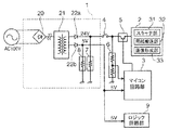
図3は図1に示すデジタル複合機の電源供給回路の構成を示す図である。
【0025】
図において、スイッチング電源1は、AC100V電源から供給される交流電圧を整流化するブリッジダイオード20、トランス21、ダイオード22a,b、負荷抵抗7,8を有し、24V電圧及び5V電圧を生成する。スイッチング電源1において、24V電圧供給側は、インターロックスイッチ4及び電力遮断スイッチ5を介して駆動負荷部2に電圧を供給し、5V電圧供給側はマイコン回路部3及びロジック回路部9に電圧を供給する。また、24V電圧供給側は負荷抵抗7及び負荷経路スイッチ11を介してグラウンドに接続され、5V電圧供給側は負荷抵抗8を介してグラウンドに接続されている。
【0026】
駆動負荷部(駆動手段)2は、スキャナ部31、用紙搬送部32、及び画像形成部33を含む。スキャナ部31は、図1に示すスキャナ501等から構成され、用紙搬送部32は、図1に示す給紙カセット201及び給紙ローラ202等から構成され、画像形成部33は、図1に示す露光装置206、現像装置207、転写ローラ203、定着ローラ208等から構成され、24V電圧供給側からの電圧供給により各部が作動し、給紙ローラ202は印刷用紙を画像形成部33へ搬送し、現像装置207はスキャナ501により読み取られた画像データに対応するトナー像を形成し、転写ローラ203はトナー像を印刷用紙に転写し、定着ローラ208はトナー像を印刷用紙に定着させて画像を形成する。ロジック回路部(制御手段)9は、駆動負荷部2による画像形成処理に必要な制御IC(Integrated Curcuit)等の電気部品における論理回路である。
【0027】
デジタル複合機本体部200に取り付けられたカバー103が開かれた状態の時は、インターロックスイッチ4はオフとなり駆動負荷部2との通電を遮断し、カバーが閉状態の時は、インターロックスイッチ4はオンとなり駆動負荷部2への電源供給が行われる。カバー開閉検知センサ6は、直列接続される2つの抵抗を有し、インターロックスイッチ4のオン、オフの切り替えにより、スイッチング電源1からマイコン回路部3への電圧の供給及び遮断の切り替えを行う。マイコン回路部3はカバー開閉検知センサ6からの供給電圧の有無により、インターロックスイッチ4のオンオフ状態を検知することができる。
【0028】
マイコン回路部3は、デジタル複合機の制御プログラムを記憶するROM(Read Only Memory)、一時的にデータを保管するRAM(Random Access Memory)、及びマイクロコンピュータ等からなり、各部の動作を制御する。マイコン回路部3は、装置本体の動作モードを管理し、印刷動作中である駆動モード時には電力遮断スイッチ(遮断手段)5に電圧を印加することにより、駆動負荷部2への電圧供給を行い、印刷動作を休止している省電力モード時には、電力遮断スイッチ5への電圧供給を遮断し、駆動負荷部2への電圧供給を停止する。ここで、駆動モードについては操作部400によりユーザからの操作指示を受け付け、駆動負荷部2により印刷処理が行われている状態であり、また省電力モードには駆動負荷部2の休止状態が一定期間経過した状態をいう。
【0029】
蓄電装置12は蓄電スイッチ10を介してスイッチング電源1に接続され、蓄電スイッチ10がオンになると、24V電圧供給側からの供給電圧を蓄電する。ロジック回路部9は電源供給スイッチ13を介して5V電圧供給側に接続されると共に、電源供給スイッチ14を介して蓄電装置12に接続される。電源供給スイッチ13は5V電圧供給側からロジック回路部9への電圧の供給及び遮断を制御するためのスイッチング素子であり、電源供給スイッチ14は蓄電装置12からロジック回路部9への電圧の供給及び遮断を制御するためのスイッチング素子である。
【0030】
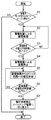
本発明の画像形成装置の動作について図3及び図4を用いて説明する。図4は図3に示す電源供給回路の動作を説明するためのフローチャートである。
【0031】
ステップS1において、マイコン回路部3は、インターロックスイッチ4が開状態または電力遮断スイッチ5がオフであり、駆動負荷部2が低負荷または無負荷状態であるか否かを判断する。駆動負荷部2が低負荷または無負荷状態である場合は、負荷経路スイッチ11をオフにし、24V電圧供給側から負荷抵抗7を介してグラウンドに流れる電流経路を断ち、蓄電スイッチ10をオンにし、24V電圧供給側から蓄電装置12に電圧が供給されるようにする(ステップS2)。
【0032】
次いで、蓄電装置12に蓄電される電圧をモニターし、電圧が5V以上蓄電されたか否かを判断し(ステップS3)、蓄電装置12に5V以上の電圧が蓄電されたことを検知した場合、蓄電スイッチ10をオフにし、蓄電装置12による蓄電処理を停止し、同時に負荷経路スイッチ11をオンにし、24V電圧供給側の負荷経路をグラウンド側に切り替える (ステップS4)。そして、電源供給スイッチ13をオフにし、かつ、電源供給スイッチ14をオンにすることで、ロジック回路部9への電圧供給源を5V電圧供給側から蓄電装置12に切り替える(ステップS5)。
【0033】
更に、蓄電装置12に蓄電される電圧をモニターし、電圧が所定値(4.75V)未満になったか否かを判断し(ステップS6)、電圧が所定値未満になったことを検知した場合、電源供給スイッチ13をオンにすると同時に電源供給スイッチ14をオフにし、ロジック回路部9への電圧供給源を蓄電装置12からスイッチング電源1の5V電圧供給側に戻す(ステップS7)。
【0034】
このように構成された電源供給回路を有するデジタル複合機100によれば、省電力モード時またはインターロックスイッチ4が開状態であり、駆動負荷部2が無負荷状態である場合、クロスレギュレーションによる24V電圧の過昇圧を防ぐため、24V電圧供給側からの供給電圧を蓄電装置12に蓄電させ、さらに、蓄電装置12に5V電圧が蓄電された時に、蓄電装置12に蓄電された電圧をロジック回路部9に供給するので、装置全体としての電力使用効率の改善を図り、消費電力の低減を図ることができる。また、蓄電装置12に蓄電される電圧が所定値未満になった場合は、前記ロジック回路部9への電圧供給源を前記蓄電装置12からスイッチング電源1に切り替えるので、前記ロジック回路部9への供給電圧を一定に保つことができる。
【0035】
【発明の効果】
このように、本発明によれば、省電力モード時または装置本体のカバーが開状態である時の電力使用効率の改善を図り、消費電力の低減を図ることができる。
【図面の簡単な説明】
【図1】本発明の一実施の形態によるデジタル複合機の機械的構成を主に示す側面概略図である。
【図2】図1に示すデジタル複合機の外観の概略を示した斜視図である。
【図3】図1に示すデジタル複合機の電源供給回路の構成を示す図である。
【図4】図3に示す電源供給回路の動作を説明するためのフローチャートである。
【図5】従来の画像形成装置の電源供給回路の構成を示す図である。
【符号の説明】
100 デジタル複合機
1 スイッチング電源
2 駆動負荷部
3 マイコン回路部
4 インターロックスイッチ
5 電力遮断スイッチ
6 カバー開閉検知センサ
7,8負荷抵抗
9 ロジック回路部
10 蓄電スイッチ
11 負荷経路スイッチ
12 蓄電装置
13、14 電源供給スイッチ[0001]
TECHNICAL FIELD OF THE INVENTION
The present invention relates to an image forming apparatus using electrophotography, such as a copy, a facsimile (FAX), and a printer.
[0002]
[Prior art]
Conventionally, as an image forming apparatus having a function for realizing power saving, when shifting from the driving mode during the printing process to the power saving mode in a state where the printing process is stopped, the driving power source of the laser emitting unit, charging, It is known to reduce power consumption by turning off a power supply current to a driving power supply for a high-voltage power supply for development and transfer, a photosensitive drum, a fixing unit, a paper transport system, and the like. In addition, the image forming apparatus is provided with an interlock switch that shuts off power supply to the drive unit in order to ensure user safety when the opening / closing cover of the apparatus main body is opened during printing.
[0003]
FIG. 5 is a diagram showing a configuration of a power supply circuit of a conventional image forming apparatus.
[0004]
In FIG. 5, the
[0005]
The
[0006]
When a cover (not shown) attached to the image forming apparatus main body is in an open state, the
[0007]
In the
[0008]
[Problems to be solved by the invention]
In other words, in the power saving mode or when the cover is open, a large amount of current flows from the 24 V voltage supply side to the ground unnecessarily, which causes a problem that the power use efficiency and the power consumption are reduced. Was.
[0009]
The present invention has been made in order to solve the above-described problems, and has been made to improve the power use efficiency in the power saving mode or when the cover is open, and to reduce the power consumption. The purpose is to provide a device.
[0010]
[Means for Solving the Problems]
An image forming apparatus according to
[0011]
An image forming apparatus according to a second aspect of the present invention is the image forming apparatus according to the first aspect, wherein the switching unit is configured to supply a second voltage from the power storage unit to the control unit, If the value of the voltage stored in the power storage unit becomes smaller than a predetermined value during the supply of the second voltage to the control unit, a voltage supply source to the control unit is switched from the power storage unit to the power supply. With this configuration, the supply voltage to the control unit can be kept constant.
[0012]
An image forming apparatus according to a third aspect of the present invention is the image forming apparatus according to the first aspect, wherein the blocking unit is configured to control the driving unit in a power saving mode in which image forming processing by the driving unit is suspended. Is configured to cut off the first voltage supplied to the power supply mode, so that in the power saving mode, the first voltage can be stored while preventing the cross regulation by using the power storage unit instead of the load resistance, The power use efficiency of the entire apparatus can be improved, and the power consumption can be reduced.
[0013]
An image forming apparatus according to a fourth aspect of the present invention is the image forming apparatus according to the first aspect, further comprising an openable / closable cover that covers the apparatus main body, wherein the blocking unit is interlocked with the cover, and the cover is Since the interlock switch cuts off the first voltage supplied to the driving means when the cover is in the open state, when the cover is in the open state, cross regulation is performed using the power storage means instead of the load resistance. Thus, the first voltage can be stored, and the power use efficiency of the entire apparatus can be improved, and the power consumption can be reduced.
[0014]
BEST MODE FOR CARRYING OUT THE INVENTION
Hereinafter, a digital multifunction peripheral according to an embodiment of the present invention will be described as an example of an image forming apparatus according to the present invention with reference to the drawings. FIG. 1 is a schematic side view mainly showing a mechanical configuration of a digital multifunction peripheral according to an embodiment of the present invention.
[0015]
The digital multifunction peripheral 1 includes a
[0016]
The
[0017]
The
[0018]
The
[0019]
The
[0020]
On the other hand, the
[0021]
The
[0022]
FIG. 2 is a perspective view schematically showing the appearance of the digital multifunction peripheral shown in FIG.
[0023]
The digital multifunction peripheral 100 includes a
[0024]
FIG. 3 is a diagram showing a configuration of a power supply circuit of the digital multifunction peripheral shown in FIG.
[0025]
In the figure, a switching
[0026]
The drive load unit (drive unit) 2 includes a
[0027]
When the
[0028]
The
[0029]
The
[0030]
The operation of the image forming apparatus of the present invention will be described with reference to FIGS. FIG. 4 is a flowchart for explaining the operation of the power supply circuit shown in FIG.
[0031]
In step S1, the
[0032]
Next, the voltage stored in the
[0033]
Further, the voltage stored in the
[0034]
According to the digital multifunction peripheral 100 having the power supply circuit configured as described above, in the power saving mode or when the
[0035]
【The invention's effect】
As described above, according to the present invention, it is possible to improve the power use efficiency in the power saving mode or when the cover of the apparatus main body is in the open state, and to reduce the power consumption.
[Brief description of the drawings]
FIG. 1 is a schematic side view mainly showing a mechanical configuration of a digital multifunction peripheral according to an embodiment of the present invention.
FIG. 2 is a perspective view schematically showing an appearance of the digital multifunction peripheral shown in FIG.
FIG. 3 is a diagram illustrating a configuration of a power supply circuit of the digital multifunction peripheral illustrated in FIG. 1;
FIG. 4 is a flowchart for explaining an operation of the power supply circuit shown in FIG. 3;
FIG. 5 is a diagram illustrating a configuration of a power supply circuit of a conventional image forming apparatus.
[Explanation of symbols]
REFERENCE SIGNS
Claims (4)
前記駆動手段による画像形成処理を制御する制御手段と、
前記駆動手段に第1の電圧を供給すると共に前記制御手段に第2の電圧を供給する電源と、
前記電源から前記駆動手段に供給される第1の電圧を遮断する遮断手段と、
前記遮断手段により前記電源から前記駆動手段に供給される第1の電圧が遮断された場合、第1の電圧を蓄電する蓄電手段と、
前記蓄電手段に所定値以上の電圧が蓄電された場合に、前記制御手段への電圧供給源を前記電源から前記蓄電手段に切り替える切り替え手段とを備えたことを特徴とする画像形成装置。Driving means for performing image forming processing;
Control means for controlling an image forming process by the driving means,
A power supply that supplies a first voltage to the driving means and supplies a second voltage to the control means;
Blocking means for blocking a first voltage supplied from the power supply to the driving means;
Power storage means for storing the first voltage when the first voltage supplied from the power supply to the drive means is cut off by the cutoff means;
An image forming apparatus comprising: a switching unit that switches a voltage supply source to the control unit from the power supply to the power storage unit when a voltage equal to or higher than a predetermined value is stored in the power storage unit.
前記切り替え手段は、
前記制御手段に前記蓄電手段から第2の電圧が供給され、前記蓄電手段による前記制御手段への第2の電圧供給中に、前記蓄電手段に蓄電される電圧の値が所定値未満になった場合は、前記制御手段への電圧供給源を前記蓄電手段から前記電源に切り替えることを特徴とする画像形成装置。The image forming apparatus according to claim 1,
The switching means,
A second voltage is supplied from the power storage unit to the control unit, and a value of a voltage stored in the power storage unit becomes less than a predetermined value while the power storage unit supplies the second voltage to the control unit. In this case, an image forming apparatus switches a voltage supply source to the control unit from the power storage unit to the power supply.
前記遮断手段は、前記駆動手段による画像形成処理が休止している省電力モード時に、前記駆動手段に供給される第1の電圧を遮断することを特徴とする画像形成装置。The image forming apparatus according to claim 1,
The image forming apparatus according to claim 1, wherein the interrupting unit interrupts the first voltage supplied to the driving unit in a power saving mode in which the image forming process by the driving unit is suspended.
装置本体を覆う開閉可能なカバーを備え、
前記遮断手段は、前記カバーに連動し、前記カバーが開状態である場合に前記駆動手段に供給される第1の電圧を遮断するインターロックスイッチであることを特徴とする画像形成装置。The image forming apparatus according to claim 1,
Equipped with an openable / closable cover that covers the device body,
The image forming apparatus according to claim 1, wherein the interrupting unit is an interlock switch that interlocks with the cover and shuts off a first voltage supplied to the driving unit when the cover is open.
Priority Applications (1)
| Application Number | Priority Date | Filing Date | Title |
|---|---|---|---|
| JP2003060432A JP2004268342A (en) | 2003-03-06 | 2003-03-06 | Image formation device |
Applications Claiming Priority (1)
| Application Number | Priority Date | Filing Date | Title |
|---|---|---|---|
| JP2003060432A JP2004268342A (en) | 2003-03-06 | 2003-03-06 | Image formation device |
Publications (1)
| Publication Number | Publication Date |
|---|---|
| JP2004268342A true JP2004268342A (en) | 2004-09-30 |
Family
ID=33122976
Family Applications (1)
| Application Number | Title | Priority Date | Filing Date |
|---|---|---|---|
| JP2003060432A Pending JP2004268342A (en) | 2003-03-06 | 2003-03-06 | Image formation device |
Country Status (1)
| Country | Link |
|---|---|
| JP (1) | JP2004268342A (en) |
Cited By (3)
| Publication number | Priority date | Publication date | Assignee | Title |
|---|---|---|---|---|
| JP2007322372A (en) * | 2006-06-05 | 2007-12-13 | Yokogawa Electric Corp | Ic tester |
| JP2012020573A (en) * | 2010-06-18 | 2012-02-02 | Canon Inc | Electronic device and image forming apparatus |
| JP2013097035A (en) * | 2011-10-28 | 2013-05-20 | Kyocera Document Solutions Inc | Electrical equipment, and image forming apparatus including the same |
-
2003
- 2003-03-06 JP JP2003060432A patent/JP2004268342A/en active Pending
Cited By (3)
| Publication number | Priority date | Publication date | Assignee | Title |
|---|---|---|---|---|
| JP2007322372A (en) * | 2006-06-05 | 2007-12-13 | Yokogawa Electric Corp | Ic tester |
| JP2012020573A (en) * | 2010-06-18 | 2012-02-02 | Canon Inc | Electronic device and image forming apparatus |
| JP2013097035A (en) * | 2011-10-28 | 2013-05-20 | Kyocera Document Solutions Inc | Electrical equipment, and image forming apparatus including the same |
Similar Documents
| Publication | Publication Date | Title |
|---|---|---|
| US20070166061A1 (en) | Image forming apparatus and image forming method | |
| JP3666954B2 (en) | Copying machine and its control apparatus and method | |
| JP2005253285A (en) | Power supply controlling device, heat-generating device, fixing device, image forming apparatus, and method and program for controlling power supply | |
| JP5914287B2 (en) | Image forming apparatus and power control method | |
| JP2004115144A (en) | Image formation device, tab paper mode processing method of image formation device, computer readable recording medium, and program | |
| JP2009173425A (en) | Paper conveying device, image formation device with it, paper conveying method, paper conveying program, and computer-readable recording medium recording the program | |
| JP2004195927A (en) | Printer, method of controlling the same, program, and recording medium | |
| JP2004268342A (en) | Image formation device | |
| JPH1039562A (en) | Image forming device | |
| JP2009128705A (en) | Image forming device | |
| JP4995532B2 (en) | Heating system, image forming device | |
| JP7371485B2 (en) | Power supply device and image forming device | |
| JP2015138249A (en) | image forming apparatus | |
| JP2001109316A (en) | Image forming device | |
| JP2011063344A (en) | Image forming device | |
| JP2005141046A (en) | Image forming apparatus | |
| JP3924886B2 (en) | Copy machine | |
| JP2005250326A (en) | Image forming apparatus | |
| JPH11143188A (en) | Image forming device | |
| JP2005221772A (en) | Fixing device and image forming apparatus | |
| JP4605580B2 (en) | Image forming apparatus | |
| JPH0934317A (en) | Picture forming device and mode setting method of picture forming device | |
| JPH10148982A (en) | Image forming device | |
| JPH09197735A (en) | Image forming device | |
| JP2000289885A (en) | Sheet carrier device, picture image formation device and its control method |
Legal Events
| Date | Code | Title | Description |
|---|---|---|---|
| A621 | Written request for application examination |
Free format text: JAPANESE INTERMEDIATE CODE: A621 Effective date: 20050324 |
|
| A977 | Report on retrieval |
Free format text: JAPANESE INTERMEDIATE CODE: A971007 Effective date: 20071001 |
|
| A131 | Notification of reasons for refusal |
Free format text: JAPANESE INTERMEDIATE CODE: A131 Effective date: 20090203 |
|
| A02 | Decision of refusal |
Free format text: JAPANESE INTERMEDIATE CODE: A02 Effective date: 20090609 |