JP2004268103A - Laser beam machining method - Google Patents
Laser beam machining method Download PDFInfo
- Publication number
- JP2004268103A JP2004268103A JP2003063777A JP2003063777A JP2004268103A JP 2004268103 A JP2004268103 A JP 2004268103A JP 2003063777 A JP2003063777 A JP 2003063777A JP 2003063777 A JP2003063777 A JP 2003063777A JP 2004268103 A JP2004268103 A JP 2004268103A
- Authority
- JP
- Japan
- Prior art keywords
- workpiece
- region
- laser
- cutting
- processing
- Prior art date
- Legal status (The legal status is an assumption and is not a legal conclusion. Google has not performed a legal analysis and makes no representation as to the accuracy of the status listed.)
- Pending
Links
Images


Classifications
-
- C—CHEMISTRY; METALLURGY
- C03—GLASS; MINERAL OR SLAG WOOL
- C03B—MANUFACTURE, SHAPING, OR SUPPLEMENTARY PROCESSES
- C03B33/00—Severing cooled glass
- C03B33/02—Cutting or splitting sheet glass or ribbons; Apparatus or machines therefor
- C03B33/0222—Scoring using a focussed radiation beam, e.g. laser
Landscapes
- Chemical & Material Sciences (AREA)
- Engineering & Computer Science (AREA)
- Materials Engineering (AREA)
- Organic Chemistry (AREA)
- Processing Of Stones Or Stones Resemblance Materials (AREA)
- Laser Beam Processing (AREA)
- Dicing (AREA)
Abstract
Description
【0001】
【発明の属する技術分野】
【0002】
本発明は、半導体材料基板、圧電材料基板やガラス基板等の加工対象物の切断に使用されるレーザ加工方法に関する。
【0003】
【従来の技術】
従来におけるこの種の技術を開示する文献として、下記の特許文献1を例示することができる。この特許文献1の明細書には、レーザ光を照射することにより加工対象物の内部に切断予定ラインに沿って改質領域を形成し、この改質領域を起点として加工対象物を切断する技術が記載されている。
【0004】
【特許文献1】
国際公開第02/22301号パンフレット
【0005】
【発明が解決しようとする課題】
この特許文献1記載の技術は、加工対象物を切断予定ラインに沿って精度良く切断することのできる極めて有効な技術であるため、改質領域を起点として加工対象物をより一層確実に且つ高精度に切断する技術が望まれていた。
【0006】
そこで、本発明は、このような事情に鑑みてなされたものであり、切断予定ラインに沿って加工対象物を確実且つ高精度に切断することのできるレーザ加工方法を提供することを目的とする。
【0007】
【課題を解決するための手段】
上記目的を達成するために、本発明に係るレーザ加工方法は、拡張可能な保持部材の表面に固定されたウェハ状の加工対象物の内部に集光点を合わせてレーザ光を照射し、加工対象物の内部に改質領域を形成し、この改質領域によって、加工対象物の切断予定ラインに沿って加工対象物のレーザ光入射面から所定距離内側に切断起点領域を形成する工程と、切断起点領域を形成する工程後、加工対象物に対して吸収性を有するレーザ光を切断予定ラインに沿って加工対象物に照射することで、切断予定ラインに沿って加工対象物を切断する工程と、加工対象物を切断する工程後、保持部材を拡張させることで、切断された加工対象物のそれぞれの部分を離間させる工程とを備えることを特徴とする。
【0008】
このレーザ加工方法においては、多光子吸収により形成される改質領域によって、加工対象物を切断すべき所望の切断予定ラインに沿って加工対象物の内部に切断起点領域を形成することができる。そして、加工対象物に対して吸収性を有するレーザ光を切断予定ラインに沿って加工対象物に照射することで、切断起点領域を起点として加工対象物に割れを発生させ、切断予定ラインに沿って加工対象物を精度良く切断することができる。しかも、加工対象物が固定された保持部材を拡張させることで、加工対象物のそれぞれの部分が離間することになるため、切断予定ラインに沿った加工対象物の切断の確実性をより一層向上させることができる。
【0009】
また、本発明に係るレーザ加工方法は、拡張可能な保持部材の表面に固定されたウェハ状の加工対象物の内部に集光点を合わせてレーザ光を照射し、加工対象物の内部に改質領域を形成し、この改質領域によって、加工対象物の切断予定ラインに沿って加工対象物のレーザ光入射面から所定距離内側に切断起点領域を形成する工程と、切断起点領域を形成する工程後、加工対象物に対して吸収性を有するレーザ光を切断予定ラインに沿って加工対象物に照射する工程と、加工対象物に照射する工程後、保持部材を拡張させることで、加工対象物を切断し、かつ切断された加工対象物のそれぞれの部分を離間させる工程とを備えることを特徴とする。
【0010】
このレーザ加工方法においては、上述したレーザ加工方法と同様に、切断予定ラインに沿って加工対象物の内部に切断起点領域を形成することができる。そして、加工対象物に対して吸収性を有するレーザ光を切断予定ラインに沿って加工対象物に照射することで、このような照射を行わない場合に比べて小さな力によって、切断起点領域を起点とした割れを加工対象物の表面と裏面とに到達させることができる。したがって、加工対象物が固定された保持部材をより小さな力で拡張させることができ、切断予定ラインに沿って加工対象物を精度良く切断することが可能になる。しかも、この保持部材を拡張させることで、加工対象物のそれぞれの部分が離間することになるため、切断予定ラインに沿った加工対象物の切断の確実性をより一層向上させることができる。
【0011】
なお、集光点とは、レーザ光が集光した箇所のことである。また、切断起点領域とは、加工対象物が切断される際に切断の起点となる領域を意味する。したがって、切断起点領域は、加工対象物において切断が予定される切断予定部である。そして、切断起点領域は、改質領域が連続的に形成されることで形成される場合もあるし、改質領域が断続的に形成されることで形成される場合もある。また、加工対象物は半導体材料により形成され、改質領域は溶融処理領域である場合がある。
【0012】
【発明の実施の形態】
以下、図面と共に本発明の好適な実施形態について詳細に説明する。本実施形態に係るレーザ加工方法における切断起点領域を形成する工程(以下、「切断起点領域形成工程」という)では、加工対象物の内部に集光点を合わせてレーザ光を照射し、加工対象物の内部に多光子吸収による改質領域を形成する。そこで、このレーザ加工方法、特に多光子吸収について最初に説明する。
【0013】
材料の吸収のバンドギャップEGよりも光子のエネルギーhνが小さいと光学的に透明となる。よって、材料に吸収が生じる条件はhν>EGである。しかし、光学的に透明でも、レーザ光の強度を非常に大きくするとnhν>EGの条件(n=2,3,4,・・・)で材料に吸収が生じる。この現象を多光子吸収という。パルス波の場合、レーザ光の強度はレーザ光の集光点のピークパワー密度(W/cm2)で決まり、例えばピークパワー密度が1×108(W/cm2)以上の条件で多光子吸収が生じる。ピークパワー密度は、(集光点におけるレーザ光の1パルス当たりのエネルギー)÷(レーザ光のビームスポット断面積×パルス幅)により求められる。また、連続波の場合、レーザ光の強度はレーザ光の集光点の電界強度(W/cm2)で決まる。
【0014】
このような多光子吸収を利用する本実施形態に係るレーザ加工の原理について、図1〜図6を参照して説明する。図1はレーザ加工中の加工対象物1の平面図であり、図2は図1に示す加工対象物1のII−II線に沿った断面図であり、図3はレーザ加工後の加工対象物1の平面図であり、図4は図3に示す加工対象物1のIV−IV線に沿った断面図であり、図5は図3に示す加工対象物1のV−V線に沿った断面図であり、図6は切断された加工対象物1の平面図である。
【0015】
図1及び図2に示すように、加工対象物1の表面3には、加工対象物1を切断すべき所望の切断予定ライン5がある。切断予定ライン5は直線状に延びた仮想線である(加工対象物1に実際に線を引いて切断予定ライン5としてもよい)。本実施形態に係るレーザ加工は、多光子吸収が生じる条件で加工対象物1の内部に集光点Pを合わせてレーザ光Lを加工対象物1に照射して改質領域7を形成する。なお、集光点とはレーザ光Lが集光した箇所のことである。
【0016】
レーザ光Lを切断予定ライン5に沿って(すなわち矢印A方向に沿って)相対的に移動させることにより、集光点Pを切断予定ライン5に沿って移動させる。これにより、図3〜図5に示すように改質領域7が切断予定ライン5に沿って加工対象物1の内部にのみ形成され、この改質領域7でもって切断起点領域(切断予定部)8が形成される。本実施形態に係るレーザ加工方法は、加工対象物1がレーザ光Lを吸収することにより加工対象物1を発熱させて改質領域7を形成するのではない。加工対象物1にレーザ光Lを透過させ加工対象物1の内部に多光子吸収を発生させて改質領域7を形成している。よって、加工対象物1の表面3ではレーザ光Lがほとんど吸収されないので、加工対象物1の表面3が溶融することはない。
【0017】
加工対象物1の切断において、切断する箇所に起点があると加工対象物1はその起点から割れるので、図6に示すように比較的小さな力で加工対象物1を切断することができる。よって、加工対象物1の表面3に不必要な割れを発生させることなく加工対象物1の切断が可能となる。
【0018】
なお、切断起点領域を起点とした加工対象物の切断には、次の2通りが考えられる。1つは、切断起点領域形成後、加工対象物に人為的な力が印加されることにより、切断起点領域を起点として加工対象物が割れ、加工対象物が切断される場合である。これは、例えば加工対象物の厚さが大きい場合の切断である。人為的な力が印加されるとは、例えば、加工対象物の切断起点領域に沿って加工対象物に曲げ応力やせん断応力を加えたり、加工対象物に温度差を与えることにより熱応力を発生させたりすることである。他の1つは、切断起点領域を形成することにより、切断起点領域を起点として加工対象物の断面方向(厚さ方向)に向かって自然に割れ、結果的に加工対象物が切断される場合である。これは、例えば加工対象物の厚さが小さい場合には、1列の改質領域により切断起点領域が形成されることで可能となり、加工対象物の厚さが大きい場合には、厚さ方向に複数列形成された改質領域により切断起点領域が形成されることで可能となる。なお、この自然に割れる場合も、切断する箇所において、切断起点領域が形成されていない部位に対応する部分の表面上にまで割れが先走ることがなく、切断起点領域を形成した部位に対応する部分のみを割断することができるので、割断を制御よくすることができる。近年、シリコンウェハ等の加工対象物の厚さは薄くなる傾向にあるので、このような制御性のよい割断方法は大変有効である。
【0019】
さて、本実施形態において多光子吸収により形成される改質領域としては、次の(1)〜(3)がある。
【0020】
(1)改質領域が1つ又は複数のクラックを含むクラック領域の場合
加工対象物(例えばガラスやLiTaO3からなる圧電材料)の内部に集光点を合わせて、集光点における電界強度が1×10⁸(W/cm2)以上で且つパルス幅が1μs以下の条件でレーザ光を照射する。このパルス幅の大きさは、多光子吸収を生じさせつつ加工対象物の表面に余計なダメージを与えずに、加工対象物の内部にのみクラック領域を形成できる条件である。これにより、加工対象物の内部には多光子吸収による光学的損傷という現象が発生する。この光学的損傷により加工対象物の内部に熱ひずみが誘起され、これにより加工対象物の内部にクラック領域が形成される。電界強度の上限値としては、例えば1×1012(W/cm2)である。パルス幅は例えば1ns〜200nsが好ましい。なお、多光子吸収によるクラック領域の形成は、例えば、第45回レーザ熱加工研究会論文集(1998年.12月)の第23頁〜第28頁の「固体レーザー高調波によるガラス基板の内部マーキング」に記載されている。
【0021】
本発明者は、電界強度とクラックの大きさとの関係を実験により求めた。実験条件は次ぎの通りである。
【0022】
(A)加工対象物:パイレックス(登録商標)ガラス(厚さ700μm)
(B)レーザ
光源:半導体レーザ励起Nd:YAGレーザ
波長:1064nm
レーザ光スポット断面積:3.14×10⁻⁸cm2
発振形態:Qスイッチパルス
繰り返し周波数:100kHz
パルス幅:30ns
出力:出力<1mJ/パルス
レーザ光品質:TEM00
偏光特性:直線偏光
(C)集光用レンズ
レーザ光波長に対する透過率:60パーセント
(D)加工対象物が載置される載置台の移動速度:100mm/秒
【0023】
なお、レーザ光品質がTEM00とは、集光性が高くレーザ光の波長程度まで集光可能を意味する。
【0024】
図7は上記実験の結果を示すグラフである。横軸はピークパワー密度であり、レーザ光がパルスレーザ光なので電界強度はピークパワー密度で表される。縦軸は1パルスのレーザ光により加工対象物の内部に形成されたクラック部分(クラックスポット)の大きさを示している。クラックスポットが集まりクラック領域となる。クラックスポットの大きさは、クラックスポットの形状のうち最大の長さとなる部分の大きさである。グラフ中の黒丸で示すデータは集光用レンズ(C)の倍率が100倍、開口数(NA)が0.80の場合である。一方、グラフ中の白丸で示すデータは集光用レンズ(C)の倍率が50倍、開口数(NA)が0.55の場合である。ピークパワー密度が1011(W/cm2)程度から加工対象物の内部にクラックスポットが発生し、ピークパワー密度が大きくなるに従いクラックスポットも大きくなることが分かる。
【0025】
次に、本実施形態に係るレーザ加工において、クラック領域形成による加工対象物の切断のメカニズムについて図8〜図11を用いて説明する。図8に示すように、多光子吸収が生じる条件で加工対象物1の内部に集光点Pを合わせてレーザ光Lを加工対象物1に照射して切断予定ラインに沿って内部にクラック領域9を形成する。クラック領域9は1つ又は複数のクラックを含む領域である。このクラック領域9でもって切断起点領域が形成される。図9に示すようにクラック領域9を起点として(すなわち、切断起点領域を起点として)クラックがさらに成長し、図10に示すようにクラックが加工対象物1の表面3と裏面21に到達し、図11に示すように加工対象物1が割れることにより加工対象物1が切断される。加工対象物の表面と裏面に到達するクラックは自然に成長する場合もあるし、加工対象物に力が印加されることにより成長する場合もある。
【0026】
(2)改質領域が溶融処理領域の場合
加工対象物(例えばシリコンのような半導体材料)の内部に集光点を合わせて、集光点における電界強度が1×10⁸(W/cm2)以上で且つパルス幅が1μs以下の条件でレーザ光を照射する。これにより加工対象物の内部は多光子吸収によって局所的に加熱される。この加熱により加工対象物の内部に溶融処理領域が形成される。溶融処理領域とは一旦溶融後再固化した領域や、まさに溶融状態の領域や、溶融状態から再固化する状態の領域であり、相変化した領域や結晶構造が変化した領域ということもできる。また、溶融処理領域とは単結晶構造、非晶質構造、多結晶構造において、ある構造が別の構造に変化した領域ということもできる。つまり、例えば、単結晶構造から非晶質構造に変化した領域、単結晶構造から多結晶構造に変化した領域、単結晶構造から非晶質構造及び多結晶構造を含む構造に変化した領域を意味する。加工対象物がシリコン単結晶構造の場合、溶融処理領域は例えば非晶質シリコン構造である。電界強度の上限値としては、例えば1×1012(W/cm2)である。パルス幅は例えば1ns〜200nsが好ましい。
【0027】
本発明者は、シリコンウェハの内部で溶融処理領域が形成されることを実験により確認した。実験条件は次の通りである。
【0028】
(A)加工対象物:シリコンウェハ(厚さ350μm、外径4インチ)
(B)レーザ
光源:半導体レーザ励起Nd:YAGレーザ
波長:1064nm
レーザ光スポット断面積:3.14×10⁻⁸cm2
発振形態:Qスイッチパルス
繰り返し周波数:100kHz
パルス幅:30ns
出力:20μJ/パルス
レーザ光品質:TEM00
偏光特性:直線偏光
(C)集光用レンズ
倍率:50倍
N.A.:0.55
レーザ光波長に対する透過率:60パーセント
(D)加工対象物が載置される載置台の移動速度:100mm/秒
【0029】
図12は、上記条件でのレーザ加工により切断されたシリコンウェハの一部における断面の写真を表した図である。シリコンウェハ11の内部に溶融処理領域13が形成されている。なお、上記条件により形成された溶融処理領域13の厚さ方向の大きさは100μm程度である。
【0030】
溶融処理領域13が多光子吸収により形成されたことを説明する。図13は、レーザ光の波長とシリコン基板の内部の透過率との関係を示すグラフである。ただし、シリコン基板の表面側と裏面側それぞれの反射成分を除去し、内部のみの透過率を示している。シリコン基板の厚さtが50μm、100μm、200μm、500μm、1000μmの各々について上記関係を示した。
【0031】
例えば、Nd:YAGレーザの波長である1064nmにおいて、シリコン基板の厚さが500μm以下の場合、シリコン基板の内部ではレーザ光が80%以上透過することが分かる。図12に示すシリコンウェハ11の厚さは350μmであるので、多光子吸収による溶融処理領域13はシリコンウェハの中心付近、つまり表面から175μmの部分に形成される。この場合の透過率は、厚さ200μmのシリコンウェハを参考にすると、90%以上なので、レーザ光がシリコンウェハ11の内部で吸収されるのは僅かであり、ほとんどが透過する。このことは、シリコンウェハ11の内部でレーザ光が吸収されて、溶融処理領域13がシリコンウェハ11の内部に形成(つまりレーザ光による通常の加熱で溶融処理領域が形成)されたものではなく、溶融処理領域13が多光子吸収により形成されたことを意味する。多光子吸収による溶融処理領域の形成は、例えば、溶接学会全国大会講演概要第66集(2000年4月)の第72頁〜第73頁の「ピコ秒パルスレーザによるシリコンの加工特性評価」に記載されている。
【0032】
なお、シリコンウェハは、溶融処理領域でもって形成される切断起点領域を起点として断面方向に向かって割れを発生させ、その割れがシリコンウェハの表面と裏面とに到達することにより、結果的に切断される。シリコンウェハの表面と裏面に到達するこの割れは自然に成長する場合もあるし、シリコンウェハに力が印加されることにより成長する場合もある。なお、切断起点領域からシリコンウェハの表面と裏面とに割れが自然に成長する場合には、切断起点領域を形成する溶融処理領域が溶融している状態から割れが成長する場合と、切断起点領域を形成する溶融処理領域が溶融している状態から再固化する際に割れが成長する場合とのいずれもある。ただし、どちらの場合も溶融処理領域はシリコンウェハの内部のみに形成され、切断後の切断面には、図12のように内部にのみ溶融処理領域が形成されている。加工対象物の内部に溶融処理領域でもって切断起点領域を形成すると、割断時、切断起点領域ラインから外れた不必要な割れが生じにくいので、割断制御が容易となる。
【0033】
(3)改質領域が屈折率変化領域の場合
加工対象物(例えばガラス)の内部に集光点を合わせて、集光点における電界強度が1×10⁸(W/cm2)以上で且つパルス幅が1ns以下の条件でレーザ光を照射する。パルス幅を極めて短くして、多光子吸収を加工対象物の内部に起こさせると、多光子吸収によるエネルギーが熱エネルギーに転化せずに、加工対象物の内部にはイオン価数変化、結晶化又は分極配向等の永続的な構造変化が誘起されて屈折率変化領域が形成される。電界強度の上限値としては、例えば1×1012(W/cm2)である。パルス幅は例えば1ns以下が好ましく、1ps以下がさらに好ましい。多光子吸収による屈折率変化領域の形成は、例えば、第42回レーザ熱加工研究会論文集(1997年.11月)の第105頁〜第111頁の「フェムト秒レーザー照射によるガラス内部への光誘起構造形成」に記載されている。
【0034】
以上、多光子吸収により形成される改質領域として(1)〜(3)の場合を説明したが、ウェハ状の加工対象物の結晶構造やその劈開性などを考慮して切断起点領域を次のように形成すれば、その切断起点領域を起点として、より一層小さな力で、しかも精度良く加工対象物を切断することが可能になる。
【0035】
すなわち、シリコンなどのダイヤモンド構造の単結晶半導体からなる基板の場合は、(111)面(第1劈開面)や(110)面(第2劈開面)に沿った方向に切断起点領域を形成するのが好ましい。また、GaAsなどの閃亜鉛鉱型構造のIII−V族化合物半導体からなる基板の場合は、(110)面に沿った方向に切断起点領域を形成するのが好ましい。さらに、サファイア(Al2O3)などの六方晶系の結晶構造を有する基板の場合は、(0001)面(C面)を主面として(1120)面(A面)或いは(1100)面(M面)に沿った方向に切断起点領域を形成するのが好ましい。
【0036】
なお、上述した切断起点領域を形成すべき方向(例えば、単結晶シリコン基板における(111)面に沿った方向)、或いは切断起点領域を形成すべき方向に直交する方向に沿って基板にオリエンテーションフラットを形成すれば、そのオリエンテーションフラットを基準とすることで、切断起点領域を形成すべき方向に沿った切断起点領域を容易且つ正確に基板に形成することが可能になる。
【0037】
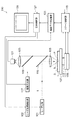
次に、上述したレーザ加工方法に使用されるレーザ加工装置について、図14を参照して説明する。図14はレーザ加工装置100の概略構成図である。
【0038】
レーザ加工装置100は、レーザ光Lを発生するレーザ光源101と、レーザ光Lの出力やパルス幅等を調節するためにレーザ光源101を制御するレーザ光源制御部102と、レーザ光Lの反射機能を有しかつレーザ光Lの光軸の向きを90°変えるように配置されたダイクロイックミラー103と、ダイクロイックミラー103で反射されたレーザ光Lを集光する集光用レンズ105と、集光用レンズ105で集光されたレーザ光Lが照射される加工対象物1が載置される載置台107と、載置台107をX軸方向に移動させるためのX軸ステージ109と、載置台107をX軸方向に直交するY軸方向に移動させるためのY軸ステージ111と、載置台107をX軸及びY軸方向に直交するZ軸方向に移動させるためのZ軸ステージ113と、これら3つのステージ109,111,113の移動を制御するステージ制御部115とを備える。
【0039】
この集光点PのX(Y)軸方向の移動は、加工対象物1をX(Y)軸ステージ109(111)によりX(Y)軸方向に移動させることにより行う。Z軸方向は、加工対象物1の表面3と直交する方向なので、加工対象物1に入射するレーザ光Lの焦点深度の方向となる。よって、Z軸ステージ113をZ軸方向に移動させることにより、加工対象物1の内部にレーザ光Lの集光点Pを合わせることができる。これにより、例えば、加工対象物1が多層構造を有しているような場合に、加工対象物1の基板や或いは当該基板上の積層部等、所望の位置に集光点Pを合わせることができる。
【0040】
レーザ光源101はパルスレーザ光を発生するNd:YAGレーザである。レーザ光源101に用いることができるレーザとして、この他、Nd:YVO4レーザ、Nd:YLFレーザやチタンサファイアレーザがある。本実施形態では、加工対象物1の加工にパルスレーザ光を用いているが、多光子吸収を起こさせることができるなら連続波レーザ光でもよい。
【0041】
レーザ加工装置100はさらに、載置台107に載置された加工対象物1を可視光線により照明するために可視光線を発生する観察用光源117と、ダイクロイックミラー103及び集光用レンズ105と同じ光軸上に配置された可視光用のビームスプリッタ119とを備える。ビームスプリッタ119と集光用レンズ105との間にダイクロイックミラー103が配置されている。ビームスプリッタ119は、可視光線の約半分を反射し残りの半分を透過する機能を有しかつ可視光線の光軸の向きを90°変えるように配置されている。観察用光源117から発生した可視光線はビームスプリッタ119で約半分が反射され、この反射された可視光線がダイクロイックミラー103及び集光用レンズ105を透過し、加工対象物1の切断予定ライン5等を含む表面3を照明する。なお、加工対象物1の裏面が集光用レンズ105側となるよう加工対象物1が載置台107に載置された場合は、ここでいう「表面」が「裏面」となるのは勿論である。
【0042】
レーザ加工装置100はさらに、ビームスプリッタ119、ダイクロイックミラー103及び集光用レンズ105と同じ光軸上に配置された撮像素子121及び結像レンズ123を備える。撮像素子121としては例えばCCDカメラがある。切断予定ライン5等を含む表面3を照明した可視光線の反射光は、集光用レンズ105、ダイクロイックミラー103、ビームスプリッタ119を透過し、結像レンズ123で結像されて撮像素子121で撮像され、撮像データとなる。
【0043】
レーザ加工装置100はさらに、撮像素子121から出力された撮像データが入力される撮像データ処理部125と、レーザ加工装置100全体を制御する全体制御部127と、モニタ129とを備える。撮像データ処理部125は、撮像データを基にして観察用光源117で発生した可視光の焦点を加工対象物1の表面3上に合わせるための焦点データを演算する。この焦点データを基にしてステージ制御部115がZ軸ステージ113を移動制御することにより、可視光の焦点が加工対象物の表面3に合うようにする。よって、撮像データ処理部125はオートフォーカスユニットとして機能する。また、撮像データ処理部125は、撮像データを基にして表面3の拡大画像等の画像データを演算する。この画像データは全体制御部127に送られ、全体制御部で各種処理がなされ、モニタ129に送られる。これにより、モニタ129に拡大画像等が表示される。
【0044】
全体制御部127には、ステージ制御部115からのデータ、撮像データ処理部125からの画像データ等が入力し、これらのデータも基にしてレーザ光源制御部102、観察用光源117及びステージ制御部115を制御することにより、レーザ加工装置100全体を制御する。よって、全体制御部127はコンピュータユニットとして機能する。
【0045】
次に、上述したレーザ加工装置100を使用した場合の切断起点領域形成工程について、図14及び図15を参照して説明する。図15は、本実施形態に係る切断起点領域形成工程を説明するためのフローチャートである。
【0046】
加工対象物1の光吸収特性を図示しない分光光度計等により測定する。この測定結果に基づいて、加工対象物1に対して透明な波長又は吸収の少ない波長のレーザ光Lを発生するレーザ光源101を選定する(S101)。続いて、加工対象物1の厚さを測定する。厚さの測定結果及び加工対象物1の屈折率を基にして、加工対象物1のZ軸方向の移動量を決定する(S103)。これは、レーザ光Lの集光点Pを加工対象物1の基板の内部に位置させるために、加工対象物1の表面3に位置するレーザ光Lの集光点Pを基準とした加工対象物1のZ軸方向の移動量である。この移動量は全体制御部127に入力される。
【0047】
加工対象物1をレーザ加工装置100の載置台107に載置する。そして、観察用光源117から可視光を発生させて加工対象物1を照明する(S105)。照明された切断予定ライン5を含む加工対象物1の表面3を撮像素子121により撮像する。撮像素子121により撮像された撮像データは撮像データ処理部125に送られる。この撮像データに基づいて撮像データ処理部125は観察用光源117の可視光の焦点が表面3に位置するような焦点データを演算する(S107)。
【0048】
この焦点データはステージ制御部115に送られる。ステージ制御部115は、この焦点データを基にしてZ軸ステージ113をZ軸方向の移動させる(S109)。これにより、観察用光源117の可視光の焦点が加工対象物1の表面3に位置する。なお、撮像データ処理部125は撮像データに基づいて、切断予定ライン5を含む加工対象物1の表面3の拡大画像データを演算する。この拡大画像データは全体制御部127を介してモニタ129に送られ、これによりモニタ129に切断予定ライン5付近の拡大画像が表示される。
【0049】
全体制御部127には予めステップS103で決定された移動量データが入力されており、この移動量データがステージ制御部115に送られる。ステージ制御部115はこの移動量データに基づいて、レーザ光Lの集光点Pが加工対象物1の基板の内部となる位置に、Z軸ステージ113により加工対象物1をZ軸方向に移動させる(S111)。
【0050】
続いて、レーザ光源101からレーザ光Lを発生させて、レーザ光Lを加工対象物1の表面3の切断予定ライン5に照射する。レーザ光Lの集光点Pは加工対象物1の基板の内部に位置しているので、改質領域は加工対象物1の基板の内部にのみ形成される。そして、切断予定ライン5に沿うようにX軸ステージ109やY軸ステージ111を移動させて、切断予定ライン5に沿って改質領域を形成し、この改質領域によって、加工対象物1の基板の内部に切断予定ライン5に沿った切断起点領域を形成する(S113)。
以下、実施例により、本発明についてより具体的に説明する。
【0051】
[実施例1]
本発明の実施例1について説明する。なお、図17〜図20は、図16に示す加工対象物1のXVII−XVII線に沿った部分断面図である。
【0052】
図16及び図17に示すように、加工対象物1の裏面21に拡張可能な拡張フィルム(保持部材)19を貼り付けて、この拡張フィルム19の表面19a上に加工対象物1を固定する。拡張フィルム19は、その外周部分がリング状のフィルム固定枠20に貼り付けられて、このフィルム固定枠20に固定されている。なお、この加工対象物1は、厚さ100μmのシリコンウェハである。
【0053】
このように、加工対象物1、拡張フィルム19及びフィルム固定枠20からなるユニットUを、例えば上述のレーザ加工装置100の載置台107上に、加工対象物1の表面3側が集光用レンズ105に対面するように載置する。そして、押え部材107aによりフィルム固定枠20を載置台107に固定すると共に、拡張フィルム19を載置台107に真空吸着する。
【0054】
続いて、図16に示すように、加工対象物1のオリエンテーションフラット16に平行な方向と垂直な方向とに延在する切断予定ライン5を格子状に設定する。この切断予定ラインはウェハ上に形成されている回路素子や受光面などの機能素子からなるデバイス形成面700の間に設定されている。尚、図面では簡略してデバイス形成面700は一部のみに記載している。そして、図17に示すように、加工対象物1の内部に集光点P1を合わせてレーザ光L1を照射し、その集光点P1を切断予定ライン5に沿って移動させることで、加工対象物1の内部に改質領域7を形成する。この改質領域7によって、加工対象物1の表面(レーザ光入射面)3から所定距離内側に切断起点領域8が切断予定ライン5に沿って形成される。なお、加工対象物1がシリコンウェハであるため、改質領域7としては溶融処理領域が形成される。
【0055】
続いて、図18に示すように、加工対象物1の表面3に集光点P2を合わせて、加工対象物1に対して吸収性を有するレーザ光L2を照射し、その集光点P2を切断予定ライン5に沿って移動させる。このレーザ光L2の照射によって、切断起点領域8を起点として割れ24が発生し、この割れ24が加工対象物1の表面3と裏面21とに到達する。これにより、加工対象物1は、切断予定ライン5に沿って複数のチップ25に分割される。
【0056】
このような割れ24の主な発生原因としては、レーザ光L2の照射により切断予定ライン5に沿って加工対象物1が加熱されて、加工対象物1に熱応力が生じることが挙げられる。一例として、レーザ光L2の照射により、改質領域7と加工対象物1の非改質領域(加工対象物1における改質領域7以外の部分)との界面に微細な亀裂や歪みが生じ、これらの亀裂や歪みを起点として加熱源としてのレーザ光L2の照射部位に向かって割れが進展するような引張応力が生じることで、改質領域7から表面3又は裏面21へと割れ24が発生する。
【0057】
なお、実施例1では、レーザ光L2として波長808nm,出力14Wのレーザ光を用い、その光源としてレーザダイオードを用いた。また、集光点P2におけるビーム径は約200μmとした。このようなレーザ光L2の照射によれば、加工対象物1の表面3の溶融を防止しつつ、加工対象物1を加熱することができる。そして、集光点P2におけるビーム径を絞れば絞るほど、加工対象物1を切断予定ライン5に沿って精度良く分割することができる。また、ビーム径を絞ることでウエハ表面に形成されているデバイス形成面間のみにレーザ照射できるので、デバイス形成面に無用なレーザ光L2を照射せずにすみデバイス面を保護できる。
【0058】
加工対象物1を複数のチップ25に切断した後、ユニットUをフィルム拡張装置200に搬送する。図19に示すように、ユニットUは、そのフィルム固定枠20がリング状の受け部材201とリング状の押え部材202とで挟持されて、フィルム拡張装置200に固定される。そして、受け部材201の内側に配置された円柱状の押圧部材203をユニットUの下側から拡張フィルム19の裏面19bに押し当て、さらに、図20に示すように押圧部材203を上昇させる。これにより、拡張フィルム19における各チップ25の接触部分が外方側に拡張されて各チップ25が互いに離間することになり、各チップ25を容易且つ確実にピックアップすることが可能になる。
【0059】
以上の実施例1に係るレーザ加工方法においては、多光子吸収により形成される改質領域7によって、切断予定ライン5に沿って加工対象物1の内部に切断起点領域8を形成することができる。そして、加工対象物1に対して吸収性を有するレーザ光L2を切断予定ライン5に沿って加工対象物1に照射することで、切断起点領域5を起点として加工対象物1に割れ24を発生させ、切断予定ライン5に沿って加工対象物1を精度良く切断することができる。しかも、加工対象物1が固定された拡張フィルム19を拡張させることで、各チップ25が離間することになるため、切断予定ライン5に沿った加工対象物1の切断の確実性をより一層向上させることができる。
【0060】
[実施例2]
本発明の実施例2について説明する。実施例2は、レーザ光L2を照射した際に発生する割れ24が加工対象物1の表面3と裏面21とに到達しない点で、実施例1と異なる。以下、この実施例1との相異点を中心に説明する。なお、図21は、図16に示す加工対象物1のXVII−XVII線に沿った部分断面図である。
【0061】
実施例1と同様に、加工対象物1、拡張フィルム19及びフィルム固定枠20からなるユニットUを用意し、例えば上述のレーザ加工装置100を用いて加工対象物1の内部に改質領域7を形成し、この改質領域7によって、加工対象物1の表面3から所定距離内側に切断起点領域8を切断予定ライン5に沿って形成する。なお、加工対象物1は、厚さ300μmのシリコンウェハである。
【0062】
続いて、図21に示すように、加工対象物1の表面3に集光点P2を合わせて、加工対象物1に対して吸収性を有するレーザ光L2を照射し、その集光点P2を切断予定ライン5に沿って移動させる。このレーザ光L2の照射によって、切断起点領域8を起点として割れ24が発生する。ただし、実施例2の加工対象物1の厚さ(300μm)は実施例1の加工対象物1の厚さ(100μm)に比べて厚いため、割れ24は、加工対象物1の表面3と裏面21とには到達せず、加工対象物1の内部に留まる。なお、レーザ光L2の照射条件は実施例1と同様である。
【0063】
続いて、実施例1と同様に、ユニットUをフィルム拡張装置200に搬送する。そして、フィルム拡張装置200において、ユニットUの下側から拡張フィルム19の裏面19bに押圧部材203押し当て、さらに、この押圧部材203を上昇させる。これにより、拡張フィルム19における加工対象物1の接触部分が外方側に拡張される。この拡張フィルム19の拡張に伴い、加工対象物1内の割れ24の先端が加工対象物1の表面3と裏面21とに到達して、加工対象物1が切断予定ライン5に沿って複数の各チップ25に分割され、各チップ25が互いに離間することになる。
【0064】
なお、レーザ光L2の照射条件によっては、レーザ光L2の照射時に割れ24が発生しない場合がある。このような場合であっても、レーザ光L2を照射しない場合に比べれば、拡張フィルム19の拡張によって、加工対象物1を切断予定ライン5に沿って容易且つ高精度に分割することができる。
【0065】
以上の実施例2に係るレーザ加工方法においては、上述した実施例1に係るレーザ加工方法と同様に、切断予定ライン5に沿って加工対象物1の内部に切断起点領域8を形成することができる。そして、加工対象物1に対して吸収性を有するレーザ光L2を切断予定ライン5に沿って加工対象物1に照射することで、このような照射を行わない場合に比べて小さな力によって、切断起点領域8を起点とした割れ24を加工対象物1の表面3と裏面21とに到達させることができる。したがって、加工対象物1が固定された拡張フィルム19をより小さな力で拡張させることができ、切断予定ライン5に沿って加工対象物1を精度良く切断することが可能になる。しかも、この拡張フィルム19を拡張させることで、各チップ24が離間することになるため、切断予定ライン5に沿った加工対象物1の切断の確実性をより一層向上させることができる。
【0066】
本発明は、上述した実施例1及び実施例2には限定されない。
【0067】
例えば、加工対象物1の材料、及びその加工対象物1に対して吸収性を有するレーザ光L2の種類としては、次のようなものが好ましい。すなわち、加工対象物1がシリコンウェハやGaAs系ウェハの場合は、レーザ光L2として、波長が500nm〜1100nmのレーザ光を用いることが好ましい。具体的には、YAGレーザの2倍波(波長532nm)、GaAs系の半導体レーザ(波長780nmや波長808nm)、Ndドープのファイバーレーザ(波長1060nm)等がある。また、加工対象物1がガラスの場合は、レーザ光L2として、波長が2μm以上のレーザ光を用いることが好ましい。具体的には、CO2レーザ(波長10.6μm)、COレーザ(波長約5.5μm)、フッ化水素レーザ(波長約2.9μm)等がある。
【0068】
また、レーザ光L2の照射により発生する割れ24を加工対象物1の表面3又は裏面21のいずれか一方に到達させてもよい。このような制御は、加工対象物1の厚さ方向における中心位置から表面3又は裏面21のいずれか一方に偏倚させて改質領域7を形成することで可能になる。特に、レーザ光L2の照射により割れ24を加工対象物1の拡張フィルム19側の面に到達させると、拡張フィルム19の拡張による加工対象物1の割断精度をより一層向上させることができる。
【0069】
なお、「加工対象物1の厚さ方向における中心位置から加工対象物1の表面3側に偏倚させて改質領域7を形成する」とは、切断起点領域8を構成する改質領域7が、加工対象物1の厚さ方向における厚さの半分の位置から表面3側に偏倚して形成されることを意味する。つまり、加工対象物1の厚さ方向における改質領域7の幅の中心位置が、加工対象物1の厚さ方向における中心位置から表面3側に偏倚して位置している場合を意味し、改質領域7の全ての部分が加工対象物1の厚さ方向における中心位置に対して表面3側に位置している場合のみに限る意味ではない。加工対象物1の裏面21側に偏倚させて改質領域7を形成する場合についても同様である。
【0070】
また、上述したレーザ光L2の照射は切断予定ライン5上への照射であったが、切断予定ライン5近傍への照射であってもよい。また、レーザ光L2の集光点P2の位置は加工対象物1の表面3上でなくてもよい。
【0071】
【発明の効果】
本発明に係るレーザ加工方法によれば、切断予定ラインに沿って加工対象物を確実且つ高精度に切断することができる。
【図面の簡単な説明】
【図1】本実施形態に係るレーザ加工方法によるレーザ加工中の加工対象物の平面図である。
【図2】図1に示す加工対象物のII−II線に沿った断面図である。
【図3】本実施形態に係るレーザ加工方法によるレーザ加工後の加工対象物の平面図である。
【図4】図3に示す加工対象物のIV−IV線に沿った断面図である。
【図5】図3に示す加工対象物のV−V線に沿った断面図である。
【図6】本実施形態に係るレーザ加工方法により切断された加工対象物の平面図である。
【図7】本実施形態に係るレーザ加工方法における電界強度とクラックスポットの大きさとの関係を示すグラフである。
【図8】本実施形態に係るレーザ加工方法の第1工程における加工対象物の断面図である。
【図9】本実施形態に係るレーザ加工方法の第2工程における加工対象物の断面図である。
【図10】本実施形態に係るレーザ加工方法の第3工程における加工対象物の断面図である。
【図11】本実施形態に係るレーザ加工方法の第4工程における加工対象物の断面図である。
【図12】本実施形態に係るレーザ加工方法により切断されたシリコンウェハの一部における断面の写真を表した図である。
【図13】本実施形態に係るレーザ加工方法におけるレーザ光の波長とシリコン基板の内部の透過率との関係を示すグラフである。
【図14】本実施形態に係るレーザ加工装置の概略構成図である。
【図15】本実施形態に係る切断起点領域形成工程を説明するためのフローチャートである。
【図16】実施例1に係る加工対象物の平面図である。
【図17】実施例1に係る加工対象物に切断起点領域を形成している様子を示す断面図である。
【図18】実施例1に係る加工対象物に吸収性を有するレーザ光を照射している様子を示す断面図である。
【図19】実施例1に係る加工対象物をフィルム拡張装置にセットした様子を示す断面図である。
【図20】実施例1に係る加工対象物が固定された拡張フィルムを拡張させた様子を示す断面図である。
【図21】実施例2に係る加工対象物に吸収性を有するレーザ光を照射している様子を示す断面図である。
【符号の説明】
1…加工対象物、3…加工対象物の表面(レーザ光入射面)、5…切断予定ライン、7…改質領域、8…切断起点領域、19…拡張フィルム(保持部材)、19a…拡張フィルムの表面、25…チップ、L,L1,L2…レーザ光、P,P1,P2…集光点。[0001]
BACKGROUND OF THE INVENTION
[0002]
The present invention relates to a laser processing method used for cutting an object to be processed such as a semiconductor material substrate, a piezoelectric material substrate or a glass substrate.
[0003]
[Prior art]
The following
[0004]
[Patent Document 1]
International Publication No. 02/22301 Pamphlet [0005]
[Problems to be solved by the invention]
Since the technique described in
[0006]
Then, this invention is made | formed in view of such a situation, and it aims at providing the laser processing method which can cut | disconnect a process target object reliably and with high precision along a cutting plan line. .
[0007]
[Means for Solving the Problems]
In order to achieve the above object, a laser processing method according to the present invention irradiates a laser beam with a condensing point inside a wafer-like processing object fixed to the surface of an expandable holding member, and performs processing. Forming a modified region in the interior of the object, and forming a cutting start region in a predetermined distance from the laser light incident surface of the processing object along the planned cutting line of the processing object by the modified region; After the step of forming the cutting start region, a step of cutting the processing object along the planned cutting line by irradiating the processing target along the planned cutting line with laser light having absorbency with respect to the processing target And after the step of cutting the workpiece, the holding member is expanded to separate the portions of the cut workpiece.
[0008]
In this laser processing method, the cutting start region can be formed inside the processing object along a desired cutting line to be processed by the modified region formed by multiphoton absorption. Then, by irradiating the processing object along the planned cutting line with a laser beam having absorbency with respect to the processing target, the processing target is cracked starting from the cutting start region, and along the planned cutting line. The workpiece can be cut with high accuracy. In addition, by extending the holding member to which the workpiece is fixed, each part of the workpiece is separated, so the reliability of cutting the workpiece along the planned cutting line is further improved. Can be made.
[0009]
Further, the laser processing method according to the present invention irradiates a laser beam with a focusing point inside the wafer-like workpiece fixed on the surface of the expandable holding member, and modifies the inside of the workpiece. And forming a cutting start area by a predetermined distance inside the laser light incident surface of the processing object along the planned cutting line of the processing object, and a cutting starting area. After the process, after the process of irradiating the processing object with a laser beam having absorptivity to the processing object and the process of irradiating the processing object, the holding member is expanded to expand the processing object. Cutting the object, and separating each part of the cut object to be processed.
[0010]
In this laser processing method, similarly to the laser processing method described above, it is possible to form the cutting start region along the planned cutting line inside the workpiece. Then, by irradiating the processing object with a laser beam having absorptivity to the processing object along the planned cutting line, the starting point of the cutting start area can be set with a small force compared to the case where such irradiation is not performed. It is possible to reach the front and back surfaces of the workpiece. Therefore, the holding member to which the workpiece is fixed can be expanded with a smaller force, and the workpiece can be accurately cut along the scheduled cutting line. In addition, by expanding the holding member, the respective parts of the workpiece are separated from each other, so that the certainty of cutting the workpiece along the planned cutting line can be further improved.
[0011]
In addition, a condensing point is a location which the laser beam condensed. In addition, the cutting start region means a region that becomes a starting point of cutting when the workpiece is cut. Therefore, the cutting start region is a planned cutting portion where cutting is planned for the workpiece. The cutting start region may be formed by continuously forming the modified region, or may be formed by intermittently forming the modified region. In addition, the object to be processed may be formed of a semiconductor material, and the modified region may be a melt processing region.
[0012]
DETAILED DESCRIPTION OF THE INVENTION
DESCRIPTION OF EMBODIMENTS Hereinafter, preferred embodiments of the present invention will be described in detail with reference to the drawings. In the step of forming the cutting start region in the laser processing method according to the present embodiment (hereinafter referred to as “cutting start region forming step”), the processing target is irradiated with a laser beam with the focusing point inside the processing target. A modified region by multiphoton absorption is formed inside the object. This laser processing method, particularly multiphoton absorption, will be described first.
[0013]
Photon energy hν is smaller than the band gap E G of absorption of the material becomes transparent. Therefore, a condition under which absorption occurs in the material is hv> E G. However, even when optically transparent, increasing the intensity of the laser beam very Nhnyu> of E G condition (n = 2,3,4, ···) the intensity of laser light becomes very high. This phenomenon is called multiphoton absorption. In the case of a pulse wave, the intensity of the laser beam is determined by the peak power density (W / cm 2 ) at the condensing point of the laser beam. For example, the multiphoton is obtained under conditions where the peak power density is 1 × 10 8 (W / cm 2 ) or more. Absorption occurs. The peak power density is determined by (energy per pulse of laser light at the condensing point) / (laser beam cross-sectional area of laser light × pulse width). In the case of a continuous wave, the intensity of the laser beam is determined by the electric field intensity (W / cm 2 ) at the condensing point of the laser beam.
[0014]
The principle of laser processing according to this embodiment using such multiphoton absorption will be described with reference to FIGS. FIG. 1 is a plan view of a
[0015]
As shown in FIGS. 1 and 2, the
[0016]
The condensing point P is moved along the
[0017]
In the cutting of the
[0018]
It should be noted that the following two methods are conceivable for cutting the object to be processed starting from the cutting start region. One is a case where an artificial force is applied to the workpiece after the cutting start region is formed, so that the workpiece is broken starting from the cutting start region and the workpiece is cut. This is, for example, cutting when the thickness of the workpiece is large. An artificial force is applied when, for example, bending stress or shear stress is applied to the workpiece along the cutting start region of the workpiece, or thermal stress is generated by giving a temperature difference to the workpiece. It is to let you. The other is that when the cutting start region is formed, the cutting start region is used as a starting point, and the workpiece is naturally cracked in the cross-sectional direction (thickness direction) of the processing target, resulting in the processing target being cut. It is. For example, when the thickness of the workpiece is small, the cutting start region is formed by one row of modified regions, and when the thickness of the workpiece is large, the thickness direction This is made possible by forming the cutting start region by the modified regions formed in a plurality of rows. In addition, even when this breaks naturally, in the part to be cut, the part corresponding to the part where the cutting starting point region is formed without cracking ahead on the surface of the part corresponding to the part where the cutting starting point region is not formed Since it is possible to cleave only, the cleaving can be controlled well. In recent years, since the thickness of workpieces such as silicon wafers tends to be thin, such a cleaving method with good controllability is very effective.
[0019]
In the present embodiment, the modified regions formed by multiphoton absorption include the following (1) to (3).
[0020]
(1) In the case where the modified region is a crack region including one or more cracks, the focusing point is set inside the object to be processed (for example, piezoelectric material made of glass or LiTaO 3 ), and the electric field strength at the focusing point is Irradiation with laser light is performed under conditions of 1 × 10 8 (W / cm 2 ) or more and a pulse width of 1 μs or less. The magnitude of this pulse width is a condition that allows a crack region to be formed only inside the workpiece without causing extra damage to the surface of the workpiece while causing multiphoton absorption. As a result, a phenomenon of optical damage due to multiphoton absorption occurs inside the workpiece. This optical damage induces thermal strain inside the workpiece, thereby forming a crack region inside the workpiece. The upper limit value of the electric field strength is, for example, 1 × 10 12 (W / cm 2 ). The pulse width is preferably 1 ns to 200 ns, for example. The formation of the crack region by multiphoton absorption is described in, for example, “Inside of glass substrate by solid-state laser harmonics” on pages 23-28 of the 45th Laser Thermal Processing Research Papers (December 1998). It is described in “Marking”.
[0021]
The inventor obtained the relationship between the electric field strength and the size of the cracks by experiment. The experimental conditions are as follows.
[0022]
(A) Workpiece: Pyrex (registered trademark) glass (
(B) Laser light source: semiconductor laser excitation Nd: YAG laser wavelength: 1064 nm
Laser light spot cross-sectional area: 3.14 × 10 −8 cm 2
Oscillation form: Q switch pulse repetition frequency: 100 kHz
Pulse width: 30ns
Output: Output <1 mJ / pulse laser light quality: TEM 00
Polarization characteristics: Linearly polarized light (C) Condensation lens Transmittance with respect to laser beam wavelength: 60% (D) Moving speed of mounting table on which workpiece is mounted: 100 mm / second
Note that the laser light quality TEM 00 means that the light condensing performance is high and the light can be condensed up to the wavelength of the laser light.
[0024]
FIG. 7 is a graph showing the results of the experiment. The horizontal axis represents the peak power density. Since the laser beam is a pulsed laser beam, the electric field strength is represented by the peak power density. The vertical axis represents the size of a crack portion (crack spot) formed inside the workpiece by one pulse of laser light. Crack spots gather to form a crack region. The size of the crack spot is the size of the portion having the maximum length in the shape of the crack spot. Data indicated by black circles in the graph is for the case where the magnification of the condenser lens (C) is 100 times and the numerical aperture (NA) is 0.80. On the other hand, the data indicated by the white circles in the graph is when the magnification of the condenser lens (C) is 50 times and the numerical aperture (NA) is 0.55. From the peak power density of about 10 11 (W / cm 2 ), it can be seen that a crack spot is generated inside the workpiece, and the crack spot increases as the peak power density increases.
[0025]
Next, in the laser processing according to the present embodiment, a mechanism for cutting a workpiece by forming a crack region will be described with reference to FIGS. As shown in FIG. 8, the laser beam L is irradiated to the
[0026]
(2) When the modified region is a melted region, the focusing point is set inside the object to be processed (for example, a semiconductor material such as silicon), and the electric field strength at the focusing point is 1 × 10 8 (W / cm 2). ) Irradiation with laser light is performed under the above conditions with a pulse width of 1 μs or less. As a result, the inside of the workpiece is locally heated by multiphoton absorption. By this heating, a melt processing region is formed inside the workpiece. The melt treatment region is a region once solidified after melting, a region in a molten state, or a region re-solidified from a molten state, and can also be referred to as a phase-changed region or a region in which the crystal structure has changed. The melt treatment region can also be said to be a region in which one structure is changed to another structure in a single crystal structure, an amorphous structure, or a polycrystalline structure. In other words, for example, a region changed from a single crystal structure to an amorphous structure, a region changed from a single crystal structure to a polycrystalline structure, or a region changed from a single crystal structure to a structure including an amorphous structure and a polycrystalline structure. To do. When the object to be processed has a silicon single crystal structure, the melt processing region has, for example, an amorphous silicon structure. The upper limit value of the electric field strength is, for example, 1 × 10 12 (W / cm 2 ). The pulse width is preferably 1 ns to 200 ns, for example.
[0027]
The inventor has confirmed through experiments that a melt-processed region is formed inside a silicon wafer. The experimental conditions are as follows.
[0028]
(A) Workpiece: silicon wafer (thickness 350 μm, outer diameter 4 inches)
(B) Laser light source: semiconductor laser excitation Nd: YAG laser wavelength: 1064 nm
Laser light spot cross-sectional area: 3.14 × 10 −8 cm 2
Oscillation form: Q switch pulse repetition frequency: 100 kHz
Pulse width: 30ns
Output: 20 μJ / pulse laser light Quality: TEM 00
Polarization characteristics: Linearly polarized light (C) Condensing lens magnification: 50 × N. A. : 0.55
Transmittance with respect to wavelength of laser beam: 60% (D) Moving speed of mounting table on which workpiece is mounted: 100 mm / second
FIG. 12 is a view showing a photograph of a cross section of a part of a silicon wafer cut by laser processing under the above conditions. A
[0030]
The fact that the
[0031]
For example, when the thickness of the silicon substrate is 500 μm or less at the wavelength of the Nd: YAG laser of 1064 nm, it can be seen that the laser light is transmitted by 80% or more inside the silicon substrate. Since the thickness of the
[0032]
Silicon wafers are cracked in the cross-sectional direction starting from the cutting start region formed by the melt processing region, and the cracks reach the front and back surfaces of the silicon wafer, resulting in cutting. Is done. The cracks that reach the front and back surfaces of the silicon wafer may grow naturally or may grow by applying force to the silicon wafer. In addition, when a crack naturally grows from the cutting start region to the front and back surfaces of the silicon wafer, the case where the crack grows from a state where the melt treatment region forming the cutting starting region is melted, and the cutting starting region There are both cases where cracks grow when the solidified region is melted from the molten state. However, in either case, the melt processing region is formed only inside the silicon wafer, and the melt processing region is formed only inside the cut surface after cutting as shown in FIG. When the cutting start region is formed in the object to be processed by the melt processing region, unnecessary cracking off the cutting start region line is less likely to occur at the time of cleaving, so that cleaving control is facilitated.
[0033]
(3) In the case where the modified region is a refractive index changing region, the focusing point is set inside the object to be processed (for example, glass), and the electric field intensity at the focusing point is 1 × 10 8 (W / cm 2 ) or more. Laser light is irradiated under the condition that the pulse width is 1 ns or less. When the pulse width is made extremely short and multiphoton absorption occurs inside the workpiece, the energy due to the multiphoton absorption is not converted into thermal energy, and the ion valence change and crystallization occur inside the workpiece. Alternatively, a permanent structural change such as polarization orientation is induced to form a refractive index change region. The upper limit value of the electric field strength is, for example, 1 × 10 12 (W / cm 2 ). For example, the pulse width is preferably 1 ns or less, and more preferably 1 ps or less. The formation of the refractive index change region by multiphoton absorption is described in, for example, “The Femtosecond Laser Irradiation to the Inside of the Glass” on
[0034]
As described above, the cases of (1) to (3) have been described as the modified regions formed by multiphoton absorption. However, considering the crystal structure of the wafer-like workpiece and its cleavage property, the cutting origin region is described below. If it forms in this way, it will become possible to cut | disconnect a process target object with much smaller force from the cutting | disconnection starting point area | region as a starting point, and still more accurately.
[0035]
That is, in the case of a substrate made of a single crystal semiconductor having a diamond structure such as silicon, the cutting start region is formed in a direction along the (111) plane (first cleavage plane) or the (110) plane (second cleavage plane). Is preferred. In the case of a substrate made of a zinc-blende-type III-V group compound semiconductor such as GaAs, it is preferable to form the cutting start region in the direction along the (110) plane. Further, in the case of a substrate having a hexagonal crystal structure such as sapphire (Al 2 O 3 ), the (1120) plane (A plane) or (1100) plane ( It is preferable to form the cutting start region in a direction along the (M plane).
[0036]
Note that the orientation flat on the substrate along the direction in which the above-described cutting start region is to be formed (for example, the direction along the (111) plane in the single crystal silicon substrate) or the direction perpendicular to the direction in which the cutting start region is to be formed. By using the orientation flat as a reference, it is possible to easily and accurately form the cutting start area along the direction in which the cutting start area is to be formed on the substrate.
[0037]
Next, a laser processing apparatus used in the laser processing method described above will be described with reference to FIG. FIG. 14 is a schematic configuration diagram of the
[0038]
The
[0039]
The converging point P is moved in the X (Y) axis direction by moving the
[0040]
The
[0041]
The
[0042]
The
[0043]
The
[0044]
Data from the
[0045]
Next, the cutting start region forming step when using the above-described
[0046]
The light absorption characteristics of the
[0047]
The
[0048]
This focus data is sent to the
[0049]
The movement amount data determined in advance in step S <b> 103 is input to the
[0050]
Subsequently, the laser light L is generated from the
Hereinafter, the present invention will be described more specifically with reference to examples.
[0051]
[Example 1]
Example 1 of the present invention will be described. 17 to 20 are partial cross-sectional views along the line XVII-XVII of the
[0052]
As shown in FIGS. 16 and 17, an expandable expansion film (holding member) 19 is attached to the
[0053]
As described above, the unit U including the
[0054]
Subsequently, as shown in FIG. 16, the
[0055]
Subsequently, as shown in FIG. 18, the focused point P2 is aligned with the
[0056]
The main cause of the occurrence of such a
[0057]
In Example 1, a laser beam having a wavelength of 808 nm and an output of 14 W was used as the laser beam L2, and a laser diode was used as the light source. The beam diameter at the condensing point P2 was about 200 μm. According to such irradiation of the laser beam L2, the
[0058]
After the
[0059]
In the laser processing method according to the first embodiment, the cutting
[0060]
[Example 2]
A second embodiment of the present invention will be described. The second embodiment is different from the first embodiment in that the
[0061]
As in the first embodiment, a unit U including the
[0062]
Subsequently, as shown in FIG. 21, the focused point P2 is aligned with the
[0063]
Subsequently, the unit U is transported to the
[0064]
Note that, depending on the irradiation condition of the laser beam L2, the
[0065]
In the laser processing method according to the second embodiment, the cutting
[0066]
The present invention is not limited to the first and second embodiments described above.
[0067]
For example, the following are preferable as the material of the
[0068]
Moreover, you may make the
[0069]
Note that “the modified
[0070]
Moreover, although the irradiation of the laser beam L2 described above is irradiation on the
[0071]
【The invention's effect】
According to the laser processing method according to the present invention, it is possible to reliably and highly accurately cut the object to be processed along the scheduled cutting line.
[Brief description of the drawings]
FIG. 1 is a plan view of an object to be processed during laser processing by a laser processing method according to an embodiment.
2 is a cross-sectional view taken along line II-II of the workpiece shown in FIG.
FIG. 3 is a plan view of an object to be processed after laser processing by the laser processing method according to the present embodiment.
4 is a cross-sectional view taken along line IV-IV of the workpiece shown in FIG.
5 is a cross-sectional view taken along line VV of the workpiece shown in FIG.
FIG. 6 is a plan view of a processing object cut by the laser processing method according to the present embodiment.
FIG. 7 is a graph showing the relationship between electric field strength and crack spot size in the laser processing method according to the present embodiment.
FIG. 8 is a cross-sectional view of an object to be processed in a first step of the laser processing method according to the present embodiment.
FIG. 9 is a cross-sectional view of an object to be processed in a second step of the laser processing method according to the present embodiment.
FIG. 10 is a cross-sectional view of an object to be processed in a third step of the laser processing method according to the present embodiment.
FIG. 11 is a cross-sectional view of an object to be processed in a fourth step of the laser processing method according to the present embodiment.
FIG. 12 is a view showing a photograph of a cross section of a part of a silicon wafer cut by the laser processing method according to the embodiment.
FIG. 13 is a graph showing the relationship between the wavelength of laser light and the transmittance inside the silicon substrate in the laser processing method according to the present embodiment.
FIG. 14 is a schematic configuration diagram of a laser processing apparatus according to the present embodiment.
FIG. 15 is a flowchart for explaining a cutting start region forming process according to the embodiment;
FIG. 16 is a plan view of a workpiece according to the first embodiment.
FIG. 17 is a cross-sectional view illustrating a state in which a cutting start region is formed on the workpiece according to the first embodiment.
18 is a cross-sectional view showing a state in which a processing target according to Example 1 is irradiated with absorptive laser light. FIG.
FIG. 19 is a cross-sectional view showing a state in which the object to be processed according to Example 1 is set in a film expansion device.
FIG. 20 is a cross-sectional view showing a state in which an expansion film to which a workpiece according to Example 1 is fixed is expanded.
FIG. 21 is a cross-sectional view showing a state in which a processing target according to Example 2 is irradiated with absorptive laser light.
[Explanation of symbols]
DESCRIPTION OF
Claims (3)
前記切断起点領域を形成する工程後、前記加工対象物に対して吸収性を有するレーザ光を前記切断予定ラインに沿って前記加工対象物に照射することで、前記切断予定ラインに沿って前記加工対象物を切断する工程と、
前記加工対象物を切断する工程後、前記保持部材を拡張させることで、切断された前記加工対象物のそれぞれの部分を離間させる工程とを備えることを特徴とするレーザ加工方法。A modified region is formed inside the workpiece by irradiating a laser beam with a focusing point inside the wafer-like workpiece fixed on the surface of the expandable holding member. A step of forming a cutting start region on a predetermined distance inside from a laser light incident surface of the processing object along a cutting planned line of the processing object;
After the step of forming the cutting start region, the processing target is irradiated along the planned cutting line by irradiating the processing target along the planned cutting line with a laser beam having an absorptivity with respect to the processing target. Cutting the object;
And a step of separating the respective portions of the cut object to be processed by expanding the holding member after the step of cutting the object to be processed.
前記切断起点領域を形成する工程後、前記加工対象物に対して吸収性を有するレーザ光を前記切断予定ラインに沿って前記加工対象物に照射する工程と、
前記加工対象物に照射する工程後、前記保持部材を拡張させることで、前記加工対象物を切断し、かつ切断された前記加工対象物のそれぞれの部分を離間させる工程とを備えることを特徴とするレーザ加工方法。A modified region is formed inside the workpiece by irradiating a laser beam with a focusing point inside the wafer-like workpiece fixed on the surface of the expandable holding member. A step of forming a cutting start region on a predetermined distance inside from a laser light incident surface of the processing object along a cutting planned line of the processing object;
After the step of forming the cutting start region, irradiating the processing object along the planned cutting line with laser light having absorbency with respect to the processing object;
After the step of irradiating the workpiece, the holding member is expanded to cut the workpiece and to separate the cut portions of the workpiece. Laser processing method.
Priority Applications (1)
| Application Number | Priority Date | Filing Date | Title |
|---|---|---|---|
| JP2003063777A JP2004268103A (en) | 2003-03-10 | 2003-03-10 | Laser beam machining method |
Applications Claiming Priority (1)
| Application Number | Priority Date | Filing Date | Title |
|---|---|---|---|
| JP2003063777A JP2004268103A (en) | 2003-03-10 | 2003-03-10 | Laser beam machining method |
Publications (2)
| Publication Number | Publication Date |
|---|---|
| JP2004268103A true JP2004268103A (en) | 2004-09-30 |
| JP2004268103A5 JP2004268103A5 (en) | 2006-04-27 |
Family
ID=33125270
Family Applications (1)
| Application Number | Title | Priority Date | Filing Date |
|---|---|---|---|
| JP2003063777A Pending JP2004268103A (en) | 2003-03-10 | 2003-03-10 | Laser beam machining method |
Country Status (1)
| Country | Link |
|---|---|
| JP (1) | JP2004268103A (en) |
Cited By (4)
| Publication number | Priority date | Publication date | Assignee | Title |
|---|---|---|---|---|
| JP2007118207A (en) * | 2005-10-25 | 2007-05-17 | Seiko Epson Corp | Processing method of laminate |
| JP2013126683A (en) * | 2011-11-18 | 2013-06-27 | Hamamatsu Photonics Kk | Laser beam machining method |
| JP2014176901A (en) * | 2009-04-07 | 2014-09-25 | Hamamatsu Photonics Kk | Laser processing apparatus and laser processing method |
| JP2020061398A (en) * | 2018-10-05 | 2020-04-16 | 株式会社ディスコ | Processing method for wafer |
-
2003
- 2003-03-10 JP JP2003063777A patent/JP2004268103A/en active Pending
Cited By (6)
| Publication number | Priority date | Publication date | Assignee | Title |
|---|---|---|---|---|
| JP2007118207A (en) * | 2005-10-25 | 2007-05-17 | Seiko Epson Corp | Processing method of laminate |
| JP2014176901A (en) * | 2009-04-07 | 2014-09-25 | Hamamatsu Photonics Kk | Laser processing apparatus and laser processing method |
| US9035216B2 (en) | 2009-04-07 | 2015-05-19 | Hamamatsu Photonics K.K. | Method and device for controlling interior fractures by controlling the laser pulse width |
| KR101769158B1 (en) * | 2009-04-07 | 2017-08-17 | 하마마츠 포토닉스 가부시키가이샤 | Laser machining device and laser machining method |
| JP2013126683A (en) * | 2011-11-18 | 2013-06-27 | Hamamatsu Photonics Kk | Laser beam machining method |
| JP2020061398A (en) * | 2018-10-05 | 2020-04-16 | 株式会社ディスコ | Processing method for wafer |
Similar Documents
| Publication | Publication Date | Title |
|---|---|---|
| JP4606741B2 (en) | Processing object cutting method | |
| JP4322881B2 (en) | Laser processing method and laser processing apparatus | |
| JP3626442B2 (en) | Laser processing method | |
| JP3722731B2 (en) | Laser processing method | |
| JP4837320B2 (en) | Processing object cutting method | |
| JP3670267B2 (en) | Laser processing method | |
| WO2004080643A1 (en) | Laser beam machining method | |
| JP3761567B2 (en) | Laser processing method | |
| JP4664140B2 (en) | Laser processing method | |
| JP4167094B2 (en) | Laser processing method | |
| JP4659301B2 (en) | Laser processing method | |
| JP4409840B2 (en) | Processing object cutting method | |
| JP2005159378A (en) | Laser beam machining method | |
| JP2003088973A (en) | Laser beam machining method | |
| JP4509720B2 (en) | Laser processing method | |
| JP3751970B2 (en) | Laser processing equipment | |
| JP3867109B2 (en) | Laser processing method | |
| JP3990710B2 (en) | Laser processing method | |
| JP3867110B2 (en) | Laser processing method | |
| JP3867108B2 (en) | Laser processing equipment | |
| JP2003088974A (en) | Laser beam machining method | |
| WO2004080642A1 (en) | Laser beam machining method | |
| JP3761566B2 (en) | Manufacturing method of semiconductor chip | |
| JP4146863B2 (en) | Semiconductor substrate cutting method | |
| JP3867003B2 (en) | Laser processing method |
Legal Events
| Date | Code | Title | Description |
|---|---|---|---|
| A521 | Written amendment |
Free format text: JAPANESE INTERMEDIATE CODE: A523 Effective date: 20060309 |
|
| A621 | Written request for application examination |
Free format text: JAPANESE INTERMEDIATE CODE: A621 Effective date: 20060309 |
|
| A977 | Report on retrieval |
Free format text: JAPANESE INTERMEDIATE CODE: A971007 Effective date: 20080718 |
|
| A131 | Notification of reasons for refusal |
Free format text: JAPANESE INTERMEDIATE CODE: A131 Effective date: 20080729 |
|
| A02 | Decision of refusal |
Free format text: JAPANESE INTERMEDIATE CODE: A02 Effective date: 20081202 |