JP2004265964A - Alignment method, alignment equipment, aligner, and method for manufacturing semiconductor device - Google Patents
Alignment method, alignment equipment, aligner, and method for manufacturing semiconductor device Download PDFInfo
- Publication number
- JP2004265964A JP2004265964A JP2003052416A JP2003052416A JP2004265964A JP 2004265964 A JP2004265964 A JP 2004265964A JP 2003052416 A JP2003052416 A JP 2003052416A JP 2003052416 A JP2003052416 A JP 2003052416A JP 2004265964 A JP2004265964 A JP 2004265964A
- Authority
- JP
- Japan
- Prior art keywords
- light
- mask
- wafer
- alignment mark
- alignment
- Prior art date
- Legal status (The legal status is an assumption and is not a legal conclusion. Google has not performed a legal analysis and makes no representation as to the accuracy of the status listed.)
- Pending
Links
Images


Abstract
Description
【0001】
【発明の属する技術分野】
本発明は、半導体装置製造のリソグラフィ工程などで用いられるマスクなどのアライメント方法およびアライメント装置と、それを用いた露光装置と半導体装置の製造方法に関する。
【0002】
【従来の技術】
フォトリソグラフィに代わる次世代露光技術として、電子線やX線を用いて、マスクを被露光ウエハに近接させて露光する、電子線近接リソグラフィや等倍X線リソグラフィなどの転写型露光方法が開発されている。
これらのリソグラフィにおいて用いられるマスクは、例えば0.5μmの膜厚のSi膜やSiC膜、ダイヤモンドなどの薄膜から構成される。
【0003】
上記の次世代露光技術においては、例えばマスクと被露光ウエハの相対位置をリアルタイムに測定して位置合わせするアライメント装置が使用される。
例えば、被露光ウエハに形成されたレジスト膜を感光させないような長波長光を用いており、マスクとウエハに書き込まれたアライメントマークに測定用の光(照明光)を照射し、各アライメントマークで散乱されて戻ってくる光を検出して撮像素子に結像し、画像処理を行ってアライメントマークの位置を測定し、マスクとウエハの位置ずれを検出する。
上記のようにして得られたマスクとウエハの位置ずれを補正するように、ウエハに対するマスクの位置を調節して位置合わせする。
【0004】
例えば、特許文献1に記載の露光方法においては、投影光学系のベストフォーカス位置を求める方法が記載されている。
この方法では、レジスト膜が形成されたウエハ上の周辺の未露光領域に、投影光学系に対するフォーカス位置を変えて焦点計測用マークの潜像パターンを露光し、潜像パターンに対して斜めの方向から2つの検出ビームを照射し、潜像パターンから平行に発生する1組の回折光の干渉光の強度を求め、干渉光の強度が最大となるフォーカス位置をベストフォーカス位置とする。
【0005】
上記のようなアライメント方法の1つであるホログラムやフレネルゾーンプレートを利用したアライメント方法は、単なるアライメントパターンを用いた方法に比較してアライメントパターンの形状歪に影響されずに高精度にアライメントできる特徴がある。
ホログラムやフレネルゾーンプレートを用いてマスクとウエハの相対的位置合せを行う場合、光源にはコヒーレントなレーザが使用される。
【0006】
特に、EB密着露光(LEEPL)で落射照明斜方観察光学系でマスクを介してウエハ上のアライメントマークを結像する方式では、ウエハのアライメントマークによる散乱光の強度が小さいので、ウエハ上レジストをコーティングした場合等に、マーク像が暗くなり位置合せ精度が低下する場合があるが、ホログラムやフレネルゾーンプレートは、それらを構成する要素ドットからの散乱光が干渉することで明るい再生像が得られる。
【0007】
しかし、レーザ光でマスクやウエハのアライメントマークを照明すると、マスクとウエハのアライメントパターンからの散乱光や高次回折光等が干渉するため、センサ面にスペックルノイズが発生する。そのため、センサからの出力信号のノイズが増大し、位置合せ精度が低下する。特に、2値パターンからなるウエハやマスク上のゾーンプレートやホログラムは、高次回折光が大きいのでノイズが大きくなり測定誤差も大きくなる。
また、マスクとウエハを近接させて電子線(EB)やX線を使用する近接露光においては、マスクとウエハの間で多重に反射された照明光や再生光が干渉することによりスペックルノイズが発生し、位置合せ精度が低下する。
【0008】
また、高精度な光応用計測の方法に干渉計がある。マスクとウエハの両アライメントマーク再生像を干渉させ、その干渉縞の本数から両アライメントマークの相対的位置ずれを測定できる。
さらに、マスクとウエハの相対位置のシフトやレーザ光の波長シフトによりサブフリンジ法で干渉縞の位相を計測するならば、干渉縞の本数が1本以下であってもマスクとウエハの相対位置を高精度に測定できる。
しかし、上記のようにレーザ光でゾーンプレートやホログラムを照明することによりスペックルノイズが発生し、位置合せ精度が低下する。
【0009】
上記のスペックルノイズの対策として、例えば特許文献2では、半導体レーザの駆動電流値の制御やスーパールミネッセントダイオードの使用によって、光源のコヒーレンシを低下させている。
また、フレネルゾーンプレートやホログラムの再生像からスペックルノイズを除去するためには空間フィルターが有効である。
【0010】
【特許文献1】
特開平6−267824号公報
【特許文献2】
特許第2827312号公報
【0011】
【発明が解決しようとする課題】
しかし、コヒーレンシを低下させるならば、ホログラムやフレネルゾーンプレートの再生像が色分散のために暈けた状態となる。このため、センサ上でスポット径が十分に小さくならないので位置合せ精度が低下する。
【0012】
さらに、空間フィルターを用いる場合マスク、ウエハの変位によってマーク再生像の位置だけではなく再生光の方向も変化するので、空間フィルタもマスクとウエハの位置に応じて移動しなければならない。しかし、空間フィルタ位置の調整には時間がかかるので、露光装置のスループット低下の原因になる。
【0013】
本発明は上記の問題点に鑑みてなされたものであり、従って本発明は、電子線近接リソグラフィや等倍X線リソグラフィなどの転写型露光方法におけるウエハやマスクなどのアライメント方法および装置において、アライメントマークとしてホログラフやフレネルゾーンパターンを用いる場合にスペックルノイズの影響を除去して高精度にアライメントできるアライメント方法およびアライメント装置と、それを用いた露光装置と半導体装置の製造方法を提供することを目的とする。
【0014】
【課題を解決するための手段】
上記の目的を達成するため、本発明のマスクのアライメント方法は、ホログラムのパターンあるいはフレネルゾーンプレートのパターンを含むアライメントマークが形成されたアライメント対象物を位置合わせするアライメント方法であって、レーザ光を前記アライメントマークに対して照射する工程と、前記レーザ光の前記アライメントマークにおける反射光の少なくとも一部を受光する工程と、受光した前記反射光の少なくとも一部に応じて、位置調整可能な空間フィルタにより、前記アライメントマークの再生光と、前記再生光以外の光とに分離する工程と、前記再生光を受光する工程と、受光した前記再生光から、前記アライメント対象物の位置のずれを検出する工程と、前記ずれに応じて、前記アライメント対象物の位置を調節して位置合わせする工程とを有する。
【0015】
上記の本発明のマスクのアライメント方法は、まず、レーザ光をホログラムあるいはフレネルゾーンプレートであるアライメント対象物のアライメントマークに対して照射し、このときのレーザ光のアライメントマークにおける反射光の少なくとも一部を受光する。
次に、受光した反射光の少なくとも一部に応じて、アライメントマークの再生光と再生光以外の光とに分離する。
次に、アライメントマークの再生光を受光し、受光した前記アライメントマークの再生光から、アライメント対象物の位置のずれを検出する。
次に、上記で得られたずれに応じて、アライメント対象物の位置を調節して位置合わせする。
【0016】
また、上記の目的を達成するため、本発明のマスクのアライメント方法は、ホログラムのパターンあるいはフレネルゾーンプレートのパターンを含むウエハ用アライメントマークが形成され、かつ前記ウエハ用アライメントマークの形成面上にレジスト膜が形成されたウエハの前記レジスト膜に対して、等倍露光となる所定の距離をもって、ホログラムのパターンあるいはフレネルゾーンプレートのパターンを含むマスク用アライメントマークが形成されたマスクを位置合わせするアライメント方法であって、前記ウエハのレジスト膜と前記マスクとの距離が略前記所定の距離となるように前記ウエハと前記マスクを保持する工程と、前記レジスト膜が感光する領域を除く領域の波長のレーザ光を、前記ウエハのウエハ用アライメントマークおよび前記マスクのマスク用アライメントマークに対して照射する工程と、前記レーザ光の前記ウエハ用アライメントマークおよび前記マスク用アライメントマークにおける反射光の少なくとも一部を受光する工程と、受光した前記反射光の少なくとも一部に応じて、位置調整可能な空間フィルタにより、前記ウエハ用アライメントマークおよび前記マスク用アライメントマークの再生光と、前記再生光以外の光とに分離する工程と、前記再生光を受光する工程と、受光した前記再生光から、前記ウエハの前記アライメントマークに対する前記マスクの前記マスク用アライメントマークのずれを検出する工程と、前記ずれに応じて、前記ウエハに対する前記マスクの位置を調節して位置合わせする工程とを有する。
【0017】
上記の本発明のマスクのアライメント方法は、まず、ウエハのレジスト膜とマスクとの距離が略所定の距離となるようにウエハとマスクを保持し、レジスト膜が感光する領域を除く領域の波長のレーザ光を、ホログラムあるいはフレネルゾーンプレートであるウエハのウエハ用アライメントマークおよびマスクのマスク用アライメントマークに対して照射し、このときのレーザ光のウエハ用アライメントマークおよびマスク用アライメントマークにおける反射光の少なくとも一部を受光する。
次に、受光した反射光の少なくとも一部に応じて、ウエハ用アライメントマークおよびマスク用アライメントマークの再生光と、再生光以外の光とに分離する。
次に、再生光を受光し、受光した再生光から、ウエハの前記アライメントマークに対するマスクのマスク用アライメントマークのずれを検出する。
次に、上記で得られたずれに応じて、ウエハに対するマスクの位置を調節して位置合わせする。
【0018】
また、上記の目的を達成するため、本発明のマスクのアライメント装置は、ホログラムのパターンあるいはフレネルゾーンプレートのパターンを含むアライメントマークが形成されたアライメント対象物を位置合わせするアライメント装置であって、前記アライメント対象物を保持する保持部と、レーザ光を出射する光源と、第1の受光部と、第2の受光部と、前記レーザ光を前記アライメント対象物のアライメントマークに対して照射し、前記レーザ光の前記アライメントマークにおける反射光を前記アライメントマークの再生光と前記再生光以外の光とに分離可能かつ位置調整可能な空間フィルタを含み、前記再生光を前記第1の受光部に結合させ、前記反射光の少なくとも一部を前記第2の受光部に結合させる光学系と、前記第2の受光部により受光された前記反射光の少なくとも一部に応じて、前記再生光と前記再生光以外の光とに分離するように、前記空間フィルタの位置を調整する空間フィルタ位置調整部と、前記第1の受光部により受光された前記再生光から、前記アライメント対象物の位置ずれを検出する検出部と、前記ずれに応じて、前記保持部による前記アライメント対象物の位置を調節する保持部位置調整部とを有する。
【0019】
上記の本発明のマスクのアライメント装置は、光学系により光源からのレーザ光を、ホログラムあるいはフレネルゾーンプレートであるアライメント対象物のアライメントマークに対して照射し、得られる反射光を光学系に含まれる位置調整可能な空間フィルタによりアライメントマークの再生光と再生光以外の光とに分離して第1の受光部に結合させ、また、上記反射光の少なくとも一部を第2の受光部に結合させる。
このときの反射光の少なくとも一部に応じて、アライメントマークの再生光と再生光以外の光とに分離するように、空間フィルタ位置調整部により空間フィルタの位置を調整する。
この結果、上記のように分離されたアライメントマークの再生光のみが第1の受光部で受光され、このアライメントマークの再生光からアライメント対象物の位置ずれを検出部により検出し、得られたずれに応じて保持部によるアライメント対象物の位置を保持部位置調整部により調節する。
【0020】
また、上記の目的を達成するため、本発明のマスクのアライメント装置は、ホログラムのパターンあるいはフレネルゾーンプレートのパターンを含むウエハ用アライメントマークが形成され、かつ前記ウエハ用アライメントマークの形成面上にレジスト膜が形成されたウエハの前記レジスト膜に対して、等倍露光となる所定の距離をもって、ホログラムのパターンあるいはフレネルゾーンプレートのパターンを含むマスク用アライメントマークが形成されたマスクを位置合わせするアライメント装置であって、前記ウエハのレジスト膜と前記マスクとの距離が略前記所定の距離となるように前記ウエハと前記マスクを保持する保持部と、レーザ光を出射する光源と、第1の受光部と、第2の受光部と、前記レーザ光を前記ウエハのウエハ用アライメントマークおよび前記マスクのマスク用アライメントマークに対して照射し、前記レーザ光の前記ウエハ用アライメントマークおよび前記マスク用アライメントマークにおける反射光を前記マスクのマスク用アライメントマークおよび前記マスク用アライメントマークの再生光と前記再生光以外の光とに分離可能かつ位置調整可能な空間フィルタを含み、前記再生光を前記第1の受光部に結合させ、前記反射光の少なくとも一部を前記第2の受光部に結合させる光学系と、前記第2の受光部により受光された前記反射光の少なくとも一部に応じて、前記再生光と前記再生光以外の光とに分離するように、前記空間フィルタの位置を調整する空間フィルタ位置調整部と、前記第2の受光部により受光された前記再生光から、前記ウエハの前記アライメントマークに対する前記マスクの前記マスク用アライメントマークのずれを検出する検出部と、前記ずれに応じて、前記保持部による前記ウエハに対する前記マスクの位置を調節する保持部位置調整部とを有する。
【0021】
上記の本発明のマスクのアライメント装置は、光学系により光源からのレーザ光を、ホログラムあるいはフレネルゾーンプレートであるウエハのウエハ用アライメントマークおよびマスクのマスク用アライメントマークに対して照射し、得られる反射光を光学系に含まれる位置調整可能な空間フィルタによりウエハ用アライメントマークおよびマスク用アライメントマークの再生光と再生光以外の光とに分離して、再生光を第1の受光部に結合させ、また、上記の反射光の少なくとも一部を第2の受光部に結合させる。
このときの反射光の少なくとも一部に応じて、ウエハ用アライメントマークおよびマスク用アライメントマークの再生光と再生光以外の光とに分離するように、空間フィルタ位置調整部により空間フィルタの位置を調整する。
この結果、上記のように分離されたアライメントマークの再生光のみが第1の受光部で受光され、このウエハ用アライメントマークおよびマスク用アライメントマークの再生光からマスクとウエハの位置ずれを検出部により検出し、得られたずれに応じて保持部によるウエハに対するマスクの位置を保持部位置調整部により調節する。
【0022】
また、上記の目的を達成するため、本発明の露光装置は、ホログラムのパターンあるいはフレネルゾーンプレートのパターンを含むウエハ用アライメントマークが形成され、かつ前記ウエハ用アライメントマークの形成面上にレジスト膜が形成されたウエハの前記レジスト膜に対して、等倍露光となる所定の距離をもって、ホログラムのパターンあるいはフレネルゾーンプレートのパターンを含むマスク用アライメントマークが形成されたマスクを位置合わせするアライメント部を備え、所定の露光ビームで露光する露光装置であって、前記アライメント部は、前記ウエハのレジスト膜と前記マスクとの距離が略前記所定の距離となるように前記ウエハと前記マスクを保持する保持部と、レーザ光を出射する光源と、第1の受光部と、第2の受光部と、前記レーザ光を前記ウエハのウエハ用アライメントマークおよび前記マスクのマスク用アライメントマークに対して照射し、前記レーザ光の前記ウエハ用アライメントマークおよび前記マスク用アライメントマークにおける反射光を前記マスクのマスク用アライメントマークおよび前記マスク用アライメントマークの再生光と前記再生光以外の光とに分離可能かつ位置調整可能な空間フィルタを含み、前記再生光を前記第1の受光部に結合させ、前記反射光の少なくとも一部を前記第2の受光部に結合させる光学系と、
前記第2の受光部により受光された前記反射光の少なくとも一部に応じて、前記再生光と前記再生光以外の光とに分離するように、前記空間フィルタの位置を調整する空間フィルタ位置調整部と、前記第2の受光部により受光された前記再生光から、前記ウエハの前記アライメントマークに対する前記マスクの前記マスク用アライメントマークのずれを検出する検出部と、前記ずれに応じて、前記保持部による前記ウエハに対する前記マスクの位置を調節する保持部位置調整部とを有する。
【0023】
上記の本発明の露光装置は、ウエハのウエハ用アライメントマークとマスクのマスク用アライメントマークとを位置合わせするアライメント部として、上記の本発明のアライメント装置を備え、所定の露光ビームで露光する露光装置である。
【0024】
また、上記の目的を達成するため、本発明の半導体装置の製造方法は、ホログラムのパターンあるいはフレネルゾーンプレートのパターンを含むウエハ用アライメントマークが形成され、かつ前記ウエハ用アライメントマークの形成面上にレジスト膜が形成されたウエハに、ホログラムのパターンあるいはフレネルゾーンプレートのパターンを含むマスク用アライメントマークと所定のパターンが形成されたマスク用いてパターン露光する工程を有する半導体装置の製造方法であって、前記ウエハのレジスト膜と前記マスクとの距離が略前記所定の距離となるように前記ウエハと前記マスクを保持する工程と、前記レジスト膜が感光する領域を除く領域の波長のレーザ光を、前記ウエハのウエハ用アライメントマークおよび前記マスクのマスク用アライメントマークに対して照射する工程と、前記レーザ光の前記ウエハ用アライメントマークおよび前記マスク用アライメントマークにおける反射光の少なくとも一部を受光する工程と、受光した前記反射光の少なくとも一部に応じて、位置調整可能な空間フィルタにより、前記ウエハ用アライメントマークおよび前記マスク用アライメントマークの再生光と、前記再生光以外の光とに分離する工程と、前記再生光を受光する工程と、受光した前記再生光から、前記ウエハの前記アライメントマークに対する前記マスクの前記マスク用アライメントマークのずれを検出する工程と、前記ずれに応じて、前記ウエハに対する前記マスクの位置を調節して位置合わせする工程と、位置合わせされた前記マスクを介して前記ウエハに対して前記レジスト膜が感光する露光ビームを照射して露光する工程とを有する。
【0025】
上記の本発明の半導体装置の製造方法は、本発明のアライメント方法によりウエハに対するマスクの位置を調節して位置合わせした後、位置合わせされた前記マスクを介してウエハに対してレジスト膜が感光する露光ビームを照射して露光する。
【0026】
【発明の実施の形態】
以下に、本実施形態に係るマスクのアライメント方法とマスクのアライメント装置、また、上記のアライメント装置を備えた露光装置の実施の形態について、図面を参照して説明する。
【0027】
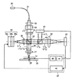
第1実施形態
本実施形態のアライメント装置をこれを用いたアライメント方法について説明する。
図1は、本実施形態に係るアライメント装置の模式構成図である。
本実施形態のアライメント装置においては、電子線近接リソグラフィや等倍X線リソグラフィなどの転写型露光方法において露光するために、ウエハ用アライメントマークが形成され、かつウエハ用アライメントマークの形成面上にレジスト膜が形成されたウエハ22のレジスト膜に対して、等倍露光となる所定の距離をもって、マスク用アライメントマークが形成されたマスク14を位置合わせする。
上記のように位置合わせするために、照明光をウエハの表面に対して斜めに入射させる落射照明系によってウエハ用アライメントマークとマスク用アライメントマークを観察するものであり、ホログラムからなるアライメントマークの再生像はアライメントカメラの物体面に集光する。
【0028】
LEEPL(Low Energy Electron−beam Proximity Projection Lithography)に適用する場合、上記マスクは膜厚0.5μmのメンブレンに対してパターン露光する領域に貫通孔が形成されているステンシルマスクとなる。
ここで、ウエハ22に形成されているウエハ用アライメントマークおよびマスク14に形成されているマスク用アライメントマークは、それぞれホログラムのパターンHGを含み、これらの再生像は、点または線、あるいはこれらの組み合わせである。
【0029】
本実施形態のアライメント装置は、ウエハ22とマスク14の保持部(不図示)、光源30、偏波面保持ファイバ31、コリメータレンズ32、ファラデーアイソレータ33、シリンドリカルレンズ34、ビームスプリッタ35、対物レンズの瞳36、対物レンズ37、結像レンズ38、空間光変調器39、偏光ビームスプリッタ40、第1受光部41、結像レンズ42、第2受光部43、検出部44、保持部位置調整部45および空間フィルタ位置調整部46とを有する。検出部44、保持部位置調整部45および空間フィルタ位置調整部46はコンピュータ47上に実現される。
【0030】
上記の保持部(不図示)は、等倍露光となるように、通常ウエハ22のレジスト膜に対してマスク14を50μm程度の距離に保持するとともに、不図示に機構によりウエハに対するマスクの相対的な位置を調節可能となっている。
【0031】
光源30は、例えば半導体レーザやHe−Neレーザなどの直線偏光レーザであり、ウエハ22に形成されたレジスト膜が感光する領域を除く領域の波長の直線偏光した光である照明光LTI を出射する。
【0032】
光源30からの照明光LTI は、偏波面保持ファイバ31による直線偏光を保持しながらアライメントカメラへと伝送され、コリメータレンズ32により平行光にされ、ファラデーアイソレータ33を経て光源30への戻り光が防止され、シリコンドリカルレンズ34により線型に集光され、ビームスプリッタ35および対物レンズの瞳36を通過して、対物レンズ37により集光され、ウエハの表面に対して斜めの方向からウエハ22のウエハ用アライメントマークおよびマスク14のマスク用アライメントマークに照射される。
【0033】
ウエハ22のウエハ用アライメントマークおよびマスク14のマスク用アライメントマークはホログラムのパターンを含んでおり、あらゆる方向からその反射光を観察できるが、本実施形態の光学系は落射照明系であるので、入射方向に戻って反射する反射光を観察する。
【0034】
ウエハ22のウエハ用アライメントマークおよびマスク14のマスク用アライメントマークにおける反射光は、戻り光LTR として入射経路を辿り、対物レンズ37、対物レンズの瞳36を通過し、ビームスプリッタ35の分光面で進路が分岐され、結像レンズ38により空間光変調器39上に結像する。
空間光変調器39は、例えば液晶部39a、ファイバオプティックプレート39bおよび液晶部39cを重ね合わせた構成となっており、例えば空間フィルタ位置調整部43などの外部から指定された特定の空間周波数領域内の光の偏光を回転させる機能を有する。
本実施形態では、空間フィルタとして、ウエハ22のウエハ用アライメントマークおよびマスク14のマスク用アライメントマークの再生光(以下各アライメントマークの再生光と称する)と、散乱光および高次の光などの再生光以外の光とに空間的に分離して、各アライメントマークの再生光の偏光を90度回転させ、再生光以外の光の偏光は回転させない。
【0035】
空間光変調器39からの戻り光LTR は、結像レンズ38およびビームスプリッタ35を通過し、偏光ビームスプリッタ40に入射する。
ここで、上記の空間光変調器39により指定された空間周波数領域内の光の偏光は90度回転しており、一方、指定以外の領域の光の偏光は回転していないので、偏光ビームスプリッタ40の分光面において、指定された空間周波数領域内の光は反射して進路を屈曲させ、一方、指定以外の領域の光はそのまま透過する。ここでは、偏光ビームスプリッタ40の分光面で反射する光を第1の光LT1、分光面を透過する光を第2の光LT2 とする。
本実施形態においては、上記のように空間光変調器39により各アライメントマークの再生光と再生光以外の光とに分離して前者の偏光を回転させており、第1の光LT1 は各アライメントマークの再生光となり、第2の光LT2 は再生光以外の光となる。
このように、空間光変調器39により特定の空間周波数領域の光の偏光を90度回転させ、この回転させた領域の光を偏光ビームスプリッタ40の分光面で反射し、空間光変調器39で回転させていない領域の光は偏光ビームスプリッタ40を透過させており、空間光変調器39と偏光ビームスプリッタ40により、空間フィルタとしての機能が構成されている。
【0036】
上記の第1の光LT1 である各アライメントマークの再生光は、第1受光部41の受光面上に入射する。一方、第2の光LT2 である再生光以外の光は結像レンズ42により第2受光部43の受光面に結像する。第1受光部41と第2受光部43は、例えば、ともにCCD撮像素子である。
【0037】
上記のように第1受光部41により、ウエハ22のウエハ用アライメントマークとマスク14のマスク用アライメントマークが撮像される。
特に、ウエハ22とマスク14の間隔が50μm程度の距離であるので、ウエハ用アライメントマークの再生光およびマスク用アライメントマークの再生光が第1受光部41受光面の同一面上で結像し、両再生光の干渉縞が生成される。
【0038】
上記の第1受光部41で撮像された干渉縞などの撮像データは、検出部44において画像処理され、ウエハ22のウエハ用アライメントマークとマスク14のマスク用アライメントマークの位置が測定され、マスクとウエハの位置ずれが検出される。さらに、ウエハ用アライメントマークの再生光およびマスク用アライメントマークの再生光の干渉縞などのデータから、ウエハ22とマスク14の間隔を検出する。
次に、保持部(不図示)を位置調整する保持部位置調整部45により、上記のようにして得られたマスクとウエハの位置ずれ、さらにはウエハ22とマスク14の間隔を補正するように、ウエハに対するマスクの位置が調節され、位置合わせされる。
上記の検出部44と保持部位置調整部45は、例えばコンピュータ47上に実現される。
【0039】
上記のアライメント装置において、当初は空間光変調器39により空間的に分離すべき領域の特定、即ち、各アライメントマークの再生光の空間的位置と、再生光以外の光の空間的位置の特定がされていないので、空間光変調器39は両者を分離するように空間周波数領域の指定がされておらず、以下のようにして両者を分離するための空間周波数領域の指定が行われる。
まず、空間光変調器39において、当初は各アライメントマークからの戻り光LTR 全部の偏光を回転させないでおく。
このとき、空間光変調器39からの戻り光LTR は、偏光ビームスプリッタ40に入射しても反射する成分がないため、各アライメントマークの再生光と再生光以外の光を含めて全て透過し、結像レンズ42により第2受光部43に結像する。
【0040】
空間フィルタ位置調整部46において、上記の第2受光部43で撮像されたウエハ用アライメントマークの再生光およびマスク用アライメントマークの再生光と再生光以外の光を含めた全反射光LTR の撮像データの画像処理がなされ、続いてウエハ22のウエハ用アライメントマークの再生光とマスク14のマスク用アライメントマークの再生光の位置が特定され、得られた位置に基づき、各アライメントマークの再生光と再生光以外の光とを空間的に分離して光変調するように、空間光変調器39に出力がなされる。
このとき、第2受光部43においては必ずしも反射光LTR の全てを受光する必要ななく、各アライメントマークの再生光の位置を特定するのに十分な反射光LTR の一部を受光すればよい。
上記のようにして、各アライメントマークの再生光の空間的位置と再生光以外の光の空間的位置の特定がされ、上述のように両者が空間光変調器39と偏光ビームスプリッタ40から構成される空間フィルタにより分離され、スペックルノイズなどの再生光以外の光を除去して各アライメントマークの再生光のみを測定することができる。
上記の空間フィルタ位置調整部46もまた、例えばコンピュータ47上に実現される。
【0041】
上記の本実施形態に係るアライメント装置および方法における線形アライメントマーク再生像以外の形状の再生像を使用する場合には、線形の光束を形成するための上記のシリンドリカルレンズはアライメントマーク再生像の形状に合せた形状の光束を生成するためのホログラム等に置換えてもよい。
マーク像の位置を検出する第2受光部は、CCD撮像素子に代えて、ポジションセンサーダイオードや4分割ディテクタ等の光束位置を測定できるセンサーを使用してもよい。
【0042】
本実施形態では、マスク・ウエハによってアライメントマークの再生像が上記と異なる場合でも、空間光変調器に書込まれる空間フィルタ形状を自由に制御することで対応できる特徴がある。再生像の形状を自由に選択できるので、並進、回転、倍率等の特定のアライメント変数を選択することが可能になる。また、要求されるアライメント精度が得られるように最適な再生像形状を選択し、空間フィルタ形状をそれに合わせることが可能となる。
また、アライメントマーク照明光とアライメントマーク再生光の集光位置が共にアライメント光学系の物体面に重なるようにすることで、光学系の収差による空間フィルタ上の再生光の広がりが小さくなるので、位置合せ精度を向上できる。
また、密着露光においてマスクとウエハ間で両再生光が共通光路とならないために波面歪により発生する誤差を低減し、位置合せ精度を向上できる。
【0043】
本実施形態に係るアライメント装置によれば、電子線近接リソグラフィや等倍X線リソグラフィなどの転写型露光方法におけるウエハやマスクなどのアライメント装置において、アライメントマークとしてホログラフを用いており、位置調整可能な空間フィルタによりスペックルノイズなどの再生光以外の光の影響を除去してアライメントマークの再生光のみを取り出し、高精度にアライメントをすることができる。
【0044】
上記の本実施形態に係るアライメント装置および方法を適用した具体例について説明する。
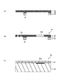
まず、図2(a)に示すように、基板10に酸化シリコン膜11を介してシリコンの薄膜(メンブレン)12を形成し、薄膜領域における基板10と酸化シリコン膜11を除去し、マスクブランクスを形成する。薄膜領域を除く領域において残された基板部分は梁13となって薄膜12を支持する。
【0045】
次に、上記のマスクブランクスの薄膜12上にレジスト膜(不図示)を形成し、X線直接描画露光などでパターン露光する。このとき、マスク用アライメントマークも同時に露光する。マスク用アライメントマークとしては、ホログラムのパターンを含み、これらの再生像は、点または線、あるいはこれらの組み合わせである。
レジスト膜を現像し、これをマスクとしてエッチング処理して、薄膜12にマスク用アライメントマーク12aとパターン12bを形成し、レジスト膜を除去する。
以上のようにして、図2(b)に示すようなLEEPL用のステンシルマスクであるマスク14が形成される。
【0046】
一方、シリコン基板20の表面にパターン加工してウエハ用アライメントマーク20aを形成し、その上層にレジスト膜21を形成する。ウエハ用アライメントマークもまた、マスク用アライメントマークと同様にホログラムのパターンを含むようにする。これらの再生像は、点または線、あるいはこれらの組み合わせである。
以上のようにして、図2(c)に示すような被露光ウエハであるウエハ22が形成される。
【0047】
以降は上述の方法によって行われる。
即ち、図3(a)に示すように、ウエハ22のレジスト膜21とマスク14を所定の距離をもって保持し、レジスト膜が感光する領域を除く領域の波長であって、直線偏光したレーザ光である照明光LTI を、ウエハ22の主面に対して斜めの方向からウエハ22のウエハ用アライメントマーク20aおよびマスク用アライメントマーク12aに対して照射する。
次に、ウエハ用アライメントマーク20aおよびマスク用アライメントマーク12aにおける反射光LTR を受光し、受光した反射光から、光学系に組み込まれた空間フィルタの位置を調整し、ウエハ用アライメントマーク20aおよびマスク用アライメントマーク12aの再生光と、再生光以外の光に分離する。
次に、上記のように分離された再生光を受光して、受光した再生光から、ウエハのアライメントマークに対するマスクのマスク用アライメントマークのずれを検出する。
次に、上記で得られたずれに応じて、ウエハ22に対するマスク14の位置を調節して位置合わせする。
【0048】
上記のアライメントの引き続いて露光を行う場合には、図3(b)に示すように、上記のようにして位置合わせされたマスク14を介してウエハ22に対してレジスト膜が感光する電子線EBなどの露光ビームを照射して露光する。
【0049】
上記の本実施形態に係るアライメント方法および装置で、マスクやウエハに形成するアライメントマークであるホログラムとしては、実際に物体の反射光と参照光を干渉させて形成したホログラムの他、計算機ホログラムを好ましく用いることができる。
例えば、図4の平面図に示すように、点のパターンの集合体であり、各点の間隙がパターン中央部で広く、パターン周辺部で狭くなるようなパターンである。各点の間隙は、ホログラムの再生に用いる光の波長λ程度となっている。
【0050】
第2実施形態
本実施形態は、実質的に第1実施形態と同様のアライメント方法およびアライメント装置であるが、空間フィルタの構成が第1実施形態と異なっている。
図5は、本実施形態に係るアライメント装置の模式構成図である。
本実施形態のアライメント装置は、ウエハ22とマスク14の保持部(不図示)、光源30、偏波面保持ファイバ31、コリメータレンズ32、ファラデーアイソレータ33、シリンドリカルレンズ34、偏光ビームスプリッタ48、1/4波長板49、対物レンズの瞳36、対物レンズ37、1/4波長板50、結像レンズ38、チルトミラー51、スリット(またはピンホール)52、第1受光部53、結像レンズ42、第2受光部43、検出部44、保持部位置調整部45および空間フィルタ位置調整部46とを有する。検出部44、保持部位置調整部45および空間フィルタ位置調整部46はコンピュータ47上に実現される。
【0051】
光源30からの直線偏光したレーザ光である照明光LTI は、偏波面保持ファイバ31による直線偏光を保持しながら伝送され、コリメータレンズ32により平行光にされ、ファラデーアイソレータ33を経て光源30への戻り光が防止され、シリコンドリカルレンズ34により線型に集光され、偏光ビームスプリッタ48を通過し、1/4波長板49により円偏光にされ、対物レンズの瞳36を通過して、対物レンズ37により集光され、ウエハの表面に対して斜めの方向からウエハ22のウエハ用アライメントマークおよびマスク14のマスク用アライメントマークに照射される。
【0052】
ウエハ22のウエハ用アライメントマークおよびマスク14のマスク用アライメントマークはホログラムのパターンを含んでおり、本実施形態においては落射照明系により入射方向に戻って反射する反射光を観察する。
ウエハ22のウエハ用アライメントマークおよびマスク14のマスク用アライメントマークにおける反射光は、戻り光LTR として入射経路を辿り、対物レンズ37、対物レンズの瞳36を通過し、1/4波長板49により直線偏光に戻される。ここで、1/4波長板49を2回通過しているので、戻り光LTR の偏光方向は入射するときから90度直交する方向となっているので、偏光ビームスプリッタ48の分光面で反射して進路が屈曲され、1/4波長板50により再び円偏光にされ、結像レンズ38により集光され、チルトミラー51により反射されてスリット(またはピンホール)52へと進路をとる。チルトミラー51にはガルバノミラーが用いられ、空間フィルタ位置調整部46を実現するコンピュータにより制御される。
【0053】
ここで、結像レンズ38により集光されて結像する位置にスリット(またはピンホール)52が配置されている。スリット(またはピンホール)52を通過する光を第1の光LT1 、スリット(またはピンホール)52を通過せずに表面が鏡面に仕上げられているスリット(またはピンホール)52で反射される光を第2の光LT2 とする。
スリット(またはピンホール)52に対するチルトミラー51の角度が後述の機構により調整されているため、第1の光LT1 はウエハ22のウエハ用アライメントマークおよびマスク14のマスク用アライメントマークの再生光(以下各アライメントマークの再生光と称する)となり、第2の光LT2 は散乱光および高次の光などの再生光以外の光となる。
このように、反射角度を調整できるチルトミラーとスリット(またはピンホール)を組み合わせることで、特定の空間領域の光のみを取り出すことができ、空間フィルタとしての機能が構成されている。
【0054】
上記の第1の光LT1 である各アライメントマークの再生光は、第1受光部53の受光面上に入射する。一方、第2の光LT2 である再生光以外の光は、スリット(またはピンホール)52で反射され、チルトミラー51で反射され、結像レンズ38を通過し、1/4波長板50により再び直線偏光に戻される。ここで、1/4波長板50を2回通過しているので、偏光方向がさらに90度回転され、偏光ビームスプリッタ48の分光面を透過する。その後、結像レンズ42により第2受光部43の受光面に結像する。第1受光部53と第2受光部43は、例えば、ともにCCD撮像素子である。
【0055】
上記のように第1受光部53により、ウエハ22のウエハ用アライメントマークとマスク14のマスク用アライメントマークが撮像され、第1実施形態と同様に、干渉縞などの撮像データが検出部44において画像処理され、ウエハ22のウエハ用アライメントマークとマスク14のマスク用アライメントマークの位置が測定され、マスクとウエハの位置ずれやウエハ22とマスク14の間隔が検出される。
次に、保持部(不図示)を位置調整する保持部位置調整部45により、上記のようにして得られたマスクとウエハの位置ずれ、さらにはウエハ22とマスク14の間隔を補正するように、ウエハに対するマスクの位置が調節され、位置合わせされる。
上記の検出部44と保持部位置調整部45は、例えばコンピュータ47上に実現される。
【0056】
上記のアライメント装置において、当初はチルトミラー51の反射角度が特定されておらず、各アライメントマークの再生光と再生光以外の光を空間的の分離することができておらず、以下のようにして両者を分離するためのチルトミラー51の反射角度が特定される。
まず、スリット(またはピンホール)52の通過領域を限りなくゼロとし、実質的に全反射ミラーとして機能させる。
このとき、チルトミラー51からの戻り光LTR はスリット(またはピンホール)52で各アライメントマークの再生光と再生光以外の光を含めて全て反射し、結像レンズ42により第2受光部43に結像する。
【0057】
空間フィルタ位置調整部46において、上記の第2受光部43で撮像されたウエハ用アライメントマークの再生光およびマスク用アライメントマークの再生光と再生光以外の光を含めた全反射光LTR の撮像データの画像処理がなされ、続いてウエハ22のウエハ用アライメントマークの再生光とマスク14のマスク用アライメントマークの再生光の位置が特定され、得られた位置に基づき、各アライメントマークの再生光と再生光以外の光とを空間的に分離して光変調するように、チルトミラー51に出力がなされ、チルトミラー51の反射角度が決定される。
その後、スリット(またはピンホール)52に所定の通過領域を設けることで、各アライメントマークの再生光のみがスリット(またはピンホール)52を通過し、再生光以外の光はスリット(またはピンホール)52で反射されることになる。
上記のようにして、各アライメントマークの再生光の空間的位置と再生光以外の光の空間的位置の特定がされ、上述のように両者がチルトミラー51とスリット(またはピンホール)52から構成される空間フィルタにより分離され、スペックルノイズなどの再生光以外の光を除去して各アライメントマークの再生光のみを測定することができる。
上記の空間フィルタ位置調整部46もまた、例えばコンピュータ47上に実現される。
【0058】
チルトミラーは、上記ガルバノミラーでなくてもピエゾチルトステアリングミラーであってもよい。あるいはチルトミラーを用いずにスリットをステージで移動してもよい。
また、スリットの面は鏡面でなくても、反射像の強度は低下するが拡散面であってもよい。
再生像を線形にすることによって、マスクとウエハの一方向の相対変位と回転のずれを干渉測定によって高精度に測定できる。
【0059】
本実施形態に係るアライメント装置によれば、電子線近接リソグラフィや等倍X線リソグラフィなどの転写型露光方法におけるウエハやマスクなどのアライメント装置において、アライメントマークとしてホログラフを用いており、位置調整可能な空間フィルタによりスペックルノイズなどの再生光以外の光の影響を除去してアライメントマークの再生光のみを取り出し、高精度にアライメントをすることができる。
【0060】
第3実施形態
図6は、本実施形態に係るアライメント装置の模式構成図である。
本実施形態は、実質的に第1実施形態と同様のアライメント方法およびアライメント装置であるが、ウエハ22のウエハ用アライメントマークおよびマスク14のマスク用アライメントマークはフレネルゾーンプレートZPのパターンを含んでおり、照明光LTI のウエハの表面に対する入射角度が第1実施形態と異なり、ウエハの表面に対して垂直に入射する構成となっている。
【0061】
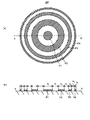
フレネルゾーンプレートZPは、垂直に入射したときのみ、入射経路方向に反射する。従って、落射照明系により観察するためには、ウエハの表面に対する入射角度を垂直とする必要がある。
【0062】
上記の本実施形態に係るアライメント方法および装置で、マスクやウエハに形成するアライメントマークであるフレネルゾーンプレートは、どのような構成でも構わない。例えば、図7(a)の平面図および図7(b)の断面図に示すように、同心円状のリングパターン(P1,P2,P3,P4)の集合体であり、各リングの幅(d1 ,d2 ,d3 ,d4 )および間隔(w1 ,w2 ,w3 )が中央部で広く、パターン周辺部で狭くなるようなパターンである。
【0063】
本実施形態に係るアライメント装置によれば、電子線近接リソグラフィや等倍X線リソグラフィなどの転写型露光方法におけるウエハやマスクなどのアライメント装置において、アライメントマークとしてホログラフを用いており、位置調整可能な空間フィルタによりスペックルノイズなどの再生光以外の光の影響を除去してアライメントマークの再生光のみを取り出し、高精度にアライメントをすることができる。
【0064】
第4実施形態
本実施形態においては、実質的に第2実施形態と同様であるが、第2実施形態のように空間フィルタをアライメントカメラの物体面に共役な位置に置くのではなく、対物レンズの焦点に共役な位置に空間フィルタを置くことが異なる。
但し、ただし、マスクおよびウエハへの照明光と再生光の波面はスリットの長手方向に平行光とする。
このとき、焦点にはスリットと直交する方向の線形スポットが生成されるので、空間フィルタには第2実施形態と直交する方向のスリットを使用すれば良い。
両再生光の干渉縞を測定する第1受光部は、上記実施形態と同様に再生光が発散する位置に置かれ、空間フィルタ位置を制御するための第2受光部は、スリットに共役な位置に置かれる。特に、第1受光部の位置が物体面と共役であるとき収差が最小となり、位置合せ精度が向上する。
【0065】
第5実施形態
本実施形態においては、第1〜第4実施形態のようにアライメントカメラの物体面にフレネルゾーンプレートまたはホログラムの再生像が生成されるのではなく、物体面と異なる面に再生像が生成される。再生像は上記実施形態と同様に点または線、あるいはそれらの組合わせである。
空間フィルタは、再生光が集光する位置、即ち再生像位置に共役な位置に置かれる。
マスクおよびウエハのアライメントマークの再生光の干渉縞を測定して、それらの相対位置を求めるために、第1受光部はアライメントカメラの物体面に共役な位置に置かれる。このため、物体面における干渉縞をアライメントカメラの収差により劣化されずに測定することができるので、位置合せ精度が向上する。
スリット位置を調整するための第2受光部は空間フィルタと共役な位置に置かれる。
【0066】
第6実施形態
上記の第1〜第5実施形態は落射照明系でアライメントマークを観察するものであるが、本実施形態は落射照明系ではなく、特に図示しないが、観察光学系とは別に照明光学系を配置し、観察方向と異なる方向からアライメントマークを照明するものである。
この場合、例えばフレネルゾーンプレートを用いている場合でも、照明光をウエハに垂直な方向から入射させるのではなく、斜めに入射させることができ、電子線などの露光ビーム系の配置を邪魔することがない。
【0067】
第7実施形態
本実施形態は、第1〜第6実施形態に係るアライメント装置を備えた露光装置である。
図8はLEEPLに用いる露光装置の概略図である。
この露光装置は、電子銃60、アパーチャー61、コンデンサレンズ62、一対のメインデフレクター(63,64)および一対の微調整用デフレクター(65,66)を有する。
【0068】
電子銃60から出射された電子ビームEBは、アパーチャー61により径が制限され、コンデンサレンズ62により平行なビームにされる。
メインデフレクター(63,64)は、電子ビームEBが平行なままマスク14に垂直に入射するように、電子ビームEBを偏向させる。
電子ビームEBはラスターまたはベクトル走査モードのいずれかでステンシルマスク14に入射するが、いずれの場合も電子ビームEBの偏向にメインデフレクター(63,64)が用いられる。微調整用デフレクター(65,66)はメインデフレクター(63,64)によって偏向された電子ビームEBをさらに微調整する。
ステンシルマスク47を透過した電子ビームEBは、ウエハ22に形成された電子線露光用のレジスト膜に照射され、パターン露光される。
【0069】
ここで、本実施形態に係る露光装置はアライメント装置70を備えている。
このアライメント装置70は、第1〜第6実施形態に係るアライメント装置と同様の構成である。
即ち、照明光LTI がウエハ22のアライメントマークおよびマスク14のマスク用アライメントマークに対して照射される。
さらに、アライメントマークおよびマスク14のマスク用アライメントマークにおける反射光が受光され、受光された反射光から、各アライメントマークの再生光のみが空間フィルタにより分離され、各アライメントマークの再生光が受光され、ウエハ22のアライメントマークに対するマスク14のアライメントマークのずれが検出され、このずれに応じて、ウエハ22に対するマスク14の位置が調節されて位置合わせされる。
本実施形態の露光装置は、上記のようにウエハ22に対するマスク14の位置を高精度に合わせた後、露光と行うことができる。
図面上、照明光がウエハに対して斜めに入射する場合を示しているが、ウエハに対して垂直に入射する構成とすることも可能である。
【0070】
本実施形態のアライメント方法および装置、あるいは露光装置は、以下のような利点を有する。
1.フレネルゾーンプレートの照明光スペクトルを広帯域化しないため高解像な再生像が得られるので、位置合せ精度が向上する。空間光変調器を使用するため空間フィルタ形状、位置を調整できるので、ゾーンプレート再生像の形状に最適な空間フィルタを容易に構成でき、高速に空間フィルタ位置を調整できる。
2.アライメントマークを構成するフレネルゾーンプレートは、要素ドットの面密度がLEEPLで使用されているアライメントマークの面密度よりも高いので、マーク形状歪による誤差を平均化により低減できる。従って、高精度な位置合せが可能となる。
3.従来のマスクおよびウエハ上のアライメントマークを結像する斜方観察方式では、アライメント光学系の焦点深度内の狭い範囲のアライメントマークしか観察できなかったので、アライメントマークを多数配置しても一度に観察できるアライメントマークの個数には制限があった。しかし、フレネルゾーンプレートは焦点深度外も含めた全領域の要素ドットによる回折光が干渉することによって再生像が生成されるので、平均化される要素ドット数が遥かに多くなる。従って、平均化により測定精度が向上する。
4.フレネルゾーンプレートやホログラムはコヒーレント光の重ね合わせのため、再生像の明るさが要素ドット数の2乗に比例して向上するので、薄いレジスト等に記録されたアライメントマークであっても十分な明るさのマーク像が得られる。
5.従来のマスクおよびウエハ上のアライメントマークを結像する斜方観察方式では、一つの光学系によって一方向の位置ずれしか検出できないが、ホログラムを用いることによって2方向と回転、倍率の位置ずれを同時に検出できる。さらに、ホログラムを使用する場合には、マスクとウエハの間の間隔と傾き角も測定できる。
6.マスクおよびウエハの両再生光の干渉縞を測定する光波干渉計を構成できるので、高精度な位置合せが可能である。
7.特に、マスクとウエハを近接させる密着露光ではフィゾー干渉計を構成できるので、高精度な光学系が必要ない。従って、対物レンズの作動距離等に対する制約が緩和され、光学系のレイアウトの自由度が増大するので、マスクに照射される電子線などによるスペース的な制約が大きい電子線密着露光等においてアライメント光学系のレイアウトが容易になる。また、高価な対物レンズ等が必要なくなる。
8.従来のマスクおよびウエハ上のアライメントマークを結像する斜方観察方式では、両アライメントマークのフォーカス位置の間隔を測定することによって、マスクとウエハの間隔を測定しているため、測定精度はアライメント光学系の焦点深度程度になる。本発明では、マスクとウエハの両再生像の干渉縞を測定することによってマスクとウエハの間隔を測定できるので、レーザ光の波長以下の測定精度を容易に得ることができる。従って、斜方観察方式よりもマスクとウエハの間隔を高精度に調整できる。
【0071】
以上、フレネルゾーンプレートとホログラムを適宜に用いて説明したが、フレネルゾーンプレートとホログラムは原理、効果等に類似点が多いので、両者を置換えて使用しても問題はない。
【0072】
本発明のアライメント方法、アライメント装置および露光装置は、上記の実施形態に限定されない。
例えば、本実施形態においては、ステンシルマスクのアライメント方法について説明したが、各種論文および特許により公知となっているマスク製造プロセスを適用することにより、各次世代露光技術用のマスクのアライメント方法に適用できる。
また、本発明のアライメント方法および装置は、被露光ウエハにパターン露光する工程を有する半導体装置の製造方法において、パターン露光するためのマスクをアライメントする方法や装置として適用できる。
その他、本発明の要旨を逸脱しない範囲で種々の変更が可能である。
【0073】
【発明の効果】
本発明のアライメント方法によれば、電子線近接リソグラフィや等倍X線リソグラフィなどの転写型露光方法におけるウエハやマスクなどのアライメント装置において、アライメントマークとしてホログラフを用いており、位置調整可能な空間フィルタによりスペックルノイズなどの再生光以外の光の影響を除去してアライメントマークの再生光のみを取り出し、高精度にアライメントをすることができる。
【0074】
本発明のアライメント装置によれば、電子線近接リソグラフィや等倍X線リソグラフィなどの転写型露光方法におけるウエハやマスクなどのアライメント装置において、アライメントマークとしてホログラフを用いており、位置調整可能な空間フィルタによりスペックルノイズなどの再生光以外の光の影響を除去してアライメントマークの再生光のみを取り出し、高精度にアライメントをすることができる。
【0075】
本発明の露光装置によれば、本発明のアライメント装置により高精度にウエハに対するマスクの位置を高精度に合わせた後、露光と行うことができる。
【0076】
本発明の半導体装置の製造方法によれば、本発明のアライメント装置により高精度にウエハに対するマスクの位置を高精度に合わせて露光し、半導体装置を製造することができる。
【図面の簡単な説明】
【図1】図1は第1実施形態に係るアライメント装置の模式構成図である。
【図2】図2(a)〜(c)は第1実施形態に係るアライメント方法の工程を示す断面図である。
【図3】図3(a)および(b)は第1実施形態に係るアライメント方法の工程を示す断面図である。
【図4】図4は第1実施形態において用いるホログラム例の平面図である。
【図5】図5は第2実施形態に係るアライメント装置の模式構成図である。
【図6】図6は第3実施形態に係るアライメント装置の模式構成図である。
【図7】図7は第3実施形態において用いるフレネルゾーンプレート例の平面図である。
【図8】図8は第7実施形態に係る露光装置の模式構成図である。
【符号の説明】
10…基板、11…酸化シリコン膜、12…薄膜(メンブレン)、13…梁、14…マスク、20…シリコン基板、21…レジスト膜、22…ウエハ、30…光源、31…偏波面保持ファイバ、32…コリメータレンズ、33…ファラデーアイソレータ、34…シリンドリカルレンズ、35…ビームスプリッタ、36…対物レンズの瞳、37…対物レンズ、38…結像レンズ、39…空間光変調器、40…偏光ビームスプリッタ、41…第1受光部、42…結像レンズ、43…第2受光部、44…検出部、45…保持部位置調整部、46…空間フィルタ位置調整部、47…コンピュータ、48…偏光ビームスプリッタ、49…1/4波長板、50…1/4波長板、51…チルトミラー、52…スリット(またはピンホール)、53…第1受光部、60…電子銃、61…アパーチャー、62…コンデンサレンズ、63,64…一対のメインデフレクター、65,66…一対の微調整用デフレクター、70…アライメント装置、LTI …照明光、LTR …反射光、LT1 …第1の光、LT2 …第2の光。[0001]
TECHNICAL FIELD OF THE INVENTION
The present invention relates to an alignment method and an alignment apparatus for a mask used in a lithography process for manufacturing a semiconductor device, and an exposure apparatus and a semiconductor device manufacturing method using the same.
[0002]
[Prior art]
As a next-generation exposure technology that replaces photolithography, transfer-type exposure methods, such as electron beam proximity lithography and 1: 1 X-ray lithography, have been developed in which a mask is brought close to the wafer to be exposed using electron beams or X-rays. ing.
A mask used in these lithography is composed of a 0.5 μm-thick Si film, a SiC film, or a thin film such as diamond.
[0003]
In the next-generation exposure technology described above, for example, an alignment device that measures and positions the relative position between the mask and the wafer to be exposed in real time is used.
For example, long-wavelength light that does not expose the resist film formed on the wafer to be exposed is used, and alignment marks written on the mask and the wafer are irradiated with measurement light (illumination light). The light that is scattered and returned is detected to form an image on the image sensor, image processing is performed, the position of the alignment mark is measured, and the positional deviation between the mask and the wafer is detected.
The position of the mask with respect to the wafer is adjusted and adjusted so as to correct the misalignment between the mask and the wafer obtained as described above.
[0004]
For example, in an exposure method described in Patent Document 1, a method of obtaining a best focus position of a projection optical system is described.
According to this method, a latent image pattern of a focus measurement mark is exposed by changing a focus position with respect to a projection optical system in a peripheral unexposed area on a wafer on which a resist film is formed, and is exposed in a direction oblique to the latent image pattern. , And the intensity of the interference light of a set of diffracted light generated in parallel from the latent image pattern is obtained, and the focus position where the intensity of the interference light is maximized is determined as the best focus position.
[0005]
The alignment method using a hologram or a Fresnel zone plate, which is one of the alignment methods as described above, is characterized in that alignment can be performed with high accuracy without being affected by the shape distortion of the alignment pattern, as compared with a method using a simple alignment pattern. There is.
When performing relative positioning between a mask and a wafer using a hologram or a Fresnel zone plate, a coherent laser is used as a light source.
[0006]
In particular, in a system in which an alignment mark on a wafer is imaged through a mask by an epi-illumination oblique observation optical system in EB contact exposure (LEEEPL), the intensity of scattered light due to the alignment mark on the wafer is small, so that the resist on the wafer is removed. In the case of coating, etc., the mark image may be darkened and the alignment accuracy may be reduced, but a hologram or a Fresnel zone plate can obtain a bright reproduced image due to interference of scattered light from element dots constituting the hologram and the Fresnel zone plate. .
[0007]
However, when a laser beam illuminates an alignment mark on a mask or a wafer, scattered light or higher-order diffracted light from an alignment pattern between the mask and the wafer interferes with the speckle noise on the sensor surface. Therefore, the noise of the output signal from the sensor increases, and the positioning accuracy decreases. In particular, zone plates and holograms on a wafer or mask formed of a binary pattern have a large amount of high-order diffracted light, so that noise is increased and measurement errors are increased.
Also, in proximity exposure using an electron beam (EB) or X-ray with a mask and a wafer brought close to each other, speckle noise is generated due to interference of illumination light and reproduction light reflected multiple between the mask and the wafer. Occurs, and the alignment accuracy decreases.
[0008]
Further, there is an interferometer as a highly accurate optical applied measurement method. The reproduced images of the alignment marks on the mask and the wafer are caused to interfere with each other, and the relative displacement between the alignment marks can be measured from the number of interference fringes.
Furthermore, if the phase of the interference fringes is measured by the sub-fringe method based on the shift of the relative position of the mask and the wafer or the wavelength shift of the laser beam, the relative position of the mask and the wafer can be determined even if the number of interference fringes is one or less. It can measure with high accuracy.
However, illuminating the zone plate or the hologram with the laser light as described above causes speckle noise, which lowers the alignment accuracy.
[0009]
As a countermeasure against the above speckle noise, for example, in Patent Document 2, the coherency of a light source is reduced by controlling a drive current value of a semiconductor laser and using a superluminescent diode.
In addition, a spatial filter is effective for removing speckle noise from a reproduced image of a Fresnel zone plate or a hologram.
[0010]
[Patent Document 1]
JP-A-6-267824
[Patent Document 2]
Japanese Patent No. 2827312
[0011]
[Problems to be solved by the invention]
However, if the coherency is reduced, the reproduced image of the hologram or Fresnel zone plate will be blurred due to chromatic dispersion. For this reason, the spot diameter does not become sufficiently small on the sensor, so that the positioning accuracy decreases.
[0012]
Furthermore, when a spatial filter is used, not only the position of the mark reconstructed image but also the direction of the reconstructed light changes depending on the displacement of the mask and the wafer. Therefore, the spatial filter must be moved according to the position of the mask and the wafer. However, it takes time to adjust the position of the spatial filter, which causes a decrease in the throughput of the exposure apparatus.
[0013]
The present invention has been made in view of the above-described problems, and accordingly, the present invention provides an alignment method and apparatus for a wafer or a mask in a transfer exposure method such as electron beam proximity lithography or 1: 1 X-ray lithography. It is an object of the present invention to provide an alignment method and an alignment apparatus capable of removing an influence of speckle noise and performing high-accuracy alignment when a holographic or Fresnel zone pattern is used as a mark, and an exposure apparatus and a semiconductor device manufacturing method using the same. And
[0014]
[Means for Solving the Problems]
In order to achieve the above object, a mask alignment method according to the present invention is an alignment method for aligning an alignment target on which an alignment mark including a hologram pattern or a Fresnel zone plate pattern is formed, wherein a laser beam is emitted. Irradiating the alignment mark, receiving at least a part of the laser beam reflected by the alignment mark, and adjusting a position of the spatial light according to at least a part of the received reflected light. A step of separating the reproduction light of the alignment mark into light other than the reproduction light, a step of receiving the reproduction light, and detecting a displacement of the position of the alignment object from the received reproduction light. And adjusting the position of the alignment object according to the displacement. And a step of aligning.
[0015]
In the mask alignment method of the present invention described above, first, a laser beam is applied to an alignment mark of an alignment target, which is a hologram or a Fresnel zone plate, and at least a part of the reflected light of the laser beam at the alignment mark at this time. Is received.
Next, according to at least a part of the received reflected light, the alignment mark is separated into reproduction light and light other than the reproduction light.
Next, the reproduction light of the alignment mark is received, and the displacement of the position of the alignment target is detected from the received reproduction light of the alignment mark.
Next, the position of the alignment target is adjusted and aligned according to the deviation obtained above.
[0016]
In order to achieve the above object, a mask alignment method according to the present invention is configured such that a wafer alignment mark including a hologram pattern or a Fresnel zone plate pattern is formed, and a resist is formed on a surface on which the wafer alignment mark is formed. An alignment method for aligning a mask on which a mask alignment mark including a hologram pattern or a Fresnel zone plate pattern is formed at a predetermined distance for equal exposure with respect to the resist film of a wafer on which a film is formed. A step of holding the wafer and the mask such that a distance between the resist film and the mask of the wafer is substantially the predetermined distance; and a laser having a wavelength in a region excluding a region where the resist film is exposed. Light is applied to the wafer alignment mark of the wafer. And irradiating the mask alignment mark of the mask with light, receiving at least a part of the reflected light of the laser light on the wafer alignment mark and the mask alignment mark, A step of separating the wafer alignment mark and the mask alignment mark into reproduction light and light other than the reproduction light by a position-adjustable spatial filter according to at least a part thereof; and receiving the reproduction light. Detecting the displacement of the mask alignment mark of the mask with respect to the alignment mark of the wafer from the received reproduction light, and adjusting the position of the mask with respect to the wafer according to the displacement. Positioning step.
[0017]
In the mask alignment method of the present invention described above, first, the wafer and the mask are held so that the distance between the resist film and the mask on the wafer is substantially a predetermined distance, and the wavelength of the region excluding the region where the resist film is exposed is adjusted. A laser beam is applied to a wafer alignment mark of a wafer, which is a hologram or a Fresnel zone plate, and a mask alignment mark of a mask, and at least the reflected light of the laser light at the wafer alignment mark and the mask alignment mark at this time. Partially received light.
Next, according to at least a part of the received reflected light, the light is separated into reproduction light of the wafer alignment mark and the mask alignment mark and light other than the reproduction light.
Next, the reproduction light is received, and a shift of the mask alignment mark of the mask with respect to the alignment mark of the wafer is detected from the received reproduction light.
Next, the position of the mask with respect to the wafer is adjusted and adjusted according to the shift obtained above.
[0018]
In order to achieve the above object, the mask alignment apparatus of the present invention is an alignment apparatus for aligning an alignment target on which an alignment mark including a hologram pattern or a Fresnel zone plate pattern is formed, A holding unit for holding the alignment object, a light source that emits laser light, a first light receiving unit, a second light receiving unit, and irradiating the laser light to an alignment mark of the alignment object, A spatial filter capable of separating and adjusting the position of laser light reflected by the alignment mark into reproduction light of the alignment mark and light other than the reproduction light, and coupling the reproduction light to the first light receiving unit; An optical system for coupling at least a part of the reflected light to the second light receiving unit; A spatial filter position adjusting unit that adjusts a position of the spatial filter so as to separate the reproduction light and light other than the reproduction light according to at least a part of the reflected light received by the unit; A detecting unit that detects a positional shift of the alignment target from the reproduction light received by the first light receiving unit; and a holding unit position adjustment that adjusts a position of the alignment target by the holding unit in accordance with the shift. And a part.
[0019]
In the mask alignment apparatus of the present invention, the optical system irradiates the laser beam from the light source to the alignment mark of the alignment target, which is a hologram or a Fresnel zone plate, and the obtained reflected light is included in the optical system. The alignment mark is separated into reproduction light and light other than the reproduction light of the alignment mark by a spatial filter whose position can be adjusted and coupled to the first light receiving portion, and at least a part of the reflected light is coupled to the second light receiving portion. .
At this time, the position of the spatial filter is adjusted by the spatial filter position adjusting unit so as to separate the alignment mark into reproduction light and light other than the reproduction light in accordance with at least a part of the reflected light.
As a result, only the reproduction light of the alignment mark separated as described above is received by the first light receiving unit, and the position deviation of the alignment object is detected by the detection unit from the reproduction light of the alignment mark, and the obtained deviation is obtained. The position of the alignment target by the holding unit is adjusted by the holding unit position adjusting unit in accordance with.
[0020]
In order to achieve the above object, a mask alignment apparatus according to the present invention is configured such that a wafer alignment mark including a hologram pattern or a Fresnel zone plate pattern is formed, and a resist is formed on a surface on which the wafer alignment mark is formed. An alignment apparatus for aligning a mask on which a mask alignment mark including a hologram pattern or a Fresnel zone plate pattern is formed at a predetermined distance for equal exposure with respect to the resist film on a wafer on which a film is formed. A holding unit for holding the wafer and the mask such that a distance between the resist film of the wafer and the mask is substantially the predetermined distance; a light source for emitting laser light; and a first light receiving unit A second light receiving unit; Irradiating the laser beam with respect to the wafer alignment mark and the mask alignment mark, and reproducing the mask alignment mark and the mask alignment mark of the mask. A spatial filter that is separable and position-adjustable into light and light other than the reproduction light, couples the reproduction light to the first light receiving unit, and transmits at least a part of the reflected light to the second light reception unit And a position of the spatial filter so as to separate the reproduction light and the light other than the reproduction light according to at least a part of the reflected light received by the second light receiving unit. And a spatial filter position adjusting unit for adjusting the position of the wafer, from the reproduction light received by the second light receiving unit, Has a detecting unit for detecting a deviation of the alignment mark for a mask of the mask with respect to serial alignment mark, according to the deviation, and a holding portion position adjusting unit for adjusting a position of the mask relative to the wafer by the holder.
[0021]
The mask alignment apparatus of the present invention irradiates a laser beam from a light source to an alignment mark for a wafer, which is a hologram or a Fresnel zone plate, and a mask alignment mark for a mask by an optical system. The light is separated into light other than the reproduction light and the reproduction light of the alignment mark for the wafer and the alignment mark for the mask by the position adjustable spatial filter included in the optical system, and the reproduction light is coupled to the first light receiving unit. Further, at least a part of the reflected light is coupled to the second light receiving unit.
The spatial filter position adjuster adjusts the position of the spatial filter so as to separate the reproduced light from the wafer alignment mark and the mask alignment mark into light other than the reproduced light according to at least a part of the reflected light at this time. I do.
As a result, only the reproduction light of the alignment mark separated as described above is received by the first light receiving unit, and the position deviation between the mask and the wafer is detected by the detection unit from the reproduction light of the wafer alignment mark and the mask alignment mark. The position of the mask with respect to the wafer by the holder is detected and adjusted by the holder adjuster in accordance with the detected deviation.
[0022]
In order to achieve the above object, the exposure apparatus of the present invention is configured such that a wafer alignment mark including a hologram pattern or a Fresnel zone plate pattern is formed, and a resist film is formed on a surface on which the wafer alignment mark is formed. An alignment unit is provided for aligning a mask on which a mask alignment mark including a hologram pattern or a Fresnel zone plate pattern is formed at a predetermined distance for equal exposure with respect to the resist film of the formed wafer. An exposure apparatus that performs exposure with a predetermined exposure beam, wherein the alignment unit holds the wafer and the mask such that a distance between a resist film of the wafer and the mask is substantially the predetermined distance. A light source that emits laser light, a first light receiving unit, and a second light receiving unit. A light section, and irradiating the laser light to the wafer alignment mark of the wafer and the mask alignment mark of the mask, and reflecting the laser light reflected by the wafer alignment mark and the mask alignment mark to the mask. A spatial filter that is separable and position-adjustable to a reproduction light of the mask alignment mark and the mask alignment mark and a light other than the reproduction light, and couples the reproduction light to the first light receiving unit; An optical system that couples at least a part of the reflected light to the second light receiving unit;
Spatial filter position adjustment for adjusting the position of the spatial filter so as to separate the reproduction light and light other than the reproduction light according to at least a part of the reflected light received by the second light receiving unit. A detecting unit configured to detect a shift of the mask alignment mark of the mask with respect to the alignment mark of the wafer from the reproduction light received by the second light receiving unit; And a holding section position adjusting section for adjusting the position of the mask with respect to the wafer by the section.
[0023]
The exposure apparatus of the present invention includes the alignment apparatus of the present invention as an alignment unit for aligning a wafer alignment mark of a wafer and a mask alignment mark of a mask, and performs exposure with a predetermined exposure beam. It is.
[0024]
In order to achieve the above object, a method of manufacturing a semiconductor device according to the present invention, wherein a wafer alignment mark including a hologram pattern or a Fresnel zone plate pattern is formed, and the wafer alignment mark is formed on a surface on which the wafer alignment mark is formed. A method for manufacturing a semiconductor device, comprising a step of pattern-exposing a wafer having a resist film formed thereon, using a mask having a predetermined pattern formed with a mask alignment mark including a hologram pattern or a Fresnel zone plate pattern, A step of holding the wafer and the mask such that the distance between the resist film and the mask of the wafer is substantially the predetermined distance, and laser light having a wavelength in a region excluding a region where the resist film is exposed, Wafer alignment mark for the wafer and mask for the mask Irradiating the laser beam with respect to the alignment mark, receiving at least a part of the reflected light of the laser light in the wafer alignment mark and the mask alignment mark, and responding to at least a part of the received reflected light. A step of separating the reproduction light of the wafer alignment mark and the mask alignment mark into light other than the reproduction light, a step of receiving the reproduction light, and a step of receiving the reproduction light. Detecting, from the reproduction light, a shift of the mask alignment mark of the mask with respect to the alignment mark of the wafer, and adjusting the position of the mask with respect to the wafer in accordance with the shift to perform alignment; Before the wafer through the aligned mask Resist film and a step of exposing by irradiating an exposure beam that is sensitive.
[0025]
In the method for manufacturing a semiconductor device according to the present invention, the resist film is exposed to the wafer through the aligned mask after adjusting and positioning the position of the mask with respect to the wafer by the alignment method of the present invention. Exposure is performed by irradiating an exposure beam.
[0026]
BEST MODE FOR CARRYING OUT THE INVENTION
Hereinafter, an embodiment of a mask alignment method and a mask alignment apparatus according to the present embodiment and an exposure apparatus including the above-described alignment apparatus will be described with reference to the drawings.
[0027]
First embodiment
An alignment method using the alignment apparatus of the present embodiment will be described.
FIG. 1 is a schematic configuration diagram of an alignment apparatus according to the present embodiment.
In the alignment apparatus of the present embodiment, in order to perform exposure in a transfer exposure method such as electron beam proximity lithography or equal-size X-ray lithography, a wafer alignment mark is formed, and a resist is formed on a surface on which the wafer alignment mark is formed. With respect to the resist film on the
In order to perform alignment as described above, the epi-illumination system in which illumination light is obliquely incident on the surface of the wafer is used to observe the wafer alignment mark and the mask alignment mark. The image is focused on the object plane of the alignment camera.
[0028]
When applied to LEEPL (Low Energy Electron-Beam Proximity Projection Lithography), the mask is a stencil mask in which a through hole is formed in a region where a 0.5 μm-thick membrane is subjected to pattern exposure.
Here, the wafer alignment mark formed on the
[0029]
The alignment apparatus according to the present embodiment includes a holder (not shown) for holding the
[0030]
The holding unit (not shown) holds the
[0031]
The
[0032]
Illumination light LT from
[0033]
The wafer alignment mark of the
[0034]
The reflected light at the wafer alignment mark of the
The spatial
In the present embodiment, as spatial filters, reproduction light of a wafer alignment mark of the
[0035]
Return light LT from spatial
Here, the polarization of the light in the spatial frequency region designated by the spatial
In the present embodiment, as described above, the spatial
In this way, the spatial
[0036]
The above first light LT1 The reproduction light of each alignment mark is incident on the light receiving surface of the first
[0037]
As described above, the first
In particular, since the distance between the
[0038]
Image data such as interference fringes captured by the first
Next, the holding unit
The
[0039]
In the above-described alignment apparatus, at first, the area to be spatially separated by the spatial
First, the spatial
At this time, the return light LT from the spatial
[0040]
In the spatial filter
At this time, the reflected light LT is not necessarilyR Is sufficient to specify the position of the reproduction light of each alignment mark without having to receive allR May be partially received.
As described above, the spatial position of the reproduction light and the spatial position of light other than the reproduction light of each alignment mark are specified. As described above, both of them are constituted by the spatial
The spatial filter
[0041]
When using a reconstructed image having a shape other than the linear alignment mark reconstructed image in the alignment apparatus and method according to the above-described embodiment, the cylindrical lens for forming a linear light beam has the shape of the alignment mark reconstructed image. It may be replaced with a hologram or the like for generating a light beam having a combined shape.
The second light receiving unit that detects the position of the mark image may use a sensor that can measure the position of the light beam, such as a position sensor diode or a quadrant detector, instead of the CCD image sensor.
[0042]
This embodiment is characterized in that even if the reproduced image of the alignment mark differs from the above due to the mask / wafer, it can be handled by freely controlling the shape of the spatial filter written in the spatial light modulator. Since the shape of the reproduced image can be freely selected, specific alignment variables such as translation, rotation, and magnification can be selected. In addition, it is possible to select an optimum reproduced image shape so as to obtain the required alignment accuracy, and to match the shape of the spatial filter.
Also, by making the converging positions of the alignment mark illumination light and the alignment mark reproduction light both overlap the object plane of the alignment optical system, the spread of the reproduction light on the spatial filter due to the aberration of the optical system is reduced. The alignment accuracy can be improved.
In addition, since both reproduction lights do not have a common optical path between the mask and the wafer in the contact exposure, errors caused by wavefront distortion can be reduced, and alignment accuracy can be improved.
[0043]
According to the alignment apparatus according to the present embodiment, a holographic is used as an alignment mark in an alignment apparatus such as a wafer or a mask in a transfer type exposure method such as electron beam proximity lithography or 1: 1 X-ray lithography, and the position can be adjusted. The spatial filter removes the influence of light other than the reproduction light, such as speckle noise, and extracts only the reproduction light of the alignment mark to perform alignment with high accuracy.
[0044]
A specific example to which the above-described alignment apparatus and method according to the present embodiment are applied will be described.
First, as shown in FIG. 2A, a silicon thin film (membrane) 12 is formed on a
[0045]
Next, a resist film (not shown) is formed on the
The resist film is developed and etched using the resist film as a mask to form a
As described above, the
[0046]
On the other hand, pattern processing is performed on the surface of the
As described above, the
[0047]
Thereafter, the above-described method is used.
That is, as shown in FIG. 3A, the resist
Next, reflected light LT at
Next, the reproduction light separated as described above is received, and a deviation of the mask alignment mark of the mask with respect to the alignment mark of the wafer is detected from the received reproduction light.
Next, the position of the
[0048]
When exposure is performed subsequent to the above-described alignment, as shown in FIG. 3B, the electron beam EB in which the resist film is exposed to the
[0049]
In the above-described alignment method and apparatus according to the present embodiment, the hologram that is an alignment mark formed on a mask or a wafer is preferably a computer generated hologram, in addition to a hologram formed by actually interfering reflected light and reference light of an object. Can be used.
For example, as shown in the plan view of FIG. 4, the pattern is an aggregate of point patterns, and the gap between the points is wide at the center of the pattern and narrow at the periphery of the pattern. The gap between each point is about the wavelength λ of light used for reproducing the hologram.
[0050]
Second embodiment
This embodiment is substantially the same alignment method and alignment apparatus as the first embodiment, but differs from the first embodiment in the configuration of the spatial filter.
FIG. 5 is a schematic configuration diagram of the alignment apparatus according to the present embodiment.
The alignment apparatus according to the present embodiment includes a holder (not shown) for holding the
[0051]
Illumination light LT which is linearly polarized laser light from the
[0052]
The wafer alignment mark of the
The reflected light at the wafer alignment mark of the
[0053]
Here, a slit (or pinhole) 52 is arranged at a position where the light is condensed by the
Since the angle of the
As described above, by combining the tilt mirror and the slit (or pinhole) that can adjust the reflection angle, it is possible to extract only light in a specific spatial region, and a function as a spatial filter is configured.
[0054]
The above first light LT1 The reproduction light of each alignment mark is incident on the light receiving surface of the first
[0055]
As described above, the first
Next, the holding unit
The
[0056]
In the above alignment device, the reflection angle of the
First, the passing area of the slit (or pinhole) 52 is set to zero as much as possible, so that the slit (or pinhole) 52 functions substantially as a total reflection mirror.
At this time, the return light LT from the
[0057]
In the spatial filter
After that, by providing a predetermined passage area in the slit (or pinhole) 52, only the reproduction light of each alignment mark passes through the slit (or pinhole) 52, and light other than the reproduction light passes through the slit (or pinhole). It will be reflected at 52.
As described above, the spatial position of the reproduction light and the spatial position of the light other than the reproduction light of each alignment mark are specified. As described above, both are composed of the
The spatial filter
[0058]
The tilt mirror may be a piezo tilt steering mirror instead of the galvanometer mirror. Alternatively, the slit may be moved on the stage without using the tilt mirror.
Also, the surface of the slit may not be a mirror surface, but may be a diffusion surface although the intensity of the reflected image is reduced.
By making the reconstructed image linear, it is possible to measure the relative displacement and rotational deviation of the mask and the wafer in one direction with high accuracy by interference measurement.
[0059]
According to the alignment apparatus according to the present embodiment, a holographic is used as an alignment mark in an alignment apparatus such as a wafer or a mask in a transfer type exposure method such as electron beam proximity lithography or 1: 1 X-ray lithography, and the position can be adjusted. The spatial filter removes the influence of light other than the reproduction light, such as speckle noise, and extracts only the reproduction light of the alignment mark to perform alignment with high accuracy.
[0060]
Third embodiment
FIG. 6 is a schematic configuration diagram of the alignment apparatus according to the present embodiment.
The present embodiment is an alignment method and an alignment apparatus substantially similar to those of the first embodiment, but the alignment mark for the
[0061]
The Fresnel zone plate ZP reflects in the direction of the incident path only when vertically incident. Therefore, in order to observe with the epi-illumination system, it is necessary to make the incident angle with respect to the surface of the wafer perpendicular.
[0062]
In the above-described alignment method and apparatus according to the present embodiment, the Fresnel zone plate, which is an alignment mark formed on a mask or a wafer, may have any configuration. For example, as shown in the plan view of FIG. 7A and the cross-sectional view of FIG. 7B, it is an aggregate of concentric ring patterns (P1, P2, P3, P4), and the width of each ring (d1 , D2 , D3 , D4 ) And spacing (w1 , W2 , W3 Is a pattern that is wide at the center and narrow at the periphery of the pattern.
[0063]
According to the alignment apparatus according to the present embodiment, a holographic is used as an alignment mark in an alignment apparatus such as a wafer or a mask in a transfer type exposure method such as electron beam proximity lithography or 1: 1 X-ray lithography, and the position can be adjusted. The spatial filter removes the influence of light other than the reproduction light, such as speckle noise, and extracts only the reproduction light of the alignment mark, thereby enabling highly accurate alignment.
[0064]
Fourth embodiment
This embodiment is substantially the same as the second embodiment except that the spatial filter is not placed at a position conjugate to the object plane of the alignment camera as in the second embodiment, but is conjugated to the focal point of the objective lens. It is different to place a spatial filter at a suitable position.
However, the wavefronts of the illumination light and the reproduction light for the mask and the wafer are parallel to the longitudinal direction of the slit.
At this time, since a linear spot in the direction orthogonal to the slit is generated at the focal point, a slit in the direction orthogonal to the second embodiment may be used for the spatial filter.
The first light receiving section for measuring the interference fringes of both reproduction lights is placed at the position where the reproduction light diverges as in the above embodiment, and the second light receiving section for controlling the spatial filter position is located at a position conjugate to the slit. To be placed. In particular, when the position of the first light receiving unit is conjugate with the object plane, the aberration is minimized, and the alignment accuracy is improved.
[0065]
Fifth embodiment
In the present embodiment, a reproduced image of a Fresnel zone plate or a hologram is not generated on the object plane of the alignment camera as in the first to fourth embodiments, but a reproduced image is generated on a plane different from the object plane. . The reproduced image is a point or a line, or a combination thereof, as in the above embodiment.
The spatial filter is placed at a position where the reproduction light is focused, that is, a position conjugate to the reproduction image position.
The first light receiving unit is placed at a position conjugate to the object plane of the alignment camera in order to measure interference fringes of the reproduction light of the alignment marks on the mask and the wafer and determine their relative positions. Therefore, the interference fringes on the object surface can be measured without being deteriorated by the aberration of the alignment camera, and the alignment accuracy is improved.
The second light receiving unit for adjusting the slit position is placed at a position conjugate with the spatial filter.
[0066]
Sixth embodiment
Although the above-described first to fifth embodiments are for observing the alignment mark with an epi-illumination system, the present embodiment is not an epi-illumination system, and although not shown, an illumination optical system is arranged separately from the observation optical system. Then, the alignment mark is illuminated from a direction different from the observation direction.
In this case, for example, even when a Fresnel zone plate is used, the illumination light can be obliquely incident on the wafer instead of being incident on the wafer in a direction perpendicular to the wafer, which hinders the arrangement of an exposure beam system such as an electron beam. There is no.
[0067]
Seventh embodiment
This embodiment is an exposure apparatus provided with the alignment apparatus according to the first to sixth embodiments.
FIG. 8 is a schematic view of an exposure apparatus used for LEEPL.
This exposure apparatus has an
[0068]
The diameter of the electron beam EB emitted from the
The main deflectors (63, 64) deflect the electron beam EB so that the electron beam EB is perpendicularly incident on the
The electron beam EB is incident on the
The electron beam EB transmitted through the
[0069]
Here, the exposure apparatus according to the present embodiment includes an
This
That is, the illumination light LTI Is irradiated on the alignment mark on the
Further, reflected light from the alignment mark and the mask alignment mark of the
The exposure apparatus of this embodiment can perform exposure after the position of the
Although the drawing shows the case where the illumination light is obliquely incident on the wafer, a configuration in which the illumination light is incident on the wafer perpendicularly is also possible.
[0070]
The alignment method and apparatus or exposure apparatus of the present embodiment has the following advantages.
1. Since the spectrum of the illumination light of the Fresnel zone plate is not broadened, a high-resolution reproduced image is obtained, so that the positioning accuracy is improved. Since the spatial light modulator is used, the shape and position of the spatial filter can be adjusted. Therefore, a spatial filter optimal for the shape of the zone plate reproduced image can be easily configured, and the position of the spatial filter can be adjusted at high speed.
2. In the Fresnel zone plate forming the alignment mark, since the surface density of the element dots is higher than the surface density of the alignment mark used in LEEPL, errors due to mark shape distortion can be reduced by averaging. Therefore, highly accurate alignment is possible.
3. With the conventional oblique observation method that forms images of alignment marks on masks and wafers, only alignment marks within a narrow range within the depth of focus of the alignment optical system can be observed. There was a limit to the number of possible alignment marks. However, in the Fresnel zone plate, a reproduced image is generated by interference of diffracted light by element dots in the entire region including the area outside the depth of focus, so that the number of element dots to be averaged is much larger. Therefore, measurement accuracy is improved by averaging.
4. Fresnel zone plates and holograms are superposed on coherent light, so the brightness of the reproduced image increases in proportion to the square of the number of element dots, so that even alignment marks recorded on a thin resist etc. have sufficient brightness. Thus, a mark image is obtained.
5. In the conventional oblique observation method that forms an image of an alignment mark on a mask and a wafer, a single optical system can detect only a positional shift in one direction. However, by using a hologram, a positional shift of rotation and magnification can be simultaneously performed in two directions. Can be detected. Further, when a hologram is used, the distance between the mask and the wafer and the tilt angle can be measured.
6. Since an optical interferometer for measuring interference fringes of both reproduction light of the mask and the wafer can be configured, highly accurate alignment is possible.
7. In particular, a Fizeau interferometer can be configured in close contact exposure in which a mask and a wafer are brought close to each other, so that a high-precision optical system is not required. Therefore, the restriction on the working distance of the objective lens is relaxed, and the degree of freedom of the layout of the optical system is increased. Layout becomes easy. Further, an expensive objective lens or the like is not required.
8. In the conventional oblique observation method that forms an image of an alignment mark on a mask and a wafer, the distance between the mask and the wafer is measured by measuring the distance between the focus positions of both alignment marks. It is about the depth of focus of the system. According to the present invention, the distance between the mask and the wafer can be measured by measuring the interference fringes of both reproduced images of the mask and the wafer, so that the measurement accuracy of the wavelength of the laser beam or less can be easily obtained. Therefore, the distance between the mask and the wafer can be adjusted with higher precision than in the oblique observation method.
[0071]
The above description has been made using the Fresnel zone plate and the hologram as appropriate. However, since the Fresnel zone plate and the hologram have many similarities in principle, effects, and the like, there is no problem even if they are used interchangeably.
[0072]
The alignment method, alignment apparatus, and exposure apparatus of the present invention are not limited to the above embodiments.
For example, in the present embodiment, the stencil mask alignment method has been described. However, the present invention is applied to a mask alignment method for each next-generation exposure technology by applying a mask manufacturing process known from various papers and patents. it can.
Further, the alignment method and apparatus of the present invention can be applied as a method and apparatus for aligning a mask for pattern exposure in a method of manufacturing a semiconductor device having a step of performing pattern exposure on a wafer to be exposed.
In addition, various changes can be made without departing from the spirit of the present invention.
[0073]
【The invention's effect】
According to the alignment method of the present invention, a holography is used as an alignment mark in an alignment apparatus such as a wafer or a mask in a transfer type exposure method such as electron beam proximity lithography or 1: 1 X-ray lithography, and a spatial filter capable of position adjustment. As a result, it is possible to remove the influence of light other than the reproduction light such as speckle noise, extract only the reproduction light of the alignment mark, and perform alignment with high accuracy.
[0074]
According to the alignment apparatus of the present invention, a holographic is used as an alignment mark in an alignment apparatus such as a wafer or a mask in a transfer type exposure method such as electron beam proximity lithography or 1: 1 X-ray lithography, and a spatial filter capable of position adjustment. As a result, it is possible to remove the influence of light other than the reproduction light such as speckle noise, extract only the reproduction light of the alignment mark, and perform alignment with high accuracy.
[0075]
According to the exposure apparatus of the present invention, exposure can be performed after the position of the mask with respect to the wafer is adjusted with high accuracy by the alignment apparatus of the present invention.
[0076]
According to the method of manufacturing a semiconductor device of the present invention, the alignment device of the present invention can be used to manufacture a semiconductor device by exposing a mask position with respect to a wafer with high accuracy.
[Brief description of the drawings]
FIG. 1 is a schematic configuration diagram of an alignment device according to a first embodiment.
FIGS. 2A to 2C are cross-sectional views illustrating steps of an alignment method according to the first embodiment.
FIGS. 3A and 3B are cross-sectional views illustrating steps of an alignment method according to the first embodiment.
FIG. 4 is a plan view of an example of a hologram used in the first embodiment.
FIG. 5 is a schematic configuration diagram of an alignment device according to a second embodiment.
FIG. 6 is a schematic configuration diagram of an alignment device according to a third embodiment.
FIG. 7 is a plan view of an example of a Fresnel zone plate used in the third embodiment.
FIG. 8 is a schematic configuration diagram of an exposure apparatus according to a seventh embodiment.
[Explanation of symbols]
Reference Signs List 10: substrate, 11: silicon oxide film, 12: thin film (membrane), 13: beam, 14: mask, 20: silicon substrate, 21: resist film, 22: wafer, 30: light source, 31: polarization maintaining fiber, 32 collimator lens, 33 Faraday isolator, 34 cylindrical lens, 35 beam splitter, 36 pupil of objective lens, 37 objective lens, 38 imaging lens, 39 spatial light modulator, 40
Claims (14)
レーザ光を前記アライメントマークに対して照射する工程と、
前記レーザ光の前記アライメントマークにおける反射光の少なくとも一部を受光する工程と、
受光した前記反射光の少なくとも一部に応じて、位置調整可能な空間フィルタにより、前記アライメントマークの再生光と、前記再生光以外の光とに分離する工程と、
前記再生光を受光する工程と、
受光した前記再生光から、前記アライメント対象物の位置のずれを検出する工程と、
前記ずれに応じて、前記アライメント対象物の位置を調節して位置合わせする工程と
を有するアライメント方法。An alignment method for aligning an alignment target on which an alignment mark including a hologram pattern or a Fresnel zone plate pattern is formed,
Irradiating the alignment mark with laser light,
Receiving at least a portion of the reflected light of the laser light on the alignment mark,
According to at least a part of the received reflected light, a spatial filter whose position can be adjusted, a reproduction light of the alignment mark, and a step of separating the light into light other than the reproduction light,
Receiving the reproduction light;
Detecting a deviation of the position of the alignment target from the received reproduction light,
Adjusting the position of the alignment object according to the displacement to perform alignment.
前記ウエハのレジスト膜と前記マスクとの距離が略前記所定の距離となるように前記ウエハと前記マスクを保持する工程と、
前記レジスト膜が感光する領域を除く領域の波長のレーザ光を、前記ウエハのウエハ用アライメントマークおよび前記マスクのマスク用アライメントマークに対して照射する工程と、
前記レーザ光の前記ウエハ用アライメントマークおよび前記マスク用アライメントマークにおける反射光の少なくとも一部を受光する工程と、
受光した前記反射光の少なくとも一部に応じて、位置調整可能な空間フィルタにより、前記ウエハ用アライメントマークおよび前記マスク用アライメントマークの再生光と、前記再生光以外の光とに分離する工程と、
前記再生光を受光する工程と、
受光した前記再生光から、前記ウエハの前記アライメントマークに対する前記マスクの前記マスク用アライメントマークのずれを検出する工程と、
前記ずれに応じて、前記ウエハに対する前記マスクの位置を調節して位置合わせする工程と
を有するアライメント方法。A wafer alignment mark including a hologram pattern or a Fresnel zone plate pattern is formed, and the resist film on the wafer having a resist film formed on a surface on which the wafer alignment mark is formed is subjected to 1: 1 exposure. An alignment method for positioning a mask on which a mask alignment mark including a hologram pattern or a Fresnel zone plate pattern is formed at a predetermined distance,
Holding the wafer and the mask such that the distance between the resist film of the wafer and the mask is substantially the predetermined distance;
A step of irradiating a laser beam having a wavelength of a region excluding a region where the resist film is exposed to a wafer alignment mark of the wafer and a mask alignment mark of the mask,
Receiving at least a part of the reflected light of the laser light in the alignment mark for wafer and the alignment mark for mask,
According to at least a part of the received reflected light, a spatial filter that can be adjusted in position, a reproduction light of the wafer alignment mark and the mask alignment mark, and a step of separating the light into light other than the reproduction light,
Receiving the reproduction light;
Detecting, from the received reproduction light, a shift of the mask alignment mark of the mask with respect to the alignment mark of the wafer;
Adjusting the position of the mask with respect to the wafer in accordance with the displacement to perform alignment.
請求項2に記載のアライメント方法。3. The alignment method according to claim 2, wherein in the step of receiving the reproduction light, interference fringes of the reproduction light of the wafer alignment mark and the reproduction light of the mask alignment mark are measured.
前記レーザ光を前記ウエハのウエハ用アライメントマークおよび前記マスクのマスク用アライメントマークに対して照射する工程において、前記ウエハの表面に対して斜めの角度をもって入射するように照射する
請求項2に記載のアライメント方法。The wafer alignment mark and the mask alignment mark include a hologram pattern,
3. The method according to claim 2, wherein in the step of irradiating the laser beam to the wafer alignment mark of the wafer and the mask alignment mark of the mask, the laser beam is irradiated so as to be incident on the surface of the wafer at an oblique angle. Alignment method.
前記レーザ光を前記ウエハのウエハ用アライメントマークおよび前記マスクのマスク用アライメントマークに対して照射する工程において、前記ウエハの表面に対して垂直に入射するように照射する
請求項2に記載のアライメント方法。The wafer alignment mark and the mask alignment mark include a Fresnel zone plate pattern,
3. The alignment method according to claim 2, wherein, in the step of irradiating the laser beam to the wafer alignment mark of the wafer and the mask alignment mark of the mask, the laser beam is irradiated so as to be perpendicularly incident on the surface of the wafer. .
前記アライメント対象物を保持する保持部と、
レーザ光を出射する光源と、
第1の受光部と、
第2の受光部と、
前記レーザ光を前記アライメント対象物のアライメントマークに対して照射し、前記レーザ光の前記アライメントマークにおける反射光を前記アライメントマークの再生光と前記再生光以外の光とに分離可能かつ位置調整可能な空間フィルタを含み、前記再生光を前記第1の受光部に結合させ、前記反射光の少なくとも一部を前記第2の受光部に結合させる光学系と、
前記第2の受光部により受光された前記反射光の少なくとも一部に応じて、前記再生光と前記再生光以外の光とに分離するように、前記空間フィルタの位置を調整する空間フィルタ位置調整部と、
前記第1の受光部により受光された前記再生光から、前記アライメント対象物の位置ずれを検出する検出部と、
前記ずれに応じて、前記保持部による前記アライメント対象物の位置を調節する保持部位置調整部と
を有するアライメント装置。An alignment apparatus for aligning an alignment target on which an alignment mark including a hologram pattern or a Fresnel zone plate pattern is formed,
A holding unit for holding the alignment object,
A light source for emitting laser light,
A first light receiving unit;
A second light receiving unit;
The laser light is irradiated onto the alignment mark of the alignment target, and the reflected light of the laser light at the alignment mark can be separated into a reproduction light of the alignment mark and a light other than the reproduction light and the position can be adjusted. An optical system including a spatial filter, coupling the reproduction light to the first light receiving unit, and coupling at least a part of the reflected light to the second light receiving unit;
Spatial filter position adjustment for adjusting the position of the spatial filter so as to separate the reproduction light and light other than the reproduction light according to at least a part of the reflected light received by the second light receiving unit. Department and
A detection unit configured to detect a displacement of the alignment target from the reproduction light received by the first light receiving unit;
An alignment apparatus comprising: a holding unit position adjusting unit that adjusts a position of the alignment target by the holding unit according to the displacement.
前記ウエハのレジスト膜と前記マスクとの距離が略前記所定の距離となるように前記ウエハと前記マスクを保持する保持部と、
レーザ光を出射する光源と、
第1の受光部と、
第2の受光部と、
前記レーザ光を前記ウエハのウエハ用アライメントマークおよび前記マスクのマスク用アライメントマークに対して照射し、前記レーザ光の前記ウエハ用アライメントマークおよび前記マスク用アライメントマークにおける反射光を前記マスクのマスク用アライメントマークおよび前記マスク用アライメントマークの再生光と前記再生光以外の光とに分離可能かつ位置調整可能な空間フィルタを含み、前記再生光を前記第1の受光部に結合させ、前記反射光の少なくとも一部を前記第2の受光部に結合させる光学系と、
前記第2の受光部により受光された前記反射光の少なくとも一部に応じて、前記再生光と前記再生光以外の光とに分離するように、前記空間フィルタの位置を調整する空間フィルタ位置調整部と、
前記第2の受光部により受光された前記再生光から、前記ウエハの前記アライメントマークに対する前記マスクの前記マスク用アライメントマークのずれを検出する検出部と、
前記ずれに応じて、前記保持部による前記ウエハに対する前記マスクの位置を調節する保持部位置調整部と
を有するアライメント装置。A wafer alignment mark including a hologram pattern or a Fresnel zone plate pattern is formed, and the resist film on the wafer having a resist film formed on a surface on which the wafer alignment mark is formed is subjected to 1: 1 exposure. An alignment apparatus for positioning a mask on which a mask alignment mark including a hologram pattern or a Fresnel zone plate pattern is formed at a predetermined distance,
A holding unit that holds the wafer and the mask such that a distance between the resist film of the wafer and the mask is substantially the predetermined distance;
A light source for emitting laser light,
A first light receiving unit;
A second light receiving unit;
The laser light is applied to the wafer alignment mark of the wafer and the mask alignment mark of the mask, and the reflected light of the laser light at the wafer alignment mark and the mask alignment mark is aligned by the mask alignment of the mask. A spatial filter that is separable and position-adjustable to a mark and a light other than the light for reproduction of the alignment mark for mask and the light other than the reproduction light, and couples the reproduction light to the first light receiving unit; An optical system for coupling a part to the second light receiving unit;
Spatial filter position adjustment for adjusting the position of the spatial filter so as to separate the reproduction light and light other than the reproduction light according to at least a part of the reflected light received by the second light receiving unit. Department and
A detection unit configured to detect a shift of the mask alignment mark of the mask with respect to the alignment mark of the wafer from the reproduction light received by the second light receiving unit;
An alignment apparatus comprising: a holding unit position adjusting unit that adjusts a position of the mask with respect to the wafer by the holding unit according to the displacement.
請求項7に記載のアライメント装置。8. The alignment apparatus according to claim 7, wherein the first light receiving unit observes interference fringes of the reproduction light of the wafer alignment mark and the reproduction light of the mask alignment mark.
請求項7に記載のアライメント装置。The alignment device according to claim 7, wherein the spatial filter includes a spatial light modulator that changes a polarization direction of light in a predetermined spatial region according to a signal from a spatial filter position adjustment unit and a polarization beam splitter.
請求項7に記載のアライメント装置。8. The alignment apparatus according to claim 7, wherein the spatial filter includes a tilt mirror and a slit or a pinhole, which can adjust a reflection direction according to a signal from a spatial filter position adjusting unit.
前記光学系は、前記ウエハのウエハ用アライメントマークおよび前記マスクのマスク用アライメントマークに対し、前記ウエハの表面に対して斜めの角度をもって入射するように、前記レーザ光を照射する
請求項7に記載のアライメント装置。The wafer alignment mark and the mask alignment mark include a hologram pattern,
8. The laser system according to claim 7, wherein the optical system irradiates the laser beam onto the wafer alignment mark on the wafer and the mask alignment mark on the mask at an oblique angle with respect to the surface of the wafer. 9. Alignment equipment.
前記光学系は、前記ウエハのウエハ用アライメントマークおよび前記マスクのマスク用アライメントマークに対し、前記ウエハの表面に対して垂直に入射するように、前記レーザ光を照射する
請求項7に記載のアライメント装置。The wafer alignment mark and the mask alignment mark include a Fresnel zone plate pattern,
8. The alignment according to claim 7, wherein the optical system irradiates the laser beam onto the wafer alignment mark of the wafer and the mask alignment mark of the mask so as to be perpendicularly incident on the surface of the wafer. 9. apparatus.
前記アライメント部は、
前記ウエハのレジスト膜と前記マスクとの距離が略前記所定の距離となるように前記ウエハと前記マスクを保持する保持部と、
レーザ光を出射する光源と、
第1の受光部と、
第2の受光部と、
前記レーザ光を前記ウエハのウエハ用アライメントマークおよび前記マスクのマスク用アライメントマークに対して照射し、前記レーザ光の前記ウエハ用アライメントマークおよび前記マスク用アライメントマークにおける反射光を前記マスクのマスク用アライメントマークおよび前記マスク用アライメントマークの再生光と前記再生光以外の光とに分離可能かつ位置調整可能な空間フィルタを含み、前記再生光を前記第1の受光部に結合させ、前記反射光の少なくとも一部を前記第2の受光部に結合させる光学系と、
前記第2の受光部により受光された前記反射光の少なくとも一部に応じて、前記再生光と前記再生光以外の光とに分離するように、前記空間フィルタの位置を調整する空間フィルタ位置調整部と、
前記第2の受光部により受光された前記再生光から、前記ウエハの前記アライメントマークに対する前記マスクの前記マスク用アライメントマークのずれを検出する検出部と、
前記ずれに応じて、前記保持部による前記ウエハに対する前記マスクの位置を調節する保持部位置調整部と
を有する
露光装置。A wafer alignment mark including a hologram pattern or a Fresnel zone plate pattern is formed, and the resist film on the wafer having a resist film formed on a surface on which the wafer alignment mark is formed is subjected to 1: 1 exposure. An exposure apparatus that includes an alignment unit that aligns a mask on which a mask alignment mark including a pattern of a hologram or a pattern of a Fresnel zone plate is formed at a predetermined distance, and performs exposure with a predetermined exposure beam.
The alignment unit includes:
A holding unit that holds the wafer and the mask such that a distance between the resist film of the wafer and the mask is substantially the predetermined distance;
A light source for emitting laser light,
A first light receiving unit;
A second light receiving unit;
The laser light is applied to the wafer alignment mark of the wafer and the mask alignment mark of the mask, and the reflected light of the laser light at the wafer alignment mark and the mask alignment mark is aligned by the mask alignment of the mask. A spatial filter that is separable and position-adjustable to a mark and a light other than the light for reproduction of the alignment mark for mask and the light other than the reproduction light, and couples the reproduction light to the first light receiving unit; An optical system for coupling a part to the second light receiving unit;
Spatial filter position adjustment for adjusting the position of the spatial filter so as to separate the reproduction light and light other than the reproduction light according to at least a part of the reflected light received by the second light receiving unit. Department and
A detection unit configured to detect a shift of the mask alignment mark of the mask with respect to the alignment mark of the wafer from the reproduction light received by the second light receiving unit;
An exposure apparatus comprising: a holding unit position adjusting unit that adjusts a position of the mask with respect to the wafer by the holding unit according to the displacement.
前記ウエハのレジスト膜と前記マスクとの距離が略前記所定の距離となるように前記ウエハと前記マスクを保持する工程と、
前記レジスト膜が感光する領域を除く領域の波長のレーザ光を、前記ウエハのウエハ用アライメントマークおよび前記マスクのマスク用アライメントマークに対して照射する工程と、
前記レーザ光の前記ウエハ用アライメントマークおよび前記マスク用アライメントマークにおける反射光の少なくとも一部を受光する工程と、
受光した前記反射光の少なくとも一部に応じて、位置調整可能な空間フィルタにより、前記ウエハ用アライメントマークおよび前記マスク用アライメントマークの再生光と、前記再生光以外の光とに分離する工程と、
前記再生光を受光する工程と、
受光した前記再生光から、前記ウエハの前記アライメントマークに対する前記マスクの前記マスク用アライメントマークのずれを検出する工程と、
前記ずれに応じて、前記ウエハに対する前記マスクの位置を調節して位置合わせする工程と、
位置合わせされた前記マスクを介して前記ウエハに対して前記レジスト膜が感光する露光ビームを照射して露光する工程と
を有する半導体装置の製造方法。A wafer on which a wafer alignment mark including a hologram pattern or a Fresnel zone plate pattern is formed, and a resist film is formed on a surface on which the wafer alignment mark is formed, includes a hologram pattern or a Fresnel zone plate pattern. A method for manufacturing a semiconductor device having a step of pattern exposure using a mask having a mask formed with a mask alignment mark and a predetermined pattern,
Holding the wafer and the mask such that the distance between the resist film of the wafer and the mask is substantially the predetermined distance;
A step of irradiating a laser beam having a wavelength of a region excluding a region where the resist film is exposed to a wafer alignment mark of the wafer and a mask alignment mark of the mask,
Receiving at least a part of the reflected light of the laser light in the alignment mark for wafer and the alignment mark for mask,
According to at least a part of the received reflected light, a spatial filter that can be adjusted in position, a reproduction light of the wafer alignment mark and the mask alignment mark, and a step of separating the light into light other than the reproduction light,
Receiving the reproduction light;
Detecting, from the received reproduction light, a shift of the mask alignment mark of the mask with respect to the alignment mark of the wafer;
Adjusting the position of the mask with respect to the wafer in accordance with the displacement to perform alignment;
Irradiating the wafer with an exposure beam that exposes the resist film to the wafer via the aligned mask.
Priority Applications (1)
| Application Number | Priority Date | Filing Date | Title |
|---|---|---|---|
| JP2003052416A JP2004265964A (en) | 2003-02-28 | 2003-02-28 | Alignment method, alignment equipment, aligner, and method for manufacturing semiconductor device |
Applications Claiming Priority (1)
| Application Number | Priority Date | Filing Date | Title |
|---|---|---|---|
| JP2003052416A JP2004265964A (en) | 2003-02-28 | 2003-02-28 | Alignment method, alignment equipment, aligner, and method for manufacturing semiconductor device |
Publications (1)
| Publication Number | Publication Date |
|---|---|
| JP2004265964A true JP2004265964A (en) | 2004-09-24 |
Family
ID=33117297
Family Applications (1)
| Application Number | Title | Priority Date | Filing Date |
|---|---|---|---|
| JP2003052416A Pending JP2004265964A (en) | 2003-02-28 | 2003-02-28 | Alignment method, alignment equipment, aligner, and method for manufacturing semiconductor device |
Country Status (1)
| Country | Link |
|---|---|
| JP (1) | JP2004265964A (en) |
Cited By (6)
| Publication number | Priority date | Publication date | Assignee | Title |
|---|---|---|---|---|
| CN103365122A (en) * | 2012-03-31 | 2013-10-23 | 上海微电子装备有限公司 | Self-reference interference alignment system for photoetching equipment |
| CN103425005A (en) * | 2012-05-22 | 2013-12-04 | 上海微电子装备有限公司 | Light-source-modulation-based mask pre-aligning system and pre-aligning method |
| CN104777722A (en) * | 2014-01-10 | 2015-07-15 | 上海微电子装备有限公司 | Frequency spectrum surface amplitude modulating-based alignment system and alignment signal processing method |
| CN106154738A (en) * | 2015-03-27 | 2016-11-23 | 上海微电子装备有限公司 | The method to the electronic noise of Barebone to Barebone and elimination |
| JP2020077873A (en) * | 2018-10-30 | 2020-05-21 | キヤノントッキ株式会社 | Adhesion degree confirmation apparatus, adhesion degree confirmation method, film forming apparatus using the same, film forming method, electronic device manufacturing method, and storage medium |
| CN111948901A (en) * | 2020-08-18 | 2020-11-17 | 上海华力微电子有限公司 | Mask and preparation method thereof |
-
2003
- 2003-02-28 JP JP2003052416A patent/JP2004265964A/en active Pending
Cited By (8)
| Publication number | Priority date | Publication date | Assignee | Title |
|---|---|---|---|---|
| CN103365122A (en) * | 2012-03-31 | 2013-10-23 | 上海微电子装备有限公司 | Self-reference interference alignment system for photoetching equipment |
| CN103425005A (en) * | 2012-05-22 | 2013-12-04 | 上海微电子装备有限公司 | Light-source-modulation-based mask pre-aligning system and pre-aligning method |
| CN104777722A (en) * | 2014-01-10 | 2015-07-15 | 上海微电子装备有限公司 | Frequency spectrum surface amplitude modulating-based alignment system and alignment signal processing method |
| CN106154738A (en) * | 2015-03-27 | 2016-11-23 | 上海微电子装备有限公司 | The method to the electronic noise of Barebone to Barebone and elimination |
| JP2020077873A (en) * | 2018-10-30 | 2020-05-21 | キヤノントッキ株式会社 | Adhesion degree confirmation apparatus, adhesion degree confirmation method, film forming apparatus using the same, film forming method, electronic device manufacturing method, and storage medium |
| JP7419023B2 (en) | 2018-10-30 | 2024-01-22 | キヤノントッキ株式会社 | Adhesion degree confirmation device, adhesion degree confirmation method, film formation apparatus using the same, film formation method, electronic device manufacturing method, and storage medium |
| CN111948901A (en) * | 2020-08-18 | 2020-11-17 | 上海华力微电子有限公司 | Mask and preparation method thereof |
| CN111948901B (en) * | 2020-08-18 | 2024-03-29 | 上海华力微电子有限公司 | Mask and preparation method thereof |
Similar Documents
| Publication | Publication Date | Title |
|---|---|---|
| TWI717019B (en) | A metrology device configured to produce measurement illumination comprising a plurality of illumination beam, and a lithographic apparatus | |
| JP2658051B2 (en) | Positioning apparatus, projection exposure apparatus and projection exposure method using the apparatus | |
| KR100547437B1 (en) | Lithographic apparatus, device manufacturing method and device manufactured accordingly | |
| US5138176A (en) | Projection optical apparatus using plural wavelengths of light | |
| JP3796369B2 (en) | Projection exposure system with interferometer | |
| JP3128827B2 (en) | Projection exposure apparatus, projection exposure method, device manufacturing method using the projection exposure method, and device manufactured by the device manufacturing method | |
| TWI636280B (en) | Objective lens system | |
| US10585363B2 (en) | Alignment system | |
| US6111646A (en) | Null test fourier domain alignment technique for phase-shifting point diffraction interferometer | |
| CN107567584A (en) | Method and apparatus for checking and measuring | |
| TW200537081A (en) | Exposure apparatus mounted with measuring apparatus | |
| TW200931208A (en) | Alignment method and apparatus, lithographic apparatus, metrology apparatus and device manufacturing method | |
| JP2007300099A (en) | Substrate alignment for bonding | |
| JP5219534B2 (en) | Exposure apparatus and device manufacturing method | |
| TW200925791A (en) | Position detecting apparatus, position detecting method, exposure apparatus and device manufacturing method | |
| JP4798489B2 (en) | Optical characteristic measuring method and apparatus, and exposure apparatus | |
| TW522287B (en) | Lithographic projection apparatus, method of calibrating a lithographic projection apparatus, method of manufacturing a device using a lithographic projection apparatus, and device manufactured thereby | |
| WO1998057362A1 (en) | Sensor and method for sensing the position of the surface of object, aligner provided with the sensor and method of manufacturing the aligner, and method of manufacturing devices by using the aligner | |
| JP2004265964A (en) | Alignment method, alignment equipment, aligner, and method for manufacturing semiconductor device | |
| JP2004356193A (en) | Aligner and exposure method | |
| USRE36799E (en) | Projection optical apparatus using plural wavelengths of light | |
| JPH0560253B2 (en) | ||
| KR102539367B1 (en) | Sensor device and method for lithography measurement | |
| JPH08213306A (en) | Position detector and projection exposure device provided with said detector | |
| JP2006053056A (en) | Position measuring method, position measuring instrument, aligner, and device manufacturing method |