JP2004254157A - Optical cross connect equipment - Google Patents
Optical cross connect equipment Download PDFInfo
- Publication number
- JP2004254157A JP2004254157A JP2003043665A JP2003043665A JP2004254157A JP 2004254157 A JP2004254157 A JP 2004254157A JP 2003043665 A JP2003043665 A JP 2003043665A JP 2003043665 A JP2003043665 A JP 2003043665A JP 2004254157 A JP2004254157 A JP 2004254157A
- Authority
- JP
- Japan
- Prior art keywords
- wavelength
- wavelengths
- cross
- optical
- optical signal
- Prior art date
- Legal status (The legal status is an assumption and is not a legal conclusion. Google has not performed a legal analysis and makes no representation as to the accuracy of the status listed.)
- Pending
Links
Images


Classifications
-
- H—ELECTRICITY
- H04—ELECTRIC COMMUNICATION TECHNIQUE
- H04Q—SELECTING
- H04Q11/00—Selecting arrangements for multiplex systems
- H04Q11/0001—Selecting arrangements for multiplex systems using optical switching
- H04Q11/0005—Switch and router aspects
-
- H—ELECTRICITY
- H04—ELECTRIC COMMUNICATION TECHNIQUE
- H04Q—SELECTING
- H04Q11/00—Selecting arrangements for multiplex systems
- H04Q11/0001—Selecting arrangements for multiplex systems using optical switching
- H04Q11/0005—Switch and router aspects
- H04Q2011/0007—Construction
- H04Q2011/0011—Construction using wavelength conversion
-
- H—ELECTRICITY
- H04—ELECTRIC COMMUNICATION TECHNIQUE
- H04Q—SELECTING
- H04Q11/00—Selecting arrangements for multiplex systems
- H04Q11/0001—Selecting arrangements for multiplex systems using optical switching
- H04Q11/0005—Switch and router aspects
- H04Q2011/0007—Construction
- H04Q2011/0016—Construction using wavelength multiplexing or demultiplexing
-
- H—ELECTRICITY
- H04—ELECTRIC COMMUNICATION TECHNIQUE
- H04Q—SELECTING
- H04Q11/00—Selecting arrangements for multiplex systems
- H04Q11/0001—Selecting arrangements for multiplex systems using optical switching
- H04Q11/0005—Switch and router aspects
- H04Q2011/0052—Interconnection of switches
-
- H—ELECTRICITY
- H04—ELECTRIC COMMUNICATION TECHNIQUE
- H04Q—SELECTING
- H04Q11/00—Selecting arrangements for multiplex systems
- H04Q11/0001—Selecting arrangements for multiplex systems using optical switching
- H04Q11/0005—Switch and router aspects
- H04Q2011/0052—Interconnection of switches
- H04Q2011/0056—Clos
Abstract
Description
【0001】
【発明の属する技術分野】
本発明は光クロスコネクト装置に関し、特にWDM(Wavelength Division Multiplex)信号の光クロスコネクトを行う光クロスコネクト装置に関する。
【0002】
【従来の技術】
光通信ネットワークは、情報通信ネットワークの基盤形成の核となるもので、一層のサービスの高度化、広域化が望まれており、中でもWDMは光伝送システムの中心技術として、急速に開発が進んでいる。WDMは、波長の異なる光を多重して、1本の光ファイバで複数の信号を同時に伝送する方式である。
【0003】
一方、広大なフォトニックネットワークを構築するためには、WDMシステム同士を接続して、各ノード間をループ状に接続したリング型ネットワークや、メッシュ状に接続したメッシュ型ネットワークなどが適用される。このようなネットワークを構築する際のキーテクノロジーとなるものに光クロスコネクト(OXC:optical cross−connect)装置がある。
【0004】
OXC装置は、ネットワークのノード内に設置されて、入力ポートに入力された光信号を目的の出力ポートへ出力するようスイッチングを行ったり、光信号の挿入・分岐(Add・Drop)を行う装置である。また、OXC装置のスイッチング部には、通常、MEMS(Micro Electro Mechanical Systems)を用いた大規模な空間光マトリクス・スイッチが適用されており、1000チャネル程度のスイッチングができるものを目指して実用開発が進められている。
【0005】
従来のOXC装置の構成では、WDM伝送された光信号に対し、光信号を分波器で分離してから、光信号を一旦電気変換した後に光信号に再度変換するOEO(Optical−Electrical−Optical)で構成された波長変換部(トランスポンダ)で終端する。そして、光レベルで光マトリクス・スイッチに入力してスイッチングを行った後に、再びトランスポンダで波長変換してから合波器で合波し、WDM信号として次段へ伝送する(例えば、特許文献1)。
【0006】
【特許文献1】
特開2000−134649号公報(段落番号〔0020〕〜〔0037〕,第1図)
【0007】
【発明が解決しようとする課題】
しかし、従来のOXC装置では、MEMSのような微小電気機械部品を用いたスイッチセルによる光マトリクス・スイッチによって、光クロスコネクトを実現しているため、高集積光スイッチ素子の高度な製造性や複雑な制御性などの理由により、1000チャネル程度が上限であり、1000×1000のスイッチサイズ(スイッチ規模)でスループットは高々10Tb/sであった。
【0008】
このため、従来のOXC装置では、1000チャネルを越えた、大容量のスイッチングを行うことができず、次世代のマルチメディアネットワーク構築に対する発展性が期待できないといった問題があった。
【0009】
本発明はこのような点に鑑みてなされたものであり、大規模のスイッチングを行って高スループットな光クロスコネクトを実現した光クロスコネクト装置を提供することを目的とする。
【0010】
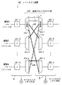
【課題を解決するための手段】
本発明では上記課題を解決するために、図1に示すような、入力光信号のWDM数がn、入力光信号の多重されている波長がλ1〜λmでWDM波長数がmの場合に、非閉塞の光クロスコネクトを行う光クロスコネクト装置10において、入力するλ1〜λmのm個の波長が多重されたWDM信号に対し、波長変換を行って、λ1〜λ2mの2m個の波長を生成するn個の第1の波長変換部11−1〜11−nと、第1の波長変換部11−1〜11−nによって波長変換された光信号を2m個の波長に分波するn個の第1の分波器12a−1〜12a−nと、分波後の2m個の波長の光信号を合波するn個の第1の合波器12b−1〜12b−nと、から構成され、第1の分波器12a−1〜12a−nと第1の合波器12b−1〜12b−nの接続を、2m/n本の接続束で波長が重複しないように接続して、波長単位のクロスコネクトを行う第1の波長クロスコネクト部12と、第1の波長クロスコネクト部12によってクロスコネクトされた後の2m個の波長が多重している光信号に対し、波長変換を行って、2m個の波長を生成するn個の第2の波長変換部13−1〜13−nと、第2の波長変換部13−1〜13−nによって波長変換された光信号を2m個の波長に分波するn個の第2の分波器14a−1〜14a−nと、分波後の2m個の波長の光信号を合波するn個の第2の合波器14b−1〜14b−nと、から構成され、第2の分波器14a−1〜14a−nと第2の合波器14b−1〜14b−nの接続を、2m/n本の接続束で波長が重複しないように接続して、波長単位のクロスコネクトを行う第2の波長クロスコネクト部14と、第2の波長クロスコネクト部14によってクロスコネクトされた後のλ1〜λ2mの2m個の波長が多重している光信号に対し、波長変換を行って、λ1〜λmのm個の波長を生成して送出するn個の第3の波長変換部15−1〜15−nと、を有することを特徴とする光クロスコネクト装置10が提供される。
【0011】
ここで、第1の波長変換部11−1〜11−nは、入力するλ1〜λmのm個の波長が多重されたWDM信号に対し、波長変換を行って、λ1〜λ2mの2m個の波長を生成する。第1の波長クロスコネクト部12は、第1の波長変換部11−1〜11−nによって波長変換された光信号を2m個の波長に分波するn個の第1の分波器12a−1〜12a−nと、分波後の2m個の波長の光信号を合波するn個の第1の合波器12b−1〜12b−nと、から構成され、第1の分波器12a−1〜12a−nと第1の合波器12b−1〜12b−nの接続を、2m/n本の接続束で波長が重複しないように接続して、波長単位のクロスコネクトを行う。第2の波長変換部13−1〜13−nは、第1の波長クロスコネクト部12によってクロスコネクトされた後の2m個の波長が多重している光信号に対し、波長変換を行って、2m個の波長を生成する。第2の波長クロスコネクト部14は、第2の波長変換部13−1〜13−nによって波長変換された光信号を2m個の波長に分波するn個の第2の分波器14a−1〜14a−nと、分波後の2m個の波長の光信号を合波するn個の第2の合波器14b−1〜14b−nと、から構成され、第2の分波器14a−1〜14a−nと第2の合波器14b−1〜14b−nの接続を、2m/n本の接続束で波長が重複しないように接続して、波長単位のクロスコネクトを行う。第3の波長変換部15−1〜15−nは、第2の波長クロスコネクト部14によってクロスコネクトされた後のλ1〜λ2mの2m個の波長が多重している光信号に対し、波長変換を行って、λ1〜λmのm個の波長を生成して送出する。
【0012】
【発明の実施の形態】
以下、本発明の実施の形態を図面を参照して説明する。図1は本発明の光クロスコネクト装置の原理図である。光クロスコネクト装置10は、入力光信号のWDM数がn(WDMルート数がn)、入力光信号の多重されている波長がλ1〜λmでWDM波長数(波長多重数)がmの場合に、非閉塞(非閉塞スイッチの内容については後述する)の光クロスコネクトを行う装置である。なお、図1に示す光クロスコネクト装置10を第1の実施の形態とする。
【0013】
光クロスコネクト装置10は、第1の波長変換部11−1〜11−n(以下、波長変換部11−1〜11−n)、第1の波長クロスコネクト部12(以下、波長クロスコネクト部12)、第2の波長変換部13−1〜13−n(以下、波長変換部13−1〜13−n)、第2の波長クロスコネクト部14(以下、波長クロスコネクト部14)、第3の波長変換部15−1〜15−n(以下、波長変換部15−1〜15−n)から構成される。なお、以降の説明で各構成要素を総称する場合は、ハイフン以下の数字は略す(例えば、波長変換部11−1〜11−nは、波長変換部11と記す)。
【0014】
波長変換部11−1〜11−nは、n個配置して、入力するλ1〜λmのm個の波長が多重されたWDM信号に対し、波長変換を行って、λ1〜λ2mの2m個の波長を生成する。
【0015】
波長クロスコネクト部12は、パッシブな光デバイスである、第1の分波器12a−1〜12a−n(以下、分波器12a−1〜12a−n)と第1の合波器12b−1〜12b−n(以下、合波器12b−1〜12b−n)とを含み、波長単位のクロスコネクトを行う。なお、本発明の分波器及び合波器には、AWG(Arrayed Waveguide Grating:アレイ導波路型光合分波器)を適用するものとする。
【0016】
分波器12a−1〜12a−nは、n個配置して、波長変換部11−1〜11−nによって波長変換された光信号を2m個の波長に分波する。合波器12b−1〜12b−nは、n個配置して、分波後の2m個の波長の光信号を合波する。また、分波器12a−1〜12a−nと合波器12b−1〜12b−nの接続は、2m/n本の接続束で各波長が重複しないように接続する(図中の太実線は2m/n本の束を表す)。
【0017】
波長変換部13−1〜13−nは、n個配置して、波長クロスコネクト部12によってクロスコネクトされた後の2m個の波長が多重している光信号に対し、波長変換を行って、2m個の波長を生成する。
【0018】
波長クロスコネクト部14は、第2の分波器14a−1〜14a−n(以下、分波器14a−1〜14a−n)と第2の合波器14b−1〜14b−n(以下、合波器14b−1〜14b−n)とを含み、波長単位のクロスコネクトを行う。
【0019】
分波器14a−1〜14a−nは、n個配置して、波長変換部13−1〜13−nによって波長変換された光信号を2m個の波長に分波する。合波器14b−1〜14b−nは、n個配置して、分波後の2m個の波長の光信号を合波する。また、分波器14a−1〜14a−nと合波器14b−1〜14b−nの接続は、2m/n本の接続束で各波長が重複しないように接続する。
【0020】
波長変換部15−1〜15−nは、波長クロスコネクト部14によってクロスコネクトされた後のλ1〜λ2mの2m個の波長が多重している光信号に対し、波長変換を行って、λ1〜λmのm個の波長を生成してWDM信号として送出する。
【0021】
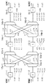
次にn=2、m=2の簡単な例を示して、光クロスコネクト装置(以降、本発明の光クロスコネクト装置をλベースXC装置とも呼ぶ)10の動作の流れについて説明する。図2はn=2、m=2のときのλベースXC装置の動作を説明するための図である。WDM1の入力光信号は、λα1、λα2の2つの波長が多重されており、WDM2の入力光信号は、λβ1、λβ2の2つの波長が多重されている。
【0022】
そしてここでは、光クロスコネクトを施した後、WDM1の装置出力側からはλα1、λβ2の波長が多重された光信号が送出し、WDM2の装置出力側からはλβ1、λα2の波長が多重された光信号が送出するものとする。
【0023】
波長変換部11−1は、λα1をλA、λBに変換し、λα2をλC、λDに変換して、波長数2を波長数4にする。波長変換部11−2は、λβ1をλa、λbに変換し、λα2をλc、λdに変換して、波長数2を波長数4にする(m→2m)。
【0024】
一方、合分波器間の接続は、2m/n本の接続束で各波長が重複しないように接続するのであるから、ここでは2本(=2・2/2)の接続束で、分波器12a−1からλA、λCの2本を合波器12b−1へつなぎ、分波器12a−1からλB、λDの2本を合波器12b−2へつなぐ。同様にして、分波器12a−2からλa、λcの2本を合波器12b−1へつなぎ、分波器12a−2からλb、λdの2本を合波器12b−2へつなぐ。そして、波長単位のクロスコネクトを行って、合波器12b−1、12b−2から合波信号が出力される。
【0025】
ここで、“波長が重複しないように接続する”とは、同じ波長が同一の合波器へ入力されないように接続するということである。すなわち、ここでは同じ接続束(2m/n本)の中に、同じ波長がだぶらないように接続する。例えば、分波器12a−1から合波器12b−1を接続する2本に対して、λA、λBとすると、これはλα1がだぶってしまうことになるので、上記のようにλA、λCを接続することになる。
【0026】
波長変換部13−1は、λA、λC、λa、λcが多重された信号を受信すると、λA→λE、λC→λF、λa→λG、λc→λHの変換を行い、波長変換部13−2は、λB、λD、λb、λdが多重された信号を受信すると、λB→λg、λD→λh、λb→λe、λd→λfの変換を行う。なお、波長変換後の波長数は、変換前の4波であり変わらない(2m→2m)。
【0027】
分波器14a−1からλE、λFの2本を合波器14b−1へつなぎ、分波器14a−1からλG、λHの2本を合波器14b−2へつなぐ。また、分波器14a−2からλe、λfの2本を合波器14b−1へつなぎ、分波器14a−2からλg、λhの2本を合波器14b−2へつなぐ。そして、波長単位のクロスコネクトを行って、合波器14b−1、14b−2から合波信号が出力される。
【0028】
波長変換部15−1は、λE、λF、λe、λfの合波信号を受信すると、λEとλfの波長変換を行ってλα1、λβ2を生成して、WDM1からλα1、λβ2の波長多重信号を送出する。また、波長変換部15−2は、λG、λH、λg、λhの合波信号を受信すると、λGとλhの波長変換を行ってλβ1、λα2を生成して、WDM2からλβ1、λα2の波長多重信号を送出する。
【0029】
次に波長変換部の構成について説明する。図3、図4は波長変換部の構成を示す図である。本発明の波長変換部は、分波器、波長変換素子、合波器から構成される(図1の波長変換部11、13、15を含め、以降で後述する実施の形態の波長変換部も同様な構成を持つ)。
【0030】
図3は、図2の波長変換部11−1について示している。波長変換部11−1は、分波器11a、波長変換素子11b−1〜11b−4、合波器11c、カプラC1、C2から構成される。分波器11aは、λα1、λα2が多重されている信号を波長毎に分波する。波長変換素子11b−1はλα1をλAに、波長変換素子11b−2はλα1をλBに変換する。
【0031】
また、波長変換素子11b−3はλα2をλCに、波長変換素子11b−4はλα2をλDに変換する。そして、合波器11cは、波長変換素子11b−1〜11b−4から出力されたλA、λB、λC、λDの信号を合波して出力する。
【0032】
図4は、図2の波長変換部15−1について示している。波長変換部15−1は、分波器15a、波長変換素子15b−1〜15b−4、合波器15c、カプラC3、C4から構成される。分波器15aは、λE、λF、λe、λfが多重されている信号を波長毎に分波する。波長変換素子15b−1はλEをλα1に、波長変換素子15b−2はλFをλα2に変換する。
【0033】
また、波長変換素子15b−3はλeをλβ1に、波長変換素子15b−4はλfをλβ2に変換する。なお、波長変換素子15b−1〜15b−4は、上位レイヤからの指示にもとづき動作する。そして、合波器15cは、カプラC3、C4を介して、ここでは波長変換素子15b−1、15b−4から出力されたλα1、λβ2の信号を合波して出力する。
【0034】
以上説明したように、λベースXC装置10においては、装置内で扱う波長数は、入力波長数mの2倍の2mとする。このことはすなわち、スイッチ通路を装置内では2倍用意しているということである(波長数=光路)。そして、時分割処理を行わずに2m個の波長をアロケートして、AWGのようなパッシブなデバイスを用いた合分波器によって光路を切り換えることにより、光クロスコネクトを実現している。
【0035】
これにより、MEMS等を用いて空間的に光路を切り換える従来技術と比較して、スイッチ素子の高度な製造性や複雑な制御性などに制限を受けることがないので、大規模のスイッチングを行うことができ、高スループットな光クロスコネクトを実現することが可能になる。
【0036】
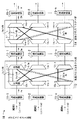
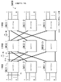
次にスイッチの閉塞、非閉塞について説明する。スイッチには、スイッチング時に目的ポートにパスを張ろうとすると、輻輳が生じるおそれのある閉塞(ブロッキング:blocking)タイプのスイッチと、スイッチング時に輻輳が生じることのない非閉塞(ノンブロッキング:non−blocking)タイプのスイッチとがあり、上記で説明したλベースXC装置10は輻輳が生じない完全非閉塞タイプのスイッチである。以下、閉塞タイプ、非閉塞タイプのスイッチの違いと、非閉塞タイプの空間スイッチの構成例について説明する。
【0037】
図5は閉塞タイプのスイッチの一例を示す図である。入線が2本、出線が2本の2×2のスイッチSW51〜SW54を、1段目にスイッチSW51、SW52を配置し、2段目にスイッチSW53、SW54を配置して、全体で4×4のスイッチを構成する。
【0038】
また、スイッチSW51は、入線側にポートp1a、p2a、出線側にポートp3a、p4aを有し、スイッチSW52は、入線側にポートp1b、p2b、出線側にポートp3b、p4bを有し、スイッチSW53は、入線側にポートp1c、p2c、出線側にポートp3c、p4cを有し、スイッチSW54は、入線側にポートp1d、p2d、出線側にポートp3d、p4dを有している。
【0039】
そして、ポートp3aとポートp1cがラインL1と接続し、ポートp4aとポートp1dがラインL2と接続し、ポートp3bとポートp2cがラインL3と接続し、ポートp4bとポートp2dがラインL4と接続する。
【0040】
このような構成に対し、図に示すパス(スイッチングパス)の向きについて記すと、パスP1(ポートp1a→ポートp3a)、パスP2(ポートp2a→ポートp4a)、パスP3(ポートp1b→ポートp3b)、パスP4(ポートp2b→ポートp4b)、パスP5(ポートp1c→ポートp3c)、パスP6(ポートp2c→ポートp4c)、パスP7(ポートp1d→ポートp3d)、パスP8(ポートp2d→ポートp4d)である。
【0041】
このようなパスによって、入信号(s1、s2、s3、s4)は、1段目のスイッチSW51、SW52の入線側から入力して、1段目及び2段目のスイッチによりスイッチングされると、2段目のスイッチSW53、SW54の出線側から出信号(s1、s3、s2、s4)の並びで出力されることになる。
【0042】
ここで、この状態から、信号s3と信号s2はそのままで、信号s1と信号s4の順番を入れ替えて、入信号(s1、s2、s3、s4)を出信号(s4、s3、s2、s1)の並びにスイッチングする場合を考える。
【0043】
信号s1の経路について見ると、スイッチSW51のパスP1は、ポートp1a→ポートp4aへ向け、ラインL2を通った後に、スイッチSW54のパスP7の向きをポートp1d→ポートp4dへ向けることになる。また、信号s4の経路について見ると、スイッチSW52のパスP4は、ポートp2b→ポートp3bへ向け、ラインL3を通った後に、スイッチSW53のパスP6の向きをポートp2c→ポートp3cへ向けることになる。
【0044】
ところが、このようなスイッチング操作を行ってしまうと、それぞれのスイッチ内のパスが輻輳してしまうことがわかる(例えば、スイッチSW51では、パスP1とパスP2がポート4aでぶつかってしまう)。このため、上記の場合、信号s1、s4のみの順番を入れ替えることはできず、信号s1、s4の順番を入れ替えるためには、信号s2、s3の順番まで入れ替えなければならないことになる(結局、出信号(s4、s2、s3、s1)とするしかない)。
【0045】
ここで、m×mの閉塞スイッチでは、入線m−1本に対応する出線が確立してしまうと、スイッチ内の残りの1本のパスの行き先が決まってしまう。例えば、図5のスイッチSW51では、ラインL2を通すパスP2が確立してしまうと、もう一方のパスP1はラインL1に向かうしかない(最も本数の少ない例である)。このような構成の閉塞タイプのスイッチでは、ある箇所のスイッチングを行おうとすると、上述のように他の箇所まで影響を与えてしまうことになる。
【0046】
図6は非閉塞タイプのスイッチの一例を示す図である。入線が2本、出線が4本の2×4のスイッチSW61〜SW64を、1段目にスイッチSW61、SW62を配置し、2段目にスイッチSW63、SW64を配置して、全体で4×4のスイッチを構成する。
【0047】
また、スイッチSW61は、入線側にポートp1a、p2a、出線側にポートp3a〜p6aを有し、スイッチSW62は、入線側にポートp1b、p2b、出線側にポートp3b〜p6bを有し、スイッチSW63は、入線側にポートp1c〜p4c、出線側にポートp5c、p6cを有し、スイッチSW64は、入線側にポートp1d〜p4d、出線側にポートp5d、p6dを有している。
【0048】
そして、ポートp3aとポートp1cがラインL1と接続し、ポートp4aとポートp2cがラインL2と接続し、ポートp5aとポートp1dがラインL3と接続し、ポートp6aとポートp2dがラインL4と接続する。
【0049】
さらに、ポートp3bとポートp3cがラインL5と接続し、ポートp4bとポートp4cがラインL6と接続し、ポートp5bとポートp3dがラインL7と接続し、ポートp6bとポートp4dがラインL8と接続する。
【0050】
このような構成に対し、図に示すパス(スイッチングパス)の向きについて記すと、パスP1(ポートp1a→ポートp3a)、パスP2(ポートp2a→ポートp6a)、パスP3(ポートp1b→ポートp3b)、パスP4(ポートp2b→ポートp6b)、パスP5(ポートp1c→ポートp5c)、パスP7(ポートp3c→ポートp6c)、パスP10(ポートp2d→ポートp5d)、パスP12(ポートp4d→ポートp6d)である。
【0051】
このようなパスによって、入信号(s1、s2、s3、s4)は、1段目のスイッチSW61、SW62の入線側から入力して、1段目及び2段目のスイッチによりスイッチングされると、2段目のスイッチSW63、SW64の出線側から出信号(s1、s3、s2、s4)の並びで出力されることになる。
【0052】
ここで、この状態から、信号s3と信号s2はそのままで、信号s1と信号s4の順番を入れ替えて、入信号(s1、s2、s3、s4)を出信号(s4、s3、s2、s1)の並びにスイッチングする場合を考える。
【0053】
図7はスイッチング後のパス状態を示す図である。信号s1の経路について見ると、スイッチSW61のパスP1は、ポートp1a→ポートp5aへ向け、ラインL3を通った後に、スイッチSW64からパスP9の向きをポートp1dからポートp6dへ向けることになる。また、信号s4の経路について見ると、スイッチSW62のパスP4は、ポートp2b→ポートp4bへ向け、ラインL6を通った後に、スイッチSW63からパスP8の向きをポートp4cからポートp5cへ向けることになる。
【0054】
図からわかるように、このようなスイッチング操作を行っても、それぞれのスイッチ内のパスが輻輳することはない(信号s3、s2の経路はそのまま)。したがって、信号s1、s4のみの順番を入れ替えることができ、信号(s4、s3、s2、s1)とすることができる。
【0055】
このように、入線の本数に対して、およそ2倍近くの本数の出線を持つスイッチを多段に組み合わせれば、入線m−1本に対応する出線が確立しても、スイッチ内の残り1本のパスの行き先が固定的に決まってしまうことはなくなる。例えば、図7のスイッチSW61では、ラインL4を通すパスP2が確立しても、もう一方のパスP1は残り3通り(ポートp3a〜p5a)のラインL1〜L3の選択性がある。このような構成の非閉塞タイプのスイッチでは、他の箇所に影響を与えることなく、ある箇所のスイッチングを自由に行うことができる。
【0056】
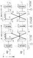
次に非閉塞タイプの空間スイッチの例について図8〜図11を用いて説明する。図8は非閉塞タイプの空間スイッチの構成を示す図である。空間スイッチSW10は、2段構成からなり、1段目に入線がm本、出線がm・n本のm×m・nのスイッチSW11−1〜SW11−nと、2段目に入線がm・n本、出線がm本のm・n×mのスイッチSW12−1〜SW12−nとから構成され、全体でm・n×m・nのスイッチである。また、1段目のm×m・nスイッチはn個、2段目のm・n×mスイッチはn個なので、全体でm×m・nスイッチが2n個ある(1段目と2段目は同じスイッチ)。
【0057】
さらに、1段目のスイッチSW11−1の出線は、m本のラインの束がnあり、m本の各ライン束は、2段目のスイッチSW12−1〜SW12−nとそれぞれ接続する。スイッチSW11−2〜SW11−nからの出線も同様にして、2段目のスイッチSW12−1〜SW12−nとそれぞれ接続する。
【0058】
ここで、1段目の単位スイッチ(スイッチSW11−1〜SW11−nのいずれかのスイッチのこと)の入線m−1本に対応する出線が確立した場合、残り1本が張れるパスの本数は、出線本数から(m−1)を引いて、m・n−(m−1)=m(n−1)+1である。したがって、m(n−1)+1通りに自由にパスが張れるので、空間スイッチSW10は非閉塞タイプである。
【0059】
図9は非閉塞タイプの空間スイッチの構成を示す図である。空間スイッチSW20は、3段構成からなり、1段目に入線がm本、出線が(2m−1)本のm×(2m−1)のスイッチSW21−1〜SW21−nと、2段目に入線がn本、出線がn本のn×nのスイッチSW22−1〜SW22−(2m−1)と、3段目に入線が(2m−1)本、出線がm本の(2m−1)×mのスイッチSW23−1〜SW23−nとから構成され、全体でm・n×m・nのスイッチである。
【0060】
また、1段目のm×(2m−1)スイッチがn個、2段目のn×nスイッチが(2m−1)個、3段目の(2m−1)×mスイッチがn個なので、全体でm×(2m−1)スイッチが2n個(1段目と3段目は同じスイッチ)、n×nスイッチが(2m−1)個ある。
【0061】
さらに、1段目のスイッチSW21−1の出線は、2m−1本なので、1本づつ2段目のスイッチSW22−1〜SW22−(2m−1)とそれぞれ接続する。スイッチSW21−2〜SW21−nからの出線も同様にして、2段目のスイッチSW22−1〜SW22−(2m−1)とそれぞれ接続する。
【0062】
また、2段目のスイッチSW22−1の出線は、n本なので、1本づつ3段目のスイッチSW23−1〜SW23−nとそれぞれ接続する。スイッチSW22−2〜SW22−(2m−1)からの出線も同様にして、3段目のスイッチSW23−1〜SW23−nとそれぞれ接続する。
【0063】
ここで、1段目の単位スイッチの出線は(2m−1)本であるから、1段目の単位スイッチから2段目の(2m−1)個のスイッチSW22−1〜22−(2m−1)へ向かうパスの本数は(2m−1)本である。また、3段目の単位スイッチの入線は(2m−1)本であるから、2段目の(2m−1)個のスイッチSW22−1〜22−(2m−1)それぞれから3段目の単位スイッチへ向かうパスの本数は(2m−1)本である。
【0064】
したがって、1段目スイッチの入線m−1本に対応する出線が確立し、3段目スイッチの入線m−1本に対応する出線が確立した場合でも、(2m−1)−(m−1)=m本のパスが1段目→3段目に張ることができるので、空間スイッチSW20は非閉塞タイプである。なお、多段構成の非閉塞スイッチは、Clos型スイッチとも呼ばれる(Charles Closによって提案されたことによる)。
【0065】
図10は非閉塞タイプの空間スイッチの構成を示す図である。図9の変形例である空間スイッチSW30は、3段構成からなり、1段目に入線がm本、出線が2m本のm×2mのスイッチSW31−1〜SW31−nと、2段目に入線がm本、出線がm本のm×mのスイッチSW32−1〜SW32−2nと、3段目に入線が2m本、出線がm本の2m×mのスイッチSW33−1〜SW33−nとから構成され、全体でm・n×m・nのスイッチである(m>nでm、nは偶数)。
【0066】
また、1段目のm×2mスイッチがn個、2段目のm×mスイッチが2n個、3段目の2m×mスイッチがn個なので、全体でm×2mスイッチが2n個(1段目と3段目は同じスイッチ)、m×mスイッチが2n個ある。
【0067】
さらに、1段目のスイッチSW31−1の出線は2m本であり、この2m本がm/n(m/nは整数)本のライン束ごとに2段目のスイッチSW32−1〜SW32−2nとそれぞれ接続する。スイッチSW31−2〜SW32−nからの出線も同様にして、2段目のスイッチSW32−1〜SW32−2nとそれぞれ接続する。
【0068】
また、2段目のスイッチSW32−1の出線はm本であり、このm本がm/n本のライン束ごとに3段目のスイッチSW33−1〜SW33−nとそれぞれ接続する。スイッチSW32−2〜SW32−nからの出線も同様にして、3段目のスイッチSW33−1〜SW33−nとそれぞれ接続する。
【0069】
ここで、1段目の単位スイッチの出線は2m本であるから、1段目の単位スイッチから2段目の2n個のスイッチSW32−1〜32−2nへ向かうパスの本数は2m本である。また、3段目の単位スイッチの入線は2m本であるから、2段目の2n個のスイッチSW32−1〜32−2nそれぞれから3段目の単位スイッチへ向かうパスの本数は2m本である。
【0070】
したがって、1段目スイッチの入線m−1本に対応する出線が確立し、3段目スイッチの入線m−1本に対応する出線が確立した場合でも、2m−(m−1)=(m+1)本のパスが1段目→3段目に張ることができるので、空間スイッチSW30は非閉塞タイプである。
【0071】
図11は非閉塞タイプの空間スイッチの構成を示す図である。図9の変形例である空間スイッチSW40は、3段構成からなり、1段目に入線がm本、出線が2m本のm×2mのスイッチSW41−1〜SW41−nと、2段目に入線が2m本、出線が2m本の2m×2mのスイッチSW42−1〜SW42−nと、3段目に入線が2m本、出線がm本の2m×mのスイッチSW43−1〜SW43−nとから構成され、全体でm・n×m・nのスイッチである(m、nは偶数)。
【0072】
また、1段目のm×2mスイッチがn個、2段目の2m×2mスイッチがn個、3段目の2m×mスイッチがn個なので、全体でm×2mスイッチが2n個(1段目と3段目は同じスイッチ)、2m×2mスイッチがn個ある(図10で示した空間スイッチSW30よりもスイッチ構成数は少なくなる)。
【0073】
さらに、1段目のスイッチSW41−1の出線は2m本であり、この2m本が2m/n(2m/nは整数)本のライン束ごとに2段目のスイッチSW42−1〜SW42−nとそれぞれ接続する。スイッチSW41−2〜SW41−nからの出線も同様にして、2段目のスイッチSW42−1〜SW42−nとそれぞれ接続する。
【0074】
また、2段目のスイッチSW42−1の出線は2m本であり、この2m本が2m/n本のライン束ごとに3段目のスイッチSW43−1〜SW43−nとそれぞれ接続する。スイッチSW42−2〜SW42−nからの出線も同様にして、3段目のスイッチSW43−1〜SW43−nとそれぞれ接続する。
【0075】
ここで、1段目の単位スイッチの出線は2m本であるから、1段目の単位スイッチから2段目のn個のスイッチSW42−1〜42−nへ向かうパスの本数は2m本である。また、3段目の単位スイッチの入線は2m本であるから、2段目のn個のスイッチSW42−1〜42−2nそれぞれから3段目の単位スイッチへ向かうパスの本数は2m本である。
【0076】
したがって、1段目スイッチの入線m−1本に対応する出線が確立し、3段目スイッチの入線m−1本に対応する出線が確立した場合でも、2m−(m−1)=(m+1)本のパスが1段目→3段目に張ることができるので、空間スイッチSW40は非閉塞タイプである。
【0077】
次にλベースXC装置10と、図11に示した空間スイッチSW40との対応関係について説明する。図12、図13はλベースXC装置10と空間スイッチSW40との対応関係を示す図である。λベースXC装置10の波長変換部11の入力から波長クロスコネクト部12内の分波器12aの出力までの区間Aは、空間スイッチSW40の1段目のm×2mスイッチに対応する。
【0078】
また、波長クロスコネクト部12内の合波器12bの入力から波長クロスコネクト部14内の分波器14aの出力までの区間Bは、空間スイッチSW40の2段目の2m×2mスイッチに対応する。さらに、波長クロスコネクト部14内の合波器14bの入力から波長変換部15の出力までの区間Cは、空間スイッチSW40の3段目の2m×mスイッチに対応する。
【0079】
一方、空間スイッチSW40の区間aに対し、λベースXC装置10の波長変換部11に対するWDM1〜WDMnの物理的な入力線は1本であるが、波長がλ1〜λmであるため、波長レベルでみると、m本の信号入力としてよく、m×2mスイッチの入線数と等しい。
【0080】
区間bに対し、n個の分波器12aの出力ファイバは2m/n本束ねて、n個の合波器12bそれぞれに接続するので、m×2mスイッチの出線と2m×2mスイッチの入線との関係と等しい。
【0081】
区間cに対し、n個の分波器14aの出力ファイバは2m/n本束ねて、n個の合波器14bそれぞれに接続するので、2m×2mスイッチの出線と2m×mスイッチの入線との関係と等しい。
【0082】
区間dに対し、λベースXC装置10に対する波長変換部15のWDM1〜WDMnの物理的な出力線は1本であるが、波長がλ1〜λmであるため、波長レベルでみると、m本の信号出力としてよく、2m×mスイッチの出線数と等しい。したがって、λベースXC装置10は、空間スイッチSW40と等価的に等しい構成を持つので、非閉塞スイッチとなる。
【0083】
なお、本発明のλベースXC装置は、空間スイッチは使用せずに、空間スイッチの非閉塞タイプとなるスイッチング理論を適用して、波長ベースで光路を切り換えるものである。
【0084】
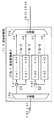
次に第2の実施の形態のλベースXC装置について説明する。図14は第2の実施の形態のλベースXC装置の構成を示す図である。λベースXC装置20は、図10に示した非閉塞の空間スイッチSW30を応用した装置である。
【0085】
波長変換部21−1〜21−nは、n個配置して、入力するλ1〜λmのm個の波長が多重されたWDM信号に対し、波長変換を行って、λ1〜λ2mの2m個の波長を生成する。
【0086】
波長クロスコネクト部22は、分波器22a−1〜22a−nと合波器22b−1〜22b−2nとを含み、波長単位のクロスコネクトを行う。分波器22a−1〜22a−nは、n個配置して、波長変換部21−1〜21−nによって波長変換された光信号を2m個の波長に分波する。合波器22b−1〜22b−2nは、2n個配置して、分波後のm個の波長の光信号を合波する。また、分波器22a−1〜22a−nと合波器22b−1〜22b−2nの接続は、m/n本の接続束で波長が重複しないように接続する(図中の太実線はm/n本の束を表す)。
【0087】
波長変換部23−1〜23−2nは、2n個配置して、波長クロスコネクト部22によってクロスコネクトされた後のm個の波長が多重している光信号に対し、波長変換を行って、m個の波長を生成する。
【0088】
波長クロスコネクト部24は、分波器24a−1〜24a−2nと合波器24b−1〜24b−nとを含み、波長単位のクロスコネクトを行う。分波器24a−1〜24a−2nは、2n個配置して、波長変換部23−1〜23−2nによって波長変換された光信号をm個の波長に分波する。合波器24b−1〜24b−nはn個配置して、分波後の2m個の波長数の光信号を合波する。また、分波器24a−1〜24a−2nと合波器24b−1〜24b−nの接続は、m/n本の接続束で波長が重複しないように接続する。
【0089】
波長変換部25−1〜25−nは、n個配置して、波長クロスコネクト部24によってクロスコネクトされた後のλ1〜λ2mの2m個の波長が多重している光信号に対し、波長変換を行って、λ1〜λmのm個の波長を生成して送出する。
【0090】
次にλベースXC装置20と空間スイッチSW30との対応関係について説明する。図15、図16はλベースXC装置20と空間スイッチSW30との対応関係を示す図である。λベースXC装置20の波長変換部21の入力から波長クロスコネクト部22内の分波器22aの出力までの区間Aは、空間スイッチSW30の1段目のm×2mスイッチに対応する。
【0091】
また、波長クロスコネクト部22内の合波器22bの入力から波長クロスコネクト部24内の分波器24aの出力までの区間Bは、空間スイッチSW30の2段目のm×mスイッチに対応する。さらに、波長クロスコネクト部24内の合波器24bの入力から波長変換部25の出力までの区間Cは、空間スイッチSW30の3段目の2m×mスイッチに対応する。
【0092】
一方、空間スイッチSW30の区間aに対し、λベースXC装置20の波長変換部21に対するWDM1〜WDMnの物理的な入力線は1本であるが、波長がλ1〜λmであるため、波長レベルでみると、m本の信号入力としてよく、m×2mスイッチの入線数と等しい。
【0093】
区間bに対し、n個の分波器22aの出力ファイバはm/n本束ねて、2n個の合波器22bそれぞれに接続するので、m×2mスイッチの出線とm×mスイッチの入線との関係と等しい。
【0094】
区間cに対し、2n個の分波器24aの出力ファイバはm/n本束ねて、n個の合波器24bそれぞれに接続するので、m×mスイッチの出線と2m×mスイッチの入線との関係と等しい。
【0095】
区間dに対し、λベースXC装置20に対する波長変換部25のWDM1〜WDMnの物理的な出力線は1本であるが、波長がλ1〜λmであるため、波長レベルでみると、m本の信号出力としてよく、2m×mスイッチの出線数と等しい。したがって、λベースXC装置20は、空間スイッチSW30と等価的に等しい構成を持つので、非閉塞スイッチとなる。
【0096】
次に第3の実施の形態のλベースXC装置について説明する。図17は第3の実施の形態のλベースXC装置の構成を示す図である。λベースXC装置30は、図9に示した非閉塞の空間スイッチSW20を応用した装置である。
【0097】
波長変換部31−1〜31−nは、n個配置して、入力するλ1〜λmのm個の波長が多重されたWDM信号に対し、波長変換を行って、λ1〜λ2m−1の2m−1個の波長を生成する。
【0098】
波長クロスコネクト部32は、分波器32a−1〜32a−nと合波器32b−1〜32b−(2m−1)とを含み、波長単位のクロスコネクトを行う。分波器32a−1〜32a−nは、n個配置して、波長変換部31−1〜31−nによって波長変換された光信号を2m−1個の波長に分波する。合波器32b−1〜32b−(2m−1)は、2m−1個配置して、分波後のn個の波長の光信号を合波する。また、分波器32a−1〜32a−nと合波器32b−1〜32b−(2m−1)の接続はそれぞれ1本で接続する。
【0099】
波長変換部33−1〜33−(2m−1)は、2m−1個配置して、波長クロスコネクト部32によってクロスコネクトされた後のn個の波長が多重している光信号に対し、波長変換を行って、n個の波長を生成する。
【0100】
波長クロスコネクト部34は、分波器34a−1〜34a−(2m−1)と合波器34b−1〜34b−nとを含み、波長単位のクロスコネクトを行う。分波器34a−1〜34a−(2m−1)は、2m−1個配置して、波長変換部33−1〜33−(2m−1)によって波長変換された光信号をn個の波長に分波する。合波器34b−1〜34b−nは、n個配置して、分波後の2m−1個の波長の光信号を合波する。また、分波器34a−1〜34a−(2m−1)と合波器34b−1〜34b−nの接続はそれぞれ1本で接続する。
【0101】
波長変換部35−1〜35−nは、波長クロスコネクト部34によってクロスコネクトされた後のλ1〜λ2m−1の2m−1個の波長が多重している光信号に対し、波長変換を行って、λ1〜λmのm個の波長を生成して送出する。
【0102】
次にλベースXC装置30と空間スイッチSW20との対応関係について説明する。図18、図19はλベースXC装置30と空間スイッチSW20との対応関係を示す図である。λベースXC装置30の波長変換部31の入力から波長クロスコネクト部32内の分波器32aの出力までの区間Aは、空間スイッチSW20の1段目のm×(2m−1)スイッチに対応する。
【0103】
また、波長クロスコネクト部32内の合波器22bの入力から波長クロスコネクト部34内の分波器34aの出力までの区間Bは、空間スイッチSW20の2段目のn×nスイッチに対応する。さらに、波長クロスコネクト部34内の合波器34bの入力から波長変換部35の出力までの区間Cは、空間スイッチSW20の3段目の(2m−1)×mスイッチに対応する。
【0104】
一方、空間スイッチSW20の区間aに対し、λベースXC装置30の波長変換部31に対するWDM1〜WDMnの物理的な入力線は1本であるが、波長がλ1〜λmであるため、波長レベルでみると、m本の信号入力としてよく、m×(2m−1)スイッチの入線数と等しい。
【0105】
区間bに対し、n個の分波器32aの出力ファイバは1本で、2m−1個の合波器32bそれぞれに接続するので、m×(2m−1)スイッチの出線とn×nスイッチの入線との関係と等しい。
【0106】
区間cに対し、2m−1個の分波器34aの出力ファイバは1本で、n個の合波器34bそれぞれに接続するので、n×nスイッチの出線と(2m−1)×mスイッチの入線との関係と等しい。
【0107】
区間dに対し、λベースXC装置30に対する波長変換部35のWDM1〜WDMnの物理的な出力線は1本であるが、波長がλ1〜λmであるため、波長レベルでみると、m本の信号出力としてよく、(2m−1)×mスイッチの出線数と等しい。したがって、λベースXC装置30は、空間スイッチSW20と等価的に等しい構成を持つので、非閉塞スイッチとなる。
【0108】
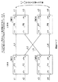
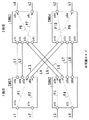
次に第4の実施の形態のλベースXC装置について説明する。図20は第4の実施の形態のλベースXC装置の構成を示す図である。λベースXC装置40は、図8に示した非閉塞の空間スイッチSW10を応用した装置である。
【0109】
入力側波長変換部41−1〜41−n(以下、波長変換部41−1〜41−n)は、n個配置して、入力するλ1〜λmのm個の波長が多重されたWDM信号に対し、波長変換を行って、λ1〜λmnのm・n個の波長を生成する。
【0110】
波長クロスコネクト部42は、分波器42a−1〜42a−nと、合波器42b−1〜42b−nとを含み、波長単位のクロスコネクトを行う。分波器42a−1〜42a−nは、n個配置して、波長変換部41−1〜41−nによって波長変換された光信号をm・n個の波長に分波する。合波器42b−1〜42b−nは、n個配置して、分波後のm・n個の波長の光信号を合波する。また、分波器42a−1〜42a−nと合波器42b−1〜42b−nの接続は、m本の接続束で波長が重複しないように接続する。
【0111】
出力側波長変換部43−1〜43−nは、n個配置して、波長クロスコネクト部42によってクロスコネクトされた後のλ1〜λmnのm・n個の波長が多重している光信号に対し、波長変換を行って、λ1〜λmのm個の波長を生成して送出する。
【0112】
次にλベースXC装置40と空間スイッチSW10との対応関係について説明する。図21、図22はλベースXC装置40と空間スイッチSW10との対応関係を示す図である。λベースXC装置40の波長変換部41の入力から波長クロスコネクト部42内の分波器42aの出力までの区間Aは、空間スイッチSW10の1段目のm×mnスイッチに対応する。
【0113】
また、波長クロスコネクト部42内の合波器42bの入力から波長変換部43の出力までの区間Bは、空間スイッチSW10の2段目のmn×nスイッチに対応する。
【0114】
一方、空間スイッチSW10の区間aに対し、λベースXC装置40の波長変換部41に対するWDM1〜WDMnの物理的な入力線は1本であるが、波長がλ1〜λmであるため、波長レベルでみると、m本の信号入力としてよく、m×mnスイッチの入線数と等しい。
【0115】
区間bに対し、n個の分波器42aの出力ファイバはm本束ねて、n個の合波器42bそれぞれに接続するので、m×mnスイッチの出線とmn×mスイッチの入線との関係と等しい。
【0116】
区間cに対し、λベースXC装置40に対する波長変換部43のWDM1〜WDMnの物理的な出力線は1本であるが、波長がλ1〜λmであるため、波長レベルでみると、m本の信号出力としてよく、mn×mスイッチの出線数と等しい。したがって、λベースXC装置40は、空間スイッチSW10と等価的に等しい構成を持つので、非閉塞スイッチとなる。
【0117】
次に第5の実施の形態のλベースXC装置について説明する。図23は第5の実施の形態のλベースXC装置の構成を示す図である。上記で説明した第1の実施の形態〜第4の実施の形態のλベースXC装置は、すべて完全非閉塞タイプの光クロスコネクトを行う装置であるが、第5の実施の形態のλベースXC装置50は、閉塞タイプの光クロスコネクトを行う装置である。λベースXC装置50は、閉塞タイプなので輻輳のおそれがあるが、従来技術と比べると大規模スイッチング及び高スループットが可能なので、ある程度、運用対象が限定できる場合に適用することについては有効である。
【0118】
波長変換部(入力側波長変換部)51−1〜51−nは、n個配置して、入力するλ1〜λmのm個の波長が多重されたWDM信号に対し、波長変換を行って、m個の波長を生成する。
【0119】
波長クロスコネクト部52は、m個の波長を分波するn個の分波器52a−1〜52a−nと、m個の波長を合波するn個の合波器52b−1〜52b−nとを含み、波長単位のクロスコネクトを行う。
【0120】
波長変換部(出力側波長変換部)53−1〜53−nは、n個配置して、波長クロスコネクト部52によってクロスコネクトされた後の光信号に対し、波長変換を行って、λ1〜λmのm個の波長を生成して送出する。
【0121】
次に第1の実施の形態〜第5の実施の形態のλベースXC装置に関する装置規模について説明する。図24、図25はλベースXC装置の装置規模を示す図である。テーブルT1は、λベースXC装置10〜50に対する、波長クロスコネクト部で使用する合分波器(AWGとする)と、波長変換部で使用するAWGとを示しており、テーブルT2は、波長変換部の数を示している。
【0122】
なお、以降では、M本の分波出力線を持つAWG(分波器)、またはM本の合波入力線を持つAWG(合波器)のことをMλのAWGと呼ぶ。例えば、波長多重数mの光信号をm本の分波出力線から波長毎に分波するAWGは、mλのAWGである。また、m個の波長の各信号をm本の合波入力線を通じて合波するAWGは、mλのAWGである。
【0123】
λベースXC装置10(図1)の装置規模を見ると、波長クロスコネクト部12内のAWGの個数は、2mλのAWG12a−1〜12a−nがn個、2mλのAWG12b−1〜12b−nがn個である。波長クロスコネクト部14内のAWGの個数は、2mλのAWG14a−1〜14a−nがn個、2mλのAWG14b−1〜14b−nがn個である。したがって、波長クロスコネクト部内の2mλのAWGは全部で4n個ある。
【0124】
また、波長変換部11−1〜11−nに含まれるAWGの個数は、分波器側のmλのAWGがn個、合波器側の2mλのAWGがn個である。波長変換部15−1〜15−nに含まれるAWGの個数は、分波器側の2mλのAWGがn個、合波器側のmλのAWGがn個である。
【0125】
さらに、波長変換部13−1〜13−nに含まれるAWGの個数は、分波器側の2mλのAWGがn個、合波器側の2mλのAWGがn個である。したがって、波長変換部全体のmλのAWGは2n個、2mλのAWGは4n個ある。
【0126】
なお、波長変換部の数で見ると、波長多重数mと波長多重数2mの変換を行う波長変換部は、波長変換部11−1〜11−nと波長変換部15−1〜15−nなので2n個である。また、波長多重数2mと波長多重数2mの変換を行う波長変換部は、波長変換部13−1〜13−nなのでn個である。
【0127】
λベースXC装置20(図14)の装置規模を見ると、波長クロスコネクト部22内のAWGの個数は、2mλのAWG22a−1〜22a−nがn個、mλのAWG22b−1〜22b−2nが2n個である。波長クロスコネクト部24内のAWGの個数は、mλのAWG24a−1〜24a−2nが2n個、2mλのAWG24b−1〜24b−nがn個である。したがって、波長クロスコネクト部内の2mλのAWGは2n個、mλのAWGは4n個ある。
【0128】
また、波長変換部21−1〜21−nに含まれるAWGの個数は、分波器側のmλのAWGがn個、合波器側の2mλのAWGがn個である。波長変換部25−1〜25−nに含まれるAWGの個数は、分波器側の2mλのAWGがn個、合波器側のmλのAWGがn個である。さらに、波長変換部23−1〜23−2nに含まれるAWGの個数は、分波器側のmλのAWGが2n個、合波器側のmλのAWGが2n個である。したがって、波長変換部全体のmλのAWGは6n個、2mλのAWGは2n個ある。
【0129】
なお、波長変換部の数で見ると、波長多重数mと波長多重数2mの変換を行う波長変換部は、波長変換部21−1〜21−nと波長変換部25−1〜25−nなので2n個である。また、波長多重数mと波長多重数mの変換を行う波長変換部は、波長変換部23−1〜23−2nなので2n個である。λベースXC装置20(図14)は、λベースXC装置10(図1)に比べて、2mλの大規模なAWGの個数を削減することができる。
【0130】
λベースXC装置30(図17)の装置規模を見ると、波長クロスコネクト部32内のAWGの個数は、(2m−1)λのAWG32a−1〜32a−nがn個、nλのAWG32b−1〜32b−(2m−1)が2m−1個である。波長クロスコネクト部34内のAWGの個数は、nλのAWG34a−1〜34a−(2m−1)が2m−1個、(2m−1)λのAWG34b−1〜34b−nがn個である。したがって、波長クロスコネクト部内の(2m−1)λのAWGは2n個、nλのAWGは2・(2m−1)個ある。
【0131】
また、波長変換部31−1〜31−nに含まれるAWGの個数は、分波器側のmλのAWGがn個、合波器側の(2m−1)λのAWGがn個である。波長変換部35−1〜35−nに含まれるAWGの個数は、分波器側の(2m−1)λのAWGがn個、合波器側のmλのAWGがn個である。さらに、波長変換部33−1〜33−(2m−1)に含まれるAWGの個数は、分波器側のnλのAWGが(2m−1)個、合波器側のnλのAWGが(2m−1)個である。したがって、波長変換部全体のmλのAWGは2n個、(2m−1)λのAWGは2n個、nλのAWGは2・(2m−1)個ある。
【0132】
なお、波長変換部の数で見ると、波長多重数mと波長多重数2m−1の変換を行う波長変換部は、波長変換部31−1〜31−nと波長変換部35−1〜35−nなので2n個である。また、波長多重数nと波長多重数nの変換を行う波長変換部は、波長変換部33−1〜33−(2m−1)なので(2m−1)個である。
【0133】
λベースXC装置30(図17)は、λベースXC装置10(図1)やλベースXC装置20(図14)と比べると、2mλのAWGを使用しないので、大規模なAWGの使用個数は少なくなるが、素子数は多くなる。
【0134】
λベースXC装置40(図20)の装置規模を見ると、波長クロスコネクト部42内のAWGの個数は、mnλのAWG42a−1〜42a−nがn個、mnλのAWG42b−1〜42b−nがn個である。したがって、波長クロスコネクト部内のmnλのAWGは2n個ある。
【0135】
また、波長変換部41−1〜41−nに含まれるAWGの個数は、分波器側のmλのAWGがn個、合波器側のmnλのAWGがn個である。波長変換部43−1〜43−nに含まれるAWGの個数は、分波器側のmnλのAWGがn個、合波器側のmλのAWGがn個である。したがって、波長変換部全体のmλのAWGは2n個、mnλのAWGは2n個ある。
【0136】
なお、波長変換部の数で見ると、波長多重数mと波長多重数mnの変換を行う波長変換部は、波長変換部41−1〜41−nと波長変換部43−1〜43−nなので2n個である。λベースXC装置40(図20)は、mnλの大規模なAWGが可能であるならば、最もシンプルな構成となる。
【0137】
λベースXC装置50(図23)の装置規模を見ると、波長クロスコネクト部52内のAWGの個数は、mλのAWG52a−1〜52a−nがn個、mλのAWG52b−1〜52b−nがn個である。したがって、波長クロスコネクト部内のmλのAWGは2n個ある。
【0138】
また、波長変換部51−1〜51−nに含まれるAWGの個数は、分波器側のmλのAWGがn個、合波器側のmλのAWGがn個である。波長変換部53−1〜53−nに含まれるAWGの個数は、分波器側のmλのAWGがn個、合波器側のmλのAWGがn個である。したがって、波長変換部内のmλのAWGは4n個ある。
【0139】
なお、波長変換部の数で見ると、波長多重数mと波長多重数mの変換を行う波長変換部は、波長変換部51−1〜51−nと波長変換部53−1〜53−nなので2n個である。λベースXC装置50(図23)は、閉塞タイプなので、適用環境または仕様を選択する必要がある。
【0140】
以上説明したように、本発明のλベースXC装置は、波長ベースで光路を切り換える構成としたので、従来のOXCのように空間スイッチが不要となり、大規模のスイッチングを行って高スループットな光クロスコネクトを実現することが可能になる。なお、合波器、分波器の規模とコスト等の状況から、本発明の実施の形態の中から最適な装置構成を選択することができる。
【0141】
【発明の効果】
以上説明したように、本発明の光クロスコネクト装置は、入力光信号のWDM数がn、WDM波長数がmの場合に、第1〜第3の波長変換部では、λ1〜λ2mまでの波長変換を行い、第1、第2の波長クロスコネクト部では、λ1〜λ2mまでの波長を扱う分波器と合波器とで構成し、分波器と合波器の接続は、2m/n本の接続束により各波長が重複しないように接続して、波長単位に光クロスコネクトを行う構成とした。これにより、大規模のスイッチングを行って高スループットな光クロスコネクトを実現することが可能になる。
【図面の簡単な説明】
【図1】本発明の光クロスコネクト装置の原理図である。
【図2】n=2、m=2のときのλベースXC装置の動作を説明するための図である。
【図3】波長変換部の構成を示す図である。
【図4】波長変換部の構成を示す図である。
【図5】閉塞タイプのスイッチの一例を示す図である。
【図6】非閉塞タイプのスイッチの一例を示す図である。
【図7】スイッチング後のパス状態を示す図である。
【図8】非閉塞タイプの空間スイッチの構成を示す図である。
【図9】非閉塞タイプの空間スイッチの構成を示す図である。
【図10】非閉塞タイプの空間スイッチの構成を示す図である。
【図11】非閉塞タイプの空間スイッチの構成を示す図である。
【図12】λベースXC装置と空間スイッチとの対応関係を示す図である。
【図13】λベースXC装置と空間スイッチとの対応関係を示す図である。
【図14】第2の実施の形態のλベースXC装置の構成を示す図である。
【図15】λベースXC装置と空間スイッチとの対応関係を示す図である。
【図16】λベースXC装置と空間スイッチとの対応関係を示す図である。
【図17】第3の実施の形態のλベースXC装置の構成を示す図である。
【図18】λベースXC装置と空間スイッチとの対応関係を示す図である。
【図19】λベースXC装置と空間スイッチとの対応関係を示す図である。
【図20】第4の実施の形態のλベースXC装置の構成を示す図である。
【図21】λベースXC装置と空間スイッチとの対応関係を示す図である。
【図22】λベースXC装置と空間スイッチとの対応関係を示す図である。
【図23】第5の実施の形態のλベースXC装置の構成を示す図である。
【図24】λベースXC装置の装置規模を示す図である。
【図25】λベースXC装置の装置規模を示す図である。
【符号の説明】
10 光クロスコネクト装置
11−1〜11−n 波長変換部
12 波長クロスコネクト部
12a−1〜12a−n 分波器
12b−1〜12b−n 合波器
13−1〜13−n 波長変換部
14 波長クロスコネクト部
14a−1〜14a−n 分波器
14b−1〜14b−n 合波器
15−1〜15−n 波長変換部[0001]
TECHNICAL FIELD OF THE INVENTION
The present invention relates to an optical cross-connect device, and more particularly to an optical cross-connect device that performs optical cross-connect of a WDM (Wavelength Division Multiplex) signal.
[0002]
[Prior art]
The optical communication network is the core of the foundation of the information communication network, and it is desired that the service is further advanced and widened. In particular, WDM is being rapidly developed as a core technology of the optical transmission system. I have. WDM is a system in which lights having different wavelengths are multiplexed and a plurality of signals are simultaneously transmitted through one optical fiber.
[0003]
On the other hand, in order to construct a vast photonic network, a ring network in which WDM systems are connected to each other and nodes are connected in a loop or a mesh network in which meshes are connected is applied. An optical cross-connect (OXC) device is a key technology for constructing such a network.
[0004]
The OXC device is a device that is installed in a node of a network, performs switching so that an optical signal input to an input port is output to a target output port, and performs addition / dropping of an optical signal (Add / Drop). is there. In addition, a large-scale spatial light matrix switch using MEMS (Micro Electro Mechanical Systems) is usually applied to the switching unit of the OXC device, and practical development is aimed at a device capable of switching about 1000 channels. Is underway.
[0005]
In the configuration of a conventional OXC device, an optical signal is separated from a WDM-transmitted optical signal by a demultiplexer, and then the optical signal is once converted into an optical signal and then converted again into an optical signal, which is an OEO (Optical-Electrical-Optical). ) Terminates at the wavelength conversion unit (transponder) composed of Then, after inputting to the optical matrix switch at the optical level for switching, the wavelength is converted again by the transponder, multiplexed by the multiplexer, and transmitted to the next stage as a WDM signal (for example, Patent Document 1). .
[0006]
[Patent Document 1]
JP-A-2000-134649 (paragraph numbers [0020] to [0037], FIG. 1)
[0007]
[Problems to be solved by the invention]
However, in the conventional OXC device, since optical cross-connects are realized by an optical matrix switch using switch cells using micro-electromechanical components such as MEMS, the high manufacturability and complexity of highly integrated optical switch elements are high. For reasons such as controllability, the upper limit is about 1000 channels, and the throughput is at most 10 Tb / s with a switch size (switch scale) of 1000 × 1000.
[0008]
For this reason, the conventional OXC device has a problem that large-capacity switching exceeding 1000 channels cannot be performed, and that there is no expectation of development of a next-generation multimedia network.
[0009]
The present invention has been made in view of such a point, and an object of the present invention is to provide an optical cross-connect device that realizes a high-throughput optical cross-connect by performing large-scale switching.
[0010]
[Means for Solving the Problems]
In the present invention, in order to solve the above problem, as shown in FIG. 1, when the number of WDMs of the input optical signal is n, the multiplexed wavelength of the input optical signal is λ1 to λm, and the number of WDM wavelengths is m, In the
[0011]
Here, the first wavelength conversion units 11-1 to 11-n perform wavelength conversion on the input WDM signal in which m wavelengths of λ1 to λm are multiplexed, and perform 2m conversion of λ1 to λ2m. Generate a wavelength. The first
[0012]
BEST MODE FOR CARRYING OUT THE INVENTION
Hereinafter, embodiments of the present invention will be described with reference to the drawings. FIG. 1 is a diagram showing the principle of an optical cross-connect device according to the present invention. The
[0013]
The
[0014]
The n wavelength converters 11-1 to 11-n are arranged, and perform wavelength conversion on an input WDM signal in which m wavelengths of λ1 to λm are multiplexed, and perform 2m conversion of λ1 to λ2m. Generate a wavelength.
[0015]
The
[0016]
The n demultiplexers 12a-1 to 12a-n are arranged, and demultiplex the optical signal whose wavelength has been converted by the wavelength conversion units 11-1 to 11-n into 2m wavelengths. The n multiplexers 12b-1 to 12b-n are arranged to multiplex optical signals of 2m wavelengths after the demultiplexing. Further, the connection between the
[0017]
The wavelength conversion units 13-1 to 13-n perform wavelength conversion on an optical signal in which 2 m wavelengths multiplexed after being cross-connected by the
[0018]
The wavelength cross-connect unit 14 includes
[0019]
The n number of
[0020]
The wavelength converters 15-1 to 15-n perform wavelength conversion on an optical signal in which 2m wavelengths of λ1 to λ2m multiplexed after being cross-connected by the wavelength cross-connect unit 14 are multiplexed. m wavelengths of λm are generated and transmitted as WDM signals.
[0021]
Next, the operation flow of the optical cross-connect device (hereinafter, the optical cross-connect device of the present invention is also referred to as a λ-based XC device) 10 will be described with reference to a simple example of n = 2 and m = 2. FIG. 2 is a diagram for explaining the operation of the λ-based XC device when n = 2 and m = 2. The WDM1 input optical signal has two wavelengths λα1 and λα2 multiplexed, and the WDM2 input optical signal has two wavelengths λβ1 and λβ2 multiplexed.
[0022]
Here, after performing the optical cross-connect, an optical signal in which the wavelengths of λα1 and λβ2 are multiplexed is transmitted from the device output side of WDM1, and the wavelengths of λβ1 and λα2 are multiplexed from the device output side of WDM2. It is assumed that an optical signal is transmitted.
[0023]
The wavelength converter 11-1 converts λα1 into λA and λB, converts λα2 into λC and λD, and converts the number of
[0024]
On the other hand, since the connection between the multiplexers / demultiplexers is performed so that each wavelength is not overlapped with the 2m / n connection bundle, the two (= 2/2/2) connection bundles are used here. The two filters λA and λC are connected to the
[0025]
Here, "connection so that wavelengths do not overlap" means connection so that the same wavelength is not input to the same multiplexer. In other words, here, the same wavelengths are connected in the same connection bundle (2 m / n) so that the same wavelength does not overlap. For example, if λA and λB are set for two lines connecting the
[0026]
When receiving the signal in which λA, λC, λa, and λc are multiplexed, the wavelength conversion unit 13-1 performs conversion of λA → λE, λC → λF, λa → λG, λc → λH, and converts the wavelength conversion unit 13-2. Receives a signal in which λB, λD, λb, and λd are multiplexed, and performs conversion of λB → λg, λD → λh, λb → λe, and λd → λf. The number of wavelengths after the wavelength conversion is four waves before the conversion and does not change (2 m → 2 m).
[0027]
Two of λE and λF are connected from the
[0028]
Upon receiving the multiplexed signal of λE, λF, λe, and λf, the wavelength conversion unit 15-1 performs wavelength conversion of λE and λf to generate λα1 and λβ2, and multiplexes the wavelength multiplexed signals of λα1 and λβ2 from WDM1. Send out. Further, upon receiving the multiplexed signal of λG, λH, λg, and λh, the wavelength conversion unit 15-2 performs wavelength conversion of λG and λh to generate λβ1 and λα2, and performs wavelength multiplexing of λβ1 and λα2 from WDM2. Send a signal.
[0029]
Next, the configuration of the wavelength converter will be described. 3 and 4 are diagrams showing the configuration of the wavelength conversion unit. The wavelength conversion unit of the present invention includes a demultiplexer, a wavelength conversion element, and a multiplexer (including the
[0030]
FIG. 3 shows the wavelength converter 11-1 of FIG. The wavelength converter 11-1 includes a
[0031]
The
[0032]
FIG. 4 shows the wavelength converter 15-1 in FIG. The wavelength conversion unit 15-1 includes a
[0033]
The
[0034]
As described above, in the λ-based
[0035]
As a result, compared to the prior art in which the optical path is spatially switched using MEMS or the like, there is no restriction on the high manufacturability and complicated controllability of the switch element, so that large-scale switching can be performed. It is possible to realize a high-throughput optical cross-connect.
[0036]
Next, closing and non-blocking of the switch will be described. The switch includes a blocking (blocking) type switch that may cause congestion when attempting to establish a path to a destination port during switching, and a non-blocking type switch that does not cause congestion during switching. Λ-based
[0037]
FIG. 5 is a diagram illustrating an example of a closing type switch. Two 2 × 2 switches SW51 to SW54 with two input lines and two output lines, switches SW51 and SW52 are arranged in the first stage, and switches SW53 and SW54 are arranged in the second stage. 4 are configured.
[0038]
The switch SW51 has ports p1a and p2a on the input side and ports p3a and p4a on the output side, and the switch SW52 has ports p1b and p2b on the input side and ports p3b and p4b on the output side. The switch SW53 has ports p1c and p2c on the input side and ports p3c and p4c on the output side, and the switch SW54 has ports p1d and p2d on the input side and ports p3d and p4d on the output side.
[0039]
The port p3a and the port p1c are connected to the line L1, the port p4a and the port p1d are connected to the line L2, the port p3b and the port p2c are connected to the line L3, and the port p4b and the port p2d are connected to the line L4.
[0040]
With respect to such a configuration, the directions of the paths (switching paths) shown in the figure are described as follows: path P1 (port p1a → port p3a), path P2 (port p2a → port p4a), path P3 (port p1b → port p3b). , Path P4 (port p2b → port p4b), path P5 (port p1c → port p3c), path P6 (port p2c → port p4c), path P7 (port p1d → port p3d), path P8 (port p2d → port p4d) It is.
[0041]
With such a path, the input signals (s1, s2, s3, s4) are input from the input side of the first-stage switches SW51 and SW52, and are switched by the first-stage and second-stage switches. The output signals (s1, s3, s2, s4) are output from the output lines of the switches SW53 and SW54 of the second stage.
[0042]
Here, from this state, the order of the signals s1 and s4 is interchanged while the signals s3 and s2 are not changed, and the input signals (s1, s2, s3, s4) are output (s4, s3, s2, s1). Consider the case of switching.
[0043]
Looking at the path of the signal s1, the path P1 of the switch SW51 is directed from the port p1a to the port p4a, and after passing through the line L2, the direction of the path P7 of the switch SW54 is directed from the port p1d to the port p4d. Looking at the path of the signal s4, the path P4 of the switch SW52 is directed from the port p2b to the port p3b, and after passing through the line L3, the direction of the path P6 of the switch SW53 is directed from the port p2c to the port p3c. .
[0044]
However, it is found that if such a switching operation is performed, the paths in the respective switches become congested (for example, in the switch SW51, the paths P1 and P2 collide with the
[0045]
Here, in the mxm closed switch, when an outgoing line corresponding to (m-1) incoming lines is established, the destination of the remaining one path in the switch is determined. For example, in the switch SW51 in FIG. 5, when the path P2 passing through the line L2 is established, the other path P1 has to go to the line L1 (this is an example with the least number). In the closed-type switch having such a configuration, when switching is performed at a certain point, the influence is exerted on other points as described above.
[0046]
FIG. 6 is a diagram illustrating an example of a non-blocking type switch. 2 × 4 switches SW61 to SW64 having two input lines and four output lines, switches SW61 and SW62 are arranged in the first stage, and switches SW63 and SW64 are arranged in the second stage. 4 are configured.
[0047]
The switch SW61 has ports p1a and p2a on the input side and ports p3a to p6a on the output side, and the switch SW62 has ports p1b and p2b on the input side and ports p3b to p6b on the output side, The switch SW63 has ports p1c to p4c on the input side, and ports p5c and p6c on the output side. The switch SW64 has ports p1d to p4d on the input side and ports p5d and p6d on the output side.
[0048]
The port p3a and the port p1c are connected to the line L1, the port p4a and the port p2c are connected to the line L2, the port p5a and the port p1d are connected to the line L3, and the port p6a and the port p2d are connected to the line L4.
[0049]
Further, port p3b and port p3c are connected to line L5, port p4b and port p4c are connected to line L6, port p5b and port p3d are connected to line L7, and port p6b and port p4d are connected to line L8.
[0050]
With respect to such a configuration, the directions of the paths (switching paths) shown in the drawing are described as follows: path P1 (port p1a → port p3a), path P2 (port p2a → port p6a), path P3 (port p1b → port p3b). , Path P4 (port p2b → port p6b), path P5 (port p1c → port p5c), path P7 (port p3c → port p6c), path P10 (port p2d → port p5d), path P12 (port p4d → port p6d) It is.
[0051]
With such a path, the input signals (s1, s2, s3, s4) are input from the input side of the first-stage switches SW61 and SW62, and are switched by the first-stage and second-stage switches. The output signals (s1, s3, s2, s4) are output from the output lines of the switches SW63 and SW64 in the second stage in a row.
[0052]
Here, from this state, the order of the signals s1 and s4 is interchanged while the signals s3 and s2 are not changed, and the input signals (s1, s2, s3, s4) are output (s4, s3, s2, s1). Consider the case of switching.
[0053]
FIG. 7 is a diagram showing a path state after switching. Looking at the path of the signal s1, the path P1 of the switch SW61 is directed from the port p1a to the port p5a, and after passing through the line L3, the direction of the path P9 from the switch SW64 is directed from the port p1d to the port p6d. Looking at the path of the signal s4, the path P4 of the switch SW62 is directed from the port p2b to the port p4b, and after passing through the line L6, the direction of the path P8 from the switch SW63 is directed from the port p4c to the port p5c. .
[0054]
As can be seen, even if such a switching operation is performed, the paths in the respective switches do not become congested (the paths of the signals s3 and s2 remain unchanged). Therefore, the order of only the signals s1 and s4 can be changed, and the signals (s4, s3, s2, s1) can be obtained.
[0055]
In this way, if switches having approximately twice as many outgoing lines as the number of incoming lines are combined in multiple stages, even if the outgoing line corresponding to m-1 incoming lines is established, the remaining in the switch The destination of one pass will not be fixedly determined. For example, in the switch SW61 of FIG. 7, even if the path P2 passing through the line L4 is established, the other path P1 has selectivity of the remaining three lines (ports p3a to p5a) of the lines L1 to L3. In the non-blocking type switch having such a configuration, it is possible to freely perform switching at a certain location without affecting other locations.
[0056]
Next, an example of a non-blocking type space switch will be described with reference to FIGS. FIG. 8 is a diagram showing a configuration of a non-blocking type space switch. The space switch SW10 has a two-stage configuration. The first stage has m × m · n switches SW11-1 to SW11-n with m input lines and mn output lines. It is composed of mn × m × n × m switches SW12-1 to SW12-n with m outgoing lines and a total of mn × mn switches. Also, since the number of m × mn switches in the first stage is n and the number of m × n × m switches in the second stage is n, there are 2n m × mn switches in total (the first and second stages). Eyes are the same switch).
[0057]
Further, the output line of the first-stage switch SW11-1 has n bundles of m lines, and each of the m bundles is connected to the second-stage switches SW12-1 to SW12-n, respectively. Similarly, outgoing lines from the switches SW11-2 to SW11-n are connected to the switches SW12-1 to SW12-n in the second stage, respectively.
[0058]
Here, when an outgoing line corresponding to the incoming line m-1 of the first-stage unit switch (one of the switches SW11-1 to SW11-n) is established, the number of paths to which the remaining one can be extended Is obtained by subtracting (m-1) from the number of outgoing lines, and mn- (m-1) = m (n-1) +1. Therefore, the path can be freely extended in m (n-1) +1 ways, and the space switch SW10 is a non-blocking type.
[0059]
FIG. 9 is a diagram showing a configuration of a non-blocking type space switch. The space switch SW20 has a three-stage configuration. The first stage includes m × (2m−1) m × (2m−1) switches SW21-1 to SW21-n with m input lines and (2m−1) output lines. N × n switches SW22-1 to SW22- (2m−1) having n input lines and n output lines, and (2m−1) input lines and m output lines in the third stage The switch is composed of (2m-1) × m switches SW23-1 to SW23-n, and is a total of mn × mn switches.
[0060]
Also, the first stage m × (2m−1) switch is n, the second stage n × n switch is (2m−1), and the third stage (2m−1) × m switch is n. , There are 2n m × (2m−1) switches (the first and third stages are the same switch) and (2m−1) n × n switches.
[0061]
Further, since the number of output lines of the first-stage switch SW21-1 is 2m-1, one line is connected to each of the second-stage switches SW22-1 to SW22- (2m-1). Similarly, the output lines from the switches SW21-2 to SW21-n are respectively connected to the switches SW22-1 to SW22- (2m-1) of the second stage.
[0062]
Since the number of outgoing lines of the second-stage switch SW22-1 is n, they are connected one by one to the third-stage switches SW23-1 to SW23-n, respectively. Similarly, the outgoing lines from the switches SW22-2 to SW22- (2m-1) are connected to the third-stage switches SW23-1 to SW23-n, respectively.
[0063]
Here, the number of outgoing lines of the unit switches in the first stage is (2m-1), so that the (2m-1) switches SW22-1 to 22- (2m) in the second stage from the unit switches in the first stage The number of paths going to -1) is (2m-1). Further, since the input lines of the unit switches in the third stage are (2m-1), the switches SW22-1 to 22- (2m-1) of the second stage (2m-1) are connected to the third stage. The number of paths toward the unit switch is (2m-1).
[0064]
Therefore, even when the outgoing line corresponding to the m-1 input lines of the first-stage switch is established and the outgoing line corresponding to the m-1 incoming lines of the third-stage switch is established, (2m-1)-(m -1) = m paths can extend from the first stage to the third stage, so that the space switch SW20 is a non-blocking type. In addition, the non-blocking switch having the multi-stage configuration is also called a Clos type switch (based on a proposal by Charles Clos).
[0065]
FIG. 10 is a diagram showing a configuration of a non-blocking type space switch. The space switch SW30 which is a modification of FIG. 9 has a three-stage configuration. The first stage includes m × 2m switches SW31-1 to SW31-n having m input lines and 2m output lines. M × m switches SW32-1 to SW32-2n with m input lines and m output lines, and 2m × m switches SW33-1 to 2m input lines and m output lines in the third stage SW33-n, and is a switch of mn × mn in total (m> n, where m is an even number).
[0066]
Also, since the first stage m × 2m switch is n, the second stage m × m switch is 2n, and the
[0067]
Further, the number of outgoing lines of the first-stage switch SW31-1 is 2m, and the 2m-line switches SW32-1 to SW32- are provided for every m / n (m / n is an integer) line bundle. 2n. Similarly, the output lines from the switches SW31-2 to SW32-n are connected to the switches SW32-1 to SW32-2n in the second stage, respectively.
[0068]
The second stage switch SW32-1 has m output lines, and the m lines are connected to the third stage switches SW33-1 to SW33-n for each m / n line bundle. Similarly, outgoing lines from the switches SW32-2 to SW32-n are respectively connected to the switches SW33-1 to SW33-n in the third stage.
[0069]
Here, since the number of output lines of the first-stage unit switches is 2m, the number of paths from the first-stage unit switches to the second-
[0070]
Therefore, even when the outgoing line corresponding to the (m-1) incoming line of the first-stage switch is established and the outgoing line corresponding to the (m-1) incoming line of the third-stage switch is established, 2m- (m-1) = Since (m + 1) paths can extend from the first stage to the third stage, the space switch SW30 is a non-blocking type.
[0071]
FIG. 11 is a diagram showing a configuration of a non-blocking type space switch. The space switch SW40, which is a modification of FIG. 9, has a three-stage configuration. The first stage includes m × 2m switches SW41-1 to SW41-n having m input lines and 2m output lines, and a second stage. 2m × 2m switches SW42-1 to SW42-n with 2m input lines and 2m output lines, and 2mx × m switches SW43-1 to 2m input lines and m output lines in the third stage SW43-n, and as a whole, mn × mn switches (m and n are even numbers).
[0072]
In addition, since the first stage m × 2m switch is n, the
[0073]
Further, the number of outgoing lines of the first-stage switch SW41-1 is 2m, and the 2m-line switches SW42-1 to SW42- are provided for every 2m / n (2m / n is an integer) line bundle. n. Similarly, the output lines from the switches SW41-2 to SW41-n are connected to the switches SW42-1 to SW42-n in the second stage, respectively.
[0074]
The output of the switch SW42-1 in the second stage is 2m lines, and the 2m lines are connected to the switches SW43-1 to SW43-n in the third stage for every 2m / n line bundle. Similarly, the outgoing lines from the switches SW42-2 to SW42-n are connected to the switches SW43-1 to SW43-n in the third stage, respectively.
[0075]
Here, since the number of output lines of the first-stage unit switches is 2m, the number of paths from the first-stage unit switches to the second-stage n switches SW42-1 to 42-n is 2m. is there. Further, since the number of input lines of the third-stage unit switches is 2m, the number of paths from each of the n-stage switches SW42-1 to 42-2n to the third-stage unit switches is 2m. .
[0076]
Therefore, even when the outgoing line corresponding to the (m-1) incoming line of the first-stage switch is established and the outgoing line corresponding to the (m-1) incoming line of the third-stage switch is established, 2m- (m-1) = Since (m + 1) paths can extend from the first stage to the third stage, the space switch SW40 is a non-blocking type.
[0077]
Next, the correspondence between the λ-based
[0078]
A section B from the input of the
[0079]
On the other hand, for the section a of the space switch SW40, there is one physical input line of WDM1 to WDMn to the
[0080]
For section b, the output fibers of the n number of
[0081]
For section c, the output fibers of n demultiplexers 14a are bundled at 2m / n and connected to each of n multiplexers 14b. Therefore, the output line of the 2m × 2m switch and the input line of the 2m × m switch are provided. Equivalent to the relationship.
[0082]
For the section d, the physical output line of WDM1 to WDMn of the
[0083]
It should be noted that the λ-based XC apparatus of the present invention switches the optical path on a wavelength basis by applying a switching theory of a non-blocking type of the space switch without using the space switch.
[0084]
Next, a λ-based XC apparatus according to a second embodiment will be described. FIG. 14 is a diagram illustrating a configuration of a λ-based XC apparatus according to the second embodiment. The λ-based
[0085]
The n wavelength converters 21-1 to 21-n perform wavelength conversion on an input WDM signal in which m wavelengths of λ1 to λm are multiplexed and perform 2m wavelength conversion of λ1 to λ2m. Generate a wavelength.
[0086]
The wavelength cross-connect unit 22 includes
[0087]
The wavelength converters 23-1 to 23-2n arrange 2n wavelength converters and perform wavelength conversion on an optical signal in which m wavelengths after being cross-connected by the wavelength cross-connect unit 22 are multiplexed, Generate m wavelengths.
[0088]
The wavelength cross-connect unit 24 includes
[0089]
N wavelength converters 25-1 to 25-n are arranged, and wavelength conversion is performed on an optical signal in which 2m wavelengths of λ1 to λ2m multiplexed after being cross-connected by the wavelength cross-connect unit 24 are multiplexed. To generate and transmit m wavelengths of λ1 to λm.
[0090]
Next, the correspondence between the λ-based
[0091]
A section B from the input of the
[0092]
On the other hand, for the section a of the space switch SW30, there is one physical input line of WDM1 to WDMn to the
[0093]
For section b, the output fibers of the
[0094]
For section c, the output fibers of the 2n demultiplexers 24a are bundled in m / n bundles and connected to each of the
[0095]
For section d, there is one physical output line of WDM1 to WDMn of the
[0096]
Next, a λ-based XC apparatus according to a third embodiment will be described. FIG. 17 is a diagram illustrating a configuration of a λ-based XC apparatus according to the third embodiment. The λ-based
[0097]
The n wavelength converters 31-1 to 31-n are arranged and perform wavelength conversion on an input WDM signal in which m wavelengths of λ1 to λm are multiplexed, and perform 2m of λ1 to λ2m-1. Generate one wavelength.
[0098]
The wavelength cross-connect unit 32 includes
[0099]
The wavelength conversion units 33-1 to 33- (2m-1) are arranged in 2m-1 units, and the n wavelengths multiplexed after being cross-connected by the wavelength cross-connect unit 32 are multiplexed. Wavelength conversion is performed to generate n wavelengths.
[0100]
The wavelength cross-connect unit 34 includes
[0101]
The wavelength converters 35-1 to 35-n perform wavelength conversion on an optical signal in which 2m-1 wavelengths of λ1 to λ2m-1 multiplexed after being cross-connected by the wavelength cross-connect unit 34. Thus, m wavelengths λ1 to λm are generated and transmitted.
[0102]
Next, the correspondence between the λ-based
[0103]
A section B from the input of the
[0104]
On the other hand, for the section a of the space switch SW20, there is one physical input line of WDM1 to WDMn to the
[0105]
For the section b, the output fiber of the n demultiplexers 32a is one and connected to each of the 2m-1
[0106]
For the section c, the output fiber of the 2m-1
[0107]
In the section d, the physical output line of WDM1 to WDMn of the
[0108]
Next, a λ-based XC apparatus according to a fourth embodiment will be described. FIG. 20 is a diagram illustrating a configuration of a λ-based XC apparatus according to the fourth embodiment. The λ-based
[0109]
WDM signals in which n wavelength converters 41-1 to 41-n (hereinafter, wavelength converters 41-1 to 41-n) are arranged and m wavelengths λ1 to λm to be inputted are multiplexed are arranged. Is subjected to wavelength conversion to generate mn wavelengths of λ1 to λmn.
[0110]
The wavelength cross-connect unit 42 includes
[0111]
The output-side wavelength converters 43-1 to 43-n are arranged in n pieces, and are used for the optical signal in which mn wavelengths of λ1 to λmn are multiplexed after being cross-connected by the wavelength cross-connect section 42. On the other hand, it performs wavelength conversion to generate and transmit m wavelengths λ1 to λm.
[0112]
Next, the correspondence between the λ-based
[0113]
Further, a section B from the input of the
[0114]
On the other hand, for the section a of the space switch SW10, there is one physical input line of WDM1 to WDMn to the
[0115]
For the section b, the output fibers of the n number of
[0116]
For the section c, the
[0117]
Next, a λ-based XC apparatus according to a fifth embodiment will be described. FIG. 23 is a diagram illustrating a configuration of a λ-based XC apparatus according to the fifth embodiment. The λ-based XC devices according to the first to fourth embodiments described above are all devices that perform a completely non-blocking type optical cross-connect, but the λ-based XC device according to the fifth embodiment is used. The device 50 is a device that performs a block type optical cross-connect. Since the λ-based XC device 50 is a closed type, there is a risk of congestion. However, since it is possible to perform large-scale switching and high throughput as compared with the related art, it is effective to apply it to a case where the operation target can be limited to some extent.
[0118]
N wavelength converters (input-side wavelength converters) 51-1 to 51-n are arranged and perform wavelength conversion on an input WDM signal in which m wavelengths of λ1 to λm are multiplexed. Generate m wavelengths.
[0119]
The wavelength cross-connect unit 52 includes
[0120]
The n wavelength converters (output-side wavelength converters) 53-1 to 53-n perform wavelength conversion on the optical signal that has been cross-connected by the wavelength cross-connect unit 52 by arranging n wavelength converters. Generate and transmit m wavelengths of λm.
[0121]
Next, the device scale of the λ-based XC device according to the first to fifth embodiments will be described. FIG. 24 and FIG. 25 are diagrams showing the device scale of the λ-based XC device. Table T1 shows the multiplexer / demultiplexer (referred to as AWG) used in the wavelength cross-connect unit and AWG used in the wavelength converter for the λ-based
[0122]
Hereinafter, an AWG (demultiplexer) having M demultiplexed output lines or an AWG (demultiplexer) having M multiplexed input lines is referred to as an MWG AWG. For example, an AWG that demultiplexes an optical signal having a wavelength multiplex number m from m demultiplexing output lines for each wavelength is an AWG having mλ. An AWG for multiplexing each signal of m wavelengths through m multiplexing input lines is an AWG of mλ.
[0123]
Looking at the device scale of the λ-based XC device 10 (FIG. 1), the number of AWGs in the
[0124]
Further, the number of AWGs included in the wavelength conversion units 11-1 to 11-n is n for the AWG of mλ on the splitter side and n for 2mλ on the multiplexer side. The number of AWGs included in the wavelength converters 15-1 to 15-n is n for 2mλ AWGs on the splitter side and n for mλs on the multiplexer side.
[0125]
Further, the number of AWGs included in the wavelength conversion units 13-1 to 13-n is n for 2mλ AWGs on the duplexer side and n for 2mλ AWGs on the multiplexer side. Accordingly, there are 2n mWG AWGs and 4n 2mλ AWGs in the entire wavelength converter.
[0126]
In terms of the number of wavelength converters, the wavelength converters for converting the number of wavelength multiplexes m and the number of
[0127]
Looking at the device scale of the λ-based XC device 20 (FIG. 14), the number of AWGs in the wavelength cross connect unit 22 is
[0128]
In addition, the number of AWGs included in the wavelength conversion units 21-1 to 21-n is n for the MWG AWG on the splitter side and n for the 2mλ AWG on the multiplexer side. The number of AWGs included in the wavelength converters 25-1 to 25-n is n for 2mλ AWGs on the duplexer side and n for mλ AWGs on the multiplexer side. Further, the number of AWGs included in the wavelength conversion units 23-1 to 23-2n is 2n AWGs of mλ on the duplexer side and 2n AWGs of mλ on the multiplexer side. Therefore, there are 6n mWG AWGs and 2n 2mλ AWGs in the entire wavelength converter.
[0129]
In terms of the number of wavelength converters, the wavelength converters for converting the number of wavelength multiplexes m and the number of
[0130]
Looking at the device scale of the λ-based XC device 30 (FIG. 17), the number of AWGs in the wavelength cross-connect unit 32 is (2m−1)
[0131]
In addition, the number of AWGs included in the wavelength conversion units 31-1 to 31-n is n AWGs of mλ on the duplexer side and n AWGs of (2m-1) λ on the multiplexer side. . The number of AWGs included in the wavelength converters 35-1 to 35-n is n for the (2m-1) λ AWG on the splitter side and n for mλ on the multiplexer side. Furthermore, the number of AWGs included in the wavelength converters 33-1 to 33- (2m-1) is (2m-1) nλ AWGs on the duplexer side and (2m-1) AWGs on the multiplexer side. 2m-1). Therefore, there are 2n mWG AWGs, 2n AWGs of (2m-1) λ, and 2 · (2m-1) AWGs of nλ in the entire wavelength converter.
[0132]
In terms of the number of wavelength converters, the wavelength converters for converting the number of wavelength multiplexes m and the number of
[0133]
The λ-based XC device 30 (FIG. 17) does not use a 2mλ AWG as compared with the λ-based XC device 10 (FIG. 1) and the λ-based XC device 20 (FIG. 14). Although the number is small, the number of elements is large.
[0134]
Looking at the device scale of the λ-based XC device 40 (FIG. 20), the number of AWGs in the wavelength cross-connect unit 42 is n for
[0135]
In addition, the number of AWGs included in the wavelength conversion units 41-1 to 41-n is n AWGs of mλ on the splitter side and n AWGs of mnλ on the multiplexer side. The number of AWGs included in the wavelength converters 43-1 to 43-n is n for the mnλ AWG on the splitter side and n for the mλ AWG on the multiplexer side. Accordingly, there are 2n mWG AWGs and 2n mnλ AWGs in the entire wavelength conversion unit.
[0136]
In terms of the number of wavelength converters, the wavelength converters that convert the number of wavelength multiplexes m and the number of wavelength multiplexes mn are the wavelength converters 41-1 to 41-n and the wavelength converters 43-1 to 43-n. Therefore, the number is 2n. The λ-based XC device 40 (FIG. 20) has the simplest configuration if a large-scale AWG of mnλ is possible.
[0137]
Looking at the device scale of the λ-based XC device 50 (FIG. 23), the number of AWGs in the wavelength cross-connect unit 52 is n for
[0138]
Further, the number of AWGs included in the wavelength conversion units 51-1 to 51-n is n for the AWG of mλ on the splitter side and n for the AWG of mλ on the multiplexer side. Regarding the number of AWGs included in the wavelength conversion units 53-1 to 53-n, the number of AWGs of mλ on the splitter side is n and the number of AWGs of mλ on the multiplexer side. Therefore, there are 4n mWG AWGs in the wavelength converter.
[0139]
In terms of the number of wavelength converters, the wavelength multiplexing number m and the wavelength converters that convert the wavelength multiplexing number m are the wavelength converters 51-1 to 51-n and the wavelength converters 53-1 to 53-n. Therefore, the number is 2n. Since the λ-based XC device 50 (FIG. 23) is a closed type, it is necessary to select an application environment or specifications.
[0140]
As described above, the λ-based XC apparatus of the present invention has a configuration in which the optical path is switched on a wavelength basis, so that a spatial switch is not required unlike the conventional OXC, and a large-scale switching is performed to achieve a high-throughput optical cross-connect. A connection can be realized. It is to be noted that an optimum device configuration can be selected from the embodiments of the present invention based on the size and cost of the multiplexer and the demultiplexer.
[0141]
【The invention's effect】
As described above, in the optical cross-connect device of the present invention, when the number of WDMs of an input optical signal is n and the number of WDM wavelengths is m, the first to third wavelength converters have wavelengths of λ1 to λ2m. Conversion is performed, and the first and second wavelength cross-connect units are configured by a demultiplexer and a multiplexer that handle wavelengths from λ1 to λ2m, and the connection between the demultiplexer and the multiplexer is 2 m / n. The configuration is such that each wavelength is connected so as not to overlap with each other by the bundle of books, and optical cross-connect is performed in wavelength units. This makes it possible to realize high-throughput optical cross-connect by performing large-scale switching.
[Brief description of the drawings]
FIG. 1 is a principle diagram of an optical cross-connect device of the present invention.
FIG. 2 is a diagram for explaining the operation of the λ-based XC device when n = 2 and m = 2.
FIG. 3 is a diagram illustrating a configuration of a wavelength conversion unit.
FIG. 4 is a diagram illustrating a configuration of a wavelength conversion unit.
FIG. 5 is a diagram illustrating an example of a closing type switch.
FIG. 6 is a diagram illustrating an example of a non-blocking type switch.
FIG. 7 is a diagram illustrating a path state after switching.
FIG. 8 is a diagram showing a configuration of a non-blocking type space switch.
FIG. 9 is a diagram showing a configuration of a non-blocking type space switch.
FIG. 10 is a diagram showing a configuration of a non-blocking type space switch.
FIG. 11 is a diagram showing a configuration of a non-blocking type space switch.
FIG. 12 is a diagram illustrating a correspondence between a λ-based XC device and a space switch.
FIG. 13 is a diagram showing a correspondence between a λ-based XC device and a space switch.
FIG. 14 is a diagram illustrating a configuration of a λ-based XC apparatus according to a second embodiment.
FIG. 15 is a diagram showing a correspondence between a λ-based XC device and a space switch.
FIG. 16 is a diagram showing a correspondence between a λ-based XC device and a space switch.
FIG. 17 is a diagram illustrating a configuration of a λ-based XC device according to a third embodiment.
FIG. 18 is a diagram showing a correspondence between a λ-based XC device and a space switch.
FIG. 19 is a diagram showing a correspondence between a λ-based XC device and a space switch.
FIG. 20 is a diagram illustrating a configuration of a λ-based XC apparatus according to a fourth embodiment.
FIG. 21 is a diagram showing a correspondence between a λ-based XC device and a space switch.
FIG. 22 is a diagram showing a correspondence between a λ-based XC device and a space switch.
FIG. 23 is a diagram illustrating a configuration of a λ-based XC device according to a fifth embodiment.
FIG. 24 is a diagram showing a device scale of a λ-based XC device.
FIG. 25 is a diagram showing a device scale of a λ-based XC device.
[Explanation of symbols]
10 Optical cross connect device
11-1 to 11-n wavelength converter
12 Wavelength cross connect
12a-1 to 12a-n duplexer
12b-1 to 12b-n multiplexer
13-1 to 13-n wavelength converter
14 Wavelength cross connect
14a-1 to 14a-n duplexer
14b-1 to 14b-n multiplexer
15-1 to 15-n wavelength converter
Claims (5)
入力するλ1〜λmのm個の波長が多重されたWDM信号に対し、波長変換を行って、λ1〜λ2mの2m個の波長を生成するn個の第1の波長変換部と、
前記第1の波長変換部によって波長変換された光信号を2m個の波長に分波するn個の第1の分波器と、分波後の2m個の波長の光信号を合波するn個の第1の合波器と、から構成され、前記第1の分波器と前記第1の合波器の接続を、2m/n本の接続束で波長が重複しないように接続して、波長単位のクロスコネクトを行う第1の波長クロスコネクト部と、
前記第1の波長クロスコネクト部によってクロスコネクトされた後の2m個の波長が多重している光信号に対し、波長変換を行って、2m個の波長を生成するn個の第2の波長変換部と、
前記第2の波長変換部によって波長変換された光信号を2m個の波長に分波するn個の第2の分波器と、分波後の2m個の波長の光信号を合波するn個の第2の合波器と、から構成され、前記第2の分波器と前記第2の合波器の接続を、2m/n本の接続束で波長が重複しないように接続して、波長単位のクロスコネクトを行う第2の波長クロスコネクト部と、
前記第2の波長クロスコネクト部によってクロスコネクトされた後のλ1〜λ2mの2m個の波長が多重している光信号に対し、波長変換を行って、λ1〜λmのm個の波長を生成して送出するn個の第3の波長変換部と、
を有することを特徴とする光クロスコネクト装置。When the number of WDMs of the input optical signal is n, the multiplexed wavelength of the input optical signal is λ1 to λm, and the number of WDM wavelengths is m, an optical cross-connect device that performs an unblocked optical cross-connect,
N first wavelength conversion units that perform wavelength conversion on the input WDM signal in which m wavelengths of λ1 to λm are multiplexed to generate 2m wavelengths of λ1 to λ2m;
N first demultiplexers for demultiplexing the optical signal wavelength-converted by the first wavelength converter into 2m wavelengths, and n for demultiplexing the optical signals of 2m wavelengths after the demultiplexing And a plurality of first multiplexers, wherein the connection between the first multiplexer and the first multiplexer is connected by a 2m / n connection bundle so that the wavelengths do not overlap. A first wavelength cross-connect unit that performs cross-connection in wavelength units;
N second wavelength conversions for generating 2m wavelengths by performing wavelength conversion on an optical signal in which 2m wavelengths are multiplexed after being cross-connected by the first wavelength cross-connect unit. Department and
N second demultiplexers for demultiplexing the optical signal wavelength-converted by the second wavelength converter into 2m wavelengths, and n for demultiplexing the demultiplexed optical signals of 2m wavelengths And the second demultiplexer and the second demultiplexer are connected by 2m / n connection bundles so that the wavelengths do not overlap. A second wavelength cross-connect unit for performing cross-connection in wavelength units,
Wavelength conversion is performed on an optical signal in which 2m wavelengths of λ1 to λ2m are multiplexed after being cross-connected by the second wavelength cross-connect unit, and m wavelengths of λ1 to λm are generated. N third wavelength converters for transmitting
An optical cross-connect device comprising:
入力するλ1〜λmのm個の波長が多重されたWDM信号に対し、波長変換を行って、λ1〜λ2mの2m個の波長を生成するn個の第1の波長変換部と、
前記第1の波長変換部によって波長変換された光信号を2m個の波長に分波するn個の第1の分波器と、分波後のm個の波長の光信号を合波する2n個の第1の合波器と、から構成され、前記第1の分波器と前記第1の合波器の接続を、m/n本の接続束で波長が重複しないように接続して、波長単位のクロスコネクトを行う第1の波長クロスコネクト部と、
前記第1の波長クロスコネクト部によってクロスコネクトされた後のm個の波長が多重している光信号に対し、波長変換を行って、m個の波長を生成する2n個の第2の波長変換部と、
前記第2の波長変換部によって波長変換された光信号をm個の波長に分波する2n個の第2の分波器と、分波後の2m個の波長数の光信号を合波するn個の第2の合波器と、から構成され、前記第2の分波器と前記第2の合波器の接続を、m/n本の接続束で波長が重複しないように接続して、波長単位のクロスコネクトを行う第2の波長クロスコネクト部と、
前記第2の波長クロスコネクト部によってクロスコネクトされた後のλ1〜λ2mの2m個の波長が多重している光信号に対し、波長変換を行って、λ1〜λmのm個の波長を生成して送出するn個の第3の波長変換部と、
を有することを特徴とする光クロスコネクト装置。When the number of WDMs of the input optical signal is n, the multiplexed wavelength of the input optical signal is λ1 to λm, and the number of WDM wavelengths is m, an optical cross-connect device that performs an unblocked optical cross-connect,
N first wavelength conversion units that perform wavelength conversion on the input WDM signal in which m wavelengths of λ1 to λm are multiplexed to generate 2m wavelengths of λ1 to λ2m;
N first demultiplexers for demultiplexing the optical signal wavelength-converted by the first wavelength converter into 2m wavelengths, and 2n for multiplexing the optical signals of m wavelengths after the demultiplexing And the first demultiplexer and the first demultiplexer are connected to each other by m / n connection bundles so that the wavelengths do not overlap. A first wavelength cross-connect unit that performs cross-connection in wavelength units;
2n second wavelength converters that perform wavelength conversion on an optical signal in which m wavelengths have been multiplexed after being cross-connected by the first wavelength cross-connect unit to generate m wavelengths Department and
2n second demultiplexers for demultiplexing the optical signal wavelength-converted by the second wavelength converter into m wavelengths, and multiplexing the 2m wavelength-demultiplexed optical signals. n second multiplexers, wherein the connection between the second multiplexer and the second multiplexer is connected by m / n connection bundles so that the wavelengths do not overlap. A second wavelength cross-connect unit for performing cross-connection in wavelength units;
Wavelength conversion is performed on an optical signal in which 2m wavelengths of λ1 to λ2m are multiplexed after being cross-connected by the second wavelength cross-connect unit, and m wavelengths of λ1 to λm are generated. N third wavelength converters for transmitting
An optical cross-connect device comprising:
入力するλ1〜λmのm個の波長が多重されたWDM信号に対し、波長変換を行って、λ1〜λ2m−1の2m−1個の波長を生成するn個の第1の波長変換部と、
前記第1の波長変換部によって波長変換された光信号を2m−1個の波長に分波するn個の第1の分波器と、分波後のn個の波長の光信号を合波する2m−1個の第1の合波器と、から構成され、前記第1の分波器と前記第1の合波器の接続は1本で接続して、波長単位のクロスコネクトを行う第1の波長クロスコネクト部と、
前記第1の波長クロスコネクト部によってクロスコネクトされた後のn個の波長が多重している光信号に対し、波長変換を行って、n個の波長を生成する2m−1個の第2の波長変換部と、
前記第2の波長変換部によって波長変換された光信号をn個の波長に分波する2m−1個の第2の分波器と、分波後の2m−1個の波長の光信号を合波するn個の第2の合波器と、から構成され、前記第2の分波器と前記第2の合波器の接続は1本で接続して、波長単位のクロスコネクトを行う第2の波長クロスコネクト部と、
前記第2の波長クロスコネクト部によってクロスコネクトされた後のλ1〜λ2m−1の2m−1個の波長が多重している光信号に対し、波長変換を行って、λ1〜λmのm個の波長を生成して送出するn個の第3の波長変換部と、
を有することを特徴とする光クロスコネクト装置。When the number of WDMs of the input optical signal is n, the multiplexed wavelength of the input optical signal is λ1 to λm, and the number of WDM wavelengths is m, an optical cross-connect device that performs an unblocked optical cross-connect,
N wavelength conversion units that perform wavelength conversion on the input WDM signal in which m wavelengths of λ1 to λm are multiplexed to generate 2m−1 wavelengths of λ1 to λ2m−1; ,
N first demultiplexers for demultiplexing the optical signal wavelength-converted by the first wavelength converter into 2m-1 wavelengths, and multiplexing the n-wavelength optical signals after demultiplexing 2m-1 first multiplexers, and the first demultiplexer and the first multiplexer are connected by one to perform cross-connection in wavelength units. A first wavelength cross-connect unit;
The 2m-1 second wavelength-converting optical signal having n wavelengths multiplexed by the first wavelength cross-connect unit generates n wavelengths. A wavelength converter,
2m-1 second demultiplexers for demultiplexing the optical signal wavelength-converted by the second wavelength converter into n wavelengths, and an optical signal of 2m-1 wavelength after the demultiplexing. And n second multiplexers for multiplexing, and the second demultiplexer and the second multiplexer are connected by a single line to perform cross-connection in wavelength units. A second wavelength cross-connect unit;
Wavelength conversion is performed on an optical signal in which 2m-1 wavelengths of λ1 to λ2m-1 are multiplexed after being cross-connected by the second wavelength cross-connect unit, and m wavelengths of λ1 to λm are converted. N third wavelength converters that generate and transmit wavelengths;
An optical cross-connect device comprising:
入力するλ1〜λmのm個の波長が多重されたWDM信号に対し、波長変換を行って、λ1〜λmnのm・n個の波長を生成するn個の入力側波長変換部と、
前記入力側波長変換部によって波長変換された光信号をm・n個の波長に分波するn個の分波器と、分波後のm・n個の波長の光信号を合波するn個の合波器と、から構成され、前記分波器と前記合波器の接続を、m本の接続束で波長が重複しないように接続して、波長単位のクロスコネクトを行う波長クロスコネクト部と、
前記波長クロスコネクト部によってクロスコネクトされた後のλ1〜λmnのm・n個の波長が多重している光信号に対し、波長変換を行って、λ1〜λmのm個の波長を生成して送出するn個の出力側波長変換部と、
を有することを特徴とする光クロスコネクト装置。When the number of WDMs of the input optical signal is n, the multiplexed wavelength of the input optical signal is λ1 to λm, and the number of WDM wavelengths is m, an optical cross-connect device that performs an unblocked optical cross-connect,
N input-side wavelength conversion units that perform wavelength conversion on the input WDM signal in which m wavelengths of λ1 to λm are multiplexed to generate mn wavelengths of λ1 to λmn,
N demultiplexers for demultiplexing the optical signal wavelength-converted by the input-side wavelength converter into mn wavelengths, and n for multiplexing the demultiplexed mn optical signals. A wavelength cross-connect, which is composed of a plurality of multiplexers, and connects the demultiplexers and the multiplexers so that the wavelengths do not overlap with each other with m connection bundles, and performs cross-connection in units of wavelengths. Department and
Wavelength conversion is performed on an optical signal in which mn wavelengths of λ1 to λmn have been multiplexed after being cross-connected by the wavelength cross-connect unit, thereby generating m wavelengths of λ1 to λm. N output-side wavelength converters for transmission;
An optical cross-connect device comprising:
入力するλ1〜λmのm個の波長が多重されたWDM信号に対し、波長変換を行って、m個の波長を生成するn個の入力側波長変換部と、
前記入力側波長変換部によって波長変換された光信号をm個の波長に分波するn個の分波器と、分波後のm個の波長の光信号を合波するn個の合波器と、から構成され、波長単位のクロスコネクトを行う波長クロスコネクト部と、
前記波長クロスコネクト部によってクロスコネクトされた後の光信号に対し、波長変換を行って、λ1〜λmのm個の波長を生成して送出するn個の出力側波長変換部と、
を有することを特徴とする光クロスコネクト装置。When the number of WDMs of the input optical signal is n, the multiplexed wavelength of the input optical signal is λ1 to λm, and the number of WDM wavelengths is m,
N input-side wavelength converters that perform wavelength conversion on the input WDM signal in which m wavelengths of λ1 to λm are multiplexed to generate m wavelengths;
N demultiplexers for demultiplexing the optical signal wavelength-converted by the input-side wavelength converter into m wavelengths, and n multiplexors for multiplexing the demultiplexed optical signals of m wavelengths A wavelength cross-connect unit configured to perform cross-connection in wavelength units;
N output-side wavelength converters that perform wavelength conversion on the optical signal after being cross-connected by the wavelength cross-connect unit, generate and transmit m wavelengths of λ1 to λm,
An optical cross-connect device comprising:
Priority Applications (2)
| Application Number | Priority Date | Filing Date | Title |
|---|---|---|---|
| JP2003043665A JP2004254157A (en) | 2003-02-21 | 2003-02-21 | Optical cross connect equipment |
| US10/781,636 US7106927B2 (en) | 2003-02-21 | 2004-02-20 | Optical cross-connect apparatus |
Applications Claiming Priority (1)
| Application Number | Priority Date | Filing Date | Title |
|---|---|---|---|
| JP2003043665A JP2004254157A (en) | 2003-02-21 | 2003-02-21 | Optical cross connect equipment |
Publications (1)
| Publication Number | Publication Date |
|---|---|
| JP2004254157A true JP2004254157A (en) | 2004-09-09 |
Family
ID=32866459
Family Applications (1)
| Application Number | Title | Priority Date | Filing Date |
|---|---|---|---|
| JP2003043665A Pending JP2004254157A (en) | 2003-02-21 | 2003-02-21 | Optical cross connect equipment |
Country Status (2)
| Country | Link |
|---|---|
| US (1) | US7106927B2 (en) |
| JP (1) | JP2004254157A (en) |
Cited By (5)
| Publication number | Priority date | Publication date | Assignee | Title |
|---|---|---|---|---|
| JP2008219553A (en) * | 2007-03-06 | 2008-09-18 | Nec Corp | Optical node and method for controlling optical node |
| JP2017157985A (en) * | 2016-02-29 | 2017-09-07 | 日本電信電話株式会社 | Wavelength cross-connecting device and module |
| WO2021156933A1 (en) * | 2020-02-04 | 2021-08-12 | 日本電信電話株式会社 | Wavelength cross-connect device and wavelength cross-connect method |
| WO2022009291A1 (en) * | 2020-07-06 | 2022-01-13 | 日本電信電話株式会社 | Wavelength cross-connect device and wavelength cross-connect method |
| WO2022009292A1 (en) * | 2020-07-06 | 2022-01-13 | 日本電信電話株式会社 | Wavelength cross-connect apparatus, multiband transport system and multiband transport method |
Families Citing this family (2)
| Publication number | Priority date | Publication date | Assignee | Title |
|---|---|---|---|---|
| US6975790B1 (en) * | 2005-01-10 | 2005-12-13 | Tyco Telecommunications (Us) Inc. | Apparatus for forming a WDM signal having orthogonally polarized optical channels |
| US10499125B2 (en) * | 2016-12-14 | 2019-12-03 | Chin-Tau Lea | TASA: a TDM ASA-based optical packet switch |
Family Cites Families (2)
| Publication number | Priority date | Publication date | Assignee | Title |
|---|---|---|---|---|
| US5627925A (en) * | 1995-04-07 | 1997-05-06 | Lucent Technologies Inc. | Non-blocking optical cross-connect structure for telecommunications network |
| JP4030441B2 (en) * | 2003-02-26 | 2008-01-09 | 富士通株式会社 | Optical cross-connect device |
-
2003
- 2003-02-21 JP JP2003043665A patent/JP2004254157A/en active Pending
-
2004
- 2004-02-20 US US10/781,636 patent/US7106927B2/en not_active Expired - Fee Related
Cited By (8)
| Publication number | Priority date | Publication date | Assignee | Title |
|---|---|---|---|---|
| JP2008219553A (en) * | 2007-03-06 | 2008-09-18 | Nec Corp | Optical node and method for controlling optical node |
| JP2017157985A (en) * | 2016-02-29 | 2017-09-07 | 日本電信電話株式会社 | Wavelength cross-connecting device and module |
| WO2021156933A1 (en) * | 2020-02-04 | 2021-08-12 | 日本電信電話株式会社 | Wavelength cross-connect device and wavelength cross-connect method |
| JPWO2021156933A1 (en) * | 2020-02-04 | 2021-08-12 | ||
| JP7294461B2 (en) | 2020-02-04 | 2023-06-20 | 日本電信電話株式会社 | WAVELENGTH CROSS-CONNECT DEVICE AND WAVELENGTH CROSS-CONNECT METHOD |
| WO2022009291A1 (en) * | 2020-07-06 | 2022-01-13 | 日本電信電話株式会社 | Wavelength cross-connect device and wavelength cross-connect method |
| WO2022009292A1 (en) * | 2020-07-06 | 2022-01-13 | 日本電信電話株式会社 | Wavelength cross-connect apparatus, multiband transport system and multiband transport method |
| JP7472982B2 (en) | 2020-07-06 | 2024-04-23 | 日本電信電話株式会社 | Wavelength cross-connect device, multi-band transmission system, and multi-band transmission method |
Also Published As
| Publication number | Publication date |
|---|---|
| US7106927B2 (en) | 2006-09-12 |
| US20040165818A1 (en) | 2004-08-26 |
Similar Documents
| Publication | Publication Date | Title |
|---|---|---|
| JP5470379B2 (en) | Device for switching optical signals | |
| JP6060648B2 (en) | Optical drop device, optical add device and optical add / drop device | |
| EP2002573B1 (en) | Optical switching architectures for nodes in wdm mesh and ring networks | |
| EP3017558B1 (en) | Photonic switch chip for scalable reconfigurable optical add/drop multiplexer | |
| JP5004914B2 (en) | Optical cross-connect device and optical network | |
| JP6342894B2 (en) | Optical cross-connect device | |
| EP2618593B1 (en) | Optical signal terminating apparatus for optical path network | |
| JP5287993B2 (en) | Optical signal transmitter, optical signal receiver, wavelength division multiplexing optical communication device, and wavelength path system | |
| EP2357739A1 (en) | Optical switching method and device | |
| JP5410620B2 (en) | Elements of wavelength division multiplexing optical network | |
| JP2014022865A (en) | Optical signal branching device and optical signal insertion device | |
| JP2011040997A (en) | Optical wavelength multiplex transmission system | |
| JP4030441B2 (en) | Optical cross-connect device | |
| JP6622113B2 (en) | Optical cross-connect device and module | |
| JP4294493B2 (en) | Optical cross-connector including multi-stage Clos network in which a single-stage matrix constitutes one stage of Clos network | |
| JP2004254157A (en) | Optical cross connect equipment | |
| JP2003198485A (en) | Cross connect device and optical communication system | |
| JP4852491B2 (en) | Optical cross-connect switch functional unit and optical cross-connect device | |
| JP6510443B2 (en) | Wavelength cross connect device | |
| JP4387234B2 (en) | Optical add / drop device and optical add / drop device | |
| WO2023002619A1 (en) | Optical gateway device | |
| JP2005217501A (en) | Optical communication network system and interface apparatus for optical communication | |
| Paredes et al. | Deploying agile photonic networks over reconfigurable optical networks | |
| JP2003338789A (en) | Optical switch |
Legal Events
| Date | Code | Title | Description |
|---|---|---|---|
| A621 | Written request for application examination |
Free format text: JAPANESE INTERMEDIATE CODE: A621 Effective date: 20060111 |
|
| A977 | Report on retrieval |
Free format text: JAPANESE INTERMEDIATE CODE: A971007 Effective date: 20070219 |
|
| A131 | Notification of reasons for refusal |
Free format text: JAPANESE INTERMEDIATE CODE: A131 Effective date: 20070227 |
|
| A521 | Written amendment |
Free format text: JAPANESE INTERMEDIATE CODE: A523 Effective date: 20070427 |
|
| A02 | Decision of refusal |
Free format text: JAPANESE INTERMEDIATE CODE: A02 Effective date: 20080318 |