JP2004252556A - Information processor - Google Patents
Information processor Download PDFInfo
- Publication number
- JP2004252556A JP2004252556A JP2003039741A JP2003039741A JP2004252556A JP 2004252556 A JP2004252556 A JP 2004252556A JP 2003039741 A JP2003039741 A JP 2003039741A JP 2003039741 A JP2003039741 A JP 2003039741A JP 2004252556 A JP2004252556 A JP 2004252556A
- Authority
- JP
- Japan
- Prior art keywords
- instruction
- code
- group
- instruction code
- instructions
- Prior art date
- Legal status (The legal status is an assumption and is not a legal conclusion. Google has not performed a legal analysis and makes no representation as to the accuracy of the status listed.)
- Granted
Links
- 230000010365 information processing Effects 0.000 claims description 13
- 230000015654 memory Effects 0.000 abstract description 24
- 230000014759 maintenance of location Effects 0.000 abstract 1
- 238000010586 diagram Methods 0.000 description 10
- 238000000034 method Methods 0.000 description 9
- 230000008878 coupling Effects 0.000 description 5
- 238000010168 coupling process Methods 0.000 description 5
- 238000005859 coupling reaction Methods 0.000 description 5
- 238000013500 data storage Methods 0.000 description 1
Images


Classifications
-
- G—PHYSICS
- G06—COMPUTING; CALCULATING OR COUNTING
- G06F—ELECTRIC DIGITAL DATA PROCESSING
- G06F9/00—Arrangements for program control, e.g. control units
- G06F9/06—Arrangements for program control, e.g. control units using stored programs, i.e. using an internal store of processing equipment to receive or retain programs
- G06F9/30—Arrangements for executing machine instructions, e.g. instruction decode
- G06F9/38—Concurrent instruction execution, e.g. pipeline or look ahead
- G06F9/3818—Decoding for concurrent execution
- G06F9/3822—Parallel decoding, e.g. parallel decode units
-
- G—PHYSICS
- G06—COMPUTING; CALCULATING OR COUNTING
- G06F—ELECTRIC DIGITAL DATA PROCESSING
- G06F9/00—Arrangements for program control, e.g. control units
- G06F9/06—Arrangements for program control, e.g. control units using stored programs, i.e. using an internal store of processing equipment to receive or retain programs
- G06F9/30—Arrangements for executing machine instructions, e.g. instruction decode
- G06F9/3017—Runtime instruction translation, e.g. macros
Landscapes
- Engineering & Computer Science (AREA)
- Software Systems (AREA)
- Theoretical Computer Science (AREA)
- Physics & Mathematics (AREA)
- General Engineering & Computer Science (AREA)
- General Physics & Mathematics (AREA)
- Advance Control (AREA)
- Executing Machine-Instructions (AREA)
Abstract
Description
【0001】
【発明の属する技術分野】
本発明は、情報処理装置に関し、特に、1つのチップに並列動作可能な複数のプロセッサを有する情報処理装置に用いて好適なものである。
【0002】
【従来の技術】
並列計算機の1つとして、単一命令多重データ(SIMD:Simple Instruction Multiple Data)型並列プロセッサがある。SIMD型並列プロセッサは、1つのチップ内に複数のプロセッサを有し、供給される命令に応じた1つの処理を当該複数のプロセッサにより同時に並列実行する。
【0003】
【発明が解決しようとする課題】
SIMD型並列プロセッサを構成する各プロセッサは、演算器とメモリとで構成される。SIMD型プロセッサは、供給される命令に応じた1つの処理をすべてのプロセッサにより並列実行させることから、各プロセッサのメモリにはデータのみが保持されている。
【0004】
したがって、SIMD型プロセッサは、複数のプロセッサを有していながらも、各プロセッサにて異なる処理を並列して実行することができなかった。例えば、データのマッチング等を行う際に、一部のプロセッサに検索処理を行わせ、それに並行して他のプロセッサに詳細な比較処理を行わせることはできなかった。
【0005】
ここで、複数のプロセッサにより異なる処理を並列して実行させるには、各プロセッサのメモリにプログラム(命令)をそれぞれ保持させておく必要がある。しかしながら、近年の汎用プロセッサに用いられる命令セットは、1命令が32ビット或いは64ビットで構成されており、汎用プロセッサと同様の処理を実行可能なプログラムを各プロセッサのメモリに保持させるには大きな記憶容量を要する。一方、1つのチップ内に多くのプロセッサを設けるためには、各プロセッサのメモリの容量は小さい方が望ましい。
【0006】
本発明は、このような事情に鑑みてなされたものであり、各プロセッサにおけるプログラムの保持に要するメモリ容量の増加を抑制しながらも、1つのチップ内に設けた複数のプロセッサにより多様かつ異なる処理を並列して実行できるようにすることを目的とする。
【0007】
【課題を解決するための手段】
本発明の情報処理装置は、1つのチップに複数のプロセッサを有する情報処理装置であって、上記複数のプロセッサは、それぞれが独立して命令実行可能であり、上記プロセッサは、命令コードの入力履歴に基づいて、命令コードに割り当てられている複数の命令の中から、入力される命令コードにより実行する命令を一意に決定するデコーダ回路をそれぞれ有することを特徴とする。
【0008】
本発明によれば、1つの命令コードが複数の命令に対応しているので、複数の命令に互いに異なる命令コードを対応させるよりも命令コード長を短くすることができ、同じ命令コードであっても異なる処理を行うことができるようになる。
【0009】
【発明の実施の形態】
以下、本発明の実施形態を図面に基づいて説明する。
図1は、本発明の実施形態による情報処理装置を適用した並列プロセッサ10の構成を示すブロック図である。
【0010】
並列プロセッサ10は、1つのチップ内にプロセッサ11を複数接続して構成される。各プロセッサ11は、メモリ12、命令デコーダ部13及び複数の演算器(プロセッサエレメント:PE)14を有しており、プロセッサ毎に独立して命令を実行することができる。
メモリ12は、プログラム(命令)を記憶するためのプログラムメモリ(命令記憶領域)と、データを記憶するためのデータメモリ(データ記憶領域)とを含み構成される。
【0011】
命令デコーダ部13は、メモリ12のプログラムメモリから命令を読み出してデコードする。また、命令デコーダ部13は、デコード結果に基づいて、後述する内部レジスタや演算器14の制御を行う。なお、命令デコーダ部13の詳細については後述する。
演算器14は、従来公知のSIMD型演算器であり、命令デコーダ部13から供給される制御信号に応じた演算を実行する。
【0012】
なお、図1においては、8個の演算器14をそれぞれ有するプロセッサ11を一例として示しているが、各プロセッサ11が有する演算器14の数は任意であり、例えば1つであっても良い。
【0013】
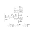
図2は、図1に示した各プロセッサ11での処理動作の概念を説明するための図である。以下の説明では、1つの命令コードは8ビットで構成され、後述するグループコードは3ビットで構成されているものとする。
【0014】
図2において、21は命令キューであり、命令コードを複数保持可能なように複数の命令メモリで構成される。命令メモリは、8ビットの記憶領域をそれぞれ有する。
【0015】
命令デコーダ部13は、グループレジスタ22と命令デコーダ回路23とを有する。グループレジスタ22は、グループコードを記憶するレジスタであり、3ビットの記憶領域を有する。命令デコーダ回路23は、グループコードを参照して命令コードをデコードし、デコード結果に応じた制御処理を行う。24−i(iは添え字であり、i=1〜n(nは任意の自然数))は、図1に示した演算器14に相当する演算器である。
【0016】
ここで、グループコードは、プロセッサ11にて実行可能な処理に係る入力命令を所定の規則に従って分類したグループを指定するものである。グループコードは、グループ毎に互いに異なる値である。
【0017】
入力命令は、例えばシフト演算、ビット演算を含む加減乗除等の四則演算命令、データマッチング等に用いられるWTA演算命令、バースト演算命令、レジスタ操作命令、メモリ制御命令、フロー制御命令、スカラー命令等に分類してグループ化される。各入力命令の命令コードは、グループ内にて互いに異なっていれば良く、グループが異なる場合には同一の命令コードが存在しても良い。つまり、1つの命令コードによりグループが互いに異なる複数の命令を表現することができる。
【0018】
また、入力命令には、何れのグループにも属しない(グループに依存しない)グローバル命令がある。グローバル命令は、例えば、グループコードを変更するためのグループ変更命令、直後の1命令だけグループコードを変更するためのグループ一時変更命令、予め割り当てた任意の命令を実行するためのエイリアス実行命令等がある。
【0019】
次に、動作について説明する。
命令デコーダ回路23は、命令キュー21の命令メモリから1バイト(8ビット)ずつ命令コードICDを読み出す。命令デコーダ回路23は、読み出した命令コードICDにグループレジスタ22より供給されるグループコードGRを付加してデコードする。つまり、命令デコード回路23は、3ビットのグループコードGR及び8ビットの命令コードからなる11ビットのコード(以下、「内部命令コード」とも称す。)をデコードする。
【0020】
デコードの結果、通常の命令、例えば四則演算命令等である場合には、命令デコーダ回路23は、当該命令に応じて制御信号INSを各演算器24−iに供給する。また、デコードの結果、グループコードの変更に係る命令、例えばグループ(一時)変更命令等である場合には、命令デコーダ回路23は、当該命令により指定される変更後のグループコードGRSをグループレジスタ22に書き込む。
【0021】
図3は、命令デコーダ部13の構成例を示すブロック図である。
図3において、31は命令コードを保持する命令メモリ、32は命令デコーダ部13による制御に応じて各種演算処理を行う演算器である。
命令デコーダ部13は、命令ビット連結部33、エイリアス命令デコーダ34、エイリアス命令レジスタ35−j(jは添え字であり、jは任意の自然数)、第1のセレクタ36、グループ変更命令デコーダ37、通常命令デコーダ38、エイリアス変更命令デコーダ39、複数サイクル命令ステートレジスタ40、グループレジスタ41、第2のセレクタ42、グループ一時記憶レジスタ43を含み構成される。
【0022】
命令ビット連結部33は、命令メモリ31から命令コードを1バイトずつ読み出す。また、命令ビット連結部33は、過去に入力された命令コードに基づいて設定され、グループ一時記憶レジスタ43に保持されているグループコードを、命令メモリ31から読み出した命令コードに連結し(付加し)内部命令コードとして出力する。
【0023】
エイリアス命令デコーダ34は、命令ビット連結部33より供給される内部命令コードが、当該内部命令コードをエイリアス命令のコードに置き換えるエイリアス実行命令であるか否かを判断する。判断の結果、エイリアス実行命令である場合には、エイリアス命令デコーダ34は、内部命令コードのグループコードに対応するエイリアス命令レジスタ35−jからエイリアス命令(置き換える内部命令コード)を読み出して出力する。
【0024】
エイリアス命令レジスタ35−jは、グループ毎に設けられており、エイリアス命令として割り当てた他グループの命令の内部命令コードがそれぞれ記憶されている。なお、エイリアス命令レジスタ35−jについては、図3に示した例に限らず、例えばすべてのグループでエイリアス命令を共通にするように構成しても良いし、各グループに複数個のエイリアス命令を有するように構成しても良い。
【0025】
第1のセレクタ36は、命令ビット連結部33より供給される内部命令コード、又はエイリアス命令デコーダ34より供給される内部命令コードを選択的に出力する。
【0026】
グループ変更命令デコーダ37は、第1のセレクタ36より供給される内部命令コードがグループ変更命令又はグループ一時変更命令のものであるときには、グループコードを新たなグループコードに変更する。なお、グループ変更命令デコーダ37は、グループ(一時)変更命令に加え、第1のセレクタ36より供給される内部命令コードが予め設定されたグループコードの変更ルールを満足するときには、グループコードを新たなグループコードに変更するようにしても良い。グループコードの変更ルールは、グループ変更命令デコーダ37内に内部命令コードと変更するグループコードとを関連付けるルックアップテーブル(LUT)44等を設け、設定すれば良い。
【0027】
グループ変更命令デコーダ37は、グループ変更命令又は変更ルールに基づいてグループコードを変更する場合には、新たなグループコードの値をグループレジスタ41に書き込む。これにより、グループレジスタ41にて保持している値が新たなグループコードの値に置き換えられる。さらに、グループレジスタ41が保持している値は、グループ一時記憶レジスタ43に第2のセレクタ42を介して供給され、グループ一時記憶レジスタ43にて保持される。
【0028】
一方、グループ一時変更命令に基づいて、直後の命令のみグループコードを変更する場合には、グループ変更命令デコーダ37は、変更するグループコードの値を第2のセレクタ42を介してグループ一時記憶レジスタ43に供給する。これにより、グループ一時記憶レジスタ43にて保持している値が新たなグループコードの値に置き換えられる。この場合には、グループ変更命令デコーダ37は、グループレジスタ41への書き込みは行わない。
【0029】
通常命令デコーダ38は、第1のセレクタ36より供給される内部命令コードが通常命令(四則演算命令等)のものである場合には、通常のプロセッサと同様にして内部命令コードをデコードし、デコード結果に応じた制御信号を演算器32に出力する。
【0030】
エイリアス変更命令デコーダ39は、第1のセレクタ36より供給される内部命令コードがエイリアス変更命令のものであるときに、エイリアス命令レジスタ35−jの値を書き換える。具体的には、エイリアス変更命令デコーダ39は、内部命令コードに示される変更先のグループコードに対応するエイリアス命令レジスタ35−jの値を、内部命令コードに従い置き換える命令の内部命令コード(グループコード及び命令コード)に書き換える。
【0031】
複数サイクル命令ステートレジスタ40は、エイリアス実行命令により置き換えられたエイリアス命令等が2バイト長以上の命令であるときに、最初の1バイトのみエイリアス命令に置き換え、2バイト目以降はエイリアス命令を無視するように第1のセレクタ36を制御する。
【0032】
すなわち、複数サイクル命令ステートレジスタ40は、最初の1バイトのみエイリアス命令デコーダ34からの内部命令コードを選択し、2バイト目以降は命令ビット連結部33からの内部命令コードを選択するように第1のセレクタ36を制御する。これは、エイリアス命令等が2バイト長以上の命令であるときに、最初の1バイトが命令そのものを示し、2バイト目以降はデータ等であるからである。ここで、グループ変更命令デコーダ37、通常命令デコーダ38、エイリアス変更命令デコーダ39及び複数サイクル命令ステートレジスタ40は、互いに通信を行って動作している。
【0033】
第2のセレクタ42は、クループ変更命令デコーダ37からの制御に応じて、グループレジスタ41が保持しているグループコードの値、又はクループ変更命令デコーダ37より供給されるグループコードの値を選択的にグループ一時記憶レジスタ43に供給する。具体的には、第2のセレクタ42は、グループ一時変更命令に従いグループコードを変更する場合のみ、クループ変更命令デコーダ37からの値を選択して出力し、そうでない場合には、グループレジスタ41からの値を選択して出力する。
なお、図3に示した命令デコーダ部13は、プログラムカウンタ、レジスタ、条件分岐等のフロー制御回路等を含んでいないが、これらを適宜備えるようにしても良い。
【0034】
図4は、グループコードの変更ルールを設定するLUT44の一例を示す図である。
図4に示すようにグループコードの変更ルールは、命令マスクIMk(kは添え字であり、任意の自然数、以下についても同様。)と命令コードICkと変更後のグループコードGCkとを1組として設定する。なお、命令マスクIMk及び命令コードICkは、グループコード(3ビット)と命令コード(8ビット)とに対応する11ビットで設定し、グループコードGCkは、グループコード(3ビット)のみを設定する。
【0035】
命令マスクIMkは、入力される入力命令(内部命令コード)にてマスクするビットを設定する。命令マスクIMkは、マスクするビットには“0”を設定し、そうでないビットには“1”を設定する。
【0036】
命令コードICkは、入力命令と比較する内部命令コードを設定する。命令コードICkは、命令マスクIMkによりマスクされるビットには“0”を設定し、そうでないビットには所望の値を設定する。グループコードGCkは、命令マスクIMkと命令コードICkとで設定される条件に一致した場合に、新たに設定する変更後のグループコードを設定する。
【0037】
例えば、図4に示したように命令マスクIM1、命令コードIC1、グループコードGC1に、値“11110000000”、“10110000000”、“101”がそれぞれ設定されているとき、命令マスクIM1の上位側4ビットが“1”である。したがって、入力命令の上位側4ビットの値と命令コードIC1の上位側4ビットの値とを比較し、一致した場合にはグループコードを“101”に変更する。つまり、入力命令の上位側4ビットの値が“1011”の場合には、グループコードを“101”に変更する。
【0038】
同様に、例えば命令マスクIM2、命令コードIC2、グループコードGC2に、値“11111000000”、“11011000000”、“110”がそれぞれ設定されている場合には、入力命令の上位側5ビットの値が“11011”のときグループコードを“110”に変更する。
【0039】
なお、図4に示したLUT44は一例であり、これに限定されるものではない。例えば、命令マスクと命令コードとの複数の組と1つの変更後のグループコードとを1組として設定し、以前の入力命令を含む複数の入力命令に基づいて、グループコードを変更するようなLUTであっても良い。
【0040】
図5は、入力命令(内部命令コード)が図4に示したグループコードの変更ルールを満足するか否かを判定するためのグループ変更判定回路の一例を示す図であり、当該判定回路は例えばグループ変更命令デコーダ37に設けられる。
【0041】
図5に示すように、判定回路では、入力命令における1つのビットINm(mは添え字であり、mは0〜10の整数、以下についても同様。)と命令マスクMSKにおける1つのビットMBmとの論理積演算が、対応するビット毎に論理積演算(AND)回路51にて行われる。さらに、AND回路51の演算結果と命令コードCODEにおける1つのビットIBmとの排他的否定論理和演算が、対応するビット毎に排他的否定論理和演算(EX−NOR)回路52にて行われる。従属接続されたAND回路53によりすべてのEX−NOR回路52の演算結果が論理積演算され、その演算結果が選択信号SELとして出力される。
【0042】
このように判定回路を構成することで、命令マスクMSKと命令コードCODEとで設定される変更ルールの条件に一致した場合にのみ、選択信号がハイレベルとなり、当該変更ルールで設定されている変更後のグループコードが選択される。
【0043】
以上、詳しく説明したように本実施形態によれば、複数のプロセッサ11を有する並列プロセッサ10にて、各プロセッサ11の命令デコーダ部13は、命令メモリから読み出した命令コードに、過去の命令コードにより定まるグループコードを付加して内部命令コードを生成する。さらに、命令デコーダ部13は、当該内部命令コードに基づいて、読み出した命令コードに割り当てられている複数の命令の中から実行する命令を一意に決定して各種制御を行う。
【0044】
これにより、1つの命令コードに複数の命令を対応させ、短い命令コード長ですべての命令を表現することができ、当該命令コードを保持するプログラムメモリに要する容量の増加を抑制することができる。さらに、同じ命令コードであっても、過去の命令コードにより定まるグループコードに応じて異なる処理を行うことができ、従来に比べて多様かつ高度な処理を実行することが可能になる。
また、任意の命令を割り当てられるエイリアス命令を設けたことにより、1つの命令コードで他のグループの命令を直ちに実行させることができる。
【0045】
なお、上記実施形態では、命令コードは8ビット、グループコードは3ビットとしたが、これは一例であり、本発明はこれに限定されるものではない。
また、上記実施形態は、何れも本発明を実施するにあたっての具体化のほんの一例を示したものに過ぎず、これらによって本発明の技術的範囲が限定的に解釈されてはならないものである。すなわち、本発明はその技術思想、またはその主要な特徴から逸脱することなく、様々な形で実施することができる。
【0046】
【発明の効果】
以上説明したように、本発明によれば、プロセッサにて実行可能なすべての命令に互いに異なる命令コードを対応させずに、1つの命令コードを複数の命令に対応させ、各プロセッサは、命令コードの入力履歴に基づいて、入力される命令コードにより実行する命令を複数の命令の中から一意に決定する。これにより、短い命令コード長ですべての命令を表現することができ、各プロセッサにて命令コードの保持に要するメモリ容量の増加を抑制することができる。また、命令コードが同じであっても、命令コードの入力履歴に応じて異なる命令を実行することができ、多様かつ異なる処理を複数のプロセッサにより並列して実行することができる。
【図面の簡単な説明】
【図1】本発明の実施形態による情報処理装置を適用した並列プロセッサの構成を示すブロック図である。
【図2】本実施形態における各プロセッサでの処理動作の概念を説明するための図である。
【図3】命令デコーダ部の構成例を示すブロック図である。
【図4】グループコードの変更ルールを設定するルックアップテーブルの一例を示す図である。
【図5】グループ変更判定回路の一例を示す図である。
【符号の説明】
10 並列プロセッサ
11 プロセッサ
12 メモリ
13 命令デコーダ部
14 演算器
21 命令キュー
22 グループレジスタ
23 命令デコーダ回路
24 演算器[0001]
TECHNICAL FIELD OF THE INVENTION
The present invention relates to an information processing device, and is particularly suitable for use in an information processing device having a plurality of processors that can operate in parallel on a single chip.
[0002]
[Prior art]
As one of the parallel computers, there is a single instruction multiple data (SIMD) type parallel processor. The SIMD-type parallel processor has a plurality of processors in one chip, and executes one process according to a supplied instruction at the same time in parallel by the plurality of processors.
[0003]
[Problems to be solved by the invention]
Each processor constituting the SIMD type parallel processor is composed of an arithmetic unit and a memory. In the SIMD type processor, one process corresponding to the supplied instruction is executed by all processors in parallel, so that only the data is held in the memory of each processor.
[0004]
Therefore, although the SIMD type processor has a plurality of processors, each processor cannot execute different processing in parallel. For example, when performing data matching or the like, it has not been possible to cause some processors to perform a search process and to cause other processors to perform a detailed comparison process in parallel.
[0005]
Here, in order for a plurality of processors to execute different processes in parallel, it is necessary to store a program (instruction) in the memory of each processor. However, an instruction set used in general-purpose processors in recent years is such that one instruction is composed of 32 bits or 64 bits, and a large storage is required to store a program capable of executing the same processing as that of the general-purpose processor in the memory of each processor. Requires capacity. On the other hand, in order to provide many processors in one chip, it is desirable that the memory capacity of each processor is small.
[0006]
The present invention has been made in view of such circumstances, and while suppressing an increase in the memory capacity required for holding a program in each processor, various and different processes are performed by a plurality of processors provided in one chip. Are executed in parallel.
[0007]
[Means for Solving the Problems]
An information processing apparatus according to the present invention is an information processing apparatus having a plurality of processors on one chip, each of the plurality of processors being capable of independently executing an instruction, and the processor being configured to execute an instruction code input history. And a decoder circuit for uniquely determining an instruction to be executed by the input instruction code from among a plurality of instructions assigned to the instruction code based on the instruction code.
[0008]
According to the present invention, since one instruction code corresponds to a plurality of instructions, the instruction code length can be reduced as compared with a case where different instruction codes correspond to a plurality of instructions, and the same instruction code can be used. Can perform different processing.
[0009]
BEST MODE FOR CARRYING OUT THE INVENTION
Hereinafter, embodiments of the present invention will be described with reference to the drawings.
FIG. 1 is a block diagram illustrating a configuration of a
[0010]
The
The
[0011]
The
The
[0012]
In FIG. 1, the
[0013]
FIG. 2 is a diagram for explaining the concept of the processing operation in each
[0014]
In FIG. 2,
[0015]
The
[0016]
Here, the group code specifies a group in which input instructions related to processing executable by the
[0017]
Input instructions include, for example, four arithmetic operations such as shift operation, addition, subtraction, multiplication and division including bit operations, WTA operation instructions used for data matching, burst operation instructions, register operation instructions, memory control instructions, flow control instructions, scalar instructions, etc. Classified and grouped. The instruction codes of the input instructions need only be different from each other within the group, and if the groups are different, the same instruction code may exist. In other words, a plurality of instructions in different groups can be expressed by one instruction code.
[0018]
The input instructions include a global instruction that does not belong to any group (does not depend on the group). Global instructions include, for example, a group change instruction for changing the group code, a group temporary change instruction for changing the group code by only one immediately following instruction, and an alias execution instruction for executing any pre-assigned instruction. is there.
[0019]
Next, the operation will be described.
The
[0020]
If the result of the decoding is a normal instruction, for example, an arithmetic operation instruction, the
[0021]
FIG. 3 is a block diagram illustrating a configuration example of the
In FIG. 3, reference numeral 31 denotes an instruction memory for holding an instruction code, and 32 denotes an arithmetic unit for performing various arithmetic processes under the control of the
The
[0022]
The instruction
[0023]
The
[0024]
The alias instruction register 35- j is provided for each group, and stores an internal instruction code of an instruction of another group assigned as an alias instruction. The alias instruction register 35- j is not limited to the example shown in FIG. 3, but may be configured so that the alias instruction is common to all groups, or a plurality of alias instructions are assigned to each group. You may comprise so that it may have.
[0025]
The
[0026]
The group
[0027]
When changing a group code based on a group change command or a change rule, the group
[0028]
On the other hand, when the group code is to be changed only for the immediately following instruction based on the group temporary change instruction, the group
[0029]
When the internal instruction code supplied from the
[0030]
The alias
[0031]
The multi-cycle
[0032]
That is, the multi-cycle
[0033]
The
Although the
[0034]
FIG. 4 is a diagram illustrating an example of the
As shown in FIG. 4, the rule for changing the group code is a set of an instruction mask IMk (k is a suffix and an arbitrary natural number, the same applies to the following), an instruction code ICk, and a changed group code GCk. Set. The instruction mask IMk and the instruction code ICk are set with 11 bits corresponding to the group code (3 bits) and the instruction code (8 bits), and the group code GCk is set only with the group code (3 bits).
[0035]
The instruction mask IMk sets bits to be masked by an input instruction (internal instruction code) to be input. The instruction mask IMk sets “0” to bits to be masked and “1” to bits not to be masked.
[0036]
The instruction code ICk sets an internal instruction code to be compared with the input instruction. The instruction code ICk sets “0” to bits masked by the instruction mask IMk, and sets a desired value to bits that are not. The group code GCk sets a new changed group code to be set when the conditions set by the instruction mask IMk and the instruction code ICk match.
[0037]
For example, as shown in FIG. 4, when the values “11111000000”, “10111000000”, and “101” are set in the instruction mask IM1, the instruction code IC1, and the group code GC1, respectively, the upper four bits of the instruction mask IM1 Is “1”. Therefore, the value of the upper 4 bits of the input instruction is compared with the value of the upper 4 bits of the instruction code IC1, and if they match, the group code is changed to “101”. That is, when the value of the upper 4 bits of the input instruction is “1011”, the group code is changed to “101”.
[0038]
Similarly, for example, when the values “11111100000”, “11011100000”, and “110” are set in the instruction mask IM2, the instruction code IC2, and the group code GC2, respectively, the value of the upper 5 bits of the input instruction is “ At the time of “11011”, the group code is changed to “110”.
[0039]
Note that the
[0040]
FIG. 5 is a diagram illustrating an example of a group change determination circuit for determining whether an input instruction (internal instruction code) satisfies the group code change rule illustrated in FIG. 4. The group
[0041]
As shown in FIG. 5, in the determination circuit, one bit INm (m is a suffix, m is an integer of 0 to 10 and the same applies to the following) in the input instruction and one bit MBm in the instruction mask MSK are used. AND operation is performed by the AND
[0042]
By configuring the determination circuit in this manner, only when the condition of the change rule set by the instruction mask MSK and the instruction code CODE matches, the selection signal becomes high level, and the change set by the change rule is changed. The later group code is selected.
[0043]
As described above in detail, according to the present embodiment, in the
[0044]
As a result, a plurality of instructions can be made to correspond to one instruction code, and all the instructions can be expressed with a short instruction code length, thereby suppressing an increase in the capacity required for the program memory holding the instruction code. Further, even with the same instruction code, different processing can be performed according to the group code determined by the previous instruction code, and various and advanced processing can be executed as compared with the conventional art.
Further, by providing an alias instruction to which an arbitrary instruction can be assigned, it is possible to immediately execute another group of instructions with one instruction code.
[0045]
In the above embodiment, the instruction code has 8 bits and the group code has 3 bits. However, this is an example, and the present invention is not limited to this.
Further, each of the embodiments described above is merely an example of a concrete example for carrying out the present invention, and the technical scope of the present invention should not be interpreted in a limited manner. That is, the present invention can be implemented in various forms without departing from the technical idea or the main features.
[0046]
【The invention's effect】
As described above, according to the present invention, one instruction code is made to correspond to a plurality of instructions without making different instruction codes correspond to all the instructions executable by the processor. , An instruction to be executed by an input instruction code is uniquely determined from a plurality of instructions. Thus, all instructions can be expressed with a short instruction code length, and an increase in the memory capacity required to hold the instruction code in each processor can be suppressed. Even if the instruction codes are the same, different instructions can be executed according to the input history of the instruction codes, and various and different processes can be executed in parallel by a plurality of processors.
[Brief description of the drawings]
FIG. 1 is a block diagram illustrating a configuration of a parallel processor to which an information processing device according to an embodiment of the present invention has been applied.
FIG. 2 is a diagram for explaining a concept of a processing operation in each processor in the embodiment.
FIG. 3 is a block diagram illustrating a configuration example of an instruction decoder unit.
FIG. 4 is a diagram showing an example of a look-up table for setting a group code change rule.
FIG. 5 is a diagram illustrating an example of a group change determination circuit.
[Explanation of symbols]
Claims (5)
上記複数のプロセッサは、それぞれが独立して命令実行可能であり、
上記プロセッサは、命令コードの入力履歴に基づいて、命令コードに割り当てられている複数の命令の中から、入力される命令コードにより実行する命令を一意に決定するデコーダ回路をそれぞれ有することを特徴とする情報処理装置。An information processing apparatus having a plurality of processors on one chip,
The plurality of processors are each capable of executing instructions independently,
The processor has a decoder circuit that uniquely determines an instruction to be executed by an input instruction code from a plurality of instructions assigned to the instruction code based on an input history of the instruction code. Information processing device.
上記プロセッサにて実行可能な命令は、複数の命令群に分類されるとともに、同一の命令群内では互いに異なるように命令コードが各命令に付与され、
上記プロセッサは、命令コードの入力履歴に基づいて入力される命令コードに対する命令群を選択して、入力される命令コードにより実行する命令を一意にそれぞれ決定することを特徴とする情報処理装置。An information processing apparatus having a plurality of processors each capable of independently executing instructions on one chip,
The instructions executable by the processor are classified into a plurality of instruction groups, and instruction codes are assigned to the respective instructions so as to be different from each other in the same instruction group.
An information processing apparatus, wherein the processor selects an instruction group for an input instruction code based on an input history of the instruction code, and uniquely determines an instruction to be executed by the input instruction code.
Priority Applications (2)
| Application Number | Priority Date | Filing Date | Title |
|---|---|---|---|
| JP2003039741A JP3837386B2 (en) | 2003-02-18 | 2003-02-18 | Information processing device |
| US10/779,801 US20040162965A1 (en) | 2003-02-18 | 2004-02-18 | Information processing unit |
Applications Claiming Priority (1)
| Application Number | Priority Date | Filing Date | Title |
|---|---|---|---|
| JP2003039741A JP3837386B2 (en) | 2003-02-18 | 2003-02-18 | Information processing device |
Publications (2)
| Publication Number | Publication Date |
|---|---|
| JP2004252556A true JP2004252556A (en) | 2004-09-09 |
| JP3837386B2 JP3837386B2 (en) | 2006-10-25 |
Family
ID=32844479
Family Applications (1)
| Application Number | Title | Priority Date | Filing Date |
|---|---|---|---|
| JP2003039741A Expired - Fee Related JP3837386B2 (en) | 2003-02-18 | 2003-02-18 | Information processing device |
Country Status (2)
| Country | Link |
|---|---|
| US (1) | US20040162965A1 (en) |
| JP (1) | JP3837386B2 (en) |
Cited By (1)
| Publication number | Priority date | Publication date | Assignee | Title |
|---|---|---|---|---|
| JP2009048637A (en) * | 2007-08-15 | 2009-03-05 | Nvidia Corp | Shared readable and writable global values in graphics processor unit pipeline |
Families Citing this family (2)
| Publication number | Priority date | Publication date | Assignee | Title |
|---|---|---|---|---|
| US9069547B2 (en) * | 2006-09-22 | 2015-06-30 | Intel Corporation | Instruction and logic for processing text strings |
| GB2489914B (en) | 2011-04-04 | 2019-12-18 | Advanced Risc Mach Ltd | A data processing apparatus and method for performing vector operations |
Family Cites Families (1)
| Publication number | Priority date | Publication date | Assignee | Title |
|---|---|---|---|---|
| US6697939B1 (en) * | 2000-01-06 | 2004-02-24 | International Business Machines Corporation | Basic block cache microprocessor with instruction history information |
-
2003
- 2003-02-18 JP JP2003039741A patent/JP3837386B2/en not_active Expired - Fee Related
-
2004
- 2004-02-18 US US10/779,801 patent/US20040162965A1/en not_active Abandoned
Cited By (1)
| Publication number | Priority date | Publication date | Assignee | Title |
|---|---|---|---|---|
| JP2009048637A (en) * | 2007-08-15 | 2009-03-05 | Nvidia Corp | Shared readable and writable global values in graphics processor unit pipeline |
Also Published As
| Publication number | Publication date |
|---|---|
| US20040162965A1 (en) | 2004-08-19 |
| JP3837386B2 (en) | 2006-10-25 |
Similar Documents
| Publication | Publication Date | Title |
|---|---|---|
| KR101766183B1 (en) | Functional unit having tree structure to support vector sorting algorithm and other algorithms | |
| KR100346515B1 (en) | Temporary pipeline register file for a superpipe lined superscalar processor | |
| JP2011090592A (en) | Information processing apparatus and instruction decoder for the same | |
| US20140047218A1 (en) | Multi-stage register renaming using dependency removal | |
| TWI739754B (en) | Vector arithmetic instruction | |
| JP2006018453A (en) | Semiconductor device | |
| US7441099B2 (en) | Configurable SIMD processor instruction specifying index to LUT storing information for different operation and memory location for each processing unit | |
| EP1193594B1 (en) | Register renaming apparatus and processor | |
| JP2023533795A (en) | Erasing register data | |
| JP3837386B2 (en) | Information processing device | |
| JP3578267B2 (en) | A hardware device that executes a programmable instruction based on a micro instruction | |
| JP2003241960A (en) | Processor, and computation instruction processing method and computation control method therein | |
| US20090070559A1 (en) | Data processing circuit wherein functional units share read ports | |
| JP5327432B2 (en) | Signal processor and semiconductor device | |
| JP3454393B2 (en) | Data processing device | |
| JPH1091593A (en) | Data processor provided with microprocessor and optional calculation unit | |
| JP5245617B2 (en) | Register control circuit and register control method | |
| JP5263498B2 (en) | Signal processor and semiconductor device | |
| US5774740A (en) | Central processing unit for execution of orthogonal and non-orthogonal instructions | |
| JP5311008B2 (en) | Signal processor and semiconductor device | |
| WO2011086808A1 (en) | Information processing device | |
| JP5263497B2 (en) | Signal processor and semiconductor device | |
| JP2024087606A (en) | Processor, instruction execution program and information processing device | |
| JPH10240528A (en) | Risc computer | |
| CN118963237A (en) | Control system, control method, medium and terminal based on programmable logic array |
Legal Events
| Date | Code | Title | Description |
|---|---|---|---|
| A977 | Report on retrieval |
Free format text: JAPANESE INTERMEDIATE CODE: A971007 Effective date: 20050425 |
|
| A131 | Notification of reasons for refusal |
Free format text: JAPANESE INTERMEDIATE CODE: A131 Effective date: 20050621 |
|
| A521 | Request for written amendment filed |
Free format text: JAPANESE INTERMEDIATE CODE: A523 Effective date: 20050822 |
|
| A131 | Notification of reasons for refusal |
Free format text: JAPANESE INTERMEDIATE CODE: A131 Effective date: 20051004 |
|
| A521 | Request for written amendment filed |
Free format text: JAPANESE INTERMEDIATE CODE: A523 Effective date: 20051205 |
|
| TRDD | Decision of grant or rejection written | ||
| A01 | Written decision to grant a patent or to grant a registration (utility model) |
Free format text: JAPANESE INTERMEDIATE CODE: A01 Effective date: 20060704 |
|
| A61 | First payment of annual fees (during grant procedure) |
Free format text: JAPANESE INTERMEDIATE CODE: A61 Effective date: 20060731 |
|
| R150 | Certificate of patent or registration of utility model |
Free format text: JAPANESE INTERMEDIATE CODE: R150 |
|
| LAPS | Cancellation because of no payment of annual fees |