JP2004239929A - Color filter for translucent liquid crystal display device - Google Patents
Color filter for translucent liquid crystal display device Download PDFInfo
- Publication number
- JP2004239929A JP2004239929A JP2003025715A JP2003025715A JP2004239929A JP 2004239929 A JP2004239929 A JP 2004239929A JP 2003025715 A JP2003025715 A JP 2003025715A JP 2003025715 A JP2003025715 A JP 2003025715A JP 2004239929 A JP2004239929 A JP 2004239929A
- Authority
- JP
- Japan
- Prior art keywords
- liquid crystal
- display device
- crystal display
- color filter
- transparent portion
- Prior art date
- Legal status (The legal status is an assumption and is not a legal conclusion. Google has not performed a legal analysis and makes no representation as to the accuracy of the status listed.)
- Pending
Links
Images


Classifications
-
- H—ELECTRICITY
- H01—ELECTRIC ELEMENTS
- H01J—ELECTRIC DISCHARGE TUBES OR DISCHARGE LAMPS
- H01J1/00—Details of electrodes, of magnetic control means, of screens, or of the mounting or spacing thereof, common to two or more basic types of discharge tubes or lamps
- H01J1/02—Main electrodes
- H01J1/13—Solid thermionic cathodes
- H01J1/14—Solid thermionic cathodes characterised by the material
Landscapes
- Optical Elements Other Than Lenses (AREA)
- Optical Filters (AREA)
- Liquid Crystal (AREA)
Abstract
Description
【0001】
【発明の属する技術分野】
本発明は、液晶表示装置用カラーフィルタの製造方法に関するものであり、特に、一画素中の着色画素が、一画素中の光透過領域に形成された着色層と、光反射領域に形成され、透明部を有する着色層とで構成されるカラーフィルタの該透明部を精度よく製造した半透過型液晶表示装置用カラーフィルタに関する。
【0002】
【従来の技術】
液晶表示装置は自発光型の表示装置ではないので、その表示には他からの光を必要とし、例えば、その後方にバックライトを設け、後方からの光によって表示を行っている。このような液晶表示装置は透過型液晶表示装置と称され、主に屋内のような暗い環境下で用いられる。
また、例えば、その後方に光反射層を設け、液晶表示装置を観視する際の周囲からの外光によって表示を行う液晶表示装置がある。このような液晶表示装置は反射型液晶表示装置と称され、主に屋外のような周囲が明るい環境下で用いられる。
【0003】
上記透過型液晶表示装置においては、その後方に設けられたバックライトからの光はカラーフィルタの着色画素を透過し、液晶表示装置が観視される前方の外部へ射出されるようになっている。
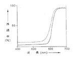
この際の着色画素の分光透過率は、例えば、図5における実線で示すように、赤色の着色画素の分光透過率は波長400〜600nmにおいては透過率が低く、波長600〜700nmにおいては透過率が高いものが好ましいものである。
【0004】
図6は、従来法の反射型液晶表示装置の一例を断面で示す説明図であるが、図6に示すように、反射型液晶表示装置(60)は、対向基板(68)、液晶(65)、カラーフィルタ(69)などで構成されている。図6において、対向基板(68)は、画素表示に必要な駆動素子(図示せず)や光拡散反射性の電極層(66)などが基板(67)上に形成されたもので構成されている。
また、カラーフィルタ(69)は、ガラス基板(61)、着色画素(62)、オーバーコート層(63)、透明電極層(64)などで構成されている。
【0005】
図6において、外光(L1)は着色画素(62)を通過し色光となり、光拡散反射性の電極層(66)にて反射され、再び着色画素(62)を通過して、外部へ反射光(L2)として射出されるようになっている。
このような反射型液晶表示装置用カラーフィルタの着色画素(62)の色濃度は、透過型液晶表示装置用カラーフィルタのカラーフィルタ画素の色濃度より低い色濃度のものである。
【0006】
これは、上記のように外部からの光は、入射の際と反射の際の2回にわたり赤色の着色画素を透過し、外部へ射出されるので、例えば、図5における点線で示すように、赤色の着色画素の分光透過率は波長400〜600nmにおいて透過率がやや高く、波長600〜700nmにおいても透過率がやや高いものを用いることにより、実線で示す透過型に用いられる赤色の着色画素の分光透過率と同様の効果が得られるようにしているものである。
そして、このような点線で示すような分光透過率を有する着色画素の形成は、例えば、着色画素に含まれる顔料の含有量を少なくすることにより行われている。
【0007】
さて、液晶表示装置用カラーフィルタの着色画素の形成は、種々な方法により行われているが、感光性樹脂組成物に顔料を分散させた感光性着色樹脂組成物(着色フォトレジスト)を材料として用い、フォトリソグラフィー法により着色画素を形成する顔料分散法が広く採用されている。
【0008】
この顔料分散法、すなわち、着色フォトレジストを用いフォトリソグラフィー法により、上記のような反射型液晶表示装置用カラーフィルタの着色画素を形成する場合には、画素の色濃度を低くするため、その着色画素に含まれる顔料の含有量を少なくしたり、または、着色画素の厚さを薄く形成する手段が用いられている。
【0009】
上記透過型液晶表示装置は、主に屋内のような暗い環境下で用いられるものであり、屋外のような周囲が明るい環境下では、その表示が見にくいといった欠点がある。また、上記反射型液晶表示装置は、主に屋外のような周囲が明るい環境下で用いられるものであり、屋内のような暗い環境下では、その表示が見にくいといった欠点がある。
【0010】
このような透過型液晶表示装置、反射型液晶表示装置に対し、半透過型液晶表示装置と称される液晶表示装置は、1基の液晶表示装置において透過型と反射型の両機能を兼ね備えた液晶表示装置である。
この半透過型液晶表示装置は、屋外のような非常に明るい環境下でも、屋内のような暗い環境下でも用いることができるものであり、モバイル機器に用いられる液晶表示装置として期待されている液晶表示装置である。
【0011】
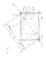
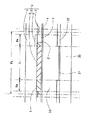
図3は、半透過型液晶表示装置に用いられるカラーフィルタの一例を示したものであり、一画素に対応する部位を拡大して示す平面図である。また、図4は、図3に示す半透過型液晶表示装置用カラーフィルタを用いた半透過型液晶表示装置の一画素の部分を示す断面説明図である。図3におけるX−X’線の断面が、図4に示す半透過型液晶表示装置用カラーフィルタ(30)の断面に相当する。
【0012】
図3、及び図4に示すように、この半透過型液晶表示装置は、半透過型液晶表示装置用カラーフィルタ(30)、半透過型液晶表示装置用カラーフィルタ上に形成された透明電極(14)、液晶(50)、TFT素子(図示せず)などが形成されたTFT基板(40)、TFT基板上に形成された透明電極(41)及び反射電極(42)で構成されている。
【0013】
半透過型液晶表示装置用カラーフィルタ(30)は、ガラス基板(11)上にブラックマトリックス(12)、着色画素(13)が形成されたものである。また、透明電極(41)及び反射電極(42)はTFT素子のドレイン電極と接続されている。
1画素の領域(Px)はブラックマトリックス(12)を除くと、光透過領域(Tr)と光反射領域(Re)とで構成されている。
光透過領域(Tr)は、透過型液晶表示装置として機能する領域であり、光反射領域(Re)は、反射型液晶表示装置として機能する領域である。
【0014】
1画素の領域(Px)内の着色層(15)及び透明部を有する着色層(16)は、同一の着色層形成材料を用いて設けられた同一厚さの着色層である。図4にては、説明上、左斜線と右斜線で表記してある。また、図4中、反射電極(42)の両端の上方が着色層(15)と透明部を有する着色層(16)との境界であり、鎖線で表記してある。
着色画素(13)の光透過領域(Tr)には、その全領域に厚さD1の均一な着色層(15)が形成され、また、光反射領域(Re)には、外光が入反射する透明部(17)を有する着色層(16)が形成されている。
【0015】
すなわち、1画素の領域(Px)内では、光透過領域(Tr)の均一な着色層(15)と、光反射領域(Re)の透明部を有する着色層(16)とで着色画素(13)が構成されている。
そして、この透明部を有する着色層(16)の厚さは、その平均厚さ(D2)で表される。尚、平坦性をもたせるため着色層(16)の透明部(17)には、無色透明な樹脂を充填するのが一般的である。
【0016】
図4に示す、厚さD1を有する均一な着色層(15)の分光透過率は図5に実線で示すような、例えば、赤色の着色画素の分光透過率は波長400〜600nmにおいては透過率が低く、波長600〜700nmにおいては透過率が高い透過型液晶表示装置に好適な分光透過率を有する。
光透過領域(Tr)においては白太矢印(A)で示すバックライトからの白色光が、TFT基板(40)、透明電極(41)、液晶(50)、透明電極(14)を経て着色画素(13)の光透過領域(Tr)の着色層(15)を通過し色光となり白細矢印(a)で示すように、外部へ射出するようになっている。
従って、この半透過型液晶表示装置のバックライトを点灯し透過型液晶表示装置として使用した際には、透過型液晶表示装置として優れた明度、彩度を有する透過カラー表示をする。
【0017】
また、この半透過型液晶表示装置のバックライトを消灯し、屋外のような非常に明るい環境下で反射型液晶表示装置として使用した際には、光反射領域(Re)において、斜線太矢印(B)で示す周囲からの外光が、ガラス基板(11)、平均厚さ(D2)の、透明部を有する着色層(16)を通過し色光となり反射電極(42)にて反射され、斜線細矢印(b)で示すように、再び外部へ射出するようになっている。
【0018】
この際の反射光は、平均厚さ(D2)の透明部を有する着色層(16)を2回にわたり通過しているので、その分光透過率は図5に点線で示すような、赤色の着色画素の分光透過率は波長400〜600nmにおいて透過率がかなり高く、波長600〜700nmにおいても透過率が高い、すなわち、反射型液晶表示装置の分光透過率として好適な分光透過率を有するものとなる。
【0019】
このような半透過型液晶表示装置用カラーフィルタを用いることにより、透過型液晶表示装置としての優れた明度、彩度を有する透過カラー表示をし、また、反射型液晶表示装置として暗くならず、優れた明度、彩度を有する反射カラー表示をすることが可能となる。
【0020】
しかし、図3、及び図4に示すような、着色層(15)と透明部を有する着色層(16)とで着色画素が構成される半透過型液晶表示装置用カラーフィルタにおいては、透明部(17)の面積が不均一になり易く、透明部(17)の面積が不均一なカラーフィルタを液晶表示装置に用いると、画面に色むらがでやすいといった問題が発生している。
透明部(17)の大きさは、一画素が、例えば、100μm×300μm程度の際には直径15〜50μm程度のものである。
【0021】
透明部(17)の大きさが大きい場合には、比較的精度よく透明部(17)を形成することができ、透明部(17)の面積は略均一なものとなるが、透明部(17)の大きさが小さくなるに従い、精度よく形成することができず、透明部(17)の面積が不均一なものとなる。
液晶表示装置の画面内で透明部(17)の面積が不均一であると、図4に示す透明部を有する着色層(16)の平均厚さ(D2)が不均一なものとなり、これが画面に色むらとなって現れる。
すなわち、半透過型液晶表示装置を反射型液晶表示装置として使用した際に、画面に色むらとなって現れ、表示品質が劣化したものとなる。
【0022】
このように、透明部(17)の直径が小さい場合に解像度が悪くなり、透明部(17)の面積が不均一になる要因の一つとして、使用する着色フォトレジストの解像度があげられている。液晶表示装置用カラーフィルタの着色画素の形成に用いる着色フォトレジストには顔料が分散されており、一画素の大きさは数10μm以上の画素を形成するのに好適なものである。
【0023】
また、他の要因としては、露光装置、及び露光方法があげられている。液晶表示装置用カラーフィルタを顔料分散法によって大量に製造する際には、一基の液晶表示装置に対応したカラーフィルタを大型ガラス基板に多面付けした状態で製造する。例えば、対角14インチのカラーフィルタを550mm×650mm程度の大サイズのガラス基板に4面付けして製造する。
この際には、カラーフィルタの多面全体が描画されている略大型ガラス基板大の一枚のフォトマスクを用いて、大型ガラス基板上に塗布されたフォトレジストに一回の露光により多面全体を露光する方法が採用されている。この露光法は、一括露光法と称している方法である。
【0024】
これは、IC製造におけるウエファー基板上に塗布されたフォトレジストに、例えば、一個のICが描画されているフォトマスクを用いて、ウエファー基板上の位置を変えて、多回数の露光をし、多数のICを面付けした状態に露光する方法、すなわちステップアンドリピート露光法に対する称しかたである。
従来、液晶表示装置に用いられるカラーフィルタを製造する際の露光法として、コストの面から一括露光法が広く採用されている。
一括露光法による画素形成においては、面内及び面間に画素の不均一が発生し易いものであるが、大型ガラス基板のサイズが、例えば、550mm×650mm程度から650mm×850mm程度へと大サイズ化するに伴い、画素の不均一が助長されたものとなる。
【0025】
また、この一括露光法において、露光装置内では、ガラス基板にフォトマスクが密着することによって生じるキズを防止するため、また、フォトマスクに塵埃が付着した際に画素が欠陥となってしまうのを防止するため着色フォトレジストが塗布されたガラス基板と、略ガラス基板大のフォトマスクとは、例えば、数10μmの間隙を保ってのプロキシミティ(近接)露光を行っている。
着色画素のように、画素の大きさが、例えば、100μm×300μm程度である場合、このプロキシミティ(近接)露光による解像度の劣化は顕著でないが、画素の大きさが、例えば、透明部の大きさのように数10μm以下のものになると、露光光の回折による解像度への影響が顕著なものとなってくる。
【0026】
また、ガラス基板とフォトマスクとのプロキシミティ(近接)の間隔の均一性も、露光装置の大型化に伴いフォトマスクの弛みなどによって、次第に大きくなり画素の不均一が助長されてくる。
【0027】
また、上記、着色層(15)と透明部を有する着色層(16)とで着色画素が構成される半透過型液晶表示装置用カラーフィルタにおいては、着色画素の微小化に伴い、或いは、カラー表示において、より微小な色度の制御をする上で透明部の直径としては、より小さな、例えば、10μm以下といった小さな直径を有する透明部が要望されるようになってきた。
【0028】
【発明が解決しようとする課題】
本発明は、上記問題を解決するためになされたものであり、着色画素が光透過領域に形成された着色層と、光反射領域に形成され、透明部を有する着色層とで構成される半透過型液晶表示装置用カラーフィルタであって、透明部の面積が均一な、また、透明部の面積をより小さく均一にすることが可能な半透過型液晶表示装置用カラーフィルタ、すなわち、透明部の面積が不均一であることに起因する液晶表示装置の画面の色むらを解消した、また、より小さな着色画素の透明部への対応、或いは、より微小な色度の制御を可能とする半透過型液晶表示装置用カラーフィルタを提供することを課題とするものである。
【0029】
【課題を解決するための手段】
本発明は、一画素中の着色画素が、光透過領域に形成された着色層と、光反射領域に形成され、透明部を有する着色層とで構成される半透過型液晶表示装置用カラーフィルタであって、基板上に形成された、矩形の開口部を有するブラックマトリックスの少なくとも該開口部の一隅に、該開口部の一隅のブラックマトリックス端部を二辺とし、該開口部内の着色層端部を他の一辺とする三角形状の透明部を設けたことを特徴とする半透過型液晶表示装置用カラーフィルタである。
【0030】
また、本発明は、上記発明による半透過型液晶表示装置用カラーフィルタにおいて、前記透明部を開口部の対角する二隅に設けたことを特徴とする半透過型液晶表示装置用カラーフィルタである。
【0031】
また、本発明は、上記発明による半透過型液晶表示装置用カラーフィルタにおいて、前記透明部の面積が、カラーフィルタを構成する着色層の色毎に異なる面積であることを特徴とする半透過型液晶表示装置用カラーフィルタである。
【0032】
【発明の実施の形態】
以下に本発明による半透過型液晶表示装置用カラーフィルタを、その一実施形態に基づいて説明する。
図1は、本発明による半透過型液晶表示装置用カラーフィルタの一実施例を示したものであり、一画素に対応する部位を拡大して示す平面図である。また、図2は、図1に示す半透過型液晶表示装置用カラーフィルタを用いた半透過型液晶表示装置の一画素の部分を示す断面説明図である。図1におけるX−X’線の断面が、図2に示す半透過型液晶表示装置用カラーフィルタ(10)の断面に相当する。
【0033】
図1、及び図2に示すように、この半透過型液晶表示装置は、半透過型液晶表示装置用カラーフィルタ(10)、半透過型液晶表示装置用カラーフィルタ上に形成された透明電極(4)、液晶(50)、TFT素子(図示せず)などが形成されたTFT基板(20)、TFT基板上に形成された透明電極(21)及び反射電極(22)で構成されている。
【0034】
半透過型液晶表示装置用カラーフィルタ(10)は、ガラス基板(1)上にブラックマトリックス(2)、着色画素(3)が形成されたものである。また、透明電極(21)及び反射電極(22)はTFT素子のドレイン電極と接続されている。
1画素の領域(Px)はブラックマトリックス(2)を除くと、光透過領域(Tr)と光反射領域(Re)とで構成されている。
光透過領域(Tr)は、透過型液晶表示装置として機能する領域であり、光反射領域(Re)は、反射型液晶表示装置として機能する領域である。
【0035】
1画素の領域(Px)内の着色層(5)及び透明部を有する着色層(6)は、同一の着色層形成材料を用いて設けられた同一厚さの着色層である。図2にては、説明上、左斜線と右斜線で表記してある。また、図2中、透明電極(21)の両端の上方が着色層(5)と透明部を有する着色層(6)との境界であり、鎖線で表記してある。
着色画素(3)の光透過領域(Tr)には、その全領域に厚さの均一な着色層(5)が形成され、また、光反射領域(Re)には、外光が入反射する透明部(7)を有する着色層(6)が形成されている。
【0036】
ガラス基板(1)上に形成されたブラックマトリックス(2)は、遮光性を有するマトリックス状のものであり、遮光性を有するマトリックス以外の部分が開口部となっている。着色画素(3)はブラックマトリックス(2)が形成されたガラス基板(1)上に、その周縁部をブラックマトリックスに重ねるように形成されている。
ブラックマトリックスは、カラーフィルタの着色画素の位置を定め、大きさを均一なものとし、また、表示装置に用いられた際に、好ましくない光を遮蔽し、表示装置の画像をムラのない均一な、且つコントラストを向上させた画像にする機能を有している。
【0037】
本発明における透明部(7)は、図1中、開口部の左上部の一隅に設けられている。その形状は三角形であり、開口部の一隅のブラックマトリックス端部(d、e)を二辺とし、開口部内の着色層端部(透明部を有する着色層(6)の開口部内の端部)(c)を他の一辺とする三角形状である。
この際の、透明部を有する着色層(6)は、この開口部の一隅では、その周縁部をブラックマトリックスに重ねることなく、透明部(7)を設けるために開口部内に周縁部(端部)(着色層端部(c))を有するものとなっている。
【0038】
着色フォトレジストを用いフォトリソグラフィー法によって形成される透明部の面積の精度は、本発明における三角形状の透明部では、既に形成されているブラックマトリックス端部(d、e)を二辺とし、残る一辺の着色層端部(c)をフォトリソグラフィー法によって形成するので、着色層端部(c)の加工精度、すなわち、着色層端部(c)の一辺の、略、図1にX−X’で示す方向、いわば一方向の加工精度により定まる。
一方、図3に示す円形状の透明部では、円周の加工精度、図3にx、yで示す方向、いわば二方向の加工精度により定まる。従って、本発明における三角形状の透明部の面積は、円形状の透明部の面積に比較し、略2倍の精度を有するものとなる。
【0039】
フォトレジストを用いフォトリソグラフィー法によって画素を形成する工程が、解像度の点で十分に余裕のある工程であると、このような精度の差は顕著に表れてこないが、前記のように、現状の液晶表示装置用カラーフィルタのフォトリソグラフィー工程においては、透明部の直径が小さくなるのに従い透明部の面積を精度よく形成することができず、不均一なものとなってしまうといった解像度であるので、上記略2倍の精度向上は透明部の面積の均一化に顕著な効果を及ぼす。
また、透明部の面積の精度向上は、着色画素の微小化に伴って要望されているより小さな透明部の形成が可能となり、或いは、カラー表示において、より微小な色度の制御をする上で要望されているより小さな透明部の形成が可能となる。
【0040】
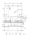
図7(a)は、図1に示すブラックマトリックス(2)と着色画素(3)の位置関係を着色画素の配列の点から表した説明図である。図1は、一画素を拡大した平面図であるが、図7(a)は、例えば、赤色の着色画素(3)の連続した三画素の配列を表している。
図7(a)に示すように、着色画素(3)はストライプ状であり、その両端がブラックマトリックス(2)に重なるように形成されている。着色画素(3)は、三角形状の透明部(7)を設けるために開口部(8)内に着色層端部(c)を有した切り欠きストライプ状である。
【0041】
図7(b)は、本発明における透明部(7)の他の例を示す説明図である。図7(b)に示すように、透明部(7)は、開口部(8)の対角する二隅に設けられた第一透明部(7a)と第二透明部(7b)で構成されたものである。
透明部(7)を、このように対角する二隅に等分して設けることにより、既に形成されたブラックマトリックス(2)に対し、着色画素(3)をx、y方向に位置合わせして形成する際の位置合わせにバラツキがあっても、そのバラツキを相殺し透明部(7)の面積は一定に保たれたものとなる。
【0042】
図7(c)は、本発明における透明部(7)の他の第二例を示す説明図である。図7(b)に示すように、この例は、ブラックマトリックス(2)に対し、緑色の着色画素(3G)、赤色の着色画素(3R)、青色の着色画素(3B)が設けられたものである。緑色の着色画素(3G)の透明部(7c)と、赤色の着色画素(3R)の透明部(7d)と、青色の着色画素(3B)の透明部(7e)とは、各々その面積を異にしている。
これは、図5に赤色を例にして示した、前記反射型液晶表示装置用カラーフィルタの分光透過率として好適な、図中点線で示す分光透過率は各々の色によって異にした方が好ましい際に採用される。また、各々異にした面積は、液晶表示装置とし色再現をする上で緑色、赤色、青色のバランスをとる際に、各々の色によって異にした方が好ましい際に採用される。
図7においては、着色画素としてストライプ状のものを示したが、着色画素は開口部毎に独立した矩形状のものでもよい。
【0043】
上記のように、本発明による半透過型液晶表示装置用カラーフィルタは、着色フォトレジストを用いフォトリソグラフィー法によって製造する、現状の材料、装置、及び方法を大幅に変更することなく製造でき、透明部の面積が均一な、また、透明部の面積をより小さく均一にすることが可能な半透過型液晶表示装置用カラーフィルタとなる。
【0044】
【発明の効果】
本発明は、基板上に形成された、矩形の開口部を有するブラックマトリックスの少なくとも開口部の一隅に、開口部の一隅のブラックマトリックス端部を二辺とし、開口部内の着色層端部を他の一辺とする三角形状の透明部を設けた半透過型液晶表示装置用カラーフィルタであるので、透明部の面積が均一な、また、透明部の面積をより小さく均一にすることが可能な半透過型液晶表示装置用カラーフィルタ、すなわち、透明部の面積が不均一であることに起因する液晶表示装置の画面の色むらを解消した、また、より小さな着色画素の透明部への対応、或いは、より微小な色度の制御を可能とする半透過型液晶表示装置用カラーフィルタとなる。
【0045】
また、本発明は、前記透明部を開口部の対角する二隅に設けたので、着色画素を位置合わせして形成する際の位置合わせにバラツキがあっても、そのバラツキを相殺し透明部の面積は一定に保たれた半透過型液晶表示装置用カラーフィルタとなる。
【0046】
また、本発明は、前記透明部の面積が、カラーフィルタを構成する着色層の色毎に異なる面積であるので、反射型液晶表示装置用カラーフィルタの分光透過率として各々の色において好ましい分光透過率を有し、また色再現をする上で緑色、赤色、青色のバランスのとれた半透過型液晶表示装置用カラーフィルタとなる。
【図面の簡単な説明】
【図1】本発明による半透過型液晶表示装置用カラーフィルタの一実施例を示した、一画素に対応する部位を拡大して示す平面図である。
【図2】図1に示す半透過型液晶表示装置用カラーフィルタを用いた半透過型液晶表示装置の一画素の部分を示す断面説明図である。
【図3】半透過型液晶表示装置に用いられるカラーフィルタの一例を示したものであり、一画素に対応する部位を拡大して示す平面図である。
【図4】図3に示す半透過型液晶表示装置用カラーフィルタを用いた半透過型液晶表示装置の一画素の部分を示す断面説明図である。
【図5】透過型液晶表示装置用及び反射型液晶表示装置用カラーフィルタの赤色の着色画素の分光透過率を示した説明図である。
【図6】従来法における反射型液晶表示装置の一例を断面で示す説明図である。
【図7】(a)は、ブラックマトリックスと着色画素の位置関係を着色画素の配列の点から表した説明図である。
(b)は、透明部が開口部の対角する二隅に設けられた例を示す説明図である。
(c)は、各々その面積を異にした緑色、赤色、青色の着色画素が設けられた例を示す説明図である。
【符号の説明】
10…本発明による半透過型液晶表示装置用カラーフィルタ
1、11、61…ガラス基板
2、12…ブラックマトリックス
3、13、62…着色画素
3G…緑色の着色画素
3R…赤色の着色画素
3B…青色の着色画素
4、14…透明電極
5、15…光透過領域の均一な着色層
6、16…光反射領域の透明部を有する着色層
7、17…透明部
7a…第一透明部
7b…第二透明部
7c…緑色の着色画素の透明部
7d…赤色の着色画素の透明部
7e…青色の着色画素の透明部
8…開口部
20、40…TFT素子などが形成されたTFT基板
21、41…TFT基板上に形成された透明電極
22、42…TFT基板上に形成された反射電極
50、65…液晶
60…反射型液晶表示装置の一例
63…オーバーコート層
64…透明電極層
66…光拡散反射性の電極層
67…基板
68…対向基板
69…カラーフィルタ
A…バックライトからの白色光
B…周囲からの外光
d、e…ブラックマトリックス端部の二辺
c…開口部内の着色層端部(透明部を有する着色層の開口部内の端部)
L1…外光
L2…反射光
D1…着色層の厚さ
Px…1画素の領域
Re…光反射領域
Tr…光透過領域[0001]
TECHNICAL FIELD OF THE INVENTION
The present invention relates to a method for manufacturing a color filter for a liquid crystal display device, in particular, a colored pixel in one pixel, a colored layer formed in a light transmitting region in one pixel, formed in a light reflecting region, The present invention relates to a color filter for a transflective liquid crystal display device in which a transparent portion of a color filter composed of a colored layer having a transparent portion is manufactured with high precision.
[0002]
[Prior art]
Since the liquid crystal display device is not a self-luminous display device, the display requires light from other sources. For example, a backlight is provided behind the liquid crystal display device, and display is performed by light from the rear. Such a liquid crystal display device is called a transmission type liquid crystal display device, and is mainly used in a dark environment such as indoors.
Further, for example, there is a liquid crystal display device in which a light reflection layer is provided behind the liquid crystal display device and the display is performed by external light from the surroundings when viewing the liquid crystal display device. Such a liquid crystal display device is called a reflection type liquid crystal display device, and is mainly used in an environment with bright surroundings such as outdoors.
[0003]
In the transmissive liquid crystal display device, light from a backlight provided behind the transmissive liquid crystal display device passes through the colored pixels of the color filter and is emitted to the outside in front of the liquid crystal display device. .
The spectral transmittance of the colored pixel at this time is, for example, as shown by the solid line in FIG. 5, the spectral transmittance of the red colored pixel is low at a wavelength of 400 to 600 nm, and low at a wavelength of 600 to 700 nm. Are high.
[0004]
FIG. 6 is an explanatory view showing an example of a conventional reflection type liquid crystal display device in cross section. As shown in FIG. 6, the reflection type liquid crystal display device (60) includes a counter substrate (68) and a liquid crystal (65). ), A color filter (69) and the like. In FIG. 6, a counter substrate (68) is formed by forming a driving element (not shown) necessary for pixel display, an electrode layer (66) having a light diffusive reflection property, and the like on a substrate (67). I have.
The color filter (69) includes a glass substrate (61), a colored pixel (62), an overcoat layer (63), a transparent electrode layer (64), and the like.
[0005]
In FIG. 6, the external light (L1) passes through the colored pixel (62) to become colored light, is reflected by the light diffusion reflective electrode layer (66), passes through the colored pixel (62) again, and is reflected to the outside. The light is emitted as light (L2).
The color density of the colored pixel (62) of the color filter for the reflection type liquid crystal display device is lower than the color density of the color filter pixel of the color filter for the transmission type liquid crystal display device.
[0006]
This is because, as described above, the light from the outside passes through the red colored pixel twice when the light is incident and when the light is reflected, and is emitted to the outside. For example, as shown by a dotted line in FIG. The spectral transmittance of the red colored pixel is slightly higher at a wavelength of 400 to 600 nm, and is slightly higher at a wavelength of 600 to 700 nm. The effect is the same as that of the spectral transmittance.
The formation of a colored pixel having a spectral transmittance as shown by such a dotted line is performed, for example, by reducing the content of a pigment contained in the colored pixel.
[0007]
The formation of colored pixels of a color filter for a liquid crystal display device is performed by various methods, and a photosensitive colored resin composition (colored photoresist) in which a pigment is dispersed in a photosensitive resin composition is used as a material. A pigment dispersion method for forming colored pixels by photolithography is widely used.
[0008]
In the case of forming the colored pixels of the color filter for the reflective liquid crystal display device as described above by the pigment dispersion method, that is, the photolithography method using the colored photoresist, the color density of the pixels is reduced. Means for reducing the content of the pigment contained in the pixel or reducing the thickness of the colored pixel is used.
[0009]
The transmissive liquid crystal display device is used mainly in a dark environment such as indoors, and has a drawback that it is difficult to view the display in a bright environment such as outdoors. Further, the above-mentioned reflection type liquid crystal display device is used mainly in an environment where the surroundings are bright such as outdoors, and has a drawback that the display is difficult to see in a dark environment such as indoors.
[0010]
In contrast to such a transmissive liquid crystal display device and a reflective liquid crystal display device, a liquid crystal display device called a transflective liquid crystal display device has both functions of a transmissive liquid crystal display device and a reflective liquid crystal display device. It is a liquid crystal display device.
This transflective liquid crystal display device can be used in a very bright environment such as outdoors or in a dark environment such as indoors, and is expected to be used as a liquid crystal display device used in mobile devices. A display device.
[0011]
FIG. 3 shows an example of a color filter used in a transflective liquid crystal display device, and is an enlarged plan view showing a portion corresponding to one pixel. FIG. 4 is an explanatory cross-sectional view showing one pixel portion of a transflective liquid crystal display device using the color filter for a transflective liquid crystal display device shown in FIG. The cross section taken along line XX ′ in FIG. 3 corresponds to the cross section of the color filter (30) for a transflective liquid crystal display device shown in FIG.
[0012]
As shown in FIGS. 3 and 4, the transflective liquid crystal display device has a color filter (30) for a transflective liquid crystal display device and a transparent electrode (30) formed on the color filter for a transflective liquid crystal display device. 14), a liquid crystal (50), a TFT substrate (40) on which a TFT element (not shown) is formed, a transparent electrode (41) and a reflective electrode (42) formed on the TFT substrate.
[0013]
The color filter (30) for a transflective liquid crystal display device has a black matrix (12) and a colored pixel (13) formed on a glass substrate (11). Further, the transparent electrode (41) and the reflective electrode (42) are connected to the drain electrode of the TFT element.
Except for the black matrix (12), the region (Px) of one pixel is composed of a light transmitting region (Tr) and a light reflecting region (Re).
The light transmission region (Tr) is a region that functions as a transmission type liquid crystal display device, and the light reflection region (Re) is a region that functions as a reflection type liquid crystal display device.
[0014]
The colored layer (15) and the colored layer (16) having a transparent portion in one pixel region (Px) are colored layers having the same thickness provided using the same colored layer forming material. In FIG. 4, for the sake of explanation, it is indicated by oblique lines on the left and right. In FIG. 4, the upper part of both ends of the reflective electrode (42) is a boundary between the colored layer (15) and the colored layer (16) having a transparent portion, and is indicated by a chain line.
A uniform colored layer (15) having a thickness D1 is formed in the entire light transmitting region (Tr) of the colored pixel (13), and external light enters and reflects in the light reflecting region (Re). A colored layer (16) having a transparent portion (17) is formed.
[0015]
That is, in one pixel region (Px), a colored pixel (13) is formed by a uniform colored layer (15) in a light transmitting region (Tr) and a colored layer (16) having a transparent portion in a light reflecting region (Re). ) Is configured.
The thickness of the colored layer (16) having the transparent portion is represented by the average thickness (D2). In addition, it is general that the transparent portion (17) of the colored layer (16) is filled with a colorless and transparent resin in order to provide flatness.
[0016]
The spectral transmittance of the uniform colored layer (15) having a thickness D1 shown in FIG. 4 is shown by a solid line in FIG. 5, for example, the spectral transmittance of a red colored pixel is the transmittance at a wavelength of 400 to 600 nm. And a spectral transmittance suitable for a transmission type liquid crystal display device having a high transmittance at a wavelength of 600 to 700 nm.
In the light transmitting region (Tr), white light from the backlight indicated by the thick white arrow (A) passes through the TFT substrate (40), the transparent electrode (41), the liquid crystal (50), and the transparent electrode (14) to form a colored pixel. The light passes through the colored layer (15) of the light transmission region (Tr) of (13) to become colored light and is emitted to the outside as shown by the white thin arrow (a).
Therefore, when the backlight of this transflective liquid crystal display device is turned on and used as a transmissive liquid crystal display device, a transmissive color display having excellent brightness and chroma as the transmissive liquid crystal display device is performed.
[0017]
When the backlight of this transflective liquid crystal display device is turned off and used as a reflective liquid crystal display device in a very bright environment such as outdoors, in the light reflection region (Re), a thick oblique arrow ( External light from the periphery shown in B) passes through the glass substrate (11) and the colored layer (16) having an average thickness (D2) and having a transparent portion, becomes colored light, and is reflected by the reflective electrode (42). As shown by the thin arrow (b), the light is emitted to the outside again.
[0018]
Since the reflected light at this time has passed twice through the colored layer (16) having a transparent portion having an average thickness (D2), its spectral transmittance is as shown by a dotted line in FIG. The spectral transmittance of the pixel is significantly high in the wavelength range of 400 to 600 nm, and high in the wavelength range of 600 to 700 nm. That is, the pixel has a suitable spectral transmittance as the spectral transmittance of the reflective liquid crystal display device. .
[0019]
By using such a color filter for a transflective liquid crystal display device, a transmissive color display having excellent brightness and saturation as a transmissive liquid crystal display device is obtained, and the reflection type liquid crystal display device is not darkened. It is possible to provide a reflective color display having excellent brightness and saturation.
[0020]
However, as shown in FIGS. 3 and 4, in a color filter for a transflective liquid crystal display device in which a colored pixel is composed of a colored layer (15) and a colored layer (16) having a transparent portion, the transparent portion is not provided. The area of (17) tends to be non-uniform, and the use of a color filter in which the area of the transparent portion (17) is non-uniform in a liquid crystal display device causes a problem that the screen tends to have uneven color.
The size of the transparent part (17) is about 15 to 50 μm in diameter when one pixel is, for example, about 100 μm × 300 μm.
[0021]
When the size of the transparent portion (17) is large, the transparent portion (17) can be formed relatively accurately and the area of the transparent portion (17) becomes substantially uniform. As the size of) becomes smaller, it cannot be formed with high accuracy, and the area of the transparent portion (17) becomes uneven.
If the area of the transparent portion (17) is not uniform in the screen of the liquid crystal display device, the average thickness (D2) of the colored layer (16) having the transparent portion shown in FIG. Appears as uneven color.
That is, when the transflective liquid crystal display device is used as a reflective liquid crystal display device, color unevenness appears on the screen, and the display quality is degraded.
[0022]
As described above, when the diameter of the transparent portion (17) is small, the resolution is deteriorated, and one of the factors that makes the area of the transparent portion (17) non-uniform is the resolution of the colored photoresist used. . A pigment is dispersed in a colored photoresist used for forming a colored pixel of a color filter for a liquid crystal display device, and the size of one pixel is suitable for forming a pixel having a size of several tens μm or more.
[0023]
Other factors include an exposure apparatus and an exposure method. When a large number of color filters for a liquid crystal display device are manufactured by a pigment dispersion method, a color filter corresponding to one liquid crystal display device is manufactured in a state of being multi-faced on a large glass substrate. For example, a color filter having a diagonal size of 14 inches is attached to a large-sized glass substrate of about 550 mm × 650 mm on four sides to be manufactured.
In this case, the entire surface of the color filter is exposed by a single exposure to the photoresist applied on the large glass substrate using a single photomask of a substantially large glass substrate on which the entire surface of the color filter is drawn. The method is adopted. This exposure method is a method called a batch exposure method.
[0024]
This is because, for example, a photoresist applied on a wafer substrate in the manufacture of IC is subjected to multiple exposures by changing the position on the wafer substrate using a photomask on which one IC is drawn. Is a method for exposing the IC in an imposed state, that is, a step-and-repeat exposure method.
Conventionally, as an exposure method for manufacturing a color filter used for a liquid crystal display device, a batch exposure method has been widely adopted in terms of cost.
In the pixel formation by the one-shot exposure method, non-uniformity of pixels easily occurs in and between planes. However, the size of a large glass substrate is large, for example, from about 550 mm × 650 mm to about 650 mm × 850 mm. As a result, non-uniformity of pixels is promoted.
[0025]
In addition, in this one-shot exposure method, in the exposure apparatus, in order to prevent scratches caused by the close contact of the photomask with the glass substrate, and to prevent pixels from becoming defective when dust adheres to the photomask. For example, a glass substrate coated with a colored photoresist for prevention and a substantially glass substrate-sized photomask are subjected to proximity (close) exposure while maintaining a gap of several tens of μm, for example.
When the size of the pixel is, for example, about 100 μm × 300 μm as in the case of a colored pixel, the degradation of the resolution due to the proximity (proximity) exposure is not significant, but the size of the pixel is, for example, the size of the transparent portion. As described above, when the thickness is several tens μm or less, the influence of the diffraction of the exposure light on the resolution becomes remarkable.
[0026]
In addition, the uniformity of the proximity (proximity) between the glass substrate and the photomask is gradually increased due to the looseness of the photomask due to the increase in the size of the exposure apparatus, and the unevenness of pixels is promoted.
[0027]
In the above-described color filter for a transflective liquid crystal display device in which a colored pixel is composed of the colored layer (15) and the colored layer (16) having a transparent portion, the color pixel is reduced or the color is reduced. In the display, in order to control the chromaticity more minutely, a transparent portion having a smaller diameter, for example, a small diameter such as 10 μm or less has been demanded.
[0028]
[Problems to be solved by the invention]
The present invention has been made in order to solve the above-described problem, and a half pixel including a colored layer formed in a light transmission region and a colored layer formed in a light reflection region and having a transparent portion is provided. A color filter for a transmissive liquid crystal display device, wherein the area of the transparent portion is uniform, and the color filter for a transflective liquid crystal display device capable of making the area of the transparent portion smaller and uniform, that is, the transparent portion Color unevenness of the screen of the liquid crystal display device caused by the non-uniform area of the liquid crystal display device, and a smaller color pixel corresponding to the transparent portion or a smaller chromaticity control is possible. An object of the present invention is to provide a color filter for a transmission type liquid crystal display device.
[0029]
[Means for Solving the Problems]
The present invention provides a color filter for a transflective liquid crystal display device, in which a colored pixel in one pixel is formed of a colored layer formed in a light transmitting region and a colored layer formed in a light reflecting region and having a transparent portion. Wherein at least one corner of the opening of the black matrix having a rectangular opening formed on the substrate has two ends of the black matrix at one corner of the opening, and an end of the colored layer in the opening. A color filter for a transflective liquid crystal display device, characterized in that a triangular transparent portion having another portion on one side is provided.
[0030]
The present invention also provides a color filter for a transflective liquid crystal display device according to the invention, wherein the transparent portion is provided at two diagonal corners of an opening. is there.
[0031]
According to the present invention, in the color filter for a transflective liquid crystal display device according to the invention, an area of the transparent portion is different for each color of a coloring layer constituting the color filter. This is a color filter for a liquid crystal display device.
[0032]
BEST MODE FOR CARRYING OUT THE INVENTION
Hereinafter, a color filter for a transflective liquid crystal display device according to the present invention will be described based on one embodiment thereof.
FIG. 1 shows an embodiment of a color filter for a transflective liquid crystal display device according to the present invention, and is an enlarged plan view showing a portion corresponding to one pixel. FIG. 2 is an explanatory cross-sectional view showing one pixel portion of a transflective liquid crystal display device using the color filter for a transflective liquid crystal display device shown in FIG. The cross section taken along the line XX ′ in FIG. 1 corresponds to the cross section of the color filter (10) for a transflective liquid crystal display device shown in FIG.
[0033]
As shown in FIGS. 1 and 2, this transflective liquid crystal display device has a color filter (10) for a transflective liquid crystal display device and a transparent electrode (10) formed on the color filter for a transflective liquid crystal display device. 4), a liquid crystal (50), a TFT substrate (20) on which a TFT element (not shown) and the like are formed, a transparent electrode (21) and a reflection electrode (22) formed on the TFT substrate.
[0034]
The color filter (10) for a transflective liquid crystal display device has a black matrix (2) and a colored pixel (3) formed on a glass substrate (1). Further, the transparent electrode (21) and the reflection electrode (22) are connected to the drain electrode of the TFT element.
Excluding the black matrix (2), the area (Px) of one pixel is composed of a light transmitting area (Tr) and a light reflecting area (Re).
The light transmission region (Tr) is a region that functions as a transmission type liquid crystal display device, and the light reflection region (Re) is a region that functions as a reflection type liquid crystal display device.
[0035]
The coloring layer (5) and the coloring layer (6) having a transparent portion in the region (Px) of one pixel are coloring layers having the same thickness provided using the same coloring layer forming material. In FIG. 2, for the sake of explanation, they are indicated by oblique lines on the left and right. In FIG. 2, the upper part of both ends of the transparent electrode (21) is the boundary between the colored layer (5) and the colored layer (6) having a transparent part, and is indicated by a chain line.
A colored layer (5) having a uniform thickness is formed in the entire area of the light transmitting area (Tr) of the colored pixel (3), and external light enters and reflects on the light reflecting area (Re). A colored layer (6) having a transparent portion (7) is formed.
[0036]
The black matrix (2) formed on the glass substrate (1) has a light-shielding matrix shape, and portions other than the light-shielding matrix are openings. The colored pixel (3) is formed on the glass substrate (1) on which the black matrix (2) is formed, so that the periphery thereof overlaps the black matrix.
The black matrix determines the positions of the colored pixels of the color filter, makes the size uniform, and, when used in a display device, blocks undesired light and makes the image of the display device uniform without unevenness. And a function of forming an image with improved contrast.
[0037]
The transparent portion (7) in the present invention is provided at one corner of the upper left of the opening in FIG. Its shape is triangular, the edge of the black matrix (d, e) at one corner of the opening is defined as two sides, and the edge of the coloring layer in the opening (the edge of the coloring layer (6) having a transparent portion in the opening). It is a triangular shape with (c) as the other side.
At this time, the colored layer (6) having a transparent portion is provided at one corner of the opening with a peripheral portion (end portion) inside the opening to provide the transparent portion (7) without overlapping the peripheral portion with the black matrix. ) (Colored layer end (c)).
[0038]
The accuracy of the area of the transparent portion formed by the photolithography method using the colored photoresist is such that in the triangular transparent portion in the present invention, the already formed black matrix end portions (d, e) are set to two sides and remain. Since the edge (c) of the colored layer on one side is formed by the photolithography method, the processing accuracy of the edge (c) of the colored layer, that is, approximately one side of the edge (c) of the colored layer is substantially XX in FIG. It is determined by the processing accuracy in the direction indicated by ', that is, in one direction.
On the other hand, the circular transparent portion shown in FIG. 3 is determined by the processing accuracy of the circumference and the processing accuracy in the directions indicated by x and y in FIG. Therefore, the area of the triangular transparent portion in the present invention has approximately twice the accuracy of the area of the circular transparent portion.
[0039]
If the step of forming pixels by photolithography using a photoresist is a step having a sufficient margin in terms of resolution, such a difference in accuracy does not appear remarkably, but as described above, In the photolithography process of a color filter for a liquid crystal display device, since the area of the transparent portion cannot be formed with high precision as the diameter of the transparent portion decreases, the resolution becomes nonuniform, The improvement of the accuracy approximately twice as described above has a remarkable effect on making the area of the transparent portion uniform.
In addition, the improvement in the accuracy of the area of the transparent portion allows the formation of a smaller transparent portion, which is required with the miniaturization of the colored pixel, or in controlling the finer chromaticity in color display. It is possible to form a smaller transparent portion as required.
[0040]
FIG. 7A is an explanatory diagram showing the positional relationship between the black matrix (2) and the colored pixels (3) shown in FIG. 1 in terms of the arrangement of the colored pixels. FIG. 1 is a plan view in which one pixel is enlarged. FIG. 7A shows an arrangement of three consecutive red colored pixels (3), for example.
As shown in FIG. 7A, the colored pixel (3) has a stripe shape, and both ends thereof are formed so as to overlap the black matrix (2). The colored pixel (3) has a notched stripe shape having a colored layer end (c) in an opening (8) to provide a triangular transparent portion (7).
[0041]
FIG. 7B is an explanatory view showing another example of the transparent portion (7) in the present invention. As shown in FIG. 7B, the transparent portion (7) is composed of a first transparent portion (7a) and a second transparent portion (7b) provided at two opposite corners of the opening (8). It is a thing.
By providing the transparent portion (7) equally at the two corners opposite to each other, the colored pixel (3) is aligned in the x and y directions with respect to the already formed black matrix (2). Even if there is a variation in the alignment at the time of forming, the variation is canceled out and the area of the transparent portion (7) is kept constant.
[0042]
FIG. 7C is an explanatory view showing another second example of the transparent portion (7) in the present invention. As shown in FIG. 7B, in this example, a green colored pixel (3G), a red colored pixel (3R), and a blue colored pixel (3B) are provided for a black matrix (2). It is. The transparent portion (7c) of the green colored pixel (3G), the transparent portion (7d) of the red colored pixel (3R), and the transparent portion (7e) of the blue colored pixel (3B) have the respective areas. I'm different.
This is because red light is shown in FIG. 5 as an example, and it is preferable as the spectral transmittance of the color filter for the reflective liquid crystal display device. It is preferable that the spectral transmittance shown by a dotted line in the drawing be different for each color. When adopted. The different areas are adopted when it is preferable that different areas be used for the respective colors when balancing green, red, and blue to achieve color reproduction in a liquid crystal display device.
In FIG. 7, the colored pixels are shown as stripes, but the colored pixels may be rectangular independently for each opening.
[0043]
As described above, the color filter for a transflective liquid crystal display device according to the present invention is manufactured by a photolithography method using a colored photoresist, and can be manufactured without greatly changing the current materials, devices, and methods. The translucent color filter for a transflective liquid crystal display device has a uniform area of the portion and can make the area of the transparent portion smaller and more uniform.
[0044]
【The invention's effect】
According to the present invention, at least one corner of an opening of a black matrix having a rectangular opening formed on a substrate, two ends of the black matrix at one corner of the opening, and other ends of the coloring layer in the opening are provided. Is a color filter for a transflective liquid crystal display device provided with a triangular transparent portion having one side, so that the area of the transparent portion is uniform, and the area of the transparent portion can be made smaller and uniform. A color filter for a transmission type liquid crystal display device, that is, the color unevenness of the screen of the liquid crystal display device caused by the non-uniform area of the transparent portion has been eliminated, and the correspondence to the transparent portion of smaller colored pixels, or Thus, it becomes a color filter for a transflective liquid crystal display device that enables finer control of chromaticity.
[0045]
Further, according to the present invention, since the transparent portion is provided at two opposite corners of the opening, even if there is a variation in the alignment when the colored pixels are aligned and formed, the variation is offset and the transparent portion is eliminated. Is a color filter for a transflective liquid crystal display device in which the area is kept constant.
[0046]
Further, according to the present invention, since the area of the transparent portion is different for each color of the color layer constituting the color filter, the spectral transmittance of the color filter for the reflection type liquid crystal display device is preferable for each color. It is a transflective color filter for a transflective liquid crystal display device having a high ratio and a good balance of green, red and blue for color reproduction.
[Brief description of the drawings]
FIG. 1 is an enlarged plan view showing a portion corresponding to one pixel, showing an embodiment of a color filter for a transflective liquid crystal display device according to the present invention.
FIG. 2 is an explanatory cross-sectional view showing one pixel portion of a transflective liquid crystal display device using the color filter for a transflective liquid crystal display device shown in FIG.
FIG. 3 is an enlarged plan view showing an example of a color filter used in a transflective liquid crystal display device, and showing a portion corresponding to one pixel.
4 is an explanatory cross-sectional view showing one pixel portion of a transflective liquid crystal display device using the color filter for a transflective liquid crystal display device shown in FIG. 3;
FIG. 5 is an explanatory diagram showing a spectral transmittance of a red colored pixel of a color filter for a transmission type liquid crystal display device and a color filter for a reflection type liquid crystal display device.
FIG. 6 is an explanatory diagram showing an example of a cross section of a conventional reflection type liquid crystal display device.
FIG. 7A is an explanatory diagram showing a positional relationship between a black matrix and a colored pixel in terms of an array of colored pixels.
(B) is an explanatory view showing an example in which transparent portions are provided at two opposite corners of the opening.
(C) is an explanatory view showing an example in which green, red, and blue colored pixels having different areas are provided.
[Explanation of symbols]
Reference numeral 10: a color filter for a transflective liquid crystal display device according to the
L1 external light L2 reflected light D1 thickness of the colored layer Px one pixel area Re light reflection area Tr light transmission area
Claims (3)
Priority Applications (1)
| Application Number | Priority Date | Filing Date | Title |
|---|---|---|---|
| JP2003025715A JP2004239929A (en) | 2003-02-03 | 2003-02-03 | Color filter for translucent liquid crystal display device |
Applications Claiming Priority (1)
| Application Number | Priority Date | Filing Date | Title |
|---|---|---|---|
| JP2003025715A JP2004239929A (en) | 2003-02-03 | 2003-02-03 | Color filter for translucent liquid crystal display device |
Publications (1)
| Publication Number | Publication Date |
|---|---|
| JP2004239929A true JP2004239929A (en) | 2004-08-26 |
Family
ID=32953931
Family Applications (1)
| Application Number | Title | Priority Date | Filing Date |
|---|---|---|---|
| JP2003025715A Pending JP2004239929A (en) | 2003-02-03 | 2003-02-03 | Color filter for translucent liquid crystal display device |
Country Status (1)
| Country | Link |
|---|---|
| JP (1) | JP2004239929A (en) |
Cited By (1)
| Publication number | Priority date | Publication date | Assignee | Title |
|---|---|---|---|---|
| JP2006201433A (en) * | 2005-01-20 | 2006-08-03 | Toppan Printing Co Ltd | Method of manufacturing color filter for semi-transmissive liquid crystal display device and color filter for semi-transmissive liquid crystal display device |
-
2003
- 2003-02-03 JP JP2003025715A patent/JP2004239929A/en active Pending
Cited By (1)
| Publication number | Priority date | Publication date | Assignee | Title |
|---|---|---|---|---|
| JP2006201433A (en) * | 2005-01-20 | 2006-08-03 | Toppan Printing Co Ltd | Method of manufacturing color filter for semi-transmissive liquid crystal display device and color filter for semi-transmissive liquid crystal display device |
Similar Documents
| Publication | Publication Date | Title |
|---|---|---|
| JP3642051B2 (en) | Liquid crystal display | |
| US20030147115A1 (en) | Substrate for electrooptical device, method for manufacturing the substrate, electrooptical device, method for manufacturing the electrooptical device, and electronic apparatus | |
| US8339560B2 (en) | Method for manufacturing display device and liquid crystal display device | |
| JP4699073B2 (en) | Color filter for transflective liquid crystal display device and manufacturing method thereof | |
| JPH10221696A (en) | Color filter for liquid crystal display device and production therefor and liquid crystal display device | |
| JP4082106B2 (en) | Color filter for transflective LCD and method for manufacturing the same | |
| JP4957140B2 (en) | Photomask for color filter, method for producing color filter, color filter, and liquid crystal display device | |
| JP2004239929A (en) | Color filter for translucent liquid crystal display device | |
| JPH05346566A (en) | Projection type color image display device | |
| JP2007127879A (en) | Color filter substrate | |
| JP4968429B2 (en) | Manufacturing method of color filter forming substrate for liquid crystal display device | |
| JP2005084492A (en) | Photomask for color filter and method for manufacturing color filter using the same | |
| KR20070065072A (en) | Color filter substrate for liquid crystal display and method for manufacturing the same | |
| JP2002365422A (en) | Color filter for semitransmissive liquid crystal display device and method for manufacturing the same | |
| JP4151233B2 (en) | Color filter for transflective LCD | |
| JP2004264717A (en) | Method for manufacturing color filter for transflective liquid crystal display device | |
| JP5061419B2 (en) | Color filter for transflective LCD | |
| JP4051942B2 (en) | Color filter substrate and method for manufacturing the same, electro-optical panel, electro-optical device, and electronic apparatus | |
| JP2006201433A (en) | Method of manufacturing color filter for semi-transmissive liquid crystal display device and color filter for semi-transmissive liquid crystal display device | |
| JPH08136911A (en) | Liquid crystal display device | |
| JP2008256803A (en) | Liquid crystal display panel and liquid crystal display | |
| JP2004258161A (en) | Method of manufacturing color filter for semi-transmissive liquid crystal display device | |
| JP3800189B2 (en) | Transflective substrate, manufacturing method thereof, electro-optical device, and electronic apparatus | |
| JP4375172B2 (en) | Electro-optical device and electronic apparatus | |
| JP2004177539A (en) | Color filter for liquid crystal display device |
Legal Events
| Date | Code | Title | Description |
|---|---|---|---|
| A621 | Written request for application examination |
Free format text: JAPANESE INTERMEDIATE CODE: A621 Effective date: 20060125 |
|
| A977 | Report on retrieval |
Free format text: JAPANESE INTERMEDIATE CODE: A971007 Effective date: 20080801 |
|
| A131 | Notification of reasons for refusal |
Free format text: JAPANESE INTERMEDIATE CODE: A131 Effective date: 20080805 |
|
| A02 | Decision of refusal |
Free format text: JAPANESE INTERMEDIATE CODE: A02 Effective date: 20090106 |