JP2004235430A - Plasma generator - Google Patents
Plasma generator Download PDFInfo
- Publication number
- JP2004235430A JP2004235430A JP2003022072A JP2003022072A JP2004235430A JP 2004235430 A JP2004235430 A JP 2004235430A JP 2003022072 A JP2003022072 A JP 2003022072A JP 2003022072 A JP2003022072 A JP 2003022072A JP 2004235430 A JP2004235430 A JP 2004235430A
- Authority
- JP
- Japan
- Prior art keywords
- gas
- microwave
- plasma
- nozzle
- reactor
- Prior art date
- Legal status (The legal status is an assumption and is not a legal conclusion. Google has not performed a legal analysis and makes no representation as to the accuracy of the status listed.)
- Granted
Links
Images


Abstract
Description
【0001】
【発明の属する技術分野】
本発明は、マイクロ波により発生したプラズマを利用するプラズマ発生装置に関するものである。
【0002】
【従来の技術】
IC(integrated circuit)の形成には、マイクロ波(例えば、2.45GHz)を用いたプラズマ発生装置が用いられている。このマイクロ波を用いたプラズマ発生装置では、高い周波数を有するマイクロ波により高密度、かつ低電子温度のプラズマを得ることができる。よって、ゲート酸化膜等の薄膜への電気的破壊や物理的破壊の影響を抑えることができる。
【0003】
【発明が解決しようとする課題】
しかしながら、近年のICの微細化及びウェハの大口径化の要求に対して、従来のガス供給システムでは成膜、エッチング、アッシング、スパッタリング、洗浄等の処理を行う際に、試料に対して均一に処理を施すのが難しいという問題が発生している。例えば、成膜等の処理を行う際には、処理ガスがガス導入部より処理室に導入される。このとき、処理室からガス導入部にマイクロ波が入り込み、ガス導入部内において異常放電や膜の異常成長が生じる問題が発生している。
また、処理室に開口部を設けてガス導入部を形成するため、不均一なガスの供給により処理室内のマイクロ波が不均一となり、プラズマが不均一となる。よって、不均一なプラズマにより、試料に対して均一に処理を施すのが困難となっている。
【0004】
そこで、本発明は、均一にガスを導入することができるプラズマ発生装置を提供することを目的とする。
また、本発明は、異常放電や膜の異常成長の発生を防止することができるプラズマ発生装置を提供することを目的とする。
【0005】
【課題を解決するための手段】
上記課題を解決するために、本願第1発明は、マイクロ波発生手段と、前記マイクロ波発生手段に接続され、前記マイクロ波発生手段から発生したマイクロ波によりプラズマが発生する反応器と、前記反応器にガスを供給するための導入路と、前記反応器と前記導入路とを連結する少なくとも一つのノズルとを有するプラズマ発生装置を提供する。このプラズマ発生装置における、前記反応器から前記ノズルへのマイクロ波の透過率Tは、実質的に、下記式(1)を満たす。
【0006】
【数3】

A1:前記ノズルのガス進行方向と垂直な方向の長径
λ:前記反応器内のマイクロ波の波長である。
マイクロ波の透過率Tを前記式(1)を満たすようにノズルを設計することで、マイクロ波が導入部へ進入するのを低減することができる。よって、導入部内において異常放電や膜の異常成長等が生じる問題を低減し、また概ね均一なガス供給をすることができる(以下、“均一”とは、“概ね均一”を言うものとする)。
【0007】
本願第2発明は、前記第1発明において、前記ノズル内のガスのコンダクタンスC1と前記導入路内のガスのコンダクタンスC2との比が、下記式(2)を満たすプラズマ発生装置を提供する。
【0008】
【数4】
導入路とノズルとのガスのコンダクタンスの比を、導入路に連結されたノズルの個数以上にすることで、ノズルを介して導入路から反応器に概ね均一にガスを供給することができる。
本願第3発明は、前記第2発明において、前記透過率Tが1%以下であるプラズマ発生装置を提供する。
【0009】
反応器からノズルを介して導入されるマイクロ波の透過率Tが1%以下となるようなマイクロ波遮断構造とすることで、異常放電や膜の異常成長をさらに低減することができる。
本願第4発明は、前記第1発明において、前記マイクロ波発生手段に接続され、前記試料の処理面に沿う断面が矩形状であり、前記マイクロ波発生手段から発生したマイクロ波の電界強度分布を、前記反応器内でプラズマ処理を施す試料の処理面に沿って概ね均一にする、第1誘電体と、前記プラズマを用いて前記試料を処理する処理手段とを有するプラズマ発生装置を提供する。
【0010】
第1誘電体が矩形状を有しているので、マイクロ波の電界強度分布が試料の処理面に沿って全体として均一となる。よって、その均一なマイクロ波により均一にプラズマが発生し、このプラズマにより励起・活性化されたガス分子によって均一な薄膜形成が可能となる。また、ガスの流量・組成比等のプロセス条件の変更やメンテナンス等によるプロセス条件の変化が生じても、マイクロ波が伝播する領域が矩形状であるためマイクロ波の電界強度分布が偏りにくい。よって、プロセスマージンを拡大することができる。
【0011】
本願第5発明は、前記第4発明において、前記第1誘電体の下部に設けられ、少なくとも一つのスロットが形成されており、前記第1誘電体内のマイクロ波の電界強度分布の均一性を保持またはさらに高めるスロット板と、前記スロット板と前記反応器との間に設けられ、前記スロット板から供給されるマイクロ波の電界強度分布の均一性を保持またはさらに高める、前記試料の処理面に沿う断面が矩形状の第2誘電体とを有するプラズマ発生装置を提供する。
第2誘電体が矩形状を有しているので、さらにプラズマを均一に発生させることができる。また、第1誘電体、スロット板、第2誘電体により均一性が高められるため、マイクロ波の均一性を保持し易い。
【0012】
【発明の実施の形態】
<プラズマ処理装置>
プラズマ処理装置は、マイクロ波発生器、処理室及び処理室上部のマイクロ波伝搬領域を有しており、以下のように処理が行われる。
マイクロ波発生器より発生したマイクロ波がマイクロ波伝搬領域を伝搬し、ガス雰囲気の処理室内に電界が形成される。この電界とガスとによりプラズマが発生し、プラズマにより生成された化学種により成膜、エッチング、気相洗浄等の処理が処理室内の試料に施される。
【0013】
このようなプラズマを利用したプラズマ処理装置には、プラズマにより酸化・窒化を行う装置(以下、プラズマ酸窒化装置という)、プラズマCVD(Chemical Vapour Deposition )装置、プラズマエッチング装置、プラズマアッシング装置、プラズマ洗浄装置、プラズマアニール装置等がある。
以下に、本発明のプラズマ発生装置を、プラズマ酸窒化装置を例に挙げて説明する。
<第1実施形態例>
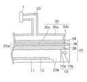
図1は第1実施形態例に係るプラズマ酸窒化装置の外観、図2は図1のA−A’を含む試料の処理面に垂直な方向における図1の装置の断面図、図3(a)は図1に示すプラズマ酸窒化装置のガス導入部の内部構造の分解斜視図、図3(b)は同図(a)のX−X’断面での断面図である。
[構成]
図1及び図2に示すように、第1実施形態例に係るプラズマ酸窒化装置は、マイクロ波発生器1、導波管2、同軸アンテナ3及びチャンバ4を有している。チャンバ4には、成膜ガス等のガスを導入するガス導入口5及びガスを排出するガス排出口6が取り付けられている。また、チャンバ4内部には、誘電体7、処理室8及びガス導入部10が設けられている。誘電体7の材質としては、石英、フッ素樹脂、ポリエチレン、ポリスチレン等の誘電損失の少ない物質が好ましい。
誘電体は、真空、空気、ガス等比誘電率が“1”である場合を含む。また、誘電体の表面の少なくとも一部が導体で覆われている場合を含む。
【0014】
処理室8には、試料12を載置するための試料台11が誘電体7と対向する位置に設けられている。処理室8の側面には、ガス導入口5から成膜ガス等のガスを処理室8に供給するガス導入部10が設けられている。ガス導入部10は、処理室8に開口を有するガス導入ノズル10a、及びガス導入口5と複数のガス導入ノズル10aとを連結するガス導入路10bを有している。なお、導波管2のかわりに、スロットアンテナ、矩形導波管、同軸アンテナ等その他のアンテナを設けても良い。
【0015】
以下に、ガス導入部10へのマイクロ波の進入を防止するためのマイクロ波遮断構造及び処理室8に概ね均一にガスを導入するためのガス導入構造について詳細に説明する(以下、“均一”とは“概ね均一”をいうものとする。)。まず、マイクロ波遮断構造について説明する。
[マイクロ波遮断構造]
ガスは、図3に示す矢印のように、ガス導入路10bからガス導入ノズル10aを通って処理室8へ供給される。このガス導入部10は、次の条件を満たすように構成されている。ガス導入ノズル10aは、処理室8からガス導入ノズル10aに導入されるマイクロ波の透過率Tが下記式(1)の関係を実質的に満たすように形成されている。
【0016】
【数5】
A1:ガス導入ノズル10aのガス進行方向と垂直な方向の長径、
λ:処理室8内のマイクロ波の波長である。
このように、ガス導入ノズル10aを設計することで、マイクロ波がガス導入部10へ進入するのを防止することができる。よって、ガス導入部10内において異常放電や膜の異常成長等が生じる問題を低減し、また均一なガス供給をすることができる。マイクロ波の損失を考慮して透過率Tが1%以下となるようにガス導入ノズル10aを設計すると好ましい。透過率が1%以下であると、マイクロ波の遮断効率が良く、異常放電や膜の異常成長等の問題をさらに防止できる。
[ガス導入構造]
次にガス導入構造について説明する。ガス導入路10bとガス導入ノズル10aとのガスの流れ易さ、所謂コンダクタンスの比を、X以上に設定すると良い。
ここで、Xは、ガス導入路10bに共通に接続されたガス導入ノズル10aの個数である。つまり、ガス導入路10bのコンダクタンスC2とガス導入ノズル10aのコンダクタンスC1との比は、以下の下記式(2)の関係を満たす。
【0017】
【数6】
【0018】
【数7】
【数8】
B1:ガス進行方向と垂直な方向のガス導入ノズル10aの短径、
L1:ガス進行方向のガス導入ノズル10aの長さ、
P1:ガス導入ノズル10a内の平均圧力、
K1:ガス導入ノズル10aの形状因子、
A2:ガス進行方向と垂直な方向のガス導入路10bの長径、
B2:ガス進行方向と垂直な方向のガス導入路10bの短径、
L2:ガス進行方向のガス導入路10bの長さ、
P2:ガス導入路10b内の平均圧力、
K2:ガス導入路10bの形状因子である。
【0020】
このように、ガス導入路10bとガス導入ノズル10aとのコンダクタンスの比を、ガス導入路10bに共通に接続されたガス導入ノズル10aの個数X以上にすることで、ガス導入ノズル10aから処理室8に均一にガスを供給することができる。よって、均一なガス供給により均一なプラズマを形成することができるので、均一な薄膜を形成することができる。なお、K1、K2は、ガス導入路10bの形状により“0”から“1”の値をとる。
ガス導入ノズル10aとガス導入路10bとのコンダクタンスの比を大きくすればすればするほど、均一にガスを供給することができるが、ガス導入部10の動作圧力、ガス流量、物理的耐性等を考慮して設定するのが好ましい。
【0021】
式(3)、式(4)の関係式は、上記の式に限定されるものではなく、流路の形状の違い等により適宜、適当な関係式を用いることができる。
[処理]
このプラズマ酸窒化装置では、例えば以下のように成膜の処理が行われる。
まず、ガス排出口6より排気を行って、処理室8内を所定の真空度にし、ガス導入口5、ガス導入路10b及びガス導入ノズル10aを介して処理室8内にガスを導入する。次に、マイクロ波発生器1より発生したマイクロ波を、導波管2を介して誘電体7に導入する。誘電体7は、導入されたマイクロ波を均一化し、処理室8内に導入する。導入されたマイクロ波により発生したプラズマは、ガス分子を励起・活性化させ化学種を生成し、試料12の表面に薄膜を形成する。
<第1実施例>
以下の図4〜図6を参照し、第1実施形態例に係るプラズマ酸窒化装置について、第1実施例を挙げてより具体的に説明する。図4は第1実施例のプラズマ酸窒化装置の外観、図5は図4のB−B’を含む図中X軸に垂直な図4の装置の断面図、図6は図4に示すプラズマ酸窒化装置の要部の分解斜視図である。
[全体構成]
本実施例に係るプラズマ酸窒化装置は、矩形導波管20、H面スロットアンテナ30及び試料12の処理面に沿う断面が矩形状のチャンバ(以下、矩形チャンバ)25を有している。前記第1実施形態例と同様に、マイクロ波発生器1、ガス導入口5、ガス排出口6及びガス導入部10が矩形チャンバ25に設けられている。また、矩形チャンバ25には、試料12の処理面に沿う断面が矩形状の処理室(以下、矩形処理室)25b及び矩形処理室25bを覆う、試料12の処理面に沿う断面が矩形状のチャンバ蓋(以下、矩形チャンバ蓋)25aが設けられている。
【0022】
矩形チャンバ蓋25aは、図6に示すように、上から順にそれぞれ、試料12の処理面に沿う断面が矩形状のアンテナ誘電体(以下、矩形アンテナ誘電体)34、スロット36aが設けられた、試料12の処理面に沿う断面が矩形状のスロット板(以下、矩形スロット板)36及び試料12の処理面に沿う断面が矩形状の封止誘電体(以下、矩形封止誘電体)38を有している。スロット板の材質としては、Cu、Al等の金属板が用いられる。矩形アンテナ誘電体34上には、H面スロットアンテナ30が載置されており、このH面スロットアンテナ30により矩形導波管20から矩形アンテナ誘電体34にマイクロ波が導入される。H面スロットアンテナ30は、上部30a、側部30b及び底部30cを有している。底部30cつまりH面スロットアンテナ30のH面には、図示しないスロットが形成されている。H面スロットアンテナ30上部には矩形導波管20が搭載されている。
【0023】
ここで、矩形アンテナ誘電体34は、その内部におけるマイクロ波の電界強度分布を、試料12の処理面に沿う方向に概ね均一化するための誘電体である(以下、電界強度分布が概ね均一なマイクロ波を、均一なマイクロ波と称する。また、以下の“均一”とは“試料12の処理面に沿う方向に概ね均一”をいうものとする)。
矩形アンテナ誘電体34下部の矩形スロット板36は、矩形アンテナ誘電体34から導入されるマイクロ波の電界強度分布の均一性を、スロット36aにより保持したままあるいはさらに高める。矩形スロット板36は、必ずしも試料12の処理面に沿う断面が矩形状である必要はなく、矩形アンテナ誘電体34、矩形封止誘電体38及び矩形処理室25bを覆う形状であれば良く、例えば、円形状であっても良い。
【0024】
矩形封止誘電体38は、矩形スロット板36より導入されたマイクロ波の電界強度分布の均一性を保持したままあるいはさらに高め、矩形封止誘電体38下方の矩形処理室25bにプラズマを発生させるための電界を形成する。また、矩形封止誘電体38は、真空状態の矩形処理室25bを大気から隔離し、清浄空間に保つ。
[ガス導入部の構成]
次に、ガス導入部10の構成を具体的に説明する。ガス導入部10は、矩形処理室25bに成膜ガス等のガスを供給するためにガス導入口5と接続され、ガス導入路10bとガス導入路10bに共通に設けられた80個のガス導入ノズル10aとを有している。ガス導入部10の分解斜視図は、図3と同様であり、ガス導入ノズル10aの形状は、A1=5mm,B1=1mm,L1=10mm、ガス導入路10bの形状は、A2=20mm,B2=20mm,L2=500mmに設定されている。このように設定すると、ガス導入ノズル10aにおけるマイクロ波の透過率Tは、前記式(1)より0.19%となる。また、1〜1000Torrまでの圧力域において、コンダクタンス比(C2/C1)は110以上となる。そのため、実施例1に係るプラズマ発生装置は、透過率Tが1%より十分に小さく、ガス導入部10へマイクロ波の進入をほぼ遮断して異常放電や膜の異常成長を低減している。また、コンダクタンス比が、ガス導入ノズル10aの個数80個よりも十分に大きいので、処理室8に均一にガスを供給することができる。よって、均一な薄膜を形成することができる。
【0025】
さらに、本実施例に係るプラズマ酸窒化装置は、試料12の処理面に沿う面方向にマイクロ波を伝搬させる領域、すなわち矩形アンテナ誘電体34及び矩形封止誘電体38が矩形状を有しているので、マイクロ波の電界強度分布が試料の処理面に沿って全体として均一となる。その均一なマイクロ波により均一にプラズマが発生し、このプラズマにより励起・活性化されたガス分子によって均一な薄膜形成が可能となる。また、ガスの流量・組成比等のプロセス条件の変更やメンテナンス等によるプロセス条件の変化が生じても、マイクロ波が伝播する領域が矩形状であるためマイクロ波の電界強度分布が偏りにくい。よって、プロセスマージンを拡大することができる。
【0026】
また、矩形アンテナ誘電体34により電界強度分布が均一化されたマイクロ波が、矩形スロット板36を介して均一に矩形封止誘電体38に導入され、矩形封止誘電体38によりさらに均一性が高められるので、マイクロ波の均一性を保持し易い。
[その他の実施形態例]
(A)本発明は、シリコンプロセス以外の化合物、FPD(Flat Panel Display)プロセス等に適用可能である。
(B)前記実施例は、必要に応じて組み合わせて用いることができる。
【0027】
【発明の効果】
本発明を用いれば、均一にガスを導入することができるプラズマ発生装置を提供することができる。
また、本発明を用いれば、異常放電や膜の異常成長の発生を防止することができるプラズマ発生装置を提供することができる。
【図面の簡単な説明】
【図1】第1実施形態例に係るプラズマ酸窒化装置の外観図。
【図2】図1のA−A’を含む試料の処理面に垂直な方向における図1の装置の断面図。
【図3】(a)図1に示すプラズマ酸窒化装置のガス導入部の内部構造の分解斜視図。
(b)(a)のX−X’断面での断面図。
【図4】第1実施例のプラズマ酸窒化装置の外観図。
【図5】図4のB−B’を含む図中X軸に垂直な図4の装置の断面図。
【図6】図4に示すプラズマ酸窒化装置の要部の分解斜視図。
【符号の説明】
1 マイクロ波発生器
2 導波管
3 同軸アンテナ
4 チャンバ
5 ガス導入口
6 ガス排出口
7 誘電体
8 処理室
10 ガス導入部
10a ガス導入ノズル
10b ガス導入路
12 試料
20 矩形導波管
25 矩形チャンバ
30 H面スロットアンテナ
34 矩形アンテナ誘電体
36 矩形スロット板
38 矩形封止誘電体[0001]
TECHNICAL FIELD OF THE INVENTION
The present invention relates to a plasma generator using plasma generated by microwaves.
[0002]
[Prior art]
A plasma generator using a microwave (for example, 2.45 GHz) is used for forming an integrated circuit (IC). In the plasma generator using microwaves, high-density and low-electron-temperature plasma can be obtained by microwaves having a high frequency. Therefore, it is possible to suppress the influence of electrical or physical damage to a thin film such as a gate oxide film.
[0003]
[Problems to be solved by the invention]
However, in response to recent demands for finer ICs and larger wafer diameters, conventional gas supply systems provide uniform processing of samples when performing processes such as film formation, etching, ashing, sputtering, and cleaning. The problem that processing is difficult is occurring. For example, when performing processing such as film formation, a processing gas is introduced into a processing chamber from a gas introduction unit. At this time, microwaves enter the gas introduction unit from the processing chamber, causing a problem that abnormal discharge or abnormal film growth occurs in the gas introduction unit.
Further, since an opening is provided in the processing chamber to form a gas introduction portion, the supply of non-uniform gas causes non-uniform microwaves in the processing chamber and non-uniform plasma. Therefore, it is difficult to uniformly process the sample by the non-uniform plasma.
[0004]
Therefore, an object of the present invention is to provide a plasma generator capable of uniformly introducing a gas.
Another object of the present invention is to provide a plasma generator capable of preventing occurrence of abnormal discharge and abnormal growth of a film.
[0005]
[Means for Solving the Problems]
In order to solve the above-mentioned problems, a first invention of the present application is directed to a microwave generator, a reactor connected to the microwave generator, and generating plasma by microwaves generated from the microwave generator, Provided is a plasma generator having an introduction path for supplying a gas to a reactor, and at least one nozzle connecting the reactor and the introduction path. In this plasma generator, the microwave transmission T from the reactor to the nozzle substantially satisfies the following equation (1).
[0006]
[Equation 3]
By designing the nozzle so that the microwave transmittance T satisfies the expression (1), it is possible to reduce the entry of the microwave into the introduction portion. Therefore, it is possible to reduce a problem that abnormal discharge or abnormal film growth occurs in the introduction portion, and to supply a substantially uniform gas (hereinafter, “uniform” means “substantially uniform”). .
[0007]
The present second invention is the first invention, the ratio of the conductance C 2 of the gas of the conductance C 1 and the introduction path of the gas within the nozzle, to provide a plasma generating apparatus which satisfies the following formula (2) .
[0008]
(Equation 4)
By setting the ratio of the conductance of the gas between the introduction path and the nozzle to be equal to or more than the number of nozzles connected to the introduction path, gas can be supplied to the reactor from the introduction path to the reactor substantially uniformly through the nozzles.
The third invention of the present application provides the plasma generator according to the second invention, wherein the transmittance T is 1% or less.
[0009]
By employing a microwave blocking structure in which the transmittance T of microwaves introduced from the reactor via a nozzle is 1% or less, abnormal discharge and abnormal growth of a film can be further reduced.
According to a fourth aspect of the present invention, in the first aspect, the electric field intensity distribution of the microwave generated from the microwave generating means, which is connected to the microwave generating means and has a rectangular cross section along a processing surface of the sample, is provided. A plasma generator comprising a first dielectric, which is made substantially uniform along a processing surface of a sample to be subjected to plasma processing in the reactor, and processing means for processing the sample using the plasma.
[0010]
Since the first dielectric has a rectangular shape, the electric field intensity distribution of the microwave becomes uniform as a whole along the processing surface of the sample. Therefore, uniform plasma is generated by the uniform microwave, and a uniform thin film can be formed by gas molecules excited and activated by the plasma. Further, even if the process conditions such as the flow rate and the composition ratio of the gas are changed or the process conditions are changed due to maintenance or the like, the microwave electric field intensity distribution is not easily biased because the region where the microwave propagates is rectangular. Therefore, the process margin can be expanded.
[0011]
According to a fifth aspect of the present invention, in the fourth aspect, at least one slot is formed below the first dielectric, and the uniformity of the microwave electric field intensity distribution in the first dielectric is maintained. Alternatively, a slot plate is provided between the slot plate and the reactor, and the uniformity of the electric field intensity distribution of the microwave supplied from the slot plate is maintained or further increased. A plasma generator having a second dielectric having a rectangular cross section is provided.
Since the second dielectric has a rectangular shape, plasma can be generated more uniformly. In addition, since uniformity is enhanced by the first dielectric, the slot plate, and the second dielectric, uniformity of microwaves can be easily maintained.
[0012]
BEST MODE FOR CARRYING OUT THE INVENTION
<Plasma processing equipment>
The plasma processing apparatus has a microwave generator, a processing chamber, and a microwave propagation region above the processing chamber, and performs processing as described below.
Microwaves generated by the microwave generator propagate in the microwave propagation region, and an electric field is formed in the processing chamber in a gas atmosphere. Plasma is generated by the electric field and the gas, and processing such as film formation, etching, and gas-phase cleaning is performed on a sample in the processing chamber by the chemical species generated by the plasma.
[0013]
Examples of such a plasma processing apparatus using plasma include an apparatus that performs oxidation and nitridation using plasma (hereinafter, referred to as a plasma oxynitridation apparatus), a plasma CVD (Chemical Vapor Deposition) apparatus, a plasma etching apparatus, a plasma ashing apparatus, and a plasma cleaning apparatus. Equipment, plasma annealing equipment and the like.
Hereinafter, the plasma generating apparatus of the present invention will be described using a plasma oxynitriding apparatus as an example.
<First Embodiment>
1 is an external view of a plasma oxynitriding apparatus according to the first embodiment, FIG. 2 is a cross-sectional view of the apparatus of FIG. 1 in a direction perpendicular to a processing surface of a sample including AA ′ in FIG. 1, and FIG. 3) is an exploded perspective view of the internal structure of the gas introduction part of the plasma oxynitriding apparatus shown in FIG. 1, and FIG.
[Constitution]
As shown in FIGS. 1 and 2, the plasma oxynitriding apparatus according to the first embodiment has a
The dielectric includes a case where the relative dielectric constants of vacuum, air, and gas are “1”. Also, a case where at least a part of the surface of the dielectric is covered with a conductor is included.
[0014]
In the
[0015]
Hereinafter, a microwave blocking structure for preventing microwaves from entering the
[Microwave blocking structure]
The gas is supplied from the
[0016]
(Equation 5)
A 1 : the major axis in the direction perpendicular to the gas traveling direction of the
λ: wavelength of the microwave in the
By designing the
[Gas introduction structure]
Next, the gas introduction structure will be described. It is preferable that the ease of gas flow between the
Here, X is the number of
[0017]
(Equation 6)
[0018]
(Equation 7)
(Equation 8)
B 1 : short diameter of the
L 1 : length of the
P 1 : average pressure in the
K 1 : form factor of
A 2 : the major axis of the
B 2 : short diameter of the
L 2 : length of the
P 2 : average pressure in the
K 2 : a form factor of the
[0020]
As described above, by setting the ratio of the conductance between the
The larger the ratio of the conductance between the
[0021]
The relational expressions of Expressions (3) and (4) are not limited to the above expressions, and an appropriate relational expression can be used as appropriate depending on a difference in the shape of the flow path and the like.
[processing]
In this plasma oxynitriding apparatus, for example, a film forming process is performed as follows.
First, the interior of the
<First embodiment>
The plasma oxynitriding apparatus according to the first embodiment will be described more specifically with reference to FIGS. FIG. 4 is an external view of the plasma oxynitriding apparatus of the first embodiment, FIG. 5 is a cross-sectional view of the apparatus of FIG. 4 including BB ′ of FIG. 4 and is perpendicular to the X axis in FIG. 4, and FIG. FIG. 2 is an exploded perspective view of a main part of the oxynitriding device.
[overall structure]
The plasma oxynitriding apparatus according to the present embodiment includes a
[0022]
As shown in FIG. 6, the
[0023]
Here, the
The
[0024]
The
[Configuration of gas introduction unit]
Next, the configuration of the
[0025]
Furthermore, in the plasma oxynitriding apparatus according to the present embodiment, the region where microwaves are propagated in the surface direction along the processing surface of the
[0026]
The microwave whose electric field intensity distribution is made uniform by the
[Other Embodiment Examples]
(A) The present invention is applicable to compounds other than the silicon process, FPD (Flat Panel Display) processes, and the like.
(B) The above embodiments can be used in combination as needed.
[0027]
【The invention's effect】
According to the present invention, a plasma generator capable of uniformly introducing a gas can be provided.
Further, according to the present invention, it is possible to provide a plasma generator capable of preventing occurrence of abnormal discharge and abnormal growth of a film.
[Brief description of the drawings]
FIG. 1 is an external view of a plasma oxynitriding apparatus according to a first embodiment.
FIG. 2 is a cross-sectional view of the apparatus of FIG. 1 in a direction perpendicular to a processing surface of a sample including AA ′ of FIG. 1;
FIG. 3A is an exploded perspective view of an internal structure of a gas introduction unit of the plasma oxynitriding apparatus shown in FIG.
(B) Sectional drawing in the XX 'cross section of (a).
FIG. 4 is an external view of a plasma oxynitriding apparatus according to the first embodiment.
FIG. 5 is a cross-sectional view of the device of FIG. 4 perpendicular to the X-axis in the drawing including BB ′ of FIG. 4;
6 is an exploded perspective view of a main part of the plasma oxynitriding apparatus shown in FIG.
[Explanation of symbols]
DESCRIPTION OF
Claims (5)
前記マイクロ波発生手段に接続され、前記マイクロ波発生手段から発生したマイクロ波によりプラズマが発生する反応器と、
前記反応器にガスを供給するための導入路と、
前記反応器と前記導入路とを連結する少なくとも一つのノズルとを有し、
前記反応器から前記ノズルへのマイクロ波の透過率Tは、実質的に、下記式(1)を満たすプラズマ発生装置
A1:前記ノズルのガス進行方向と垂直な方向の長径
λ:前記反応器内のマイクロ波の波長。Microwave generating means;
A reactor connected to the microwave generation means, wherein a plasma is generated by microwaves generated from the microwave generation means,
An introduction path for supplying gas to the reactor,
Having at least one nozzle connecting the reactor and the introduction path,
A plasma generation apparatus in which the microwave transmittance T from the reactor to the nozzle substantially satisfies the following expression (1)
前記プラズマを用いて前記試料を処理する処理手段と、を有する請求項1に記載のプラズマ発生装置。Connected to the microwave generation means, the cross section along the processing surface of the sample is rectangular, the distribution of the electric field intensity of the microwave generated from the microwave generation means, the sample subjected to plasma processing in the reactor A first dielectric that is substantially uniform along the processing surface;
The plasma generator according to claim 1, further comprising: a processing unit configured to process the sample using the plasma.
前記スロット板と前記反応器との間に設けられ、前記スロット板から供給されるマイクロ波の電界強度分布の均一性を保持またはさらに高める、前記試料の処理面に沿う断面が矩形状の第2誘電体と、をさらに有する請求項4に記載のプラズマ発生装置。A slot plate provided below the first dielectric and having at least one slot formed therein, for maintaining or further improving the uniformity of the electric field intensity distribution of microwaves in the first dielectric;
A second section, which is provided between the slot plate and the reactor and has a rectangular cross section along the processing surface of the sample, which maintains or further enhances the uniformity of the electric field intensity distribution of the microwave supplied from the slot plate. The plasma generator according to claim 4, further comprising: a dielectric.
Priority Applications (2)
| Application Number | Priority Date | Filing Date | Title |
|---|---|---|---|
| JP2003022072A JP3934559B2 (en) | 2003-01-30 | 2003-01-30 | Plasma generator |
| US10/707,989 US6998565B2 (en) | 2003-01-30 | 2004-01-30 | Plasma processing apparatus |
Applications Claiming Priority (1)
| Application Number | Priority Date | Filing Date | Title |
|---|---|---|---|
| JP2003022072A JP3934559B2 (en) | 2003-01-30 | 2003-01-30 | Plasma generator |
Publications (2)
| Publication Number | Publication Date |
|---|---|
| JP2004235430A true JP2004235430A (en) | 2004-08-19 |
| JP3934559B2 JP3934559B2 (en) | 2007-06-20 |
Family
ID=32951241
Family Applications (1)
| Application Number | Title | Priority Date | Filing Date |
|---|---|---|---|
| JP2003022072A Expired - Fee Related JP3934559B2 (en) | 2003-01-30 | 2003-01-30 | Plasma generator |
Country Status (1)
| Country | Link |
|---|---|
| JP (1) | JP3934559B2 (en) |
-
2003
- 2003-01-30 JP JP2003022072A patent/JP3934559B2/en not_active Expired - Fee Related
Also Published As
| Publication number | Publication date |
|---|---|
| JP3934559B2 (en) | 2007-06-20 |
Similar Documents
| Publication | Publication Date | Title |
|---|---|---|
| US5575883A (en) | Apparatus and process for fabricating semiconductor devices | |
| JP4273932B2 (en) | Surface wave excitation plasma CVD equipment | |
| KR100960424B1 (en) | Microwave plasma processing device | |
| US6263830B1 (en) | Microwave choke for remote plasma generator | |
| US7728251B2 (en) | Plasma processing apparatus with dielectric plates and fixing member wavelength dependent spacing | |
| TWI461114B (en) | Stable surface wave plasma source | |
| US20080134974A1 (en) | Plasma processing apparatus and gas through plate | |
| JP5520455B2 (en) | Plasma processing equipment | |
| US7897009B2 (en) | Plasma processing apparatus | |
| JP2007048718A (en) | Plasma treatment device | |
| US20080105650A1 (en) | Plasma processing device and plasma processing method | |
| US20130012033A1 (en) | Silicon oxide film forming method and plasma oxidation apparatus | |
| EP1895565A1 (en) | Plasma processing apparatus and method | |
| JP2003203869A (en) | Plasma treatment device | |
| US7779783B2 (en) | Plasma processing device | |
| JP2003142471A (en) | Plasma treatment apparatus and method of manufacturing constitutional body | |
| JP3934559B2 (en) | Plasma generator | |
| JPH0729889A (en) | Microwave plasma treatment processing equipment | |
| JP2023016557A (en) | Plasma source and plasma processing apparatus | |
| JP2001326216A (en) | Plasma processing device | |
| JPH04211118A (en) | Microwave plasma processing apparatus | |
| JP2003332241A (en) | Microwave plasma treatment apparatus, microwave plasma treatment method, and structure manufacturing method | |
| JP3934560B2 (en) | Plasma processing equipment | |
| JP3364131B2 (en) | Plasma processing equipment | |
| JP2011029250A (en) | Microwave plasma processing apparatus, and microwave plasma processing method |
Legal Events
| Date | Code | Title | Description |
|---|---|---|---|
| A977 | Report on retrieval |
Free format text: JAPANESE INTERMEDIATE CODE: A971007 Effective date: 20041209 |
|
| A131 | Notification of reasons for refusal |
Free format text: JAPANESE INTERMEDIATE CODE: A131 Effective date: 20041221 |
|
| A521 | Written amendment |
Free format text: JAPANESE INTERMEDIATE CODE: A523 Effective date: 20050218 |
|
| A131 | Notification of reasons for refusal |
Free format text: JAPANESE INTERMEDIATE CODE: A131 Effective date: 20070116 |
|
| A521 | Written amendment |
Free format text: JAPANESE INTERMEDIATE CODE: A523 Effective date: 20070220 |
|
| TRDD | Decision of grant or rejection written | ||
| A01 | Written decision to grant a patent or to grant a registration (utility model) |
Free format text: JAPANESE INTERMEDIATE CODE: A01 Effective date: 20070313 |
|
| A61 | First payment of annual fees (during grant procedure) |
Free format text: JAPANESE INTERMEDIATE CODE: A61 Effective date: 20070315 |
|
| R150 | Certificate of patent (=grant) or registration of utility model |
Free format text: JAPANESE INTERMEDIATE CODE: R150 |
|
| LAPS | Cancellation because of no payment of annual fees |