JP2004233844A - Device and method for display, and apparatus and method for image processing - Google Patents
Device and method for display, and apparatus and method for image processing Download PDFInfo
- Publication number
- JP2004233844A JP2004233844A JP2003024420A JP2003024420A JP2004233844A JP 2004233844 A JP2004233844 A JP 2004233844A JP 2003024420 A JP2003024420 A JP 2003024420A JP 2003024420 A JP2003024420 A JP 2003024420A JP 2004233844 A JP2004233844 A JP 2004233844A
- Authority
- JP
- Japan
- Prior art keywords
- image
- display
- image signal
- correction data
- switching
- Prior art date
- Legal status (The legal status is an assumption and is not a legal conclusion. Google has not performed a legal analysis and makes no representation as to the accuracy of the status listed.)
- Pending
Links
Images


Abstract
Description
【0001】
【発明の属する技術分野】
この発明は、画像信号を表示する表示装置及び表示方法に係り、特に大画面のフラットパネルディスプレイに使用して好適するものに関する。また、この発明は、上記した表示装置及び表示方法に画像信号を与える画像処理装置及び画像処理方法に関する。
【0002】
【従来の技術】
周知のように、近年では、薄型で大画面表示が可能であることから、CRT(Cathode Ray Tube)に代えてフラットパネルディスプレイの開発が盛んに行なわれている。
【0003】
このフラットパネルディスプレイとして、現状では、例えば、液晶ディスプレイ、プラズマディスプレイ、EL(Electro Luminescence)ディスプレイ、FED(Field Emission Display)等が開発されている。
【0004】
ところで、このようなフラットパネルディスプレイにおいては、その表示画素毎の性能のばらつきを補正するために、全ての表示画素に対してそれぞれ補正データを用意する必要がある。
【0005】
この補正データは、通常、制御用のマイクロコンピュータから各表示画素を駆動するためのドライバにシリアルで転送され、ドライバ内の補正テーブルに格納されることにより、各表示画素の補正に供される。
【0006】
この場合、マイクロコンピュータからドライバに補正データをシリアルで転送しているのは、ドライバに接続される伝送ライン数を減らして、IC(Integrated Circuit)化した際にピン数の占有を極力削減するためである。
【0007】
ところが、フラットパネルディスプレイを構成する全ての表示画素は、それぞれが、R(Red)、G(Green)、B(Blue)成分の表示を行なう3つの画素から構成されている。そして、補正データは、全ての画素に対して用意される必要があることから、全表示画素数の3倍のデータ量となる。
【0008】
このため、現状のフラットパネルディスプレイでは、このような膨大な量の補正データをドライバにシリアルで転送していることから、転送に要する時間が長くなるという問題が生じている。
【0009】
ここで、特許文献1には、映像データの階調に対する輝度特性を検出し、この検出された輝度特性に応じて階調を補正し、この補正された階調を液晶パネルに表示させる構成が開示されている。
【0010】
また、特許文献2には、複数の画像伝送線の信号を時分割により1本のデータ伝送線の信号とすることで、データ伝送線数を画像伝送線数より少なくして表示装置の配線数を減らす構成が開示されている。
【0011】
しかしながら、これらの特許文献1,2には、いずれも、画像信号とは別に多量の補正データを、ピン数を増やすことなく短時間で転送可能となすように対処することについては、何らの記載もなされていないものである。
【0012】
【特許文献1】
特開2001−343957号公報
【0013】
【特許文献2】
特開2001−255841号公報
【0014】
【発明が解決しようとする課題】
そこで、この発明は上記事情を考慮してなされたもので、画像信号とは別個に存在する多量の補正データを、伝送ライン数を増加することなく短時間で転送可能とした表示装置及び表示方法、画像処理装置及び画像処理方法を提供することを目的とする。
【0015】
【課題を解決するための手段】
この発明に係る表示装置は、複数の表示画素を有する画像表示手段と、この画像表示手段に画像表示させるための画像信号と画像表示手段の各表示画素に対する補正データとを選択的に切り替えて出力する切替手段と、この切替手段から出力される画像信号に基づいて画像表示手段に画像表示を行なわせるとともに切替手段から出力される補正データに基づいて画像表示手段の各表示画素を補正する制御手段とを備えるようにしたものである。
【0016】
また、この発明に係る表示方法は、複数の表示画素を有する画像表示手段に画像表示を行なわせるための画像信号と画像表示手段の各表示画素に対する補正データとを選択的に切り替える工程と、選択された画像信号に基づいて画像表示手段に画像表示を行なわせる工程と、選択された補正データに基づいて画像表示手段の各表示画素を補正する工程とを有するようにしたものである。
【0017】
さらに、この発明に係る表示装置は、複数の表示画素を有する画像表示手段と、この画像表示手段に画像表示させるための画像信号と画像表示手段の各表示画素に対する補正データとが同一ラインを介して選択的に入力され、画像信号に基づいて画像表示手段に画像表示を行なわせるとともに補正データに基づいて画像表示手段の各表示画素を補正する制御手段とを備えるようにしたものである。
【0018】
また、この発明に係る表示方法は、複数の表示画素を有する画像表示手段に画像表示を行なわせるための画像信号と画像表示手段の各表示画素に対する補正データとを同一ラインを介して選択的に入力する工程と、入力された画像信号に基づいて画像表示手段に画像表示を行なわせる工程と、入力された補正データに基づいて画像表示手段の各表示画素を補正する工程とを有するようにしたものである。
【0019】
さらに、この発明に係る画像処理装置は、画像信号を出力する画像出力手段と、補正データを出力する補正出力手段と、画像出力手段から出力される画像信号と補正出力手段から出力される補正データとを同一ラインを介して選択的に切り替えて出力する出力手段とを備えるようにしたものである。
【0020】
また、この発明に係る画像処理方法は、画像信号を出力する工程と、補正データを出力する工程と、画像信号の有効期間に画像信号、画像信号の非有効期間に補正データを、同一ラインを介して選択的に切り替えて出力する工程とを有するようにしたものである。
【0021】
上記のような構成及び方法によれば、補正データを画像信号の伝送ラインを利用して転送するようにしたので、画像信号とは別個に存在する多量の補正データを、伝送ライン数を増加させることなく短時間で転送することが可能となる。
【0022】
【発明の実施の形態】
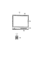
以下、この発明の第1の実施の形態について図面を参照して詳細に説明する。図1は、この第1の実施の形態で説明するテレビジョン受信装置11の外観を示している。
【0023】
このテレビジョン受信装置11は、略箱状に形成された筐体12の前面部13に、複数の表示画素をマトリクス状に配置したフラットパネルディスプレイ14と、電源スイッチや各種のキーで構成された操作部15とを配置している。
【0024】
また、このテレビジョン受信装置11は、操作部15の操作情報を受けるだけでなく、ワイヤレスのリモートコントローラ16からの操作情報も受けて、その動作を制御している。
【0025】
図2は、このテレビジョン受信装置11の信号処理系の詳細を示している。まず、図2において、符号17は、テレビジョン放送電波を受信するアンテナである。
【0026】
このアンテナ17に誘起されたテレビジョン信号は、チューナ部18に供給される。このチューナ部18は、入力されたテレビジョン信号から所望の放送チャンネルの画像信号を選局し、パラレルに出力している。
【0027】
このチューナ部18からパラレル出力された画像信号は、画像処理部19に供給されて所定の復調処理が施された後、切替部20を通過してドライバ21に供給される。
【0028】
このドライバ21は、入力された画像信号に基づいて、フラットパネルディスプレイ14の各表示画素をそれぞれ制御して、フラットパネルディスプレイ14に画像表示を行なわせるように制御している。
【0029】
上記したテレビジョン信号の一連の再生動作は、マイクロコンピュータ22によって統括的に制御されている。このマイクロコンピュータ22は、上記操作部15から得られる操作情報、または、上記リモートコントローラ16から受信部23を介して得られる操作情報を受けて、ユーザの要求する動作状態が実現されるように、各部18〜21を制御している。
【0030】
この場合、マイクロコンピュータ22は、記憶部24に格納された制御プログラムや各種の設定値等に基づいて、また、記憶部24をワークエリアとして、各部18〜21の制御を行なっている。
【0031】
ここで、上記マイクロコンピュータ22は、フラットパネルディスプレイ14を構成する全ての画素に対する補正データを生成して、切替部20にパラレルに出力している。この切替部20は、通常、画像処理部19からパラレル出力される画像信号を、ドライバ21に導くように切り替えられている。
【0032】
一方、この切替部21は、マイクロコンピュータ22がフラットパネルディスプレイ14の各画素に対する補正要求を発生した場合、該補正要求に基づいて画像処理部19から発生される切替信号により、マイクロコンピュータ22からパラレル出力される補正データをドライバ21に導くように切り替えられる。
【0033】
この場合、切替部20は、マイクロコンピュータ22からパラレル出力される補正データが、画像処理部19からパラレル出力される画像信号の有効期間以外の期間でドライバ21に転送されるように、切り替え制御されている。
【0034】
そして、マイクロコンピュータ22からパラレル出力された補正データは、ドライバ21に内蔵されたメモリ21aに補正テーブルとして格納されることにより、フラットパネルディスプレイ14の各画素の補正に供される。
【0035】
上記した実施の形態によれば、画像処理部19からパラレル出力される画像信号をドライバ21に伝送するために元々存在するバスラインBLを利用して、画像信号の非有効期間にマイクロコンピュータ22から出力される補正データをパラレルでドライバ21に入力させている。
【0036】
このため、ドライバ21に接続される伝送ライン数を増加させることなく、多量の補正データをパラレルにより短時間でドライバ21に転送することが可能となる。
【0037】
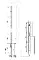
図3は、画像信号と切替信号との関係を示している。図3では、ANSI(American National Standards Institute)/SMPTE 296M−1997に規定されている、有効水平画素数1280×有効垂直ライン数720の画像信号を例にとり、その1ライン分を示している。
【0038】
すなわち、この1ラインの画像信号は、水平画素同期クロックの1周期を1Tとすると、4TのEAV期間、362Tの水平ブランキング期間及び4TのSAV期間とでなる370Tの非有効期間と、実質的な画像成分でなる1280Tの有効期間とから構成されている。
【0039】
このため、上記画像処理部19は、復調して得られた1ラインの画像信号の有効期間に、切替部20に対して、画像処理部19からパラレル出力される画像信号をドライバ21に導くように切り替えるためのH(High)レベルの切替信号を発生する。
【0040】
また、上記画像処理部19は、復調して得られた1ラインの画像信号の非有効期間に、切替部20に対して、マイクロコンピュータ22からパラレル出力される補正データをドライバ21に導くように切り替えるためのL(Low)レベルの切替信号を発生する。
【0041】
図4は、図3に示した切替信号を生成するために、画像処理部19の内部に設置された切替信号生成部の詳細を示している。この切替信号生成部は、カウンタ19aとデコーダ19bとから構成されている。
【0042】
このうち、カウンタ19aは、マイクロコンピュータ22から出力される補正要求信号に基づいて駆動されるもので、駆動後は、水平画素同期クロックをカウントし、水平同期信号によって水平周期でリセットされるという動作を繰り返している。
【0043】
そして、上記デコーダ19bは、カウンタ19aのカウント値に基づいて、1ラインの画像信号の非有効期間と有効期間とを判別することにより切替信号を生成し、切替部20に出力している。
【0044】
図5は、画像信号と切替信号との関係の他の例を示している。すなわち、上記した有効水平画素数1280×有効垂直ライン数720の画像信号は、その全垂直ライン数として750を有している。
【0045】
そして、ライン番号1〜25までの25ラインと、ライン番号746〜750までの5ラインとの30本のラインが、画像成分の含まれない非有効ラインとなっている。
【0046】
このため、画像成分を含む、ライン番号26〜745までの720本の有効ライン期間に、切替部20に対して、画像処理部19からパラレル出力される画像信号をドライバ21に導くように切り替えるためのH(High)レベルの切替信号を発生する。
【0047】
また、画像成分を含まない、ライン番号1〜25までとライン番号746〜750までの非有効ライン期間に、切替部20に対して、マイクロコンピュータ22からパラレル出力される補正データをドライバ21に導くように切り替えるためのL(Low)レベルの切替信号を発生する。
【0048】
図6は、画像信号と切替信号との関係のさらに他の例を示している。これは、図3に示した関係と図5に示した関係とを両方組み合わせたものである。すなわち、画像成分を含む、ライン番号26〜745までの720本の有効ライン期間においては、1ラインの画像信号の非有効期間と有効期間とで切替信号をLレベルとHレベルとに切り替える。また、画像成分を含まない、ライン番号1〜25までとライン番号746〜750までの非有効ライン期間においては、切替信号をLレベルに切り替えている。
【0049】
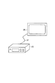
図7は、この発明の第2の実施の形態を示している。この第2の実施の形態では、テレビジョン放送を受信して画像信号の選局及び復調を行なう受信装置25と、この受信装置25で復調された画像信号を表示する表示装置26とが別体であり、両者がケーブル27で接続される構成となっている。
【0050】
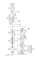
図8は、この受信装置25及び表示装置26の詳細を示している。なお、図8において、図2と同一部分には同一符号を付して示している。この場合、受信装置25が、アンテナ17、チューナ部18、画像処理部19、切替部20、受信部23、操作部15、マイクロコンピュータ22、記憶部24及びリモートコントローラ16を備える構成となる。また、表示装置26が、ドライバ21とフラットパネルディスプレイ14とを備える構成となる。
【0051】
そして、切替部20からドライバ21に画像信号または補正データをパラレルで転送するためのバスライン27aと、マイクロコンピュータ22からドライバ21に制御情報を転送するための制御ライン27bとが、ケーブル27としてまとめられている。
【0052】
このように、受信装置25及び表示装置26を別体に構成しても、ドライバ21に接続される伝送ライン数を増加させることなく、多量の補正データをパラレルにより短時間でドライバ21に転送することが可能となり、第1の実施の形態と同様な効果を得ることができる。
【0053】
また、上記した第1及び第2の実施の形態では、いずれも、テレビジョン放送を受信して表示する装置について述べたが、この発明は、これに限らず、例えば記録媒体から画像信号を再生して表示する装置等にも、広く適用することが可能である。
【0054】
ここで、フラットパネルディスプレイ14の各画素に対して補正データによる補正処理を施すタイミングは、メーカによる製造時の調整段階、ユーザの要求、新規な補正データがダウンロードされた場合、経年変化による再調整時等が考えられる。
【0055】
なお、この発明は上記した各実施の形態に限定されるものではなく、この外その要旨を逸脱しない範囲で種々変形して実施することができる。
【0056】
【発明の効果】
以上詳述したようにこの発明によれば、画像データとは別個に存在する多量の補正データを、伝送ライン数を増加することなく短時間で転送可能とした表示装置及び表示方法、画像処理装置及び画像処理方法を提供することができる。
【図面の簡単な説明】
【図1】この発明の第1の実施の形態を示すもので、テレビジョン受信装置を説明するために示す外観図。
【図2】同第1の実施の形態におけるテレビジョン受信装置の信号処理系の詳細を説明するために示すブロック構成図。
【図3】同第1の実施の形態におけるテレビジョン受信装置の画像信号と切替信号との関係の一例を説明するために示す図。
【図4】同第1の実施の形態におけるテレビジョン受信装置の切替信号生成部の詳細を説明するために示すブロック構成図。
【図5】同第1の実施の形態におけるテレビジョン受信装置の画像信号と切替信号との関係の他の例を説明するために示す図。
【図6】同第1の実施の形態におけるテレビジョン受信装置の画像信号と切替信号との関係のさらに他の例を説明するために示す図。
【図7】この発明の第2の実施の形態を示すもので、受信装置と表示装置とを説明するために示す外観図。
【図8】同第2の実施の形態における受信装置及び表示装置の信号処理系の詳細を説明するために示すブロック構成図。
【符号の説明】
11…テレビジョン受信装置、12…筐体、13…前面部、14…フラットパネルディスプレイ、15…操作部、16…リモートコントローラ、17…アンテナ、18…チューナ部、19…画像処理部、20…切替部、21…ドライバ、22…マイクロコンピュータ、23…受信部、24…記憶部、25…受信装置、26…表示装置、27…ケーブル。[0001]
TECHNICAL FIELD OF THE INVENTION
The present invention relates to a display device and a display method for displaying an image signal, and more particularly to a display device suitable for use in a large-screen flat panel display. The present invention also relates to an image processing device and an image processing method for providing an image signal to the above-described display device and display method.
[0002]
[Prior art]
As is well known, in recent years, flat panel displays have been actively developed in place of CRTs (Cathode Ray Tubes) because they are thin and capable of displaying large screens.
[0003]
At present, for example, a liquid crystal display, a plasma display, an EL (Electro Luminescence) display, a FED (Field Emission Display), and the like have been developed as the flat panel display.
[0004]
By the way, in such a flat panel display, it is necessary to prepare correction data for all the display pixels in order to correct the variation in the performance for each display pixel.
[0005]
This correction data is usually transferred serially from a control microcomputer to a driver for driving each display pixel, and stored in a correction table in the driver, so as to be used for correction of each display pixel.
[0006]
In this case, the reason why the correction data is serially transferred from the microcomputer to the driver is to reduce the number of transmission lines connected to the driver and to reduce the occupation of the number of pins as much as possible when an integrated circuit (IC) is used. It is.
[0007]
However, all the display pixels constituting the flat panel display are each composed of three pixels for displaying R (Red), G (Green), and B (Blue) components. Since the correction data needs to be prepared for all the pixels, the data amount is three times the total number of display pixels.
[0008]
For this reason, in the current flat panel display, since such an enormous amount of correction data is serially transferred to the driver, there is a problem that the time required for the transfer becomes long.
[0009]
Here, Patent Document 1 discloses a configuration in which a luminance characteristic with respect to a gradation of video data is detected, the gradation is corrected according to the detected luminance characteristic, and the corrected gradation is displayed on a liquid crystal panel. It has been disclosed.
[0010]
Further, Patent Document 2 discloses that the number of data transmission lines is made smaller than the number of image transmission lines by making the signals of a plurality of image transmission lines into one data transmission line signal in a time-division manner. Are disclosed.
[0011]
However, these Patent Documents 1 and 2 do not disclose any technique for transferring a large amount of correction data separately from image signals in a short time without increasing the number of pins. It has not been done.
[0012]
[Patent Document 1]
JP 2001-343957 A
[Patent Document 2]
JP 2001-255841 A
[Problems to be solved by the invention]
Therefore, the present invention has been made in consideration of the above circumstances, and a display device and a display method capable of transferring a large amount of correction data existing separately from an image signal in a short time without increasing the number of transmission lines. It is an object to provide an image processing apparatus and an image processing method.
[0015]
[Means for Solving the Problems]
A display device according to the present invention outputs image display means having a plurality of display pixels, and selectively switches between an image signal for displaying an image on the image display means and correction data for each display pixel of the image display means. Switching means for performing the image display on the image display means based on the image signal output from the switching means, and correcting each display pixel of the image display means based on the correction data output from the switching means. And so on.
[0016]
The display method according to the present invention further includes a step of selectively switching between an image signal for causing an image display means having a plurality of display pixels to perform image display and correction data for each display pixel of the image display means. And a step of correcting each display pixel of the image display means on the basis of the selected correction data.
[0017]
Further, in the display device according to the present invention, the image display means having a plurality of display pixels, an image signal for causing the image display means to display an image, and correction data for each display pixel of the image display means are transmitted via the same line. Control means for selectively inputting and displaying an image on the image display means based on the image signal, and correcting each display pixel of the image display means based on the correction data.
[0018]
Also, the display method according to the present invention selectively outputs, via the same line, an image signal for causing an image display means having a plurality of display pixels to perform image display and correction data for each display pixel of the image display means. An input step; a step of causing the image display means to perform image display based on the input image signal; and a step of correcting each display pixel of the image display means based on the input correction data. Things.
[0019]
Further, the image processing apparatus according to the present invention includes an image output unit that outputs an image signal, a correction output unit that outputs correction data, an image signal output from the image output unit, and correction data output from the correction output unit. And an output unit for selectively switching and outputting via the same line.
[0020]
Also, the image processing method according to the present invention includes a step of outputting an image signal, a step of outputting correction data, and a step of outputting an image signal during a valid period of the image signal, correction data during a non-valid period of the image signal, and And selectively switching and outputting the data through the interface.
[0021]
According to the above configuration and method, the correction data is transferred using the transmission line of the image signal, so that a large amount of correction data existing separately from the image signal is increased in the number of transmission lines. It is possible to transfer in a short time without any problem.
[0022]
BEST MODE FOR CARRYING OUT THE INVENTION
Hereinafter, a first embodiment of the present invention will be described in detail with reference to the drawings. FIG. 1 shows an appearance of a
[0023]
The
[0024]
Further, the
[0025]
FIG. 2 shows details of a signal processing system of the
[0026]
The television signal induced by the
[0027]
The image signal output in parallel from the
[0028]
The
[0029]
A series of operations for reproducing the above-described television signal is controlled by the
[0030]
In this case, the
[0031]
Here, the
[0032]
On the other hand, when the
[0033]
In this case, the switching
[0034]
The correction data output in parallel from the
[0035]
According to the above-described embodiment, the
[0036]
For this reason, a large amount of correction data can be transferred to the
[0037]
FIG. 3 shows the relationship between the image signal and the switching signal. FIG. 3 shows one line of an image signal of 1280 effective horizontal pixels × 720 effective vertical lines specified by ANSI (American National Standards Institute) / SMPTE 296M-1997 as an example.
[0038]
That is, assuming that one cycle of the horizontal pixel synchronization clock is 1T, this one-line image signal is substantially equal to a 370T non-effective period including a 4T EAV period, a 362T horizontal blanking period, and a 4T SAV period. And a valid period of 1280T, which is composed of various image components.
[0039]
For this reason, the
[0040]
Further, the
[0041]
FIG. 4 shows details of a switching signal generation unit installed inside the
[0042]
The
[0043]
The
[0044]
FIG. 5 shows another example of the relationship between the image signal and the switching signal. That is, the image signal having the number of effective horizontal pixels of 1280 × the number of effective vertical lines of 720 has 750 as the total number of vertical lines.
[0045]
Then, 30 lines of 25 lines of line numbers 1 to 25 and 5 lines of
[0046]
Therefore, during the 720 effective line periods including the
[0047]
In addition, during the non-effective line periods including the line numbers 1 to 25 and the
[0048]
FIG. 6 shows still another example of the relationship between the image signal and the switching signal. This is a combination of both the relationship shown in FIG. 3 and the relationship shown in FIG. That is, in the 720 effective line periods including
[0049]
FIG. 7 shows a second embodiment of the present invention. In the second embodiment, a receiving
[0050]
FIG. 8 shows details of the receiving
[0051]
A
[0052]
Thus, even if the receiving
[0053]
Also, in the first and second embodiments described above, a device for receiving and displaying a television broadcast has been described. However, the present invention is not limited to this. For example, an image signal is reproduced from a recording medium. The present invention can be widely applied to a device that displays the information by using the display.
[0054]
Here, the timing of performing the correction process using the correction data on each pixel of the
[0055]
It should be noted that the present invention is not limited to the above-described embodiments, and can be variously modified and implemented without departing from the scope of the present invention.
[0056]
【The invention's effect】
As described above in detail, according to the present invention, a display device, a display method, and an image processing device capable of transferring a large amount of correction data existing separately from image data in a short time without increasing the number of transmission lines And an image processing method.
[Brief description of the drawings]
FIG. 1 shows a first embodiment of the present invention, and is an external view illustrating a television receiver.
FIG. 2 is an exemplary block configuration diagram for explaining details of a signal processing system of the television receiver according to the first embodiment;
FIG. 3 is an exemplary view showing an example of a relationship between an image signal and a switching signal of the television receiver according to the first embodiment.
FIG. 4 is an exemplary block configuration diagram for explaining details of a switching signal generation unit of the television receiver according to the first embodiment;
FIG. 5 is an exemplary view showing another example of the relationship between the image signal and the switching signal of the television receiver according to the first embodiment.
FIG. 6 is an exemplary view for explaining still another example of the relationship between the image signal and the switching signal of the television receiver according to the first embodiment.
FIG. 7 shows the second embodiment of the present invention, and is an external view for explaining a receiving device and a display device.
FIG. 8 is a block diagram for explaining details of a signal processing system of a receiving device and a display device according to the second embodiment.
[Explanation of symbols]
DESCRIPTION OF
Claims (14)
この画像表示手段に画像表示させるための画像信号と、前記画像表示手段の各表示画素に対する補正データとを選択的に切り替えて出力する切替手段と、
この切替手段から出力される画像信号に基づいて前記画像表示手段に画像表示を行なわせるとともに、前記切替手段から出力される補正データに基づいて前記画像表示手段の各表示画素を補正する制御手段とを具備してなることを特徴とする表示装置。Image display means having a plurality of display pixels;
Switching means for selectively switching and outputting an image signal for displaying an image on the image display means and correction data for each display pixel of the image display means;
Control means for causing the image display means to perform image display based on the image signal output from the switching means, and correcting each display pixel of the image display means based on correction data output from the switching means; A display device comprising:
選択された画像信号に基づいて前記画像表示手段に画像表示を行なわせる工程と、
選択された補正データに基づいて前記画像表示手段の各表示画素を補正する工程とを有することを特徴とする表示方法。An image signal for causing an image display unit having a plurality of display pixels to perform image display, and a step of selectively switching correction data for each display pixel of the image display unit;
Causing the image display means to display an image based on the selected image signal;
Correcting each display pixel of the image display means based on the selected correction data.
この画像表示手段に画像表示させるための画像信号と、前記画像表示手段の各表示画素に対する補正データとが同一ラインを介して選択的に入力され、前記画像信号に基づいて前記画像表示手段に画像表示を行なわせるとともに、前記補正データに基づいて前記画像表示手段の各表示画素を補正する制御手段とを具備してなることを特徴とする表示装置。Image display means having a plurality of display pixels;
An image signal for displaying an image on the image display means and correction data for each display pixel of the image display means are selectively input via the same line, and an image is displayed on the image display means based on the image signal. A display device, comprising: control means for performing display and correcting each display pixel of the image display means based on the correction data.
入力された画像信号に基づいて前記画像表示手段に画像表示を行なわせる工程と、
入力された補正データに基づいて前記画像表示手段の各表示画素を補正する工程とを有することを特徴とする表示方法。Selectively inputting an image signal for causing an image display means having a plurality of display pixels to perform image display, and correction data for each display pixel of the image display means via the same line;
Causing the image display means to display an image based on the input image signal;
Correcting each display pixel of the image display means based on the input correction data.
補正データを出力する補正出力手段と、
前記画像出力手段から出力される画像信号と前記補正出力手段から出力される補正データとを、同一ラインを介して選択的に切り替えて出力する出力手段とを具備してなることを特徴とする画像処理装置。Image output means for outputting an image signal;
Correction output means for outputting correction data,
An image comprising output means for selectively switching and outputting an image signal output from the image output means and correction data output from the correction output means via the same line. Processing equipment.
補正データを出力する工程と、
前記画像信号の有効期間に画像信号、前記画像信号の非有効期間に前記補正データを、同一ラインを介して選択的に切り替えて出力する工程とを有することを特徴とする画像処理方法。Outputting an image signal;
Outputting correction data;
Selectively switching and outputting the image signal during an effective period of the image signal and the correction data during a non-effective period of the image signal via the same line.
Priority Applications (1)
| Application Number | Priority Date | Filing Date | Title |
|---|---|---|---|
| JP2003024420A JP2004233844A (en) | 2003-01-31 | 2003-01-31 | Device and method for display, and apparatus and method for image processing |
Applications Claiming Priority (1)
| Application Number | Priority Date | Filing Date | Title |
|---|---|---|---|
| JP2003024420A JP2004233844A (en) | 2003-01-31 | 2003-01-31 | Device and method for display, and apparatus and method for image processing |
Publications (1)
| Publication Number | Publication Date |
|---|---|
| JP2004233844A true JP2004233844A (en) | 2004-08-19 |
Family
ID=32952955
Family Applications (1)
| Application Number | Title | Priority Date | Filing Date |
|---|---|---|---|
| JP2003024420A Pending JP2004233844A (en) | 2003-01-31 | 2003-01-31 | Device and method for display, and apparatus and method for image processing |
Country Status (1)
| Country | Link |
|---|---|
| JP (1) | JP2004233844A (en) |
Cited By (3)
| Publication number | Priority date | Publication date | Assignee | Title |
|---|---|---|---|---|
| JP2006162728A (en) * | 2004-12-03 | 2006-06-22 | Seiko Epson Corp | Image display apparatus, image signal conversion apparatus, image signal conversion method, image signal conversion program and recoding medium stored with the program |
| JP2010078968A (en) * | 2008-09-26 | 2010-04-08 | Seiko Epson Corp | Integrated circuit device, electrooptical device, and electronic apparatus |
| JP2010096956A (en) * | 2008-10-16 | 2010-04-30 | Sony Corp | Display panel drive circuit, display panel module, display device, and method for driving display panel |
Citations (7)
| Publication number | Priority date | Publication date | Assignee | Title |
|---|---|---|---|---|
| JPH0954569A (en) * | 1995-08-15 | 1997-02-25 | Toshiba Corp | Image display system and image display method |
| JPH09204167A (en) * | 1997-01-21 | 1997-08-05 | Hitachi Ltd | Display |
| JPH1011035A (en) * | 1996-06-21 | 1998-01-16 | Hitachi Ltd | Computer, display device and computer system |
| JP2001166732A (en) * | 1999-12-13 | 2001-06-22 | Matsushita Electric Ind Co Ltd | Picture display device |
| JP2002091411A (en) * | 2000-09-20 | 2002-03-27 | Matsushita Electric Ind Co Ltd | Video device and video display method |
| JP2002366079A (en) * | 2001-06-06 | 2002-12-20 | Canon Inc | Picture display system |
| JP2003208142A (en) * | 2001-11-26 | 2003-07-25 | Samsung Electronics Co Ltd | Liquid crystal display and its driving method |
-
2003
- 2003-01-31 JP JP2003024420A patent/JP2004233844A/en active Pending
Patent Citations (7)
| Publication number | Priority date | Publication date | Assignee | Title |
|---|---|---|---|---|
| JPH0954569A (en) * | 1995-08-15 | 1997-02-25 | Toshiba Corp | Image display system and image display method |
| JPH1011035A (en) * | 1996-06-21 | 1998-01-16 | Hitachi Ltd | Computer, display device and computer system |
| JPH09204167A (en) * | 1997-01-21 | 1997-08-05 | Hitachi Ltd | Display |
| JP2001166732A (en) * | 1999-12-13 | 2001-06-22 | Matsushita Electric Ind Co Ltd | Picture display device |
| JP2002091411A (en) * | 2000-09-20 | 2002-03-27 | Matsushita Electric Ind Co Ltd | Video device and video display method |
| JP2002366079A (en) * | 2001-06-06 | 2002-12-20 | Canon Inc | Picture display system |
| JP2003208142A (en) * | 2001-11-26 | 2003-07-25 | Samsung Electronics Co Ltd | Liquid crystal display and its driving method |
Cited By (4)
| Publication number | Priority date | Publication date | Assignee | Title |
|---|---|---|---|---|
| JP2006162728A (en) * | 2004-12-03 | 2006-06-22 | Seiko Epson Corp | Image display apparatus, image signal conversion apparatus, image signal conversion method, image signal conversion program and recoding medium stored with the program |
| JP4561341B2 (en) * | 2004-12-03 | 2010-10-13 | セイコーエプソン株式会社 | Image display device, image signal conversion device, image signal conversion method, image signal conversion program, and storage medium storing the program |
| JP2010078968A (en) * | 2008-09-26 | 2010-04-08 | Seiko Epson Corp | Integrated circuit device, electrooptical device, and electronic apparatus |
| JP2010096956A (en) * | 2008-10-16 | 2010-04-30 | Sony Corp | Display panel drive circuit, display panel module, display device, and method for driving display panel |
Similar Documents
| Publication | Publication Date | Title |
|---|---|---|
| US7436415B2 (en) | Display system and display panel and signal processing apparatus for use with display system | |
| US7679684B2 (en) | White balance adjusting device and video display device | |
| KR970003044B1 (en) | Apparatus for driving l.c.d. device and method therefor | |
| US20060203004A1 (en) | Display apparatus | |
| US20050017939A1 (en) | Display driver and image display method | |
| KR20070014693A (en) | Display device and method for preventing an afterimage thereof | |
| US20050104874A1 (en) | Display apparatus and method of eliminating afterimage thereof | |
| JP3968584B2 (en) | Panel display television | |
| US20110141365A1 (en) | Method for displaying video signal dithered by related masks and video display apparatus applying the same | |
| JP2004233844A (en) | Device and method for display, and apparatus and method for image processing | |
| US5539474A (en) | Method and apparatus for shifting a display position of a small-sized picture on a display screen of a television receiver | |
| US20120236130A1 (en) | Video output device | |
| US20070296876A1 (en) | Liquid crystal receiving apparatus | |
| KR20120050745A (en) | Multi-vision system and picture visualizing method the same | |
| EP1863277A2 (en) | Picture display apparatus | |
| JP3814625B2 (en) | Display system and image processing apparatus | |
| KR20090109660A (en) | Color calibration method of display apparatus | |
| JP2003323168A (en) | Projector | |
| KR100628099B1 (en) | Video display device and method for controlling brightness thereof | |
| JP2005109611A (en) | Video display | |
| KR20080015978A (en) | Method and apparatus for improving picture quality of image display device | |
| JP2010072478A (en) | Liquid crystal display | |
| JP4475019B2 (en) | Image processing apparatus and image display apparatus | |
| JP2005354534A (en) | Video processing apparatus and video processing method | |
| JPH10161580A (en) | Crt display device and method for preventing image persistence |
Legal Events
| Date | Code | Title | Description |
|---|---|---|---|
| A977 | Report on retrieval |
Free format text: JAPANESE INTERMEDIATE CODE: A971007 Effective date: 20051114 |
|
| A131 | Notification of reasons for refusal |
Free format text: JAPANESE INTERMEDIATE CODE: A131 Effective date: 20051213 |
|
| A02 | Decision of refusal |
Free format text: JAPANESE INTERMEDIATE CODE: A02 Effective date: 20060411 |