【0001】
【発明の属する技術分野】
本発明は、回路基板をケース内に収容して成るパッケージモジュールに関するものである。
【0002】
【背景技術】
図7にはパッケージモジュールの一例が模式的な断面図により示されている(特許文献1参照)。このパッケージモジュールは光送受信モジュールであり、この光送受信モジュール30では、回路基板31がケース32の内部に収容配置されている。
【0003】
回路基板31には電子部品33が搭載され、また、配線パターン(図示せず)等が形成されて回路が構成されている。この回路基板31はグランド層を含む多層基板となっており、当該回路基板31には表面側から裏面側に貫通する孔部34が設けられ、当該孔部34の内壁面には導体膜35が形成されている。ケース32の壁部に形成された貫通孔36を通してケース32の外部から内部に向けてピン37が挿通され、さらに、そのピン37の先端側はケース内部に収容されている回路基板31の孔部34に挿通されている。このピン37と回路基板31ははんだにより固定されている。また、ピン37には突出部38が形成されており、当該突出部38はケース32の表面に係止している。
【0004】
このピン37の突出部38の係止と、ピン37と回路基板31のはんだ付けとにより、回路基板31はケース32に固定されている。また、ピン37を外部のグランドに接地することにより、回路基板31のグランド層が孔部34の導体膜35とピン37を介してグランドに接地される。
【0005】
【特許文献1】
実開平2−118969号公報
【特許文献2】
特開平9−270747号公報
【特許文献3】
特開2000−151173号公報
【特許文献4】
特開平9−181466号公報
【0006】
【発明が解決しようとする課題】
図7に示す光送受信モジュール30において、回路基板31をケース32の内部に収容固定する工程では、例えば、回路基板31をケース32の内部に収容し、回路基板31の孔部34と、ケース32の貫通孔36とを位置合わせする。そして、ケース32の外部から貫通孔36および孔部34にピン37を突出部38がケース32の表面に係止するまで挿入する。その後、その状態を維持したまま、ピン37を回路基板31にはんだ付けして、回路基板31をケース32に固定する。
【0007】
このような回路基板31のケース32への収容固定の作業は自動化が非常に難しく、製造効率の向上が限られてしまうという問題がある。また、回路基板31は、はんだによってケース32に固定されており、その回路基板31のはんだ付け部分は位置が固定されているために、回路基板31が熱膨張したときに、その回路基板31の熱膨張による基板の伸びを逃がすことができずに、回路基板31の一部が撓んでしまう。その回路基板31の撓みによって、例えば、回路基板31と電子部品33との接合部分(例えばはんだ接合部分)が損傷してしまうという問題が発生する虞がある。
【0008】
本発明は上記課題を解決するために成されたものであり、その目的は、回路基板をケースに取り付ける作業の自動化が容易であり、また、回路基板の熱膨張に因る撓みを逃がすことができる構成を備えたパッケージモジュールを提供することにある。
【0009】
【課題を解決するための手段】
上記目的を達成するために、この発明は次に示す構成をもって前記課題を解決するための手段としている。すなわち、この発明は、回路基板がケース内に収容されて成るパッケージモジュールにおいて、ケースの内部には、回路基板裏面に当接して回路基板をケースの底壁部に対して浮いた状態で支持する回路基板支持用突出部が設けられると共に、ケースの両側の対向する側壁部にはケース内側に突出するはね板が設けられており、このはね板は、ケースの回路基板収容入口側から底壁部側に向かうに従って側壁部からケース内側に離れる方向の傾きを持たせた内向き斜面部位と、この内向き斜面部位の下端側から側壁部に戻る方向に傾けた外向き斜面部位とを有し、その外向き斜面部位は、前記回路基板支持用突出部に支持されている回路基板の表面を弾性力を利用して押圧する回路基板表面押圧部と成しており、当該回路基板表面押圧部と前記回路基板支持用突出部とによって、回路基板が表裏両面側から挟持されてケースに固定されていることを特徴としている。
【0010】
【発明の実施の形態】
以下に、この発明に係る実施形態例を図面に基づいて説明する。
【0011】
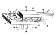
図1には、第1実施形態例のパッケージモジュールが分解状態により示されている。このパッケージモジュール1は、回路基板2と、当該回路基板2を収容するためのケース3を構成する蓋側ケース部4および基部ケース部5と、アダプタ6とを有して構成されている。
【0012】
この第1実施形態例のパッケージモジュール1は光通信用モジュールであり、回路基板2には、図2に示されるように、後述する光モジュール(サブモジュール)10が搭載されると共に、IC部品や抵抗素子やコンデンサ素子などの回路部品11が搭載されている。また、回路基板2には、光モジュール10と回路部品11間や、回路部品11同士を接続するための配線パターン12などが形成されて回路が構成されている。さらに、この第1実施形態例では、回路基板2の表面の少なくとも端縁部分にグランドパターン13が形成されている。さらにまた、回路基板2には、当該回路基板2に形成されている回路とパッケージモジュール1の外部とを電気的に接続させるための端子ピン14が取り付けられている。グランドパターン13は、例えば、端子ピン14を介して、外部のグランドに接地することができる構成となっている。
【0013】
光モジュール10は、ケース15の内部に、光を電気に変換する変換部と、電気を光に変換する変換部とのうちの少なくとも一方の変換部を収容配置したものである。つまり、光モジュール10のケース15の内部には、発光素子(例えばレーザダイオード(LD))と受光素子(例えばフォトダイオード(PD))とのうちの少なくとも一方(図示せず)が配設されている。また、ケース15には当該ケース15の外側から内側に貫通する貫通孔(図示せず)が形成されており、この貫通孔にはフェルール16が挿通され当該フェルール16はケース15に固定されている。フェルール16には貫通孔(図示せず)が設けられ、当該貫通孔には光ファイバ17が挿通され当該光ファイバ17の先端がケース15の内部に露出している。この光ファイバ17の先端は、当該光ファイバ17と、発光素子又は受光素子とが設定の良好な光結合状態となるように調整されて配置されている。
【0014】
光モジュール10においては、例えば、受光素子が設けられている場合には、光ファイバ17の先端から光が出射されると、その出射光が受光素子に入射して、受光素子は、その入射光に応じた電気信号を出力する。つまり、光信号が電気信号に変換される。また、発光素子が設けられている場合には、電気信号に応じて発光素子が発光すると、その放射光が光ファイバ17の先端から光ファイバ内部に入射し光ファイバ17を伝搬する。つまり、電気信号が光信号に変換される。
【0015】
このような光モジュール10が設けられる回路基板2には、回路部品11として、例えば、光モジュール10に内蔵されている発光素子の動作状態を制御するためのIC部品や、受光素子から出力された電気信号を増幅するアンプなどが搭載される。なお、もちろん、それ以外の電子部品も回路部品11として、回路基板2に搭載される場合がある。回路基板2に搭載される回路部品11は、特に限定されるものではなく、必要に応じて、適宜選択されるものである。
【0016】
パッケージモジュール1のアダプタ6は、パッケージモジュール1に接続する光コネクタと嵌合する態様を有している。また、アダプタ6には、回路基板2上の光モジュール10から引き出されたフェルール16が固定される。つまり、光ファイバ17の端部がアダプタ6に固定される。当該アダプタ6は、光コネクタが嵌合接続することにより、その光コネクタに固定されている光ファイバと、光ファイバ17とが光結合する構成となっている。なお、アダプタ6に嵌合可能な光コネクタの例を挙げれば、例えば、SCコネクタと呼ばれるものや、MUコネクタと呼ばれるものや、LCコネクタと呼ばれるもの等がある。
【0017】
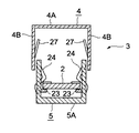
この第1実施形態例では、ケース3は、図1に示されるような蓋側ケース部4と基部ケース部5を有して構成されている。蓋側ケース部4は、回路基板2の表面に対向する頂壁部4Aと、この頂壁部4Aに立設する側壁部4Bとを有して構成されている。また、基部ケース部5は、回路基板2の裏面に対向する底壁部5Aと、この底壁部5Aに立設する側壁部5Bとを有して構成されている。それら蓋側ケース部4と基部ケース部5は導体により構成されており、蓋側ケース部4の側壁部4Aを基部ケース部5の側壁部5Bの外側面に沿わせて嵌合させることで蓋側ケース部4と基部ケース部5を組み合わせてケース3と成す。なお、図1の例では、蓋側ケース部4の側壁部4Bには開口部20が設けられ、また、蓋側ケース部4と基部ケース部5の側壁部4B,5B同士が嵌合した際に側壁部4Bの開口部20の形成位置に対応する側壁部5B部分には突出部21が形成されている。蓋側ケース部4と基部ケース部5が嵌め合うことにより、側壁部5Bの突出部21が側壁部4Bの開口部20に嵌って抜け止め状態となり、蓋側ケース部4と基部ケース部5の嵌合状態が維持される。
【0018】
基部ケース部5の側壁部5Bにはケース内側に向けて突出する回路基板支持用突出部23が形成されている。この第1実施形態例では、その回路基板支持用突出部23は側壁部5Bの一部の先端側を折り曲げて作製されている。図1(c)の断面図に示すように、回路基板支持用突出部23は、その上面が回路基板2の裏面に当接して回路基板2を基部ケース部5の底壁部5Aに対して浮いた状態で支持する。
【0019】
この第1実施形態例では、回路基板支持用突出部23は複数箇所に点在配置されている。つまり、図1では後ろ側に配置されている側壁部5B部分において、左右両側の側端部に、それぞれ、回路基板支持用突出部23(23a,23b)が形成されている。また、図1では右側に配置されている側壁部5B部分と、左側に配置されている側壁部5B部分とのそれぞれに回路基板支持用突出部23(23c,23d)が形成されている。その右側の回路基板支持用突出部23cと、左側の回路基板支持用突出部23dとは、対向し合う位置に配置されている。この第1実施形態例では、回路基板支持用突出部23による回路基板2の支持を安定化させるために、回路基板支持用突出部23a,23bは、支持する回路基板2の長手方向の中心線に対して対称的な位置にそれぞれ配設されると共に、回路基板支持用突出部23c,23dも同様に、支持する回路基板2の長手方向の中心線に対して対称的な位置にそれぞれ配設されている。
【0020】
また、この第1実施形態例では、複数の回路基板支持用突出部23によって、回路基板2が基部ケース部5の底壁部5Aと平行な状態で支持されるように、複数の回路基板支持用突出部23の上面の高さ位置が揃えられている。つまり、それら回路基板支持用突出部23の上面は、底壁部5Aと平行な同一平面上に配置形成されている。
【0021】
基部ケース部5の側壁部5Bには、ケース内側に突出するはね板24が形成されている。この第1実施形態例では、はね板24は、左右両側の側壁部5B部分にそれぞれ、回路基板支持用突出部23により支持されている回路基板2の長手方向の中心線に対して対称となる位置に配置されている。
【0022】
それらはね板24は、側壁部5Bを切り起こし加工して作製されるものであり、図1(b)の断面図に示されるような内向き斜面部位24Aと、外向き斜面部位24Bとを有して構成されている。
【0023】
はね板24の内向き斜面部位24Aは、回路基板2の収容入口側(側壁部5Bの上部側)から底壁部5A側に向かうに従って側壁部5Bからケース内側に離れる方向(内向き)の傾きを備えている。また、外向き斜面部位24Bは、内向き斜面部位24Aの下端側から側壁部5Bに戻る方向(外向き)に傾けられている。
【0024】
この第1実施形態例では、はね板24の内向き斜面部位24Aは、基端部分Kを固定部として、側壁部5Bに対する傾きを変化させることができるものである。この第1実施形態例では、左右両側のはね板24の内向き斜面部位24A間の間隔は、回路基板2の幅よりも狭くなっているが、図1(b)に示されるように、回路基板2の裏面を基部ケース部5の底壁部5Aに向けて、基部ケース部5の収容入口側(上方側)から回路基板2を基部ケース部5の内部に挿入していき回路基板2の端面がはね板24の内向き斜面部位24Aに当接しても、さらに、回路基板2を押し込むことにより、その回路基板2から内向き斜面部位24Aへの押圧力によって、左右両側の内向き斜面部位24A間の間隔を広げる方向に内向き斜面部位24Aの傾きが変化して回路基板2を底壁部5A側に押し進めることができる。
【0025】
また、図1(c)の断面図に示されるように、回路基板2が回路基板支持用突出部23に支持されている状態で、はね板24の外向き斜面部位24Bは、その回路基板2の表面を弾性力を利用して押圧する構成となっている。つまり、当該外向き斜面部位24Bは、回路基板表面押圧部として機能する。この第1実施形態例では、その外向き斜面部位24Bが回路基板2の表面のグランドパターン13に押圧接触するように、はね板24とグランドパターン13は関連づけられて、それらの形成位置が設定されている。
【0026】
このようなはね板24と、回路基板支持用突出部23とによって、回路基板2は表裏両側から挟持されてケース3(基部ケース部5)に固定される。なお、基部ケース部5には、回路基板2に取り付けられている端子ピン14をケース内部から外側に突き出すための開口部26が形成されている。
【0027】
この第1実施形態例のパッケージモジュール1は上記のように構成されている。このため、パッケージモジュール1の組み立て工程において、回路基板2を基部ケース部5の上方側から底壁部5A側に向けてケース内部に挿入し押し込むだけで、回路基板2を基部ケース部5に固定させることができる。つまり、この第1実施形態例の構成を備えることによって、回路基板2の基部ケース部5への取り付けの自動化が容易となる。
【0028】
また、この第1実施形態例では、弾性力を利用して回路基板2を表裏両側から挟持して基部ケース部5に固定する構成であり、回路基板2が熱膨張した際に、その膨張に因る基板の撓みを逃がすことができる構造となっている。このため、熱膨張に起因した回路基板2の撓み変形を防止することができる。この第1実施形態例では、回路基板2には、光ファイバ17と、受光素子又は発光素子との光結合部が配置されており、回路基板2が僅かに撓み変形しただけで、それら光ファイバ17と、素子との光軸がずれて光結合状態が悪化してしまう虞がある。これに対して、この第1実施形態例では、熱膨張に起因した回路基板2の撓み変形を防止することができるので、そのような回路基板2の熱膨張に起因した光結合状態の悪化を回避することができる。
【0029】
さらに、この第1実施形態例では、回路基板2の表面に形成されているグランドパターン13は例えば回路基板2の端子ピン14を介して外部のグランドに接地されるものである。はね板24はグランドパターン13に押圧接触するので、このはね板24とグランドパターン13の押圧接触により、はね板24を通して基部ケース部5全体がグランド電位となる。また、基部ケース部5と蓋側ケース部4の嵌合によって、蓋側ケース部4は基部ケース部5に接触する部位を有しているので、その接触部位を介して蓋側ケース部4もグランド電位を持つものとなる。これにより、蓋側ケース部4と基部ケース部5から成るケース3は、電磁波シールド部として効果的に機能することができる。
【0030】
さらにまた、この第1実施形態例では、蓋側ケース部4と、基部ケース部5と、はね板24とは導体により形成されており、熱伝導が良いものであることから、回路基板2に形成されている回路から発生した熱は、グランドパターン13とはね板24の押圧接触部分から蓋側ケース部4と基部ケース部5に伝熱され外部に放出することができる。つまり、蓋側ケース部4および基部ケース部5を放熱部として機能させることができる。
【0031】
上記のように、この第1実施形態例の構成を備えることによって、回路基板2の熱膨張に起因した光結合状態の悪化防止効果と、ケース3による電磁波シールド効果および放熱の促進効果とによって、パッケージモジュール1への環境変動の悪影響が軽減されて、回路基板2の回路動作のより一層の安定化を図ることができる。したがって、パッケージモジュール1の信頼性を向上させることができる。
【0032】
以下に、第2実施形態例を説明する。なお、この第2実施形態例の説明において、第1実施形態例と同一構成部分には同一符号を付し、その共通部分の重複説明は省略する。
【0033】
この第2実施形態例では、図3(a)の断面図に示されるように、はね板24の外向き斜面部位(回路基板表面押圧部)24Bが回路基板2の表面を押圧しているときに、はね板24の外向き斜面部位24Bの先端側が基部ケース部5の側壁部5Bよりも外側に食み出す構成となっている。
【0034】
そのはね板24の外側への食み出し量は、図3(b)の断面図に示されるように、蓋側ケース部4の側壁部4Bが当該はね板24の食み出し部分を押圧しながら蓋側ケース部4と基部ケース部5の側壁部4B,5Bが嵌合できるように設定されている。
【0035】
このため、蓋側ケース部4と基部ケース部5が組み合わされることにより、蓋側ケース部4の側壁部4Bが、はね板24の外側への食み出し部分を押圧する。この押圧力ははね板24から、回路基板支持用突出部23に支持されている回路基板2に作用する。これにより、回路基板2には、はね板24自体からの押圧力に加えて、蓋側ケース部4の側壁部4Bからの押圧力が加えられることになり、第1実施形態例の構成よりも強い押圧力をはね板24から回路基板2に作用させることができる。つまり、回路基板2をケース3(基部ケース部5)に固定させる力を強めることができる。
【0036】
ところで、外向き斜面部位24Bの先端部が、外向きの状態のまま、基部ケース部5の側壁部5Bの外側に食み出す形態としてもよいが、そのような形態にすると、蓋側ケース部4と基部ケース部5の側壁部4B,5Bを嵌合する際に、はね板24の外向き斜面部位24Bの先端角部が蓋側ケース部4の側壁部4Bに局所的に当接することになり、その外向き斜面部位24Bの先端角部から側壁部4Bの局所的な当接部分に大きな力が作用する。これに起因して蓋側ケース部4と基部ケース部5の嵌合作業に大きな力を要する等の問題が発生する虞がある。
【0037】
このことを考慮して、この第2実施形態例では、はね板24の外向き斜面部位24Bの先端部分を内向きに曲げ加工し、その曲げ部が基部ケース部5の側壁部5Bの外側に食み出す構成としている。これにより、蓋側ケース部4と基部ケース部5の側壁部4B,5Bを嵌合する際に、蓋側ケース部4の側壁部4Bには、はね板24の曲面部分が当接することになり、側壁部4Bとはね板24との当接面積が増加する結果、はね板24から側壁部4Bへの作用力を分散することができて、例えば、蓋側ケース部4と基部ケース部5の嵌合作業を容易にすることができる。
【0038】
なお、この発明は第1や第2の各実施形態例の構成に限定されるものではなく、様々な実施の形態を採り得る。例えば、第1や第2の各実施形態例の構成に加えて、図4の断面図に示されるように、蓋側ケース部4の側壁部4Bの内壁面に、はね板27を設ける構成としてもよい。そのはね板27は、側壁部4Bの先端側から頂壁部4A側に向かうに従ってケース内側に離れる方向の傾きを持つものである。このはね板27は、蓋側ケース部4と基部ケース部5の側壁部4B,5Bを嵌合したときに、弾性力を利用して基部ケース部5の側壁部5Bを押圧する構成となっている。そのはね板27による基部ケース部5の側壁部5Bへの押圧接触によって、例えばはね板27を導体で構成することにより、蓋側ケース部4と基部ケース部5を確実に導通することができて、回路基板2側から基部ケース部5を介して蓋側ケース部4をより確実にグランド電位とすることができる。これにより、蓋側ケース部4による電磁波シールド効果の信頼性を高めることができる。また、放熱効果も高めることができる。
【0039】
また、第1や第2の各実施形態例では、回路基板支持用突出部23は、はね板24とは別体であったが、例えば、はね板24を図5の断面図に示されるような形態とすることによって、はね板24の一部を回路基板支持用突出部として機能させてもよい。このような場合には、第1や第2の各実施形態例に示した回路基板支持用突出部23を省略してもよい。つまり、図5に示すはね板24は、回路基板表面押圧部として機能する部分よりも先端側の部位が、回路基板2の端面から裏面に回り込む形態に曲げ加工され、当該はね板24の先端側部位は回路基板2の裏面に当接する態様となっている。その回路基板2の裏面に当接するはね板24の部分Zが回路基板支持用突出部として機能する。
【0040】
さらに、第1や第2の各実施形態例では、蓋側ケース部4と基部ケース部5とはね板24は、導体により構成されていたが、例えば、それらは樹脂等の絶縁体により構成され、その表面全体が導体によりコーティングされている構成としてもよい。
【0041】
さらに、はね板24は、基部ケース部5の側壁部5Bの切り起こし加工により作製されるものであったが、例えば、側壁部5Bとは別体のはね板24を、側壁部5Bに例えば溶接などによって接合する構成としてもよい。また回路基板支持用突出部23に関しても同様に、第1や第2の各実施形態例では回路基板支持用突出部23は基部ケース部5の側壁部5Bの折り曲げ加工により作製されていたが、例えば、回路基板支持用突出部23を基部ケース部5に溶接などによって接合する構成としてもよい。このように回路基板支持用突出部23が基部ケース部5とは別部材により構成されている場合には、回路基板支持用突出部23は絶縁体だけで構成してもよい。
【0042】
さらに、第1や第2の各実施形態例では、回路基板支持用突出部23は、回路基板2の端縁部分だけに当接する構成であったが、例えば、左右両側の側壁部5Bを掛け渡すような形態の回路基板支持用突出部23を設けてもよい。この場合には、例えば、回路基板2に形成されている回路の短絡トラブルを防止するために、回路基板支持用突出部23は絶縁体により構成することがよい。
【0043】
さらに、回路基板支持用突出部23の配置位置は、第1や第2の各実施形態例に示した位置に限定されるものではなく、例えば、図6(a)の模式図に示されるように、はね板24の配置位置を中心とした前後両側に対称的に回路基板支持用突出部23を配置してもよい。さらに、図6(b)の模式図に示されるように、はね板24の下方側に回路基板支持用突出部23を配置してもよい。さらに、第1や第2の各実施形態例では、回路基板2の長手方向の中心線に対して左右両側に対称的に回路基板支持用突出部23が配置されていたが、回路基板2の左右両側に非対称に回路基板支持用突出部23を配置してもよい。
【0044】
さらに、回路基板支持用突出部23は、基部ケース部5の側壁部5Bからケース内側に突出する構成であったが、例えば、図6(c)に示されるように、基部ケース部5の底壁部5Aから上側に突出する形態としてもよい。
【0045】
さらに、第1や第2の各実施形態例では、はね板24が押圧する回路基板2の表面部分にグランドパターン13が形成されていたが、例えば、基部ケース部5をグランドに接地する必要がない場合や、他の手段によって基部ケース部5がグランドに接地される場合には、はね板24が押圧する回路基板2の表面部分にグランドパターン13が形成されていなくともよい。換言すれば、はね板24は、回路基板2の表面部分における絶縁体部分を押圧する構成としてもよい。
【0046】
さらに、第1や第2の各実施形態例では、光通信用モジュールを例にして説明したが、この発明は、回路基板がケース内に収容配置されているパッケージモジュールであれば適用することができるものであり、例えば、VCO(Voltage Controlled Oscillator)やデュプレクサ等の高周波回路が形成されている高周波回路モジュールにも適用することができる。また、例えば低周波電流や直流電流が通電する回路が形成されている回路基板がケースに収容されて成るモジュールにも、本発明は適用することができるものである。
【0047】
【発明の効果】
この発明によれば、ケースの内部に回路基板を支持する回路基板支持用突出部が設けられると共に、ケースの両側の対向する側壁部にはケース内側に突出するはね板が設けられており、はね板と回路基板支持用突出部によって、回路基板を表裏両側から挟持してケースに固定する構成とする。そのはね板は、ケースの回路基板収容入口側から底壁部側に向かうに従って側壁部からケース内側に離れる方向の傾きを持つ内向き斜面部位と、この内向き斜面部位の下端側から側壁部に戻る方向に傾けた外向き斜面部位とを有し、外向き斜面部位が弾性力を利用して回路基板の表面を押圧する回路基板表面押圧部と成している。
【0048】
このような構成を有しているので、次に示すように回路基板をケースに収容することができる。例えば、まず、ケースの回路基板収容入口から回路基板を挿入し、ケース内部に入り込ませる。この後も、引き続き回路基板をケースの底壁部側に向けて挿入していくと、回路基板は、はね板の内向き斜面部位に当接するが、さらに回路基板にケースの底壁部側に向かう方向の力を加えていくことにより、回路基板がはね板の内向き斜面部位を押圧しはね板は側壁部側に向けて傾きが変化する。このため、回路基板はケースの底壁部側に向けて押し進むことができる。その後、回路基板が回路基板支持用突出部に当接したときに、回路基板の押し込みを終了する。このとき、回路基板からはね板の内向き斜面部位への押圧は解除されてはね板の傾きは回復しており、これにより、はね板の外向き斜面部位が回路基板の表面を押圧する。したがって、はね板の外向き斜面部位と回路基板支持用突出部によって、弾性力を利用して、回路基板が表裏両面側から挟持されて固定される。
【0049】
このように、回路基板をケースの回路基板収容入口側からケース内部に挿入し、当該回路基板を回路基板支持用突出部に当接するまで押し込むだけで、非常に簡単に回路基板をケースに取り付け固定することができる。よって、回路基板のケースへの取り付け作業の自動化が容易となる。
【0050】
また、回路基板を表裏両面側から弾性力を利用して挟持固定する構成であるために、何らかの原因によって、回路基板をケースから取り外さなければならないときに、その取り外し作業が容易である。
【0051】
さらに、回路基板を表裏両面側から弾性力を利用して挟持固定する構成であるために、例えば、回路基板が熱膨張した際に、その膨張による基板の伸びを逃がすことができて熱膨張に起因した回路基板の撓みを防止することができる。回路基板が撓んでしまうと、その撓みに起因して例えば電子部品と回路基板間の接合が損傷し、これにより、電子部品が回路基板から外れてしまうという問題が発生する虞があるが、この発明では、熱膨張に起因した回路基板の撓みを防止できるので、そのような回路基板の撓みに因る問題を回避することができる。特に、パッケージモジュールが光通信用モジュールである場合には、そのような回路基板の撓みは問題となる。つまり、光通信用モジュールは、光ファイバと、発光素子あるいは受光素子との光結合部分が回路基板上に配置されており、回路基板が僅かでも撓んでしまうと、その光結合状態が悪化してしまう虞がある。これに対して、この発明の構成を備えることにより、そのような熱膨張に因る回路基板の撓みに起因した光結合状態の悪化を防止することができて、光通信用モジュールの信頼性を向上させることができる。
【0052】
さらに、この発明では、回路基板支持用突出部は、回路基板をケースの底壁部に対して浮いた状態で支持するので、回路基板の裏面とケースの底壁部との間に空間が形成されることになり、これにより、回路基板の裏面にも電子部品などを搭載することができる。このことから、回路基板の裏面も有効に利用することができることとなり、これにより、回路基板を小型化することができ、これに伴いパッケージモジュールの小型化を図ることができる。
【0053】
さらに、はね板の外向き斜面部位が回路基板の表面を押圧するので、つまり、はね板は、面でもって回路基板の表面を押圧するので、はね板と回路基板表面との接触面積を増加させることができる。これにより、回路基板の挟持力を強めることができるし、また、回路基板の局所的な部分に力が作用して回路基板が撓んで前記したような問題が発生してしまうことを回避することができる。
【0054】
はね板の少なくとも表面部分と、ケースの少なくとも表面部分とが導体により形成されており、回路基板の表面には、少なくともはね板の回路基板表面押圧部が押圧する部分に、グランドパターンが形成されているものにあっては、はね板の回路基板表面押圧部と回路基板のグランドパターンとの押圧接触によって、ケース表面は、はね板と回路基板のグランドパターンを介してグランドに接地することができる。これにより、ケースは、電磁波シールド部として機能することができる。例えば、パッケージモジュールを構成する回路基板に高周波回路が形成されている高周波回路モジュールや光通信用モジュールの場合には、ケースによって、外部からケース内部の高周波回路に侵入する電磁波をカットできるので、回路動作の安定化を図ることができる。
【0055】
また上記同様に、回路基板の回路から発生した熱を回路基板のグランドパターンからはね板を介してケースの表面に伝熱することができるので、熱をケース表面から放熱させることが可能である。これにより、回路基板の回路の温度上昇を抑制することができて、熱による回路動作不良を回避することができて、回路動作の信頼性を高めることができる。
【0056】
はね板は、回路基板の配置領域の両側に間隔を介して配置されると共に、回路基板支持用突出部も回路基板の配置領域の両側に間隔を介して配置されているものにあっては、回路基板を安定的に固定することができる。
【0057】
はね板がケースの側壁部の切り起こし加工により作製されているものにあっては、はね板を容易に作製することができ、パッケージモジュールの製造効率を高めることができる。
【0058】
ケースは、基部ケース部と蓋側ケース部の側壁部同士を嵌合して組み合わせる構成とし、基部ケース部の側壁部に設けられているはね板は、その回路基板表面押圧部よりも先端側の部位が、基部ケース部の側壁部よりも外側に食み出す形態と成し、基部ケース部と蓋側ケース部が嵌め合った状態において、蓋側ケース部の側壁部が、はね板の先端側の食み出し部分を基部ケース部の内側に向けて押圧する構成のものにあっては、蓋側ケース部の側壁部が、はね板の先端側の食み出し部分を基部ケース部の内側に向けて押圧することによって、その押圧力がはね板から回路基板に作用してはね板による回路基板の押圧力を強めることができる。したがって、回路基板を挟持固定する力が強くなり、回路基板をより強固にケースに取り付けることができる。
【0059】
また、はね板と、蓋側ケース部の側壁部とが押圧接触することによって、例えば、はね板を介して、基部ケース部と蓋側ケース部を確実に電気的および熱的に接続させることができる。これにより、例えば、回路基板のグランドパターンとはね板を介して基部ケース部だけでなく蓋側ケース部も確実にグランドに接地させることができて、蓋側ケース部および基部ケース部を電磁波シールド部としてより確実に機能させることができる。また、回路基板の回路の発熱を同様にグランドパターンとはね板を介して蓋側ケース部に確実に伝熱させて外部に放熱させることができる。
【0060】
蓋側ケース部の側壁部の内壁面に、はね板が設けられ、蓋側ケース部と基部ケース部との側壁部同士の嵌合状態において、蓋側ケース部の側壁部のはね板は、弾性力を利用して、基部ケース部の側壁部を押圧して接触するものにあっても、その蓋側ケース部のはね板によって、蓋側ケース部と基部ケース部とを確実に、電気的および熱的に接続させることができることから、上記同様の効果を得ることができる。
【0061】
はね板の回路基板表面押圧部よりも先端側部位が、回路基板の端面から裏面に回り込む形態に曲げ加工され、当該はね板の先端側部位が回路基板支持用突出部として機能する構成のものにあっては、はね板と別に回路基板支持用突出部を設けなくて済むので、ケースの形態を簡素化することができる。また、ケースの製造工程の簡略化を図ることができる。
【図面の簡単な説明】
【図1】第1実施形態例のパッケージモジュールを説明するための図である。
【図2】第1実施形態例のパッケージモジュールのケースに内蔵される回路基板の一構成例を模式的に示したモデル図である。
【図3】第2実施形態例を説明するための図である。
【図4】その他の実施形態例を説明するためのモデル図である。
【図5】さらに別のその他の実施形態例を説明するためのモデル図である。
【図6】回路基板支持用突出部のその他の例を説明するための図である。
【図7】光送受信モジュールの一例を示すモデル図である。
【符号の説明】
1 パッケージモジュール
2 回路基板
3 ケース
4 蓋側ケース部
5 基部ケース部
13 グランドパターン
23 回路基板支持用突出部
24,27 はね板[0001]
TECHNICAL FIELD OF THE INVENTION
The present invention relates to a package module having a circuit board housed in a case.
[0002]
[Background Art]
FIG. 7 is a schematic cross-sectional view showing an example of a package module (see Patent Document 1). This package module is an optical transceiver module. In this optical transceiver module 30, a circuit board 31 is accommodated and arranged inside a case 32.
[0003]
An electronic component 33 is mounted on the circuit board 31, and a wiring pattern (not shown) and the like are formed to constitute a circuit. The circuit board 31 is a multilayer board including a ground layer. The circuit board 31 is provided with a hole 34 penetrating from the front side to the back side, and a conductor film 35 is formed on an inner wall surface of the hole 34. Is formed. A pin 37 is inserted from the outside of the case 32 toward the inside through a through hole 36 formed in the wall of the case 32, and a tip end of the pin 37 is a hole of the circuit board 31 housed inside the case. 34. The pins 37 and the circuit board 31 are fixed by solder. Further, a projection 38 is formed on the pin 37, and the projection 38 is engaged with the surface of the case 32.
[0004]
The circuit board 31 is fixed to the case 32 by the locking of the projecting portion 38 of the pin 37 and the soldering of the pin 37 and the circuit board 31. Further, by grounding the pin 37 to an external ground, the ground layer of the circuit board 31 is grounded to the ground via the conductive film 35 of the hole 34 and the pin 37.
[0005]
[Patent Document 1]
Japanese Utility Model Publication No. 2-118969
[Patent Document 2]
JP-A-9-270747
[Patent Document 3]
JP 2000-151173 A
[Patent Document 4]
JP-A-9-181466
[0006]
[Problems to be solved by the invention]
In the optical transceiver module 30 shown in FIG. 7, in the step of housing and fixing the circuit board 31 inside the case 32, for example, the circuit board 31 is housed inside the case 32, and the hole 34 of the circuit board 31 and the case 32 Is aligned with the through hole 36 of FIG. Then, the pin 37 is inserted into the through hole 36 and the hole 34 from the outside of the case 32 until the protrusion 38 is locked to the surface of the case 32. Thereafter, the pins 37 are soldered to the circuit board 31 while maintaining the state, and the circuit board 31 is fixed to the case 32.
[0007]
Such an operation of accommodating and fixing the circuit board 31 in the case 32 is very difficult to automate, and there is a problem that improvement in manufacturing efficiency is limited. Further, the circuit board 31 is fixed to the case 32 by solder, and the position of the soldered portion of the circuit board 31 is fixed, so that when the circuit board 31 thermally expands, Since the expansion of the substrate due to thermal expansion cannot be released, a part of the circuit substrate 31 is bent. The bending of the circuit board 31 may cause a problem that, for example, a joint (for example, a solder joint) between the circuit board 31 and the electronic component 33 is damaged.
[0008]
The present invention has been made to solve the above-described problems, and an object of the present invention is to easily automate a work of attaching a circuit board to a case, and to release a deflection caused by thermal expansion of the circuit board. An object of the present invention is to provide a package module having a configuration that can be performed.
[0009]
[Means for Solving the Problems]
In order to achieve the above object, the present invention provides means for solving the above problems with the following configuration. In other words, the present invention provides a package module in which a circuit board is housed in a case. In the case, the circuit board is abutted against the back surface of the circuit board to support the circuit board in a floating state with respect to the bottom wall of the case. A circuit board supporting protrusion is provided, and a splash plate projecting inward of the case is provided on opposing side walls on both sides of the case, and the splash plate is provided at the bottom from the circuit board housing entrance side of the case. There is an inward slope portion inclined in a direction away from the side wall portion toward the inside of the case toward the wall portion, and an outward slope portion inclined in a direction returning from the lower end side of the inward slope portion to the side wall portion. The outwardly sloped portion forms a circuit board surface pressing portion that presses the surface of the circuit board supported by the circuit board supporting projection using elastic force, and the circuit board surface pressing portion is used. Department and front By the circuit board supporting protrusions, and characterized in that it is fixed by being sandwiched the circuit board from the front and back both sides in the case.
[0010]
BEST MODE FOR CARRYING OUT THE INVENTION
Hereinafter, embodiments of the present invention will be described with reference to the drawings.
[0011]
FIG. 1 shows the package module of the first embodiment in an exploded state. The package module 1 includes a circuit board 2, a lid-side case 4 and a base case 5 constituting a case 3 for housing the circuit board 2, and an adapter 6.
[0012]
The package module 1 of the first embodiment is an optical communication module, and an optical module (sub-module) 10 described later is mounted on a circuit board 2 as shown in FIG. Circuit components 11 such as a resistance element and a capacitor element are mounted. A circuit is formed on the circuit board 2 by forming a wiring pattern 12 between the optical module 10 and the circuit component 11 or connecting the circuit components 11 to each other. Further, in the first embodiment, a ground pattern 13 is formed on at least an edge portion of the surface of the circuit board 2. Furthermore, terminal pins 14 for electrically connecting a circuit formed on the circuit board 2 to the outside of the package module 1 are attached to the circuit board 2. The ground pattern 13 is configured to be able to be grounded to an external ground via, for example, a terminal pin 14.
[0013]
The optical module 10 accommodates and arranges at least one of a conversion unit that converts light into electricity and a conversion unit that converts electricity into light inside a case 15. That is, at least one (not shown) of a light emitting element (for example, a laser diode (LD)) and a light receiving element (for example, a photodiode (PD)) is disposed inside the case 15 of the optical module 10. I have. The case 15 has a through hole (not shown) penetrating from the outside to the inside of the case 15. A ferrule 16 is inserted into the through hole, and the ferrule 16 is fixed to the case 15. . A through hole (not shown) is provided in the ferrule 16, and an optical fiber 17 is inserted into the through hole, and the tip of the optical fiber 17 is exposed inside the case 15. The tip of the optical fiber 17 is arranged so as to be adjusted so that the optical fiber 17 and the light emitting element or the light receiving element are in a well-set optical coupling state.
[0014]
In the optical module 10, for example, when a light receiving element is provided, when light is emitted from the tip of the optical fiber 17, the emitted light enters the light receiving element, and the light receiving element And outputs an electric signal corresponding to. That is, the optical signal is converted into an electric signal. In the case where a light emitting element is provided, when the light emitting element emits light in response to an electric signal, the emitted light enters the inside of the optical fiber from the tip of the optical fiber 17 and propagates through the optical fiber 17. That is, an electric signal is converted into an optical signal.
[0015]
On the circuit board 2 on which such an optical module 10 is provided, as the circuit component 11, for example, an IC component for controlling an operation state of a light emitting element built in the optical module 10 or an output from a light receiving element is provided. An amplifier for amplifying electric signals is mounted. Of course, other electronic components may be mounted on the circuit board 2 as the circuit components 11. The circuit component 11 mounted on the circuit board 2 is not particularly limited, and is appropriately selected as needed.
[0016]
The adapter 6 of the package module 1 has a mode of fitting with an optical connector connected to the package module 1. Further, a ferrule 16 drawn from the optical module 10 on the circuit board 2 is fixed to the adapter 6. That is, the end of the optical fiber 17 is fixed to the adapter 6. The adapter 6 is configured such that an optical fiber fixed to the optical connector and the optical fiber 17 are optically coupled by fitting and connecting the optical connector. In addition, examples of the optical connector that can be fitted to the adapter 6 include, for example, a connector called an SC connector, a connector called an MU connector, and a connector called an LC connector.
[0017]
In the first embodiment, the case 3 includes a lid-side case 4 and a base case 5 as shown in FIG. The lid case 4 includes a top wall 4A facing the surface of the circuit board 2 and a side wall 4B standing upright on the top wall 4A. Further, the base case 5 includes a bottom wall 5A facing the back surface of the circuit board 2 and a side wall 5B standing upright on the bottom wall 5A. The lid-side case portion 4 and the base case portion 5 are made of a conductor, and the side wall portion 4A of the lid-side case portion 4 is fitted along the outer surface of the side wall portion 5B of the base case portion 5 so as to be fitted. The case 3 is formed by combining the side case 4 and the base case 5. In the example of FIG. 1, an opening 20 is provided in the side wall 4 </ b> B of the lid case 4, and when the lid 4 and the side walls 4 </ b> B of the base case 5 are fitted together. A protrusion 21 is formed on the side wall 5B corresponding to the position where the opening 20 of the side wall 4B is formed. When the lid case 4 and the base case 5 are fitted to each other, the protrusion 21 of the side wall 5B fits into the opening 20 of the side wall 4B to be in a retaining state. The fitted state is maintained.
[0018]
A circuit board supporting protrusion 23 protruding toward the inside of the case is formed on the side wall 5B of the base case 5. In the first embodiment, the circuit board supporting projection 23 is formed by bending a part of the side wall 5B at the front end. As shown in the cross-sectional view of FIG. 1C, the upper surface of the circuit board supporting protrusion 23 is in contact with the back surface of the circuit board 2, and the circuit board 2 is moved with respect to the bottom wall 5 </ b> A of the base case 5. Support in a floating state.
[0019]
In the first embodiment, the circuit board supporting projections 23 are scattered at a plurality of locations. That is, in the side wall portion 5B located on the rear side in FIG. 1, the circuit board supporting protrusions 23 (23a, 23b) are formed at the left and right side end portions, respectively. In FIG. 1, the circuit board supporting protrusions 23 (23c, 23d) are formed on each of the side wall 5B disposed on the right side and the side wall 5B disposed on the left. The right circuit board supporting projection 23c and the left circuit board supporting projection 23d are arranged at positions facing each other. In the first embodiment, in order to stabilize the support of the circuit board 2 by the circuit board supporting projections 23, the circuit board supporting projections 23a and 23b are provided with a longitudinal center line of the circuit board 2 to be supported. And the circuit board supporting protrusions 23c and 23d are also similarly disposed at positions symmetric with respect to the longitudinal center line of the circuit board 2 to be supported. Have been.
[0020]
Further, in the first embodiment, the plurality of circuit board supporting protrusions 23 support the plurality of circuit board supporting members so that the circuit board 2 is supported in parallel with the bottom wall 5A of the base case part 5. The height positions of the upper surfaces of the projecting portions 23 are aligned. That is, the upper surfaces of the circuit board supporting projections 23 are formed on the same plane parallel to the bottom wall 5A.
[0021]
A splash plate 24 protruding inside the case is formed on the side wall 5B of the base case 5. In the first embodiment, the splash plate 24 is symmetrical with respect to the longitudinal center line of the circuit board 2 supported by the circuit board supporting protrusions 23 on the left and right side walls 5B. It is located at a position.
[0022]
The splash plates 24 are made by cutting and erecting the side wall portion 5B, and include an inward slope portion 24A and an outward slope portion 24B as shown in the cross-sectional view of FIG. It is configured to have.
[0023]
The inward slope portion 24A of the splash plate 24 has a direction (inward) away from the side wall portion 5B toward the inside of the case from the accommodation entrance side (upper side of the side wall portion 5B) to the bottom wall portion 5A side of the circuit board 2. It has a tilt. The outward slope portion 24B is inclined in a direction (outward) to return to the side wall portion 5B from the lower end of the inward slope portion 24A.
[0024]
In the first embodiment, the inwardly inclined surface portion 24A of the splash plate 24 can change its inclination with respect to the side wall portion 5B with the base end portion K as a fixed portion. In the first embodiment, the interval between the inwardly inclined portions 24A of the splash plates 24 on both the left and right sides is smaller than the width of the circuit board 2, but as shown in FIG. With the back surface of the circuit board 2 facing the bottom wall 5A of the base case 5, the circuit board 2 is inserted into the inside of the base case 5 from the accommodation entrance side (upper side) of the base case 5. Even if the end surface of the plate abuts against the inward slope portion 24A of the splash plate 24, the circuit board 2 is further pushed in, and the pressing force from the circuit board 2 to the inward slope portion 24A causes the inward of the left and right sides. The inclination of the inward slope portion 24A changes in the direction of increasing the interval between the slope portions 24A, and the circuit board 2 can be pushed toward the bottom wall 5A.
[0025]
Further, as shown in the cross-sectional view of FIG. 1C, when the circuit board 2 is supported by the circuit board supporting projection 23, the outwardly sloping portion 24B of the splash plate 24 is mounted on the circuit board. 2 is pressed by utilizing elastic force. That is, the outward slope portion 24B functions as a circuit board surface pressing portion. In the first embodiment, the splash plate 24 and the ground pattern 13 are associated with each other so that the outwardly inclined portion 24B is in press contact with the ground pattern 13 on the surface of the circuit board 2, and their formation positions are set. Have been.
[0026]
The circuit board 2 is sandwiched from both front and back sides and fixed to the case 3 (base case portion 5) by the splash plate 24 and the projecting portion 23 for supporting the circuit board. The base case 5 has an opening 26 for projecting the terminal pins 14 attached to the circuit board 2 from the inside of the case to the outside.
[0027]
The package module 1 of the first embodiment is configured as described above. Therefore, in the process of assembling the package module 1, the circuit board 2 is fixed to the base case 5 simply by inserting the circuit board 2 from above the base case 5 toward the bottom wall 5 </ b> A and pushing it into the case. Can be done. That is, the provision of the configuration of the first embodiment makes it easy to automatically attach the circuit board 2 to the base case 5.
[0028]
Further, in the first embodiment, the circuit board 2 is sandwiched from both front and back sides and is fixed to the base case portion 5 using elastic force. When the circuit board 2 thermally expands, the expansion is prevented. This structure allows the substrate to be bent. For this reason, the bending deformation of the circuit board 2 due to thermal expansion can be prevented. In the first embodiment, the optical coupling portion of the optical fiber 17 and the light receiving element or the light emitting element is arranged on the circuit board 2, and the optical fiber 17 is slightly bent and deformed. There is a possibility that the optical axis of the element 17 is shifted from the element to deteriorate the optical coupling state. On the other hand, in the first embodiment, since the bending deformation of the circuit board 2 caused by the thermal expansion can be prevented, the deterioration of the optical coupling state caused by the thermal expansion of the circuit board 2 can be prevented. Can be avoided.
[0029]
Further, in the first embodiment, the ground pattern 13 formed on the surface of the circuit board 2 is grounded to an external ground via terminal pins 14 of the circuit board 2, for example. Since the splash plate 24 is in press contact with the ground pattern 13, the press contact between the splash plate 24 and the ground pattern 13 causes the entire base case portion 5 to be at the ground potential through the splash plate 24. Further, since the lid case 4 has a portion that comes into contact with the base case 5 by fitting the base case 5 and the lid case 4, the lid case 4 is also connected via the contact portion. It has a ground potential. Thereby, the case 3 including the lid-side case portion 4 and the base case portion 5 can effectively function as an electromagnetic wave shielding portion.
[0030]
Furthermore, in the first embodiment, the lid-side case portion 4, the base case portion 5, and the splash plate 24 are formed of conductors and have good heat conduction. The heat generated from the circuit formed in the above is transferred from the pressed contact portion of the ground pattern 13 and the splash plate 24 to the lid-side case portion 4 and the base case portion 5 and can be released to the outside. That is, the lid side case part 4 and the base part case part 5 can function as a heat radiating part.
[0031]
As described above, by providing the configuration of the first embodiment, the effect of preventing the deterioration of the optical coupling state due to the thermal expansion of the circuit board 2 and the effect of shielding the electromagnetic wave and promoting the radiation of heat by the case 3 are: The adverse effect of the environmental change on the package module 1 is reduced, and the circuit operation of the circuit board 2 can be further stabilized. Therefore, the reliability of the package module 1 can be improved.
[0032]
Hereinafter, a second embodiment will be described. In the description of the second embodiment, the same components as those of the first embodiment are denoted by the same reference numerals, and the overlapping description of the common portions will be omitted.
[0033]
In the second embodiment, as shown in the cross-sectional view of FIG. 3A, the outwardly inclined portion (circuit board surface pressing portion) 24 </ b> B of the splash plate 24 presses the surface of the circuit board 2. Sometimes, the distal end side of the outwardly inclined surface portion 24B of the splash plate 24 protrudes outside the side wall portion 5B of the base case portion 5.
[0034]
As shown in the cross-sectional view of FIG. 3B, the amount of protrusion of the splash plate 24 to the outside is determined by the side wall portion 4 </ b> B of the lid-side case portion 4. It is set so that the lid side case portion 4 and the side wall portions 4B and 5B of the base case portion 5 can be fitted together while being pressed.
[0035]
For this reason, the side wall part 4B of the lid side case part 4 presses the protruding part to the outside of the splash plate 24 by the combination of the lid side case part 4 and the base part case part 5. This pressing force acts on the circuit board 2 supported by the circuit board supporting projection 23 from the splash plate 24. Thereby, in addition to the pressing force from the splash plate 24 itself, the pressing force from the side wall portion 4B of the lid-side case portion 4 is applied to the circuit board 2, and the circuit board 2 has a configuration different from that of the first embodiment. A strong pressing force can be applied to the circuit board 2 from the splash plate 24. That is, the force for fixing the circuit board 2 to the case 3 (the base case portion 5) can be increased.
[0036]
By the way, a configuration may be adopted in which the tip of the outward slope portion 24B protrudes outside the side wall portion 5B of the base case portion 5 in the outward state. When fitting the side walls 4B, 5B of the base case part 4 with the side wall parts 4B of the splash plate 24, the tip corners of the outwardly sloped parts 24B locally contact the side wall parts 4B of the lid side case part 4. And a large force acts on the local contact portion of the side wall portion 4B from the tip corner of the outward slope portion 24B. Due to this, there is a possibility that a problem such as a large force is required for the fitting operation between the lid side case portion 4 and the base case portion 5.
[0037]
In consideration of this, in the second embodiment, the distal end portion of the outwardly inclined surface portion 24B of the splash plate 24 is bent inward, and the bent portion is formed outside the side wall portion 5B of the base case portion 5. It is configured to protrude into Thereby, when fitting the side wall portions 4B, 5B of the lid side case portion 4 and the base case portion 5, the curved surface portion of the splash plate 24 comes into contact with the side wall portion 4B of the lid side case portion 4. As a result, the contact area between the side wall portion 4B and the splash plate 24 is increased, so that the acting force from the splash plate 24 to the side wall portion 4B can be dispersed. The fitting operation of the part 5 can be facilitated.
[0038]
Note that the present invention is not limited to the configurations of the first and second embodiments, but can adopt various embodiments. For example, in addition to the configuration of each of the first and second embodiments, a configuration in which a splash plate 27 is provided on the inner wall surface of the side wall portion 4B of the lid-side case portion 4 as shown in the cross-sectional view of FIG. It may be. The splash plate 27 has an inclination in a direction away from the inside of the case toward the top wall portion 4A from the front end side of the side wall portion 4B. The splash plate 27 is configured to press the side wall portion 5B of the base case portion 5 using elastic force when the lid side case portion 4 and the side wall portions 4B, 5B of the base case portion 5 are fitted. ing. By the pressing contact of the splash plate 27 against the side wall portion 5B of the base case portion 5, for example, by forming the splash plate 27 with a conductor, the lid side case portion 4 and the base case portion 5 can be reliably conducted. As a result, the lid-side case portion 4 can be more reliably set to the ground potential from the circuit board 2 side via the base case portion 5. Thereby, the reliability of the electromagnetic wave shielding effect by the lid side case part 4 can be improved. Further, the heat radiation effect can be enhanced.
[0039]
In the first and second embodiments, the circuit board supporting projection 23 is separate from the splash plate 24. For example, the splash plate 24 is shown in a sectional view of FIG. In such a configuration, a part of the splash plate 24 may function as a circuit board supporting projection. In such a case, the circuit board supporting protrusion 23 shown in each of the first and second embodiments may be omitted. In other words, the splash plate 24 shown in FIG. 5 is bent so that a portion closer to the tip end than the portion functioning as the circuit board surface pressing portion is turned from the end surface of the circuit board 2 to the back surface. The distal end portion is configured to abut on the back surface of the circuit board 2. The portion Z of the splash plate 24 that comes into contact with the back surface of the circuit board 2 functions as a circuit board supporting projection.
[0040]
Furthermore, in each of the first and second embodiments, the cover plate 4 and the base case 5 and the splash plate 24 are made of a conductor, but, for example, they are made of an insulator such as a resin. The entire surface may be coated with a conductor.
[0041]
Further, the splash plate 24 is manufactured by cutting and raising the side wall portion 5B of the base case portion 5. For example, the splash plate 24 separate from the side wall portion 5B is attached to the side wall portion 5B. For example, it may be configured to be joined by welding or the like. Similarly, in the first and second embodiments, the circuit board supporting protrusion 23 is formed by bending the side wall portion 5B of the base case portion 5 in the first and second embodiments. For example, the configuration may be such that the circuit board supporting protrusion 23 is joined to the base case 5 by welding or the like. When the circuit board supporting protrusion 23 is formed of a member different from the base case 5, the circuit board supporting protrusion 23 may be formed of only an insulator.
[0042]
Furthermore, in each of the first and second embodiments, the circuit board supporting protrusion 23 is configured to abut only on the edge portion of the circuit board 2. You may provide the circuit board support protrusion 23 of the form which passes. In this case, for example, in order to prevent a short circuit trouble of a circuit formed on the circuit board 2, the circuit board supporting projection 23 may be formed of an insulator.
[0043]
Further, the arrangement position of the circuit board supporting projection 23 is not limited to the position shown in each of the first and second embodiments, and for example, as shown in the schematic diagram of FIG. Alternatively, the circuit board supporting protrusions 23 may be symmetrically arranged on both front and rear sides with respect to the arrangement position of the splash plate 24. Further, as shown in the schematic diagram of FIG. 6B, the circuit board supporting protrusion 23 may be arranged below the splash plate 24. Furthermore, in each of the first and second embodiments, the circuit board supporting projections 23 are symmetrically arranged on both left and right sides with respect to the longitudinal center line of the circuit board 2. The circuit board supporting protrusions 23 may be arranged asymmetrically on both left and right sides.
[0044]
Further, the circuit board supporting protrusion 23 is configured to protrude from the side wall 5B of the base case 5 to the inside of the case. For example, as shown in FIG. It may be configured to protrude upward from the wall 5A.
[0045]
Furthermore, in each of the first and second embodiments, the ground pattern 13 is formed on the surface portion of the circuit board 2 pressed by the splash plate 24. For example, it is necessary to ground the base case portion 5 to ground. When there is no ground pattern, or when the base case part 5 is grounded to the ground by other means, the ground pattern 13 may not be formed on the surface portion of the circuit board 2 pressed by the splash plate 24. In other words, the splash plate 24 may be configured to press the insulator on the surface of the circuit board 2.
[0046]
Further, in each of the first and second embodiments, the optical communication module has been described as an example. However, the present invention can be applied to any package module in which a circuit board is housed and arranged in a case. For example, the present invention can be applied to a high-frequency circuit module in which a high-frequency circuit such as a VCO (Voltage Controlled Oscillator) or a duplexer is formed. Further, the present invention can be applied to, for example, a module in which a circuit board on which a circuit through which a low-frequency current or a direct current flows is formed is housed in a case.
[0047]
【The invention's effect】
According to the present invention, a circuit board supporting protrusion for supporting the circuit board is provided inside the case, and a splash plate protruding inside the case is provided on opposing side walls on both sides of the case, The circuit board is sandwiched from both sides and fixed to the case by the splash plate and the circuit board supporting projection. The splash plate has an inward slope portion having an inclination in a direction away from the side wall portion toward the inside of the case from the circuit board housing entrance side of the case toward the bottom wall portion, and a side wall portion from a lower end side of the inward slope portion. And an outwardly sloped portion inclined in a direction returning to the direction in which the surface of the circuit board is pressed by using the elastic force.
[0048]
With such a configuration, the circuit board can be accommodated in the case as shown below. For example, first, a circuit board is inserted from the circuit board housing entrance of the case, and is inserted into the case. After that, when the circuit board is continuously inserted toward the bottom wall side of the case, the circuit board abuts on the inward slope portion of the splash plate. The circuit board presses the inwardly sloped portion of the splash plate by applying a force in the direction of, and the tilt of the splash plate changes toward the side wall. Therefore, the circuit board can be pushed toward the bottom wall of the case. Thereafter, when the circuit board comes into contact with the circuit board supporting projection, the pushing of the circuit board is terminated. At this time, the pressure from the circuit board to the inward slope portion of the splash plate is released, and the inclination of the splash plate has recovered, whereby the outward slope portion of the splash plate presses the surface of the circuit board. I do. Therefore, the circuit board is sandwiched and fixed from both front and back sides by utilizing the elastic force by the outwardly inclined surface portion of the splash plate and the projecting portion for supporting the circuit board.
[0049]
In this way, simply insert the circuit board into the case from the circuit board housing entrance side of the case, and push the circuit board into contact with the circuit board supporting protrusion, and the circuit board is very easily attached and fixed to the case. can do. Therefore, the work of attaching the circuit board to the case can be easily automated.
[0050]
Further, since the circuit board is sandwiched and fixed from both front and back sides by using elastic force, when the circuit board needs to be removed from the case due to some cause, the removing operation is easy.
[0051]
Furthermore, since the circuit board is sandwiched and fixed using elastic force from both front and back sides, for example, when the circuit board is thermally expanded, the expansion of the board due to the expansion can be released and the circuit board can be thermally expanded. The resulting flexure of the circuit board can be prevented. When the circuit board is bent, the bending may damage, for example, a bond between the electronic component and the circuit board, thereby causing a problem that the electronic component may come off the circuit board. According to the present invention, it is possible to prevent the circuit board from being bent due to thermal expansion, and thus it is possible to avoid such a problem caused by the circuit board being bent. In particular, when the package module is an optical communication module, such bending of the circuit board becomes a problem. That is, in the optical communication module, the optical coupling portion between the optical fiber and the light emitting element or the light receiving element is arranged on the circuit board, and if the circuit board is slightly bent, the optical coupling state is deteriorated. There is a possibility that it will end. On the other hand, by providing the configuration of the present invention, it is possible to prevent the deterioration of the optical coupling state due to the bending of the circuit board due to such thermal expansion, and to reduce the reliability of the optical communication module. Can be improved.
[0052]
Further, according to the present invention, since the circuit board supporting protrusion supports the circuit board in a state of being floated with respect to the bottom wall of the case, a space is formed between the back surface of the circuit board and the bottom wall of the case. As a result, electronic components and the like can be mounted on the back surface of the circuit board. As a result, the back surface of the circuit board can be effectively used, whereby the size of the circuit board can be reduced, and the size of the package module can be reduced accordingly.
[0053]
Furthermore, since the outwardly sloping portion of the splash plate presses the surface of the circuit board, that is, the splash plate presses the surface of the circuit board with its surface, so that the contact area between the splash plate and the circuit board surface is increased. Can be increased. As a result, the pinching force of the circuit board can be increased, and it is possible to prevent the above-described problem from occurring due to bending of the circuit board due to a force acting on a local portion of the circuit board. Can be.
[0054]
At least a surface portion of the splash plate and at least a surface portion of the case are formed of a conductor, and a ground pattern is formed on at least a portion of the circuit board pressed by the circuit board surface pressing portion of the splash plate. The case surface is grounded to the ground via the splash plate and the ground pattern of the circuit board by the press contact between the circuit board surface pressing portion of the splash plate and the ground pattern of the circuit board. be able to. Thereby, the case can function as an electromagnetic wave shield part. For example, in the case of a high-frequency circuit module or an optical communication module in which a high-frequency circuit is formed on a circuit board that constitutes a package module, the case can cut electromagnetic waves that enter the high-frequency circuit inside the case from the outside. Operation can be stabilized.
[0055]
Further, similarly to the above, since the heat generated from the circuit of the circuit board can be transferred from the ground pattern of the circuit board to the surface of the case via the splash plate, the heat can be radiated from the surface of the case. . As a result, a rise in the temperature of the circuit on the circuit board can be suppressed, and a circuit operation failure due to heat can be avoided, and the reliability of the circuit operation can be improved.
[0056]
The splash plate is arranged at intervals on both sides of the circuit board arrangement area, and the circuit board supporting protrusions are also arranged at intervals on both sides of the circuit board arrangement area. Thus, the circuit board can be stably fixed.
[0057]
When the splash plate is manufactured by cutting and raising the side wall of the case, the splash plate can be easily manufactured, and the manufacturing efficiency of the package module can be increased.
[0058]
The case has a configuration in which the side wall portions of the base case portion and the lid side case portion are fitted and combined with each other. Is formed to protrude outward from the side wall portion of the base case portion, and in a state where the base case portion and the lid side case portion are fitted together, the side wall portion of the lid side case portion is formed by a spring plate. In the configuration in which the protruding portion on the distal end side is pressed toward the inside of the base case portion, the side wall portion of the lid side case portion is configured such that the protruding portion on the distal end side of the splash plate is formed on the base case portion. By pressing inward, the pressing force acts on the circuit board from the splash plate to increase the pressing force of the splash plate against the circuit board. Therefore, the force for clamping and fixing the circuit board is increased, and the circuit board can be more firmly attached to the case.
[0059]
In addition, the spring plate and the side wall portion of the lid-side case portion are brought into press contact with each other, thereby securely and electrically connecting the base case portion and the lid-side case portion via the splash plate, for example. be able to. Thus, for example, not only the base case portion but also the lid-side case portion can be reliably grounded to the ground via the ground pattern and the splash plate of the circuit board, and the lid-side case portion and the base case portion are shielded from electromagnetic waves. It can function more reliably as a part. Similarly, heat generated by the circuit on the circuit board can be reliably transferred to the lid-side case portion via the ground pattern and the splash plate, and can be radiated to the outside.
[0060]
A splash plate is provided on the inner wall surface of the side wall portion of the lid-side case portion. By using the elastic force, even in the case where the side wall of the base case portion is pressed and contacted, the cover-side case portion splash plate ensures that the cover-side case portion and the base case portion are in contact with each other. Since the connection can be made electrically and thermally, the same effect as described above can be obtained.
[0061]
A portion of the splash plate that is closer to the front end than the circuit board surface pressing portion is bent so as to extend from the end surface of the circuit board to the back surface, and the front end portion of the splash plate functions as a circuit board supporting projection. In this case, since it is not necessary to provide a projection portion for supporting the circuit board separately from the splash plate, the form of the case can be simplified. Further, the manufacturing process of the case can be simplified.
[Brief description of the drawings]
FIG. 1 is a diagram illustrating a package module according to a first embodiment;
FIG. 2 is a model diagram schematically illustrating a configuration example of a circuit board incorporated in a case of the package module according to the first embodiment.
FIG. 3 is a diagram for explaining a second embodiment.
FIG. 4 is a model diagram for explaining another embodiment.
FIG. 5 is a model diagram for explaining still another embodiment.
FIG. 6 is a view for explaining another example of the circuit board supporting protrusion.
FIG. 7 is a model diagram showing an example of an optical transmission / reception module.
[Explanation of symbols]
1 Package module
2 Circuit board
3 cases
4 Lid side case
5 Base case
13 Ground pattern
23 Projection for supporting circuit board
24,27 splash plate