【0001】
【発明の属する技術分野】
本発明は光記録媒体に関し、特に、高速記録が可能な書き換え型の光記録媒体に関する。
【0002】
【従来の技術】
従来より、デジタルデータを記録するための記録媒体として、CDやDVDに代表される光記録媒体が広く利用されている。これらの光記録媒体は、CD−ROMやDVD−ROMのようにデータの追記や書き換えができないタイプの光記録媒体(ROM型光記録媒体)と、CD−RやDVD−Rのようにデータの追記はできるがデータの書き換えができないタイプの光記録媒体(追記型光記録媒体)と、CD−RWやDVD−RWのようにデータの書き換えが可能なタイプの光記録媒体(書き換え型光記録媒体)とに大別することができる。
【0003】
ROM型光記録媒体においては、製造時において予め基板に形成されるピット列によりデータが記録されることが一般的であり、追記型光記録媒体においては、例えば、記録層の材料としてシアニン系色素、フタロシアニン系色素、アゾ色素等の有機色素が用いられ、その化学的変化(場合によっては化学的変化に加えて物理的変形を伴うことがある)に基づく光学特性の変化を利用してデータが記録されることが一般的である。
【0004】
これに対し、書き換え型光記録媒体においては、例えば、記録層の材料として相変化材料が用いられ、その相状態の変化に基づく光学特性の変化を利用してデータが記録されることが一般的である。つまり、相変化材料は、結晶状態である場合の反射率とアモルファス状態である場合の反射率とが異なるため、これを利用してデータの記録を行うことができる。例えば、記録層がアモルファス状態となっている領域を「記録マーク」、記録層が結晶状態となっている領域を「ブランク」とすれば、記録マークの長さ(記録マークの前縁から後縁までの長さ)及びブランクの長さ(記録マークの後縁から次の記録マークの前縁までの長さ)によってデータを表現することが可能となる。
【0005】
記録層に記録マークを形成する場合、記録層に照射するレーザビームのパワーを十分に高いレベル(記録パワーPw)に設定することによって記録層を融点を超える温度に加熱し、その後、レーザビームのパワーを十分に低いレベル(基底パワーPb)に変化させることによって記録層を急冷すればよい。これにより、相変化材料が結晶状態からアモルファス状態に変化することから、記録マークを形成することができる。一方、既に形成された記録マークを消去する場合、記録層に照射するレーザビームのパワーを記録パワーPw以下、基底パワーPb以上のレベル(消去パワーPe)に設定することによって記録層を結晶化温度以上に加熱し、徐冷すればよい。これにより、相変化材料がアモルファス状態から結晶状態に変化することから、記録マークが消去される。
【0006】
したがって、レーザビームのパワーを記録パワーPw、消去パワーPe、基底パワーPbからなる複数のレベルに変調することによって、記録層の未記録領域に記録マークを形成するだけでなく、既に記録マークが形成されている領域にこれと異なる記録マークを直接上書き(ダイレクトオーバーライト)することが可能となる。
【0007】
一方、近年、データの記録密度が高められ、且つ、非常に高いデータ転送レートを実現可能な次世代型の光記録媒体が提案されている。このような次世代型の光記録媒体においては、大容量・高データ転送レートを実現するため、必然的に、データの記録・再生に用いるレーザビームのビームスポット径を非常に小さく絞らなければならない。ここで、ビームスポット径を小さく絞るためには、レーザビームを集束するための対物レンズの開口数(NA)を0.7以上、例えば、0.85程度まで大きくするとともに、レーザビームの波長λを380nm〜450nm、例えば400nm程度まで短くする必要がある。
【0008】
しかしながら、レーザビームを集束するための対物レンズを高NA化すると、光記録媒体の反りや傾きの許容度、すなわちチルトマージンが非常に小さくなるという問題が生じる。チルトマージンTは、記録・再生に用いるレーザビームの波長をλ、レーザビームの光路となる光透過層(透明基体)の厚さをdとすると、次式によって表すことができる。
【0009】
【数1】
式(1)から明らかなように、チルトマージンは対物レンズのNAが大きいほど小さくなってしまう。また、波面収差(コマ収差)が発生する光透過層(透明基体)の屈折率をn、傾き角をθとすると、波面収差係数Wは、次式によって表すことができる。
【0010】
【数2】
式(1)及び式(2)から明らかなように、チルトマージンを大きくし、且つ、コマ収差の発生を抑えるためには、記録・再生に用いるレーザビームが入射する光透過層(透明基体)の厚さdを小さくすることが非常に有効である。
【0011】
このような理由から、次世代型の光記録媒体においては、十分なチルトマージンを確保しつつ、コマ収差の発生を抑えるために、光透過層(透明基体)の厚さを100μm程度まで薄くすることが要求される。このため、次世代型の光記録媒体においては、CDやDVD等、現行の光記録媒体のように光透過層(透明基体)上に記録層等を形成することは困難であり、基体上に形成した記録層等の上にスピンコート法等により薄い樹脂層を光透過層(透明基体)として形成する方法が検討されている。したがって、次世代型の光記録媒体の作製においては、光入射面側から順次成膜が行われる現行の光記録媒体とは異なり、光入射面とは反対側から順次成膜が行われることになる。
【0012】
【発明が解決しようとする課題】
このような次世代型の光記録媒体においては、上述の通り非常に高いデータ転送レートが要求されることから、記録層が相変化材料からなる書き換え型の光記録媒体においてこれを可能とするためには、結晶化速度の速い相変化材料を用いて記録層を構成する必要があり、データの記録に際してはレーザビームの記録パワーPwを十分に高く設定する必要がある。
【0013】
このような場合においても融点を超える温度に達した記録層を急冷し、良好な形状を持った記録マークの形成を可能とするためには、記録層には高い放熱性が求められる。
【0014】
記録層の放熱性は、その近傍に設けられる誘電体層や反射層の材料及びその層厚によって調整可能であるが、誘電体層や反射層の材料やその層厚の設定により記録層の放熱性が過剰となると記録感度が低下してしまう一方、放熱性が不足するとパワーマージン(ジッタが所定値以下となる記録パワーPwの範囲)が狭くなってしまう。したがって、誘電体層や反射層による放熱性の設定は、記録感度及びパワーマージンの両方を考慮して最適化する必要があり、しかも、これら誘電体層や反射層の材料及び層厚の設定は、必要な光学特性を満足し、且つ、記録層に対する十分な保護特性を満足する範囲、すなわち高い信頼性が確保される範囲において行う必要がある。
【0015】
しかしながら、非常に高いデータ転送レートが要求される次世代型の光記録媒体おいてこのような条件を満足させることは容易でない。
【0016】
したがって本発明の目的は、相変化材料からなる記録層の放熱性が最適化され、これにより高い記録感度と広いパワーマージンを有するとともに、高い信頼性が確保された高速記録が可能な書き換え型の光記録媒体を提供することである。
【0017】
【課題を解決するための手段】
本発明のかかる目的は、相変化材料からなり、レーザビームを照射することによって記録マークを形成可能な記録層と、前記記録層から見て前記レーザビームの入射面側に設けられた第1の誘電体層と、前記記録層から見て前記レーザビームの入射面とは反対側に設けられた第2の誘電体層と、前記第2の誘電体層から見て前記レーザビームの入射面とは反対側に設けられた反射層とを備え、前記反射層は銀(Ag)を主成分とし、これに少なくともネオジム(Nd)及び銅(Cu)が添加された合金を含む厚さ80〜120nmの層であり、前記第2の誘電体層はZnSとSiO2との混合物(モル比=40:60〜60:40)を含む厚さ8〜20nmの層であることを特徴とする光記録媒体によって達成される。
【0018】
本発明によれば、反射層及び第2の誘電体層の材料として一般的に用いられる材料よりも熱伝導性のやや低い材料が選択され、さらにその層厚が最適化されていることから、記録層からみて入射面とは反対側における放熱性が過剰となることがない。これにより高い信頼性を確保しつつ、高い記録感度を得ることが可能となる。
【0019】
この場合、反射層の主成分である銀(Ag)の比率は98atm%程度であることが好ましく、また、副成分であるネオジム(Nd)と銅(Cu)の原子比としては30:70〜70:30であることが好ましく、50:50程度であることがより好ましい。また、反射層の厚さとしては、90〜110nmであることが好ましく、100nm程度であることが特に好ましい。
【0020】
さらに、第2誘電体層を構成するZnSとSiO2のモル比は50:50程度であることが好ましく、その層厚は5〜20nmであることが好ましく、12nm程度であることが特に好ましい。
【0021】
また、前記第1の誘電体層から見て前記レーザビームの入射面側に設けられた放熱層をさらに備えることがより好ましい。これによれば、記録層から見て入射面側の放熱性が改善されることから、広いパワーマージンを得ることが可能となるばかりでなく、クロストークが低減しさらに再生劣化現象が効果的に防止される。
【0022】
また、前記第1の誘電体層は、前記記録層に接して設けられZnSとSiO2の混合物を主成分とする界面層と、前記放熱層に接して設けられZnSとSiO2の混合物を主成分とするエンハンス層とを含み、前記界面層よりも前記エンハンス層の方がZnSの比率が大きいことが好ましい。ZnSとSiO2の混合物においてSiO2の比率を高めると物理特性が向上し、ZnSの比率を高めると光学特性が向上することから、界面層における組成比とエンハンス層における組成比との関係をこのように設定すれば、記録層に対する高い保護特性を確保しつつ良好な光学特性を得ることが可能となる。この場合、前記界面層におけるZnSとSiO2のモル比が約50:50であり、前記エンハンス層におけるZnSとSiO2のモル比が約80:20であることがより好ましい。
【0023】
また、前記界面層よりも前記エンハンス層の方が層厚が大きいことが好ましい。界面層はSiO2の比率が高いため比較的応力が強く、また熱伝導性が比較的低いことから、その層厚を大きくしすぎると、クラックが生じ易くなるばかりでなく、放熱層による放熱効果が低下するからである。
【0024】
また、前記記録層がSbTe系材料からなり、その組成を一般式
(SbxTe1−x)1−yMy (Mは、Sb及びTeを除く元素である)
で表したとき、
0.55≦x≦0.9、且つ、
0≦y≦0.25
が満たされていることが好ましい。このような材料は結晶化速度が速いため、高い線速度でデータの記録を行うことが可能となる。この場合、前記一般式においてMで表される元素にゲルマニウム(Ge)及びテルビウム(Tb)が含まれていることがより好ましい。これによれば、結晶化速度がより高まるめ、より高い線速度でデータの記録を行うことが可能となる。
【0025】
また、前記放熱層から見て前記レーザビームの入射面側に設けられ、層厚が10〜300μmである光透過層をさらに備え、前記レーザビームの波長をλ、前記レーザビームを集束するための対物レンズの開口数をNAとした場合、λ/NA≦640nmに設定してデータの記録を行うことが可能であることが好ましい。このような光記録媒体はいわゆる次世代型の光記録媒体であり、非常に高いデータ転送レートが要求されるものの、本発明によれば、記録層からみて入射面とは反対側における放熱性が過剰となることがないことから、高い信頼性を確保しつつ、高い記録感度を得ることが可能となる。
【0026】
【発明の実施の形態】
以下、添付図面を参照しながら、本発明の好ましい実施態様について詳細に説明する。
【0027】
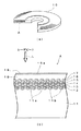
図1(a)は、本発明の好ましい実施態様にかかる光記録媒体10の外観を示す切り欠き斜視図であり、図1(b)は、図1(a)に示すA部を拡大した部分断面図である。
【0028】
図1(a),(b)に示す光記録媒体10は、外径が約120mm、厚みが約1.2mmである円盤状の光記録媒体であり、図1(b)に示すように、支持基板11と、防湿層12と、反射層13と、第2誘電体層14と、記録層15と、第1誘電体層16と、放熱層17と、光透過層18と、ハードコート層19を備えて構成されている。特に限定されるものではないが、本実施態様にかかる光記録媒体10は、波長λが380nm〜450nm、好ましくは約405nmであるレーザビームLをハードコート層19の表面である光入射面19aより照射することによってデータの記録及び再生を行うことが可能な書き換え型の光記録媒体である。光記録媒体10に対するデータの記録及び再生においては、開口数が0.7以上、好ましくは0.85程度の対物レンズが用いられ、これによって、レーザビームLの波長をλ、対物レンズの開口数をNAとした場合、λ/NA≦640nmに設定される。
【0029】
支持基板11は、光記録媒体10に求められる厚み(約1.2mm)を確保するために用いられる厚さ約1.1mmの円盤状の基板であり、その一方の面には、その中心部近傍から外縁部に向けて、レーザビームLをガイドするためのグルーブ11a及びランド11bが螺旋状に形成されている。特に限定されるものではないが、グルーブ11aの深さとしては10nm〜40nmに設定することが好ましく、グルーブ11aのピッチとしては0.2μm〜0.4μmに設定することが好ましい。支持基板11の材料としては種々の材料を用いることが可能であり、例えば、ガラス、セラミックス、あるいは樹脂を用いることができる。これらのうち、成形の容易性の観点から樹脂が好ましい。このような樹脂としてはポリカーボネート樹脂、オレフィン樹脂、アクリル樹脂、エポキシ樹脂、ポリスチレン樹脂、ポリエチレン樹脂、ポリプロピレン樹脂、シリコーン樹脂、フッ素系樹脂、ABS樹脂、ウレタン樹脂等が挙げられる。中でも、加工性などの点からポリカーボネート樹脂やオレフィン樹脂が特に好ましい。但し、支持基板11は、レーザビームLの光路とはならないことから、高い光透過性を有している必要はない。
【0030】
支持基板11の作製は、スタンパを用いた射出成形法を用いることが好ましいが、2P法等、他の方法によってこれを作製することも可能である。
【0031】
防湿層12は、その表面に設けられる反射層13の腐食防止を目的として設けられる層であり、誘電体によって構成される。防湿層12を構成する誘電体としては、Al2O3、AlN、ZnO、ZnS、GeN、GeCrN、CeO2、SiO、SiO2、Si3N4、SiC、La2O3、TaO、TiO2、SiAlON(SiO2,Al2O3,Si3N4及びAlNの混合物)及びLaSiON(La2O3,SiO2及びSi3N4の混合物)等、アルミニウム(Al)、シリコン(Si)、セリウム(Ce)、チタン(Ti)、亜鉛(Zn)、タンタル(Ta)等の酸化物、窒化物、硫化物、炭化物あるいはそれらの混合物を用いることが好ましく、腐食防止効果及び成膜速度を考慮すれば、ZnSとSiO2との混合物を用いることが特に好ましく、この場合、ZnSとSiO2のモル比を約80:20に設定することが最も好ましい。防湿層12は、複数の誘電体層からなる多層構造であっても構わない。
【0032】
また、防湿層12の層厚は特に限定されないが、50〜150nmに設定することが好ましい。防湿層12の層厚が50nm未満であると腐食防止効果が不十分となる一方、150nmを超えると成膜時間が長くなり生産性が低下するおそれがあるからである。
【0033】
尚、本発明において光記録媒体に防湿層12を設けることは必須でなく、これを省略しても構わない。
【0034】
反射層13は、ハードコート層19側から入射されるレーザビームLを反射し、再びハードコート層19から出射させる役割を果たすとともに、記録層14から見て支持基板11側における放熱層としての役割を果たし、さらに、多重干渉効果により再生信号(C/N比)を高める役割を果たす。本発明では、反射層13の材料としては銀(Ag)を主成分とし、これに副成分として少なくともネオジム(Nd)及び銅(Cu)が添加された合金が用いられる。この場合、主成分である銀(Ag)の比率は95atm%以上である必要があり、98atm%程度であることが好ましい。また、副成分であるネオジム(Nd)と銅(Cu)の原子比としては30:70〜70:30であることが好ましく、50:50程度であることがより好ましい。したがって、反射層13の材料としては、銀(Ag)、ネオジム(Nd)及び銅(Cu)の原子比が98:1:1程度であることが好ましく、98.4:0.7:0.9程度であることが最も好ましい。尚、本明細書においては、銀(Ag)を主成分とし(95atm%以上)、これに少なくともネオジム(Nd)及び銅(Cu)が添加された合金を「ANC合金」と呼ぶことがある。
【0035】
本発明において反射層13の材料としてANC合金を用いているのは次の理由による。すなわち、反射層の材料として従来より知られている銀(Ag)を主成分としこれにパラジウム(Pd)及び銅(Cu)が添加された合金(以下、「APC合金」という)は、高い熱伝導性と高い信頼性を併せ持つことから、高速記録が可能な書き換え型光記録媒体用の反射層の材料として好適であるが、記録層を構成する相変化材料の熱伝導性や結晶化速度等によっては反射層による放熱性が過剰となることがあり、この場合には記録感度が低下するという問題が発生する。これに対しANC合金は、APC合金と同等の信頼性を備えつつAPC合金よりもやや熱伝導性が低いという特性を有しており、このため、反射層13の材料としてANC合金を用いれば、高い信頼性を確保しつつ、放熱性が過剰となることがなくなる。その結果、記録感度を高めることが可能となる。
【0036】
また、本発明において反射層13の厚さは、60〜150nmに設定する必要があり、90〜110nmに設定することが好ましく、100nm程度に設定することが特に好ましい。これは、反射層13の厚さが60nm未満であると反射層13による上記効果を十分に得ることができない一方、反射層13の厚さが150nm超であると、放熱性が過剰となり記録感度が低下してしまうからであり、反射層13の厚さを90〜110nm、特に100nm程度に設定すれば、反射層13による上記効果を十分に得ることができるとともに、記録層14に対して最適な放熱性を与えることが可能となる。
【0037】
記録層15は可逆的な記録マークが形成される層であり、相変化材料によって構成される。相変化材料は、結晶状態である場合の反射率とアモルファス状態である場合の反射率とが異なるため、これを利用してデータの記録が行われる。記録されるデータは、例えばアモルファス状態である記録マークの長さ(記録マークの前縁から後縁までの長さ)及び例えば結晶状態であるブランク領域の長さ(記録マークの後縁から次の記録マークの前縁までの長さ)によって表現される。記録マーク及びブランク領域の長さは、基準となるクロックの1周期に相当する長さをTとした場合、Tの整数倍に設定され、具体的には、1,7RLL変調方式においては、2T〜8Tの長さを持つ記録マーク及びブランク領域が使用される。
【0038】
記録層15を結晶状態からアモルファス状態に変化させるためには、光入射面19aから照射されるレーザビームLを記録パワーPwから基底パワーPbまでの振幅を有するパルス波形とすることによって記録層15を融点以上の温度に加熱し、その後、レーザビームLのパワーを基底パワーPbに設定することによって急冷する。これによって溶融した領域がアモルファス状態に変化し、これが記録マークとなる。一方、記録層15をアモルファス状態から結晶状態に変化させるためには、光入射面19aから照射されるレーザビームLのパワーを消去パワーPeに設定することによって記録層15を結晶化温度以上の温度に加熱する。結晶化温度以上の温度に加熱された領域は、レーザビームLが遠ざかることによって徐冷されることから、当該領域が結晶状態に変化する。
【0039】
ここで、記録パワーPw、消去パワーPe及び基底パワーPbの関係は、
Pw>Pe≧Pb
に設定される。したがって、レーザビームLのパワーをこのように変調すれば、記録層15の未記録領域に記録マークを形成するだけでなく、既に記録マークが形成されている領域にこれと異なる記録マークを直接上書き(ダイレクトオーバーライト)することが可能となる。
【0040】
記録層15を構成する相変化材料の種類としては特に限定されるものではないが、高速でダイレクトオーバーライトを可能とするためには、アモルファス状態から結晶状態への構造変化に要する時間(結晶化時間)が短い材料を選択することが好ましく、このような材料としてはSbTe系材料を挙げることができる。SbTe系材料としてはSbTeのみでもよいし、結晶化時間をより短縮するとともに長期の保存に対する信頼性を高めるために添加物を加えてもよい。
【0041】
具体的には、記録層15を構成する相変化材料の原子比を
(SbxTe1−x)1−yMy M:Sb及びTeを除く元素
で表したとき、
0.55≦x≦0.9
0≦y≦0.25
であることが好ましく、
0.65≦x≦0.85
0≦y≦0.25
であることがより好ましい。
【0042】
元素Mの種類は特に限定されないが、短結晶化時間及び保存信頼性の観点から、インジウム(In),銀(Ag),金(Au),ビスマス(Bi),セレン(Se),アルミニウム(Al),リン(P),ゲルマニウム(Ge),水素(H),シリコン(Si),炭素(C),バナジウム(V),タングステン(W),タンタル(Ta),亜鉛(Zn),マンガン(Mn),チタン(Ti),錫(Sn),パラジウム(Pd),鉛(Pb),窒素(N),酸素(O)及び希土類元素からなる群より1又は2以上の元素を選択することが好ましい。特に、保存信頼性の観点からは、銀(Ag),インジウム(In),ゲルマニウム(Ge)及び希土類元素からなる群より1又は2以上の元素を選択することが好ましい。
【0043】
記録層15の層厚は、厚くなればなるほどレーザビームLのビームスポットが照射される記録層15の表面の平坦性が悪化し、これに伴って再生信号のノイズレベルが高くなるとともに、記録感度も低下する。この点を考慮すれば、記録層15の表面の平坦性を高めることによって再生信号のノイズレベルを抑制するとともに記録感度を高めるためには、記録層15の層厚を薄く設定することが有効であるが、薄くしすぎると記録前後における光学定数の差が少なくなり、再生時に高いレベルの再生信号(C/N比)を得ることができなくなる。また、記録層15の層厚を極端に薄く設定すると、成膜時における層厚制御が困難となる。以上を考慮すれば、記録層15の層厚としては2〜40nmに設定することが好ましく、4〜20nmに設定することがより好ましく、12nm程度に設定することがさらに好ましい。
【0044】
放熱層17、第1誘電体層16及び第2誘電体層14は、記録層15を物理的及び/又は化学的に保護する役割を果たし、記録層15は第1誘電体層16及び第2誘電体層14に挟持されることによって、光記録後、長期間にわたって記録情報の劣化が効果的に防止される。また、放熱層17、第1誘電体層16及び第2誘電体層14は、記録の前後における光学特性の差を拡大する役割をも果たし、さらに、放熱層17は、記録層15に生じている熱を速やかに放熱するための放熱層としての役割をも果たす。
【0045】
本発明では、第2誘電体層14を構成する材料としてZnSとSiO2との混合物が用いられ、ZnSとSiO2のモル比は40:60〜60:40に設定される。上記材料は記録層14に対する物理的な保護特性が優れているとともに、熱伝導性が比較的低いという特徴を有しており、このため第2誘電体層14の材料として上記材料を用いれば、記録による熱変形が効果的に防止されるため繰り返しのオーバーライトに対する高い信頼性が確保されるとともに、記録感度を高めることが可能となる。このような効果を最も顕著に得るためには、ZnSとSiO2のモル比を50:50程度に設定すればよい。また、ZnSとSiO2の混合物は成膜スピードが速いことから、生産性を高めることも可能となる。
【0046】
また、本発明において第2誘電体層14の厚さは、5〜20nmに設定する必要があり、10〜15nmに設定することが好ましく、12nm程度に設定することが特に好ましい。これは、第2誘電体層14の厚さが5nm未満であると記録層14を十分に保護できないおそれが生じる一方、上記材料は比較的膜応力が強いことから、第2誘電体層14の厚さが20nm超であるとクラックが発生するおそれがあるとともに、放熱性が低下しすぎるからであり、第2誘電体層14の厚さを10〜15nm、特に12nm程度に設定すれば、クラックの発生を防止しつつ高い信頼性を確保することができ、さらに、記録層14に対して最適な放熱性を与えることが可能となる。
【0047】
一方、第1誘電体層16を構成する材料は、使用されるレーザビームLの波長領域において透明な誘電体であれば特に限定されず、例えば、酸化物、硫化物、窒化物又はこれらの組み合わせを主成分として用いることができるが、記録による熱変形の防止、並びに、記録層15に対する保護特性の観点から、ZnO、ZnS、GeN、GeCrN、CeO2、SiO、SiO2、Si3N4、La2O3、TaO、TiO2、SiAlON(SiO2,Al2O3,Si3N4及びAlNの混合物)及びLaSiON(La2O3,SiO2及びSi3N4の混合物)等、アルミニウム(Al)、シリコン(Si)、セリウム(Ce)、チタン(Ti)、亜鉛(Zn)、タンタル(Ta)等の酸化物、窒化物、硫化物、炭化物あるいはそれらの混合物を用いることが好ましく、成膜スピードや光学特性を考慮すれば、ZnSとSiO2との混合物を用いることが特に好ましい。
【0048】
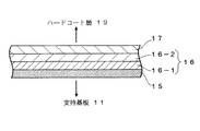
また、第1誘電体層16については、図2に示すように、相対的に物理特性に優れた材料からなる界面層16−1及び相対的に光学特性に優れた材料からなるエンハンス層16−2の2層構造とすることが特に好ましい。このように第1誘電体層16を2層構造とし、相対的に物理特性に優れる界面層16−1を記録層15側に配置し、相対的に光学特性に優れるエンハンス層16−2を放熱層17側に配置すれば、繰り返しのオーバーライトに対する高い信頼性を確保しつつ、良好な光学特性を得ることが可能となる。
【0049】
界面層16−1及びエンハンス層16−2の材料としては、いずれもZnSとSiO2との混合物を用い、界面層16−1よりもエンハンス層16−2の方がZnSの比率が大きく、エンハンス層16−2よりも界面層16−1の方がSiO2の比率が大きくなるよう、その組成比を設定することが好ましい。具体的には、界面層16−1についてはZnSとSiO2のモル比を40:60〜60:40、好ましくは50:50程度に設定し、エンハンス層16−2についてはZnSとSiO2のモル比を70:30〜90:10、好ましくは80:20程度に設定すればよい。このような組成比に設定すれば、上述の通り、繰り返しのオーバーライトに対する高い信頼性を確保しつつ良好な光学特性を得ることが可能となるばかりでなく、ZnSとSiO2の混合物は成膜スピードが速いことから、生産性を高めることも可能となる。
【0050】
第1誘電体層16の層厚は特に限定されないが、10〜50nmに設定することが好ましく、30nm程度とすることが特に好ましい。これは、第1誘電体層16の層厚が10nm未満であると記録層15の保護効果及び光学特性を拡大する効果が十分に得られなくなる一方、50nmを超えると成膜時間が長くなり生産性が低下するおそれがあるとともに、第1誘電体層16のもつ応力によってクラックが発生するおそれがあるからであり、また、第1誘電体層16の層厚を50nm超に設定すると、放熱層17による放熱効果が低下するからである。第1誘電体層16の層厚を10〜50nm、特に30nm程度に設定すれば、生産性の低下やクラックの発生を防止し、放熱効果を確保しつつ、上記効果を十分に得ることが可能となる。
【0051】
また、図2に示すように第1誘電体層16を界面層16−1及びエンハンス層16−2の2層構造とする場合には、界面層16−1よりもエンハンス層16−2の方が層厚が大きくなるように設定することが好ましい。より具体的には、界面層16−1の材料としてモル比が50:50であるZnSとSiO2の混合物を用い、エンハンス層16−2の材料としてモル比が80:20であるZnSとSiO2の混合物を用いる場合には、界面層16−1の層厚を1〜10nmに設定し、エンハンス層16−2の層厚を10〜40nmに設定することが好ましく、界面層16−1の層厚を5nm程度に設定し、エンハンス層16−2の層厚を25nm程度に設定することが非常に好ましい。これは、モル比が50:50であるZnSとSiO2の混合物は比較的応力が強く、また熱伝導性が比較的低いことから、本材料からなる界面層16−1の層厚を大きくしすぎると、クラックが生じ易くなるばかりでなく、放熱層17による放熱効果が低下するからである。
【0052】
さらに、放熱層17を構成する材料は、使用されるレーザビームLの波長領域において透明であり、且つ、第1誘電体層16を構成する材料よりも熱伝導性の高い誘電体であれば特に限定されず、第1誘電体層16と同様、アルミニウム(Al)、シリコン(Si)、セリウム(Ce)、チタン(Ti)、亜鉛(Zn)、タンタル(Ta)等の酸化物、窒化物、硫化物、炭化物あるいはそれらの混合物を用いることが可能であるが、第1誘電体層16の材料としてZnSとSiO2との混合物を用いる場合には、Al2O3を用いることが特に好ましい。Al2O3はZnSとSiO2との混合物に比べて熱伝導性が高く、これを放熱層17の材料として用いることにより記録層15からみて光入射面19a側における放熱性が効果的に高められる。これにより、クロストークが低減するとともに、再生によって記録データが劣化するいわゆる再生劣化現象が効果的に防止される。
【0053】
放熱層17の層厚は特に限定されないが、その材料としてAl2O3を用いる場合には15〜40nmに設定することが好ましく、30nm程度に設定することが特に好ましい。これは、Al2O3からなる放熱層17の層厚が15nm未満であると十分な放熱効果が得られなくなる一方、40nmを超えると成膜時間が長くなり生産性が低下するおそれがあるとともに、放熱層17のもつ応力によってクラックが発生するおそれがあるからである。放熱層17の層厚を15〜40nm、特に30nm程度に設定すれば、生産性の低下やクラックの発生を防止しつつ、記録層15に良好な放熱特性を与えることが可能となる。
【0054】
尚、上記防湿層12、反射層13、第2誘電体層14、記録層15、第1誘電体層16及び放熱層17の形成方法としては、これらの構成元素を含む化学種を用いた気相成長法、例えば、スパッタリング法や真空蒸着法を用いることができ、中でも、スパッタリング法を用いることが好ましい。
【0055】
光透過層18は、レーザビームLの光路となる層であり、その厚さとしては10〜300μmに設定することが好ましく、50〜150μmに設定することが特に好ましい。光透過層18の材料としては、使用されるレーザビームLの波長領域において光透過率が十分に高い材料である限り特に限定されないが、アクリル系又はエポキシ系の紫外線硬化性樹脂を用い、スピンコート法によってこれを放熱層17上に形成することが好ましい。また、紫外線硬化性樹脂を硬化させてなる膜のかわりに、光透過性樹脂からなる光透過性シートと各種接着剤や粘着剤を用いて光透過層18を形成してもよい。
【0056】
ハードコート層19は、光透過層18の表面を保護し、これによって光入射面19aに傷が生じるのを防止する役割を果たす。ハードコート層19の材料としては、光透過層18の材料よりも傷のつきにくい硬い材料であれば特に限定されず、例えば、エポキシアクリレートオリゴマー(2官能オリゴマー)、多官能アクリルモノマー、単官能アクリルモノマー及び光重合開始剤を含む紫外線硬化性樹脂や、アルミニウム(Al)、シリコン(Si)、セリウム(Ce)、チタン(Ti)、亜鉛(Zn)、タンタル(Ta)等の酸化物、窒化物、硫化物、炭化物あるいはそれらの混合物を用いることができる。ハードコート層19の材料として紫外線硬化性樹脂を用いる場合には、スピンコート法によってこれを光透過層18上に形成することが好ましく、上記酸化物、窒化物、硫化物、炭化物あるいはそれらの混合物を用いる場合には、これらの構成元素を含む化学種を用いた気相成長法、例えば、スパッタリング法や真空蒸着法を用いることができ、中でも、スパッタリング法を用いることが好ましい。
【0057】
また、ハードコート層19は、光入射面19aに傷が生じるのを防止する役割を果たすものであることから、硬いだけでなく、潤滑性を有していることが好ましい。ハードコート層19に潤滑性を与えるためには、ハードコート層19の母体となる材料(例えば、SiO2)に潤滑剤を含有させることが有効であり、潤滑剤としては、シリコーン系潤滑剤やフッ素系潤滑剤、脂肪酸エステル系潤滑剤を選択することが好ましく、その含有量としては、0.1〜5.0質量%程度とすることが好ましい。
【0058】
ハードコート層19の層厚は、光透過層18の表面を保護可能である限り、特に限定されない。尚、本発明において光記録媒体にハードコート層19を設けることは必須でなく、これを省略しても構わない。
【0059】
以上が本発明の好ましい実施態様にかかる光記録媒体10の構造である。
【0060】
このような構造を有する光記録媒体10に対してデータを記録する場合、上述の通り、光入射面19aから強度変調されたレーザビームLを照射し、記録層15の温度を融点以上の温度に加熱した後、急冷すれば当該領域はアモルファス状態となり、記録層15の温度を結晶化温度以上の温度に加熱した後、徐冷すれば当該領域は結晶状態となる。記録層15のうち、アモルファス状態となった部分(記録マークに相当)の反射率は、結晶状態となった部分(ブランク領域に相当)の反射率と異なった値となることから、これを利用してデータの記録・再生を行うことが可能となる。
【0061】
そして、本実施態様にかかる光記録媒体10においては、反射層13が厚さ60〜150nmのANC合金からなり、さらに、反射層13と記録層15との間に設けられる第2誘電体層14が厚さ5〜20nmであるZnSとSiO2との混合物(モル比=40:60〜60:40)からなることから、高い信頼性を確保しつつ、最適な放熱特性によって高い記録感度を得ることが可能となる。しかも、本実施態様においては。第1誘電体層16と光透過層18との間に放熱層17が設けられており、記録層15から見て反射層13とは反対側の放熱性が改善されていることから、広いパワーマージンを得ることが可能となるばかりでなく、クロストークが低減しさらに再生劣化現象が効果的に防止される。
【0062】
さらに、第1誘電体層16をを2層構造とし、相対的に物理特性に優れる界面層16−1を記録層15側に配置し、相対的に光学特性に優れるエンハンス層16−2を放熱層17側に配置すれば、記録層15に対する高い保護特性を確保しつつ、良好な光学特性を得ることが可能となる。
【0063】
以上より、本実施態様にかかる光記録媒体10によれば、必要な光学特性を満足し、且つ、記録層15に対する十分な保護特性を満足しつつ、記録感度とパワーマージンを両立させることが可能となる。すなわち、高速記録に適した書き換え型の光記録媒体を提供することが可能となる。
【0064】
本発明は、以上の実施態様に限定されることなく、特許請求の範囲に記載された発明の範囲内で種々の変更が可能であり、それらも本発明の範囲内に包含されるものであることはいうまでもない。
【0065】
【実施例】
以下、実施例を用いて本発明について更に具体的に説明するが、本発明はこれらの実施例に何ら限定されるものではない。
【0066】
[サンプルの作製]
以下の方法により、図1及び図2に示す構造と同じ構造を有する実施例による光記録媒体サンプルと比較例による光記録媒体サンプルを作製した。
【0067】
まず、射出成型法により、厚さ1.1mm、直径120mmであり、表面にグルーブ11a及びランド11b(トラックピッチ(グルーブのピッチ)=0.32μm、グルーブ11aの深さ=25nm)が形成されたポリカーボネートからなるディスク状の支持基板11を作製した。
【0068】
次に、この支持基板11をスパッタリング装置にセットし、グルーブ11a及びランド11bが形成されている側の表面にZnSとSiO2の混合物(モル比=80:20)からなる厚さ100nmの防湿層12、ANC合金(原子比=98.4:0.7:0.9)からなる厚さ100nmの反射層13、ZnSとSiO2の混合物(モル比=50:50)からなる厚さ12nmの第2誘電体層14、SbTeGeAg(原子比=74:20:5:1)からなる厚さ12nmの記録層15、ZnSとSiO2の混合物(モル比=50:50)からなる厚さ5nmの界面層16−1、ZnSとSiO2の混合物(モル比=80:20)からなる厚さ25nmのエンハンス層16−2、Al2O3からなる厚さ30nmの放熱層17を順次スパッタ法により形成した。
【0069】
次に、放熱層17上に、アクリル系紫外線硬化性樹脂をスピンコート法によりコーティングし、これに紫外線を照射して厚さ100μmの光透過層18を形成した。
【0070】
そして、防湿層12〜光透過層18が形成された支持基板11を再びスパッタリング装置にセットし、光透過層18の表面にSiO2を母体とし、これにシリコーン系潤滑剤が添加された厚さ1〜2μmのハードコート層19を形成した。
【0071】
これにより、実施例による光記録媒体サンプルが完成した。
【0072】
次に、反射層13を厚さ100nmのAPC合金(原子比=98.4:0.7:0.9)によって構成し、第2誘電体層14を厚さ12nmのCeO2とAl2O3の混合物(モル比=80:20)によって構成し、エンハンス層16−2の厚さを35nmに設定した他は、実施例による光記録媒体サンプルと同様にして比較例1による光記録媒体サンプルを作製した。
【0073】
さらに、第2誘電体層14を厚さ12nmのCeO2とAl2O3の混合物(モル比=80:20)によって構成し、エンハンス層16−2の厚さを30nmに設定した他は、実施例による光記録媒体サンプルと同様にして比較例2による光記録媒体サンプルを作製した。
【0074】
[サンプルの評価]
次に、各光記録媒体サンプルを光ディスク評価装置(商品名:DDU1000、パルステック社製)にセットし、5.3m/secの線速度で回転させながら、開口数が0.85である対物レンズを介して波長が405nmであるレーザビームを光入射面19aから記録層15に照射し、種々の記録パワーPwを用いて1,7RLL変調方式における2T信号〜8T信号からなる混合信号をそれぞれ記録した。この場合、フォーマット効率を約80%とした場合のデータ転送レートは、約36Mbpsである。尚、消去パワーPeについてはPe/Pw=0.68となるように設定し、基底パワーPbは0.1mWに固定した。
【0075】
そして、各光記録媒体サンプルに記録された混合信号を再生し、得られた再生信号のジッタを測定した。ここでいうジッタとはクロックジッタを指し、タイムインターバルアナライザにより再生信号の「ゆらぎ(σ)」を求め、σ/Tw(Tw:クロックの1周期)により算出した。尚、再生パワーPrは0.35mWに設定した。
【0076】
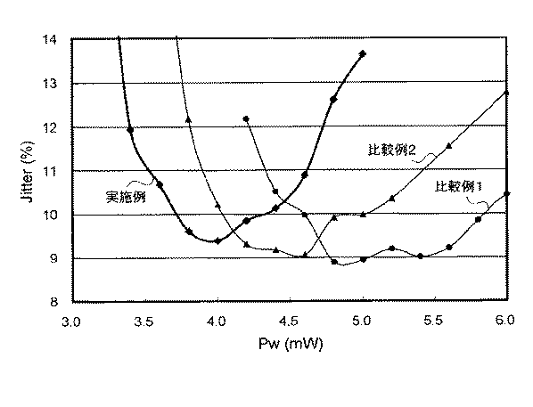
測定の結果を図3に示す。図3においては、両隣のトラックが記録状態である場合のジッタ(クロスジッタ)が示されている。クロスジッタの測定は、所定のトラックに混合信号を記録し、さらに両隣のトラックに混合信号を10回オーバーライトした後、上記所定のトラックに記録されたジッタを測定することにより行った。
【0077】
図3に示すように、比較例1,2の光記録媒体サンプルに比べ、実施例による光記録媒体サンプルの方がジッタが最低値(ボトム)となる記録パワーPwのレベルが低かった。すなわち記録感度が高かった。これは、比較例1による光記録媒体サンプルでは、反射層13がANC合金よりも熱伝導性の高いAPC合金からなるため記録層15からみて支持基板11側における放熱性が過剰となり、比較例2による光記録媒体サンプルでは、第2誘電体層14がZnSとSiO2の混合物(モル比=50:50)よりも熱伝導性の高いCeO2とAl2O3の混合物(モル比=80:20)からなるためやはり記録層15からみて支持基板11側における放熱性が過剰となったのに対し、実施例による光記録媒体サンプルでは、放熱性が過剰とならず、その結果、記録感度が高められたものと考えられる。
【0078】
【発明の効果】
以上説明したように、本発明においては、相変化材料からなる記録層の放熱性が最適化されていることから、高い信頼性を確保しつつ、高い記録感度と広いパワーマージンを確保することが可能となる。
【図面の簡単な説明】
【図1】(a)は、本発明の好ましい実施態様にかかる光記録媒体10の外観を示す切り欠き斜視図であり、(b)は(a)に示すA部を拡大した部分断面図である。
【図2】第1誘電体層16の好ましい構造を概略的に示す部分断面図である。
【図3】サンプルの評価における測定結果を示すグラフである。
【符号の説明】
10 光記録媒体
11 支持基板
11a グルーブ
11b ランド
12 防湿層
13 反射層
14 第2誘電体層
15 記録層
16 第1誘電体層
16−1 界面層
16−2 エンハンス層
17 放熱層
18 光透過層
19 ハードコート層
19a 光入射面
L レーザビーム[0001]
TECHNICAL FIELD OF THE INVENTION
The present invention relates to an optical recording medium, and more particularly to a rewritable optical recording medium capable of high-speed recording.
[0002]
[Prior art]
Conventionally, optical recording media represented by CDs and DVDs have been widely used as recording media for recording digital data. These optical recording media include a type of optical recording medium (ROM type optical recording medium) in which data cannot be additionally written or rewritten, such as a CD-ROM or a DVD-ROM, and a type of data, such as a CD-R or a DVD-R. An optical recording medium of a type that allows additional recording but cannot rewrite data (write-once type optical recording medium), and an optical recording medium of a type capable of rewriting data such as a CD-RW or DVD-RW (a rewritable optical recording medium) ).
[0003]
In a ROM type optical recording medium, data is generally recorded by a pit row formed on a substrate in advance at the time of manufacturing. In a write-once type optical recording medium, for example, a cyanine dye is used as a material of a recording layer. , Organic dyes such as phthalocyanine dyes and azo dyes are used, and data is obtained by utilizing changes in optical properties based on chemical changes (in some cases, physical changes may occur in addition to chemical changes). It is common to be recorded.
[0004]
On the other hand, in a rewritable optical recording medium, for example, a phase change material is used as a material of a recording layer, and data is generally recorded using a change in optical characteristics based on a change in the phase state. It is. That is, the phase change material has a different reflectivity when it is in a crystalline state and a reflectivity when it is in an amorphous state, so that data can be recorded using this. For example, if an area where the recording layer is in an amorphous state is a “recording mark” and an area where the recording layer is in a crystalline state is “blank”, the length of the recording mark (from the leading edge to the trailing edge of the recording mark) ) And the length of the blank (the length from the trailing edge of the recording mark to the leading edge of the next recording mark).
[0005]
When forming a recording mark on the recording layer, the recording layer is heated to a temperature exceeding the melting point by setting the power of the laser beam applied to the recording layer to a sufficiently high level (recording power Pw). The recording layer may be rapidly cooled by changing the power to a sufficiently low level (base power Pb). Thereby, since the phase change material changes from the crystalline state to the amorphous state, a recording mark can be formed. On the other hand, when erasing a recording mark that has already been formed, the recording layer is set at a crystallization temperature by setting the power of the laser beam applied to the recording layer to a level lower than the recording power Pw and higher than the base power Pb (erasing power Pe). What is necessary is just to heat above and to cool slowly. As a result, the phase change material changes from an amorphous state to a crystalline state, so that the recording mark is erased.
[0006]
Therefore, by modulating the power of the laser beam to a plurality of levels including the recording power Pw, the erasing power Pe, and the base power Pb, not only recording marks are formed in unrecorded areas of the recording layer, but also recording marks are already formed. It is possible to directly overwrite (direct overwrite) a different recording mark on the area in which it has been written.
[0007]
On the other hand, in recent years, next-generation optical recording media capable of increasing the data recording density and realizing a very high data transfer rate have been proposed. In such a next-generation optical recording medium, in order to realize a large capacity and a high data transfer rate, the beam spot diameter of a laser beam used for recording and reproducing data must be reduced to a very small size. . Here, in order to narrow the beam spot diameter, the numerical aperture (NA) of the objective lens for focusing the laser beam is increased to 0.7 or more, for example, to about 0.85, and the wavelength λ of the laser beam is increased. Needs to be reduced to 380 nm to 450 nm, for example, about 400 nm.
[0008]
However, when the NA of the objective lens for focusing the laser beam is increased, a problem arises in that the allowance of the warp and tilt of the optical recording medium, that is, the tilt margin becomes extremely small. The tilt margin T can be expressed by the following equation, where λ is the wavelength of a laser beam used for recording / reproducing, and d is the thickness of a light transmitting layer (transparent substrate) serving as an optical path of the laser beam.
[0009]
(Equation 1)
[0010]
(Equation 2)
[0011]
For these reasons, in the next-generation optical recording medium, the thickness of the light transmitting layer (transparent substrate) is reduced to about 100 μm in order to suppress the occurrence of coma while securing a sufficient tilt margin. Is required. For this reason, in the next-generation optical recording medium, it is difficult to form a recording layer or the like on a light-transmitting layer (transparent substrate) as in an existing optical recording medium such as a CD or a DVD. A method of forming a thin resin layer as a light transmitting layer (transparent substrate) on the formed recording layer or the like by a spin coating method or the like has been studied. Therefore, in the production of next-generation optical recording media, unlike current optical recording media in which film formation is performed sequentially from the light incident surface side, film formation is performed sequentially from the side opposite to the light incident surface. Become.
[0012]
[Problems to be solved by the invention]
Since such a next-generation optical recording medium requires an extremely high data transfer rate as described above, it is necessary to enable this in a rewritable optical recording medium in which the recording layer is made of a phase-change material. In this case, it is necessary to form the recording layer using a phase change material having a high crystallization speed, and it is necessary to set the recording power Pw of the laser beam sufficiently high when recording data.
[0013]
Even in such a case, the recording layer is required to have high heat dissipation in order to rapidly cool the recording layer which has reached a temperature exceeding the melting point and to form a recording mark having a good shape.
[0014]
The heat dissipation of the recording layer can be adjusted by the material and thickness of the dielectric layer and the reflective layer provided in the vicinity, but the heat dissipation of the recording layer can be adjusted by setting the material and the thickness of the dielectric layer and the reflective layer. If the recording performance is excessive, the recording sensitivity is reduced, while if the heat radiation performance is insufficient, the power margin (the range of the recording power Pw where the jitter is equal to or less than a predetermined value) is reduced. Therefore, it is necessary to optimize the setting of the heat dissipation by the dielectric layer and the reflection layer in consideration of both the recording sensitivity and the power margin, and the setting of the material and the thickness of the dielectric layer and the reflection layer is not necessary. It is necessary to perform the process in a range that satisfies the necessary optical characteristics and a sufficient protection characteristic for the recording layer, that is, a range in which high reliability is secured.
[0015]
However, it is not easy to satisfy such a condition in a next-generation optical recording medium that requires a very high data transfer rate.
[0016]
Therefore, an object of the present invention is to optimize the heat dissipation of a recording layer made of a phase change material, thereby having high recording sensitivity and a wide power margin, and at the same time, ensuring high reliability and enabling high-speed recording of a rewritable type. It is to provide an optical recording medium.
[0017]
[Means for Solving the Problems]
An object of the present invention is to provide a recording layer made of a phase change material and capable of forming a recording mark by irradiating a laser beam, and a first layer provided on the laser beam incident surface side as viewed from the recording layer. A dielectric layer, a second dielectric layer provided on a side opposite to the laser beam incident surface as viewed from the recording layer, and a laser beam incident surface as viewed from the second dielectric layer. And a reflective layer provided on the opposite side. The reflective layer has a thickness of 80 to 120 nm containing silver (Ag) as a main component and at least neodymium (Nd) and copper (Cu) added thereto. And the second dielectric layer is made of ZnS and SiO 2 (Molar ratio = 40: 60 to 60:40) and a layer having a thickness of 8 to 20 nm.
[0018]
According to the present invention, a material having a slightly lower thermal conductivity than a material generally used as a material of the reflective layer and the second dielectric layer is selected, and furthermore, its thickness is optimized, The heat dissipation on the side opposite to the incident surface as viewed from the recording layer does not become excessive. This makes it possible to obtain high recording sensitivity while ensuring high reliability.
[0019]
In this case, the ratio of silver (Ag) as the main component of the reflective layer is preferably about 98 atm%, and the atomic ratio of neodymium (Nd) and copper (Cu) as the sub components is 30:70 to The ratio is preferably 70:30, and more preferably about 50:50. The thickness of the reflective layer is preferably from 90 to 110 nm, particularly preferably about 100 nm.
[0020]
Further, ZnS and SiO constituting the second dielectric layer 2 Is preferably about 50:50, and the layer thickness is preferably 5 to 20 nm, particularly preferably about 12 nm.
[0021]
Further, it is more preferable to further include a heat radiation layer provided on the laser beam incident surface side as viewed from the first dielectric layer. According to this, the heat radiation on the incident surface side as viewed from the recording layer is improved, so that not only a wide power margin can be obtained, but also crosstalk is reduced, and the reproduction deterioration phenomenon is effectively prevented. Is prevented.
[0022]
Further, the first dielectric layer is provided in contact with the recording layer, and is formed of ZnS and SiO. 2 ZnS and SiO 2 provided in contact with the interface layer mainly containing a mixture of 2 It is preferable that the enhanced layer has a higher ZnS ratio than the interface layer. ZnS and SiO 2 In a mixture of 2 When the ratio is increased, the physical characteristics are improved, and when the ratio of ZnS is increased, the optical characteristics are improved. Therefore, if the relationship between the composition ratio in the interface layer and the composition ratio in the enhanced layer is set in this manner, Good optical characteristics can be obtained while securing high protection characteristics. In this case, ZnS and SiO in the interface layer 2 Is about 50:50, and ZnS and SiO in the enhanced layer are 2 Is more preferably about 80:20.
[0023]
Further, it is preferable that the enhanced layer has a larger thickness than the interface layer. The interface layer is SiO 2 Because the ratio is high, the stress is relatively strong, and the thermal conductivity is relatively low.If the layer thickness is too large, not only cracks are likely to occur but also the heat radiation effect by the heat radiation layer is reduced. is there.
[0024]
Further, the recording layer is made of a SbTe-based material, and its composition is represented by a general formula
(Sb x Te 1-x ) 1-y M y (M is an element excluding Sb and Te)
When represented by
0.55 ≦ x ≦ 0.9, and
0 ≦ y ≦ 0.25
Is preferably satisfied. Since such a material has a high crystallization speed, data can be recorded at a high linear velocity. In this case, it is more preferable that the element represented by M in the above general formula contains germanium (Ge) and terbium (Tb). According to this, the crystallization speed is further increased, and data can be recorded at a higher linear velocity.
[0025]
A light transmitting layer provided on the incident surface side of the laser beam when viewed from the heat radiation layer and having a thickness of 10 to 300 μm, wherein the wavelength of the laser beam is λ, and the laser beam is focused. When the numerical aperture of the objective lens is NA, it is preferable that data can be recorded by setting λ / NA ≦ 640 nm. Such an optical recording medium is a so-called next-generation optical recording medium, and although a very high data transfer rate is required, according to the present invention, heat dissipation on the side opposite to the incident surface when viewed from the recording layer is reduced. Since there is no excess, it is possible to obtain high recording sensitivity while securing high reliability.
[0026]
BEST MODE FOR CARRYING OUT THE INVENTION
Hereinafter, preferred embodiments of the present invention will be described in detail with reference to the accompanying drawings.
[0027]
FIG. 1A is a cutaway perspective view showing an appearance of an optical recording medium 10 according to a preferred embodiment of the present invention, and FIG. 1B is an enlarged view of a portion A shown in FIG. It is sectional drawing.
[0028]
The optical recording medium 10 shown in FIGS. 1A and 1B is a disk-shaped optical recording medium having an outer diameter of about 120 mm and a thickness of about 1.2 mm. As shown in FIG. Support substrate 11, moisture-proof layer 12, reflection layer 13, second dielectric layer 14, recording layer 15, first dielectric layer 16, heat radiation layer 17, light transmission layer 18, hard coat layer 19 is provided. Although not particularly limited, the optical recording medium 10 according to the present embodiment emits a laser beam L having a wavelength λ of 380 nm to 450 nm, preferably about 405 nm from a light incident surface 19 a which is the surface of the hard coat layer 19. This is a rewritable optical recording medium capable of recording and reproducing data by irradiation. In recording and reproducing data on and from the optical recording medium 10, an objective lens having a numerical aperture of 0.7 or more, preferably about 0.85 is used, whereby the wavelength of the laser beam L is λ, the numerical aperture of the objective lens is Is set to λ / NA ≦ 640 nm.
[0029]
The support substrate 11 is a disk-shaped substrate having a thickness of about 1.1 mm used for securing a thickness (about 1.2 mm) required for the optical recording medium 10, and one surface thereof has a central portion. A groove 11a and a land 11b for guiding the laser beam L are spirally formed from the vicinity to the outer edge. Although not particularly limited, the depth of the groove 11a is preferably set to 10 nm to 40 nm, and the pitch of the groove 11a is preferably set to 0.2 μm to 0.4 μm. Various materials can be used as the material of the support substrate 11, and for example, glass, ceramics, or resin can be used. Of these, resins are preferred from the viewpoint of ease of molding. Examples of such a resin include a polycarbonate resin, an olefin resin, an acrylic resin, an epoxy resin, a polystyrene resin, a polyethylene resin, a polypropylene resin, a silicone resin, a fluorine-based resin, an ABS resin, and a urethane resin. Among them, a polycarbonate resin and an olefin resin are particularly preferable from the viewpoint of workability and the like. However, since the support substrate 11 does not serve as an optical path of the laser beam L, it is not necessary to have high light transmittance.
[0030]
The support substrate 11 is preferably manufactured by an injection molding method using a stamper, but may be manufactured by another method such as a 2P method.
[0031]
The moisture-proof layer 12 is a layer provided for the purpose of preventing corrosion of the reflective layer 13 provided on the surface thereof, and is made of a dielectric. The dielectric constituting the moisture-proof layer 12 is Al 2 O 3 , AlN, ZnO, ZnS, GeN, GeCrN, CeO 2 , SiO, SiO 2 , Si 3 N 4 , SiC, La 2 O 3 , TaO, TiO 2 , SiAlON (SiO 2 , Al 2 O 3 , Si 3 N 4 And AlN) and LaSiON (La 2 O 3 , SiO 2 And Si 3 N 4 ), Oxides such as aluminum (Al), silicon (Si), cerium (Ce), titanium (Ti), zinc (Zn), and tantalum (Ta), nitrides, sulfides, carbides, and mixtures thereof. It is preferable to use ZnS and SiOS in consideration of the corrosion prevention effect and the film formation rate. 2 It is particularly preferred to use a mixture of ZnS and SiO2. 2 Is most preferably set to about 80:20. The moisture-proof layer 12 may have a multilayer structure including a plurality of dielectric layers.
[0032]
The thickness of the moisture-proof layer 12 is not particularly limited, but is preferably set to 50 to 150 nm. If the thickness of the moisture-proof layer 12 is less than 50 nm, the effect of preventing corrosion will be insufficient, while if it exceeds 150 nm, the film formation time will be long and the productivity may be reduced.
[0033]
In the present invention, the provision of the moisture-proof layer 12 on the optical recording medium is not essential, and may be omitted.
[0034]
The reflection layer 13 reflects the laser beam L incident from the hard coat layer 19 side and emits the laser beam L again from the hard coat layer 19, and also functions as a heat radiation layer on the support substrate 11 side as viewed from the recording layer 14. And plays the role of enhancing the reproduction signal (C / N ratio) by the multiple interference effect. In the present invention, as a material of the reflective layer 13, an alloy containing silver (Ag) as a main component and at least neodymium (Nd) and copper (Cu) as subcomponents is used. In this case, the ratio of silver (Ag) as a main component needs to be 95 atm% or more, and preferably about 98 atm%. Further, the atomic ratio between neodymium (Nd) and copper (Cu), which are subcomponents, is preferably from 30:70 to 70:30, and more preferably about 50:50. Therefore, as a material of the reflective layer 13, the atomic ratio of silver (Ag), neodymium (Nd), and copper (Cu) is preferably about 98: 1: 1, and 98.4: 0.7: 0. Most preferably, it is about 9. In the present specification, an alloy containing silver (Ag) as a main component (95 atm% or more) and at least neodymium (Nd) and copper (Cu) added thereto may be referred to as an “ANC alloy”.
[0035]
In the present invention, the reason why the ANC alloy is used as the material of the reflection layer 13 is as follows. That is, an alloy containing silver (Ag) as a main component, which is conventionally known as a material of the reflective layer, and palladium (Pd) and copper (Cu) added thereto (hereinafter, referred to as “APC alloy”) has a high heat. Since it has both conductivity and high reliability, it is suitable as a material for a reflective layer for a rewritable optical recording medium capable of high-speed recording, but the thermal conductivity and crystallization speed of the phase-change material constituting the recording layer, etc. In some cases, the heat dissipation by the reflective layer may be excessive, and in this case, there is a problem that the recording sensitivity is reduced. On the other hand, the ANC alloy has a characteristic that the thermal conductivity is slightly lower than the APC alloy while having the same reliability as the APC alloy. Therefore, if the ANC alloy is used as the material of the reflective layer 13, While ensuring high reliability, the heat dissipation does not become excessive. As a result, it is possible to increase the recording sensitivity.
[0036]
In the present invention, the thickness of the reflection layer 13 needs to be set to 60 to 150 nm, preferably set to 90 to 110 nm, and particularly preferably set to about 100 nm. This is because if the thickness of the reflective layer 13 is less than 60 nm, the above-mentioned effect of the reflective layer 13 cannot be sufficiently obtained, while if the thickness of the reflective layer 13 exceeds 150 nm, the heat radiation property becomes excessive and the recording sensitivity becomes excessive. If the thickness of the reflective layer 13 is set to 90 to 110 nm, particularly about 100 nm, the above-described effect of the reflective layer 13 can be sufficiently obtained, and the recording layer 14 is optimal. It is possible to provide an excellent heat dissipation.
[0037]
The recording layer 15 is a layer on which reversible recording marks are formed, and is made of a phase change material. Since the reflectivity of the phase change material in a crystalline state is different from the reflectivity in an amorphous state, data recording is performed using this. The data to be recorded includes, for example, the length of a recording mark in an amorphous state (the length from the leading edge to the trailing edge of the recording mark) and the length of a blank area in a crystalline state (from the trailing edge of the recording mark to the next one). (Length to the leading edge of the recording mark). The length of the recording mark and the blank area is set to an integral multiple of T when the length corresponding to one cycle of the reference clock is T. Specifically, in the 1,7 RLL modulation method, 2T is used. Recording marks and blank areas with a length of ~ 8T are used.
[0038]
In order to change the recording layer 15 from the crystalline state to the amorphous state, the recording layer 15 is formed by changing the laser beam L emitted from the light incident surface 19a into a pulse waveform having an amplitude from the recording power Pw to the base power Pb. The laser beam is heated to a temperature equal to or higher than the melting point, and then rapidly cooled by setting the power of the laser beam L to the base power Pb. As a result, the melted area changes to an amorphous state, which becomes a recording mark. On the other hand, in order to change the recording layer 15 from the amorphous state to the crystalline state, the power of the laser beam L irradiated from the light incident surface 19a is set to the erasing power Pe so that the recording layer 15 is heated to a temperature higher than the crystallization temperature. Heat to The region heated to a temperature equal to or higher than the crystallization temperature is gradually cooled as the laser beam L moves away, so that the region changes to a crystalline state.
[0039]
Here, the relationship among the recording power Pw, the erasing power Pe, and the base power Pb is as follows.
Pw> Pe ≧ Pb
Is set to Therefore, by modulating the power of the laser beam L in this manner, not only a recording mark is formed in an unrecorded area of the recording layer 15 but also a different recording mark is directly overwritten on an area where a recording mark has been formed. (Direct overwrite).
[0040]
Although the type of the phase change material constituting the recording layer 15 is not particularly limited, in order to enable high-speed direct overwrite, the time required for a structural change from an amorphous state to a crystalline state (crystallization It is preferable to select a material having a short time), such as a SbTe-based material. As the SbTe-based material, only SbTe may be used, or an additive may be added in order to further shorten the crystallization time and increase the reliability for long-term storage.
[0041]
Specifically, the atomic ratio of the phase change material forming the recording layer 15 is
(Sb x Te 1-x ) 1-y M y M: Elements other than Sb and Te
When represented by
0.55 ≦ x ≦ 0.9
0 ≦ y ≦ 0.25
Is preferably
0.65 ≦ x ≦ 0.85
0 ≦ y ≦ 0.25
Is more preferable.
[0042]
The type of the element M is not particularly limited, but from the viewpoint of short crystallization time and storage reliability, indium (In), silver (Ag), gold (Au), bismuth (Bi), selenium (Se), and aluminum (Al) are used. ), Phosphorus (P), germanium (Ge), hydrogen (H), silicon (Si), carbon (C), vanadium (V), tungsten (W), tantalum (Ta), zinc (Zn), manganese (Mn) ), Titanium (Ti), tin (Sn), palladium (Pd), lead (Pb), nitrogen (N), oxygen (O) and one or more elements selected from the group consisting of rare earth elements. . In particular, from the viewpoint of storage reliability, it is preferable to select one or more elements from the group consisting of silver (Ag), indium (In), germanium (Ge), and rare earth elements.
[0043]
As the layer thickness of the recording layer 15 increases, the flatness of the surface of the recording layer 15 irradiated with the beam spot of the laser beam L deteriorates, and accordingly, the noise level of the reproduction signal increases and the recording sensitivity increases. Also decrease. Considering this point, it is effective to set the thickness of the recording layer 15 to be small in order to suppress the noise level of the reproduction signal and increase the recording sensitivity by increasing the flatness of the surface of the recording layer 15. However, if the thickness is too small, the difference between the optical constants before and after recording is reduced, and a high-level reproduction signal (C / N ratio) cannot be obtained during reproduction. Further, if the layer thickness of the recording layer 15 is set to be extremely thin, it becomes difficult to control the layer thickness during film formation. In consideration of the above, the layer thickness of the recording layer 15 is preferably set to 2 to 40 nm, more preferably 4 to 20 nm, and even more preferably about 12 nm.
[0044]
The heat radiation layer 17, the first dielectric layer 16 and the second dielectric layer 14 serve to physically and / or chemically protect the recording layer 15, and the recording layer 15 is composed of the first dielectric layer 16 and the second dielectric layer 16. By being sandwiched between the dielectric layers 14, deterioration of recorded information is effectively prevented for a long period after optical recording. Further, the heat dissipation layer 17, the first dielectric layer 16, and the second dielectric layer 14 also play a role in enlarging the difference in optical characteristics before and after recording. Further, the heat dissipation layer 17 is formed on the recording layer 15. It also serves as a heat dissipation layer to quickly dissipate the heat that is present.
[0045]
In the present invention, ZnS and SiO 2 are used as materials for forming the second dielectric layer 14. 2 And a mixture of ZnS and SiO 2 Is set in the range of 40:60 to 60:40. The material has excellent physical protection properties for the recording layer 14 and relatively low thermal conductivity. Therefore, if the material is used as the material of the second dielectric layer 14, Since thermal deformation due to recording is effectively prevented, high reliability against repeated overwriting is ensured, and recording sensitivity can be increased. In order to obtain such effects most remarkably, ZnS and SiO 2 May be set to about 50:50. ZnS and SiO 2 Since the mixture of (1) and (2) has a high film forming speed, the productivity can be improved.
[0046]
In the present invention, the thickness of the second dielectric layer 14 needs to be set to 5 to 20 nm, preferably set to 10 to 15 nm, and particularly preferably set to about 12 nm. If the thickness of the second dielectric layer 14 is less than 5 nm, the recording layer 14 may not be sufficiently protected. On the other hand, since the material has relatively high film stress, the second dielectric layer 14 If the thickness is more than 20 nm, cracks may occur, and the heat dissipation may be too low. If the thickness of the second dielectric layer 14 is set to 10 to 15 nm, particularly about 12 nm, cracks may occur. High reliability can be ensured while preventing the occurrence of the heat generation, and the recording layer 14 can be given optimal heat radiation.
[0047]
On the other hand, the material forming the first dielectric layer 16 is not particularly limited as long as it is a dielectric transparent in the wavelength region of the laser beam L to be used. For example, oxide, sulfide, nitride or a combination thereof is used. Can be used as a main component, but from the viewpoint of preventing thermal deformation due to recording and protecting properties for the recording layer 15, ZnO, ZnS, GeN, GeCrN, CeO 2 , SiO, SiO 2 , Si 3 N 4 , La 2 O 3 , TaO, TiO 2 , SiAlON (SiO 2 , Al 2 O 3 , Si 3 N 4 And AlN) and LaSiON (La 2 O 3 , SiO 2 And Si 3 N 4 ), Oxides such as aluminum (Al), silicon (Si), cerium (Ce), titanium (Ti), zinc (Zn), and tantalum (Ta), nitrides, sulfides, carbides, and mixtures thereof. It is preferable to use ZnS and SiOS in consideration of the film forming speed and the optical characteristics. 2 It is particularly preferred to use a mixture with
[0048]
As shown in FIG. 2, the first dielectric layer 16 has an interface layer 16-1 made of a material having relatively excellent physical properties and an enhancement layer 16- made of a material having relatively excellent optical properties. It is particularly preferred to have a two-layer structure of 2. As described above, the first dielectric layer 16 has a two-layer structure, the interface layer 16-1 having relatively excellent physical properties is disposed on the recording layer 15 side, and the enhancement layer 16-2 having relatively excellent optical properties is radiated. By arranging it on the layer 17 side, it is possible to obtain good optical characteristics while securing high reliability against repeated overwriting.
[0049]
As a material of the interface layer 16-1 and the enhance layer 16-2, ZnS and SiO 2 , The enhancement layer 16-2 has a higher ZnS ratio than the interface layer 16-1, and the interface layer 16-1 has a higher SiO2 ratio than the enhancement layer 16-2. 2 It is preferable to set the composition ratio so that the ratio becomes large. Specifically, for the interface layer 16-1, ZnS and SiO 2 Is set to about 40:60 to 60:40, preferably about 50:50, and ZnS and SiO 2 May be set to about 70:30 to 90:10, preferably about 80:20. By setting such a composition ratio, as described above, not only it is possible to obtain good optical characteristics while ensuring high reliability against repeated overwriting, but also ZnS and SiO 2 2 Since the mixture of (1) and (2) has a high film forming speed, the productivity can be improved.
[0050]
The layer thickness of the first dielectric layer 16 is not particularly limited, but is preferably set to 10 to 50 nm, and particularly preferably about 30 nm. This is because if the thickness of the first dielectric layer 16 is less than 10 nm, the protective effect of the recording layer 15 and the effect of expanding the optical characteristics cannot be sufficiently obtained. This is because there is a possibility that the property may be reduced and a crack may be generated due to the stress of the first dielectric layer 16. Further, if the thickness of the first dielectric layer 16 is set to more than 50 nm, the heat radiation layer This is because the heat radiation effect of the No. 17 decreases. If the layer thickness of the first dielectric layer 16 is set to 10 to 50 nm, particularly about 30 nm, it is possible to prevent the reduction in productivity and the occurrence of cracks, and to obtain the above-mentioned effects sufficiently while securing the heat radiation effect. It becomes.
[0051]
When the first dielectric layer 16 has a two-layer structure of the interface layer 16-1 and the enhance layer 16-2 as shown in FIG. 2, the enhance layer 16-2 has a larger thickness than the interface layer 16-1. Is preferably set so as to increase the layer thickness. More specifically, ZnS and SiO having a molar ratio of 50:50 are used as the material of the interface layer 16-1. 2 And a mixture of ZnS and SiO having a molar ratio of 80:20 as a material of the enhancement layer 16-2. 2 When using a mixture of, the layer thickness of the interface layer 16-1 is preferably set to 1 to 10 nm, and the layer thickness of the enhancement layer 16-2 is preferably set to 10 to 40 nm. It is highly preferable that the thickness is set to about 5 nm and the layer thickness of the enhancement layer 16-2 is set to about 25 nm. This is because ZnS and SiO at a molar ratio of 50:50 2 Is relatively high in stress and relatively low in thermal conductivity. Therefore, if the thickness of the interface layer 16-1 made of the present material is too large, not only cracks are easily generated but also the heat radiation layer 17-1. This is because the heat radiation effect due to this decreases.
[0052]
Further, the material constituting the heat radiation layer 17 is particularly a dielectric which is transparent in the wavelength region of the laser beam L to be used and has a higher thermal conductivity than the material constituting the first dielectric layer 16. There is no limitation, as with the first dielectric layer 16, oxides, nitrides, such as aluminum (Al), silicon (Si), cerium (Ce), titanium (Ti), zinc (Zn), and tantalum (Ta). It is possible to use sulfide, carbide or a mixture thereof, but ZnS and SiO 2 are used as the material of the first dielectric layer 16. 2 When using a mixture with 2 O 3 It is particularly preferred to use Al 2 O 3 Is ZnS and SiO 2 The heat conductivity is higher than that of the mixture of the above, and by using this as a material of the heat radiation layer 17, the heat radiation on the light incident surface 19a side as viewed from the recording layer 15 is effectively increased. This reduces crosstalk and effectively prevents a so-called reproduction degradation phenomenon in which recorded data is degraded by reproduction.
[0053]
The thickness of the heat radiation layer 17 is not particularly limited, 2 O 3 Is preferably set to 15 to 40 nm, and particularly preferably set to about 30 nm. This is Al 2 O 3 When the thickness of the heat radiation layer 17 is less than 15 nm, a sufficient heat radiation effect cannot be obtained. On the other hand, when the thickness exceeds 40 nm, the film formation time is prolonged and productivity may be reduced. This may cause cracks. When the thickness of the heat radiation layer 17 is set to 15 to 40 nm, particularly about 30 nm, it is possible to provide the recording layer 15 with good heat radiation characteristics while preventing a decrease in productivity and generation of cracks.
[0054]
The method for forming the moisture-proof layer 12, the reflective layer 13, the second dielectric layer 14, the recording layer 15, the first dielectric layer 16, and the heat radiation layer 17 is based on a method using chemical species containing these constituent elements. A phase growth method, for example, a sputtering method or a vacuum evaporation method can be used, and among them, a sputtering method is preferable.
[0055]
The light transmitting layer 18 is a layer that becomes an optical path of the laser beam L, and its thickness is preferably set to 10 to 300 μm, and particularly preferably set to 50 to 150 μm. The material of the light transmitting layer 18 is not particularly limited as long as the material has a sufficiently high light transmittance in the wavelength region of the laser beam L to be used, and an acrylic or epoxy ultraviolet curable resin is used. This is preferably formed on the heat radiation layer 17 by a method. Further, instead of the film formed by curing the ultraviolet curable resin, the light transmitting layer 18 may be formed by using a light transmitting sheet made of a light transmitting resin and various adhesives or adhesives.
[0056]
The hard coat layer 19 serves to protect the surface of the light transmitting layer 18 and thereby prevent the light incident surface 19a from being damaged. The material of the hard coat layer 19 is not particularly limited as long as it is a hard material that is less likely to be damaged than the material of the light transmission layer 18. For example, epoxy acrylate oligomer (bifunctional oligomer), polyfunctional acrylic monomer, monofunctional acrylic UV curable resin containing a monomer and a photopolymerization initiator, oxides such as aluminum (Al), silicon (Si), cerium (Ce), titanium (Ti), zinc (Zn), tantalum (Ta), and nitrides , Sulfide, carbide, or a mixture thereof. When an ultraviolet curable resin is used as the material of the hard coat layer 19, it is preferable to form the hard coat layer 19 on the light transmitting layer 18 by a spin coating method, and the above oxide, nitride, sulfide, carbide or a mixture thereof is used. Is used, a vapor phase growth method using a chemical species containing these constituent elements, for example, a sputtering method or a vacuum evaporation method can be used, and among them, the sputtering method is preferable.
[0057]
Further, since the hard coat layer 19 plays a role of preventing the light incidence surface 19a from being damaged, it is preferable that the hard coat layer 19 not only has a hard property but also has lubricity. In order to impart lubricity to the hard coat layer 19, a material (for example, SiO 2 It is effective to include a lubricant in (1), and as the lubricant, it is preferable to select a silicone-based lubricant, a fluorine-based lubricant, or a fatty acid ester-based lubricant. It is preferable to be about 5.0% by mass.
[0058]
The thickness of the hard coat layer 19 is not particularly limited as long as the surface of the light transmission layer 18 can be protected. In the present invention, the provision of the hard coat layer 19 on the optical recording medium is not essential, and may be omitted.
[0059]
The above is the structure of the optical recording medium 10 according to the preferred embodiment of the present invention.
[0060]
When data is recorded on the optical recording medium 10 having such a structure, as described above, the intensity-modulated laser beam L is irradiated from the light incident surface 19a to raise the temperature of the recording layer 15 to a temperature equal to or higher than the melting point. After heating, if rapidly cooled, the region becomes amorphous. If the temperature of the recording layer 15 is heated to a temperature equal to or higher than the crystallization temperature, and then gradually cooled, the region becomes crystalline. Since the reflectance of the amorphous portion (corresponding to the recording mark) of the recording layer 15 has a different value from the reflectance of the crystalline portion (corresponding to the blank area), this is utilized. Thus, data can be recorded and reproduced.
[0061]
In the optical recording medium 10 according to the present embodiment, the reflection layer 13 is made of an ANC alloy having a thickness of 60 to 150 nm, and further, the second dielectric layer 14 provided between the reflection layer 13 and the recording layer 15. And ZnS having a thickness of 5 to 20 nm 2 (Molar ratio = 40:60 to 60:40), it is possible to obtain high recording sensitivity with optimum heat radiation characteristics while ensuring high reliability. Moreover, in this embodiment. A heat dissipation layer 17 is provided between the first dielectric layer 16 and the light transmission layer 18, and the heat dissipation on the side opposite to the reflection layer 13 when viewed from the recording layer 15 is improved, so that a wide power Not only is it possible to obtain a margin, but also crosstalk is reduced and the reproduction deterioration phenomenon is effectively prevented.
[0062]
Further, the first dielectric layer 16 has a two-layer structure, the interface layer 16-1 having relatively excellent physical properties is disposed on the recording layer 15 side, and the enhancement layer 16-2 having relatively excellent optical properties is radiated. By arranging it on the layer 17 side, it is possible to obtain good optical characteristics while securing high protection characteristics for the recording layer 15.
[0063]
As described above, according to the optical recording medium 10 of the present embodiment, it is possible to achieve both the recording sensitivity and the power margin while satisfying the necessary optical characteristics and the sufficient protection characteristics for the recording layer 15. It becomes. That is, a rewritable optical recording medium suitable for high-speed recording can be provided.
[0064]
The present invention is not limited to the above embodiments, and various changes can be made within the scope of the invention described in the claims, and these are also included in the scope of the present invention. Needless to say.
[0065]
【Example】
Hereinafter, the present invention will be described more specifically with reference to examples, but the present invention is not limited to these examples.
[0066]
[Preparation of sample]
The optical recording medium sample according to the example and the optical recording medium sample according to the comparative example having the same structure as that shown in FIGS. 1 and 2 were manufactured by the following method.
[0067]
First, a groove 11a and a land 11b (track pitch (groove pitch) = 0.32 μm, groove 11a depth = 25 nm) were formed on the surface by injection molding with a thickness of 1.1 mm and a diameter of 120 mm. A disk-shaped support substrate 11 made of polycarbonate was produced.
[0068]
Next, this support substrate 11 is set in a sputtering apparatus, and ZnS and SiO 2 are formed on the surface on which the groove 11a and the land 11b are formed. 2 A 100 nm thick reflective layer 13 made of an ANC alloy (atomic ratio = 98.4: 0.7: 0.9), and a ZnS layer. SiO 2 12 nm thick second dielectric layer 14 made of a mixture (molar ratio = 50: 50), 12 nm thick recording layer 15 made of SbTeGeAg (atomic ratio = 74: 20: 5: 1), ZnS and SiO 2 Layer 16-1 of a mixture (molar ratio = 50: 50) of 5 nm in thickness, ZnS and SiO 2 Layer 16-2 of a mixture (molar ratio = 80: 20) having a thickness of 25 nm and Al 2 O 3 A heat radiation layer 17 having a thickness of 30 nm was formed by sputtering in order.
[0069]
Next, an acrylic ultraviolet curable resin was coated on the heat radiation layer 17 by a spin coating method, and this was irradiated with ultraviolet light to form a light transmitting layer 18 having a thickness of 100 μm.
[0070]
Then, the support substrate 11 on which the moisture-proof layer 12 to the light transmission layer 18 are formed is set again in the sputtering apparatus, and the surface of the light transmission layer 18 is coated with SiO 2. 2 And a silicone-based lubricant was added thereto to form a hard coat layer 19 having a thickness of 1 to 2 μm.
[0071]
Thus, the optical recording medium sample according to the example was completed.
[0072]
Next, the reflection layer 13 is made of an APC alloy having a thickness of 100 nm (atomic ratio = 98.4: 0.7: 0.9), and the second dielectric layer 14 is made of CeO having a thickness of 12 nm. 2 And Al 2 O 3 (Mole ratio = 80: 20) and the thickness of the enhancement layer 16-2 was set to 35 nm, except that the optical recording medium sample of Comparative Example 1 was the same as the optical recording medium sample of Example. Produced.
[0073]
Further, the second dielectric layer 14 is made of CeO having a thickness of 12 nm. 2 And Al 2 O 3 The optical recording medium sample according to Comparative Example 2 was prepared in the same manner as the optical recording medium sample according to Example, except that the mixture was constituted by a mixture of Produced.
[0074]
[Evaluation of sample]
Next, each optical recording medium sample was set on an optical disk evaluation device (trade name: DDU1000, manufactured by Pulstec), and an objective lens having a numerical aperture of 0.85 was rotated while rotating at a linear velocity of 5.3 m / sec. A laser beam having a wavelength of 405 nm was applied to the recording layer 15 from the light incident surface 19a via the optical disk, and mixed signals composed of 2T to 8T signals in the 1,7 RLL modulation method were recorded using various recording powers Pw. . In this case, the data transfer rate when the format efficiency is about 80% is about 36 Mbps. The erasing power Pe was set so that Pe / Pw = 0.68, and the base power Pb was fixed at 0.1 mW.
[0075]
Then, the mixed signal recorded on each optical recording medium sample was reproduced, and the jitter of the obtained reproduced signal was measured. Here, the jitter refers to clock jitter, and the “fluctuation (σ)” of the reproduced signal is obtained by a time interval analyzer, and calculated by σ / Tw (Tw: one cycle of a clock). The reproducing power Pr was set to 0.35 mW.
[0076]
FIG. 3 shows the results of the measurement. FIG. 3 shows jitter (cross jitter) when both adjacent tracks are in a recording state. The measurement of cross jitter was performed by recording a mixed signal on a predetermined track, overwriting the mixed signal on both adjacent tracks 10 times, and then measuring the jitter recorded on the predetermined track.
[0077]
As shown in FIG. 3, the level of the recording power Pw at which the jitter was the lowest value (bottom) was lower in the optical recording medium sample according to the example than in the optical recording medium samples of Comparative Examples 1 and 2. That is, the recording sensitivity was high. This is because, in the optical recording medium sample according to Comparative Example 1, since the reflective layer 13 is made of an APC alloy having higher thermal conductivity than the ANC alloy, the heat dissipation on the support substrate 11 side from the recording layer 15 becomes excessive, In the optical recording medium sample according to the first embodiment, the second dielectric layer 14 is formed of ZnS and SiO 2 (Molar ratio = 50:50), a higher thermal conductivity of CeO 2 And Al 2 O 3 (Molar ratio = 80: 20), the heat dissipation on the support substrate 11 side was also excessive when viewed from the recording layer 15, whereas in the optical recording medium sample according to the embodiment, the heat dissipation was excessive. However, as a result, it is considered that the recording sensitivity was improved.
[0078]
【The invention's effect】
As described above, in the present invention, since the heat radiation of the recording layer made of a phase change material is optimized, it is possible to ensure high recording sensitivity and a wide power margin while securing high reliability. It becomes possible.
[Brief description of the drawings]
FIG. 1A is a cutaway perspective view showing an appearance of an optical recording medium 10 according to a preferred embodiment of the present invention, and FIG. 1B is a partial cross-sectional view enlarging a portion A shown in FIG. is there.
FIG. 2 is a partial sectional view schematically showing a preferred structure of a first dielectric layer 16;
FIG. 3 is a graph showing measurement results in evaluation of a sample.
[Explanation of symbols]
10 Optical recording media
11 Support substrate
11a Groove
11b Land
12 Moistureproof layer
13 Reflective layer
14 Second dielectric layer
15 Recording layer
16 First dielectric layer
16-1 Interface layer
16-2 Enhanced layer
17 Heat dissipation layer
18 Light transmission layer
19 Hard coat layer
19a Light incident surface
L laser beam